Thomson Broadcast and Multimedia 8BUSDA1250C 1 - 12.5 Watts Average Power Transmitter User Manual 10 0046 SD5000C
Thomson Broadcast & Multimedia, Inc. 1 - 12.5 Watts Average Power Transmitter 10 0046 SD5000C
Contents
- 1. transmitter manual
- 2. synthesizer drawer manual
transmitter manual

1
SDA1250C Transmitting System Manual
COMWAVE DIVISION
All information contained in this document is confidential and proprietary to THOMCAST and shall not be disclosed without the prior written permission of THOMCAST.
CREATED: KAS................................................................ 0612/00 CHECKED: DMW .............................................................06/12/00
RELEASED: PRC
..............................................................0612/00
Document #: DOC33-0051
REV: JUN.12.00
Figure 1: SDA1250C Transmitting System.
This is an unpublished work protected by United States copyright laws and is proprietary to Thomcast Communications, Inc.
Disclosure, copying, reproduction, merger, translation, modification, enhancement or use by anyone other than authorized
employees or licensees of Thomcast Communications, Inc. without the prior written consent of Thomcast Communications, Inc. is
prohibited.
Copyright (c) 2000 Thomcast Communications, Inc. All rights reserved
This copyright notice should not be construed as evidence of publication.
USER’S GUIDE
47266362.00-108
SDA1250C Frequency Agile, 12.5 Watt Transmitter
COMWAVE DIVISION

2
SDA1250C Transmitting System Manual
COMWAVE DIVISION
All information contained in this document is confidential and proprietary to THOMCAST and shall not be disclosed without the prior written permission of THOMCAST.
CREATED: KAS................................................................ 0612/00 CHECKED: DMW .............................................................06/12/00
RELEASED: PRC
..............................................................0612/00
Document #: DOC33-0051
REV: JUN.12.00
TABLE OF CONTENTS
TITLE DOCUMENT #
Warranty Information ...................................................................................................DOC12-0001
SECTION 1
Provides information describing the system and how it works
Top Level Description ..................................................................................................DOC13-0178
Specifications ...............................................................................................................47266362.00-306
SECTION 2
Provides information to assist in setting up and turning on your system
Installation Procedure ...................................................................................................DOC17-0035
Safety Practices and Guidelines ...................................................................................DOC26-0031
Cabling .........................................................................................................................DOC17-0036
External Interconnections .............................................................................................DOC30-0043
ComView Status Monitoring Interconnections ............................................................DOC30-0005
Turn-On Procedure .......................................................................................................DOC26-0050
SECTION 3
Provides information to help with troubleshooting
Recommended Test Equipment ....................................................................................DOC25-0007
Troubleshooting ............................................................................................................DOC18-0073
Node Addresses ............................................................................................................DOC22-0019
Troubleshooting Worksheet .........................................................................................DOC18-0072
Equipment Fusing and Protection .................................................................................DOC18-0075
Power Supply Plug-In Fusing and Protection ...............................................................DOC18-0071
Maintenance .................................................................................................................DOC18-0074
Inspections and Cleaning
Calibrations ..................................................................................................................DOC16-0057
SECTION 4
Provides information about individual segments of the system.
We recommend you contact Thomcast1 customer service when repairs are necessary; please do not attempt
to repair any modules and/or boards by yourself.
Sub-Chassis Theory of Operation .................................................................................DOC14-0037
Microcontroller Board Description (hardware) ............................................................DOC13-0175
Upconverter Plug-In Module Theory of Operation ......................................................DOC14-0039
Front and Rear Panel Descriptions
Specifications ...............................................................................................................47266116.00-306
Block Diagram ..............................................................................................................47266116.00-034
Microwave Precorrector Module...................................................................................DOC13-0177
Internal Interconnect .....................................................................................................47266116.00-050
1 DOC20-0001 provides detailed contact information. International phone 001-570-474-6751, USA & Canada phone 1-800-266-9283.

3
SDA1250C Transmitting System Manual
COMWAVE DIVISION
All information contained in this document is confidential and proprietary to THOMCAST and shall not be disclosed without the prior written permission of THOMCAST.
CREATED: KAS................................................................ 0612/00 CHECKED: DMW .............................................................06/12/00
RELEASED: PRC
..............................................................0612/00
Document #: DOC33-0051
REV: JUN.12.00
U/C Plug-In Module MCU State Machine, Firmware Description ..............................DOC13-0187
U/C Plug-In Module Firmware Description .................................................................DOC13-0188
LO Plug-In Module Theory of Operation .....................................................................DOC14-0038A
Agile Synthesizer Drawer Manual ..................................................................DOC33-0037
Specifications ...............................................................................................................47266052.00-306
Block Diagram ..............................................................................................................47266183.00-034
Internal Interconnect .....................................................................................................47266183.00-050
LO Plug-In Firmware Description ................................................................................DOC13-0184
Power Supply Plug-In Module Theory of Operation ....................................................DOC14-0036
Front and Rear Panel Descriptions
Specifications ...............................................................................................................47266099.00-306
Block Diagram ..............................................................................................................47266099.00-034
Internal Interconnect .....................................................................................................47266099.00-050
Power Supply Plug-In Embedded Controller ...............................................................DOC13-0173
System Controller Firmware ........................................................................................DOC13-0185
Power Amplifier Segment Theory of Operation ...........................................................DOC14-0008
Amplifier Segment State Flow Diagram ......................................................................DOC21-0006
Firmware Flowchart .....................................................................................................DOC21-0005
Internal Interconnect .....................................................................................................66-306-01
SECTION 5
Provides contact & return information, as well available options.
Customer Service ..........................................................................................................DOC20-0001
Power Amp Segment Return Packaging .......................................................................DOC20-0002

1
Warranty Information
COMWAVE DIVISION
All information contained in this document is confidential and proprietary to THOMCAST and shall not be disclosed without the prior written permission of THOMCAST.
Document #: DOC12-0001
REV: DEC.02.99
THOMCAST COMMUNICATIONS, COMWAVE DIVISION TWO YEAR
LIMITED WARRANTY
Thomcast warrants each product of its manufacture to be free from any defect in material and workmanship for a
period of two years after delivery to, and return by the original purchaser. No returns, however, will be accepted
unless accompanied by a written factory return authorization.
The limit of liability under this warranty shall be to repair or replace any product, or part thereof, which proves to be
defective after inspection by Thomcast with the exception of tubes, semiconductor devices, lamps, fuses or
equipment (i.e. modulators) manufactured by others, which are subject to only such loss adjustment as Thomcast
may obtain for the suppliers thereof.
This warranty shall not apply to any Thomcast product which has been modified, physically or electrically damaged,
or to modules which seals have been broken, or any product which has been subjected to conditions exceeding the
applicable specifications or ratings or improper service techniques.
Thomcast will not be liable for any direct or consequential injury, loss or damage incurred through the use, or the
inability to use, any Thomcast product.
Thomcast reserves the right to make design changes to any Thomcast product without incurring any obligation to
make the same changes to previously purchased units.
This warranty is the full extent of the obligation and liability assumed by Thomcast with respect to any and all
Thomcast products. Thomcast neither makes, nor authorizes any person to make, any other guarantee or warranty
concerning Thomcast products.
SECTION 1
PREVIOUS
Print

1
SDxxxxC Transmitter Series Top Level Description
COMWAVE DIVISION
All information contained in this document is confidential and proprietary to THOMCAST and shall not be disclosed without the prior written permission of THOMCAST.
CREATED: KAS ................................................................1/30/00 CHECKED: PRC...............................................................1/31/00
RELEASED: PRC
............................................................. 2/10/00
Document #: DOC13-0178
REV: JUN.09.00
TOP LEVEL DESCRIPTION
The high power (HPSC) transmission system, both single channel and agile versions generate a digitally modulated
average power signal on any one of the PCS, MDS, MMDS, ITFS, or WLL channels. The SD1250C / SDA1250C
generates 1-12.5 watts average power while the SD2500C / SDA2500C generates 2-25 watts average power and the
SD5000C / SDA5000C generates 5-50 watts average power1 using a QAM modulation scheme. The system
architecture is based on advanced transistor technology, low loss power combining, and distributed control and
power conversion. Some unique advantages of this new design are flexibility/scalability, lower downtime, and
lower operating costs. The modular structure of this system allows for quick and easy replacement of
malfunctioning plug-in modules, which means less downtime and convenient scalability. The high efficiency design
and small size decreases operating expenses.
The transmitting system consists of a sub-chassis, upconverter plug-in module, LO plug-in module and/or agile
synthesizer drawer, power supply plug-in module, a front-end power supply, and power amplifier segments. Digital
transmission techniques provide superior performance over analog methods, with reduced susceptibility to noise and
co-channel interference. Advanced quadrature amplitude modulation provides exceptional throughput and spectral
efficiency. The RF signal path of the system is shown below in Figure 1 and the system AC/DC power distribution
is depicted in Figure 3.
This upgradeable series of transmitters provides maximum space efficiency and a modular system architecture. This
allows the transmitter to be easily upgraded from 2 watts, using from one to four power amplifier segments at 12.5
watts each, to a total of 12.5, 25, or 50 watts average output power, depending on model. Similarly, it may also be
downgraded; and, the power amplifier segments may be used elsewhere or kept as spares for hot replacement. As
the output power is modified, the model name and FCC identifier will change respectively. The FCC ID label will
be replaced with each upgrade, as needed; refer to Figure 2 for label location.
One of the most prevalent user benefits of this series of transmitters is hot replacement, i.e. should a power amplifier
segment be operating below parameters and need replaced, hot replacement allows the transmitter to continue
operating with only slight power loss and little to no change in the noise floor. Similarly, should a plug-in module
need replaced only a brief interruption will occur when it is removed and transmission will continue as soon as the
replacement is plugged-in.
1 For modulation schemes other than QAM the output power may need to be derated to keep the spectral occupancy according the FCC rules.
2
SDxxxxC Transmitter Series Top Level Description
COMWAVE DIVISION
All information contained in this document is confidential and proprietary to THOMCAST and shall not be disclosed without the prior written permission of THOMCAST.
CREATED: KAS ................................................................1/30/00 CHECKED: PRC...............................................................1/31/00
RELEASED: PRC
............................................................. 2/10/00
Document #: DOC13-0178
REV: JUN.09.00
SPLITTER
POWER
AMPLIFIER
SEGMENTS
[1 TO 4]
COMBINER
LO
UPCONVERTER
MODULE
OUTPUT
COUPLER
Figure 1: System RF signal path.
SPLITTER
POWER
AMPLIFIER
SEGMENTS
[1 TO 4]
UPCONVERTER
MODULE
COMBINER
AGILE SYNTHESIZER DRAWER
IF to UHF
UPCONVERTER
MODULE
OUTPUT
COUPLER
Figure 2: Agile system RF signal path.
3
SDxxxxC Transmitter Series Top Level Description
COMWAVE DIVISION
All information contained in this document is confidential and proprietary to THOMCAST and shall not be disclosed without the prior written permission of THOMCAST.
CREATED: KAS ................................................................1/30/00 CHECKED: PRC...............................................................1/31/00
RELEASED: PRC
............................................................. 2/10/00
Document #: DOC13-0178
REV: JUN.09.00
FCC ID: CHP8BUSD2500C
MODEL SD2500C
2-25 WATTS AVG POWER TRANSMITTER
FCC ID: CHP8BUSD5000C
MODEL SD5000C
5-50 WATTS AVG POWER TRANSMITTER
FCC ID: CHP8BUSD5000C
MODEL SD5000C
5-50 WATTS AVG POWER TRANSMITTER
NOTE: When labeling an agile system the FCC ID and Model will be SDA1250C, SDA2500C, or SDA5000C. Also
labels will change to reflect the proper output power when various modulation schemes are utilized.
FCC ID: CHP8BUSD1250C
MODEL SD1250C
1- 12.5 WATTS AVG POWER TRANSMITTER
Figure 3: Location of FCC ID label.
4
SDxxxxC Transmitter Series Top Level Description
COMWAVE DIVISION
All information contained in this document is confidential and proprietary to THOMCAST and shall not be disclosed without the prior written permission of THOMCAST.
CREATED: KAS ................................................................1/30/00 CHECKED: PRC...............................................................1/31/00
RELEASED: PRC
............................................................. 2/10/00
Document #: DOC13-0178
REV: JUN.09.00
FAN
SECONDARY
POWER SUPPLY, 10 VDC
VAC
DC POWER
AC POWER
FRONT END
POWER SUPPLY, 48 VDC
PS LO UP
CONVERTER
AGILE SYNTHESIZER DRAWER
Figure 4: AC and DC power distribution.

1
SD1250C Transmitting System Specifications – 47266362.00
COMWAVE DIVISION
All information contained in this document is confidential and proprietary to THOMCAST and shall not be disclosed without the prior written permission of THOMCAST.
CREATED: DMW..............................................................6/12/00 CHECKED: KAS ...............................................................6/12/00
RELEASED: AAC
............................................................. 6/12/00
Document #: 47266362.00-306
REV: P1
SPECIFICATIONS SUBJECT TO CHANGE WITHOUT NOTICE
SDA1250C TRANSMITTING SYSTEM SPECIFICATIONS
Parameter Specification Notes / Test Conditions
DIGITAL
Average Output Power 1 - 12.5 Watts 223-1 PN data sequence (at transmitter output)
IF Input Frequency 44 MHz Other frequency options available
Impedance/Connector
Input
Output 75 Ω/BNC-female
50 Ω/N-female
Average Input Power -15 dBm ± 0.5 dB 223-1 PN data sequence (at transmitter output)
Output Frequency 1850 - 3600 MHz In select bands
Frequency Response1= ±0.25 dB FC ±2.6 MHz
Measured at channel combiner output
Frequency Stability = ±500 Hz
= ±1 Hz (Optional GPS)
Carrier to Noise (C/N) = 55 dB
Hum and Noise = -60 dBc
Group Delay2= ±15 ns FC ±2.6 MHz
Measured at channel combiner output
Digital Modulation
Error Vector Magnitude 2, 2 (EVM)
= 2.0% 64-QAM/8-VSB @ 5.06 Msps RMS average
over 12,500 symbols
Measured at channel combiner output
Digital Modulation
Signal to Noise Ratio 2,3 (SNR)
= 30 dB 64-QAM/8-VSB @ 5.06 Msps RMS average
over 12,500 symbols
Measured at channel combiner output
Magnitude Linearity
(AM-AM conversion)
= ±0.125 dB Measured at channel combiner output
Phase Linearity
(AM-PM conversion)
= ±0.75°Measured at channel combiner output
Adjacent Channel Interference3, 4
(FCC ATV Spectral Mask) Sidelobe power spectral density (PSD)
= -38 dB at channel edge; decreasing to
= -60dB at ±3 MHz from channel edge
Relative to in-band average PSD measured @
100 KHz RBW at the channel combiner output
Harmonics5= -60 dBc Relative to unmodulated carrier power
measured @ 100 KHz RBW at the channel
combiner output
Spurious Products6= -60 dBc Relative to unmodulated carrier power
measured @ 100 KHz RBW at the channel
combiner output
RF Output Regulation = ± .2 dB Measured at transmitter output
Channel to Channel RF Output
Regulation = ± 0.35 dB Worst case channel to channel output power
variation
1 Upconverter amplifier drawer with optional group delay and frequency equalizer @ the output of the non-adjacent channel combiner.
2 Or equivalent threshold BER measurement.
3 Spectral occupancy per FCC ruling for both analog and digital
4 Measured with a non-adjacent channel combiner, notch filter and optional IF equalizer module.
5 Undesired signal power 2 dB higher than the nominal PSD of the adjacent spectral regions that is harmonically related to unmodulated carrier
6 Undesired signal power 2 dB higher than the nominal PSD of the adjacent spectral regions that is harmonically related to internal system
signals such as clock, LOs, etc.
2
SD1250C Transmitting System Specifications – 47266362.00
COMWAVE DIVISION
All information contained in this document is confidential and proprietary to THOMCAST and shall not be disclosed without the prior written permission of THOMCAST.
CREATED: DMW..............................................................6/12/00 CHECKED: KAS ...............................................................6/12/00
RELEASED: AAC
............................................................. 6/12/00
Document #: 47266362.00-306
REV: P1
SPECIFICATIONS SUBJECT TO CHANGE WITHOUT NOTICE
Parameter Specification Notes / Test Conditions
SSB Phase Noise
Direct measurement of microwave LO
= -85 dBc/Hz @ 10 KHz offset
= -110 dBc/Hz @ 10 KHz offset Optional
Standard (recommended for digital
transmission)
ANALOG
VISUAL PERFORMANCE
Output Power 1 - 40 Watts Peak Sync Adjustable from 10 to 100% of peak sync
power
Output Frequency Any 6, 7, or 8 MHz Channel 1850-3600 MHz
In select bands
Emission 5M75C3F or per CCIR
Impedance/Connector
Input
Output 75Ω/F female
50Ω/N female
Input Level Video 1 VP-P ± 6dB
IF Input Level
Impedance/Connector -8 dBm peak ± 2 dB
75Ω / female BNC
Frequency Stability = ± 500 Hz
= ± 1 Hz (Optional GPS)
Frequency Response7, 8, 9= ± 1 dB FCC Multiburst video pattern
Group Delay 8, 10 Per FCC 73.687(a)(3) or per CCIR Sin(x)/x video pattern
Harmonics = -60 dBc Measured in 30 KHz RBW at transmitter
output relative to visual carrier (unmodulated
carriers)
Spurious Products8= -60 dBc (out of band) Measured in 30 KHz RBW at transmitter
output relative to visual carrier using 75% color
bars video pattern
Intermodulation Distortion (IM3)10 = -60 dBc (in band) Measured in 100 KHz RBW at transmitter
output relative to visual carrier using red field
video pattern
Differential Gain8, 10 = 3% NTC-7 composite video pattern
Differential Phase8, 10 = 2°NTC-7 composite video pattern
Sync Pulse Amplitude8, 10 = ±5% NTC-7 composite video pattern
Luminance Non-linearity8, 10 = 3% NTC-7 composite video pattern
Weighted SNR8, 10 = 55 dB Quiet Line - Line 12
Hum and Noise8, 10 = 60 dB
K Factor 2T8, 10 = 2% NTC-7 composite video pattern
Incidental Carrier Phase8, 10
Modulation (I.C.P.M.)
= 3°NTC-7 composite video pattern
RF Output Regulation = ± 0.2 dB
SSB Phase Noise
Direct measurement of microwave LO
= -85 dBc/Hz @ 10 KHz offset
= -110 dBc/Hz @ 10 KHz offset Standard
Optional (recommended for digital
transmission)
7 Using TVM-102 modulator.
8 Spectral occupancy per FCC ruling for both analog and digital
9 Factory video/audio performance test limits may include up to 50% of the test demodulator measurement uncertainty.
10 In band intermodulation specification is based on 15 dB visual to aural ratio. Contact factory for specification change due to other ratios

3
SD1250C Transmitting System Specifications – 47266362.00
COMWAVE DIVISION
All information contained in this document is confidential and proprietary to THOMCAST and shall not be disclosed without the prior written permission of THOMCAST.
CREATED: DMW..............................................................6/12/00 CHECKED: KAS ...............................................................6/12/00
RELEASED: AAC
............................................................. 6/12/00
Document #: 47266362.00-306
REV: P1
SPECIFICATIONS SUBJECT TO CHANGE WITHOUT NOTICE
Parameter Specification Notes / Test Conditions
AURAL PERFORMANCE
Output Power11 15 dB visual/aural ratio
+0.5 dB to -2 dB Measured at transmitter output
Other ratios available upon request
IF Input Level
Impedance/Connector -23 dBm peak ± 2 dB
75Ω / female BNC
Combined visual and aural
Emission 250KF3E or per CCIR
Inter Carrier Frequency Accuracy = ± 50 Hz relative to visual carrier
Frequency Response12, 13
Mono
Stereo
= ± 1 dB 30 Hz to 15 KHz
= ± 1 dB 50 Hz to 105 KHz w/o pre-
emphasis
Pre-emphasis 50 or 75 microseconds (defeatable)
Deviation ±25 KHz (System M/N) (±50 KHz Stereo)
±50 KHz (System B/G/D/K/I) NICAM
and IRT Stereo compatible
Harmonic Distortion13, 14 = 1%
FM Noise13, 14 = -60 dB
Audio Input Level13
Mono @ ±25 KHz deviation
Mono @ ±50 KHz deviation
Stereo @ ±50 KHz deviation
-10 to +10 dBm into 600Ω
-10 to +10 dBm into 600Ω
-10 to +10 dBm
GENERAL
Power Requirement 117/230 VAC ±10%; 50/60 Hz; =40014 VA
Operating Temperature 0°C to +50°CFrequency stability and equipment
functionality guaranteed
Specified Temperature Range 13° to +33°CAll Specified parameters guaranteed
Relative Humidity 95% non-condensing
Vertical Rack Requirement 10.5” Does not include modulator
Dimensions 10.5” H x 19” W x 29” D
26.67cm H x 48.26 cm W x 73.66 cm D
Approximate Shipping Weight 76 lb (34.4 kg) Fully loaded
TO VIEW SPECIFICATIONS OF INDIVIDUAL SEGMENTS OF THIS SYSTEM CLICK BELOW:
SUB-CHASSIS
POWER SUPPLY PLUG-IN MODULE
UPCONVERTER PLUG-IN MODULE
AGILE SYNTHESIZER DRAWER
11 In band intermodulation specification is based on 15 dB visual to aural ratio. Contact factory for specification change due to other ratios
12 Using TVM-102 modulator
13 Factory video/audio performance test limits may include up to 50% of the test demodulator measurement uncertainty.
14 Switching power supply is power factor corrected.
SECTION 2
PREVIOUS
Print

1
SDxxxxC Series of Transmitters Installation Procedure
COMWAVE DIVISION
All information contained in this document is confidential and proprietary to THOMCAST and shall not be disclosed without the prior written permission of THOMCAST.
CREATED: KAS ................................................................2/10/00 CHECKED: DMW.............................................................2/10/00
RELEASED: PRC
............................................................. 2/10/00
Document #: DOC17-0035
REV: FEB.10.00
INSTALLATION
UNPACKING INFORMATION
While unpacking, carefully compare packing list with the equipment, checking for in-transit damage at the same time.
Should any damage be noted, notify the freight carrier at once to file a freight claim. Do not discard any packing material
until told to do so by the carrier. Also, notify Thomcast Communications Inc., Comwave Division of any damages or of
missing materials from the shipment.
Retain original boxes and internal packing materials to adequately protect equipment to be returned to
the factory for repairs, upgrades, or modifications.
ENVIRONMENTAL CONSIDERATIONS
The equipment can be safely operated in ambient temperatures of -30 to +50 degrees Celsius (-22 to +122 degrees
Fahrenheit). However, moderate temperatures generally extend equipment life. Although the equipment may be operated
with relative humidity of up to 95%, the equipment must be protected from conditions, which cause condensation within the
equipment.
If a rear door is used to secure the rack cabinet, forced ventilation through the cabinet is required (600 cfm minimum per
transmitter is recommended). An air or temperature interlock should be incorporated for protection against interruption of
ventilation. The area should be kept dry and clean.
There should be sufficient space in front of the transmitter cabinet for the serviceman and test equipment. A minimum of
36” behind the cabinet should be free for rear cabinet access and air movement. Also, ample room must be available at the
cabinet rear for cable placement.
SAFETY CONSIDERATIONS
This equipment utilizes a grounding plug on all power cords. For personal safety, do not defeat
this safety feature. As with all similar types of equipment, high voltage can be accessed when
the chassis cover is removed. Special care should be given in areas of fuses, line switches, and
power supplies.
Modern high power solid state equipment contains low output voltage power supplies with very high current capability. To
prevent severe burns, avoid contact of rings, watches etc., with these circuits. When servicing the transmission line and
antenna, care must be taken to avoid exposure to high-energy microwave.
PHYSICAL INSTALLATION
Mount the sub-chassis into the rack with the provided front panel screws; be sure to properly align the rear support. Slide
each plug-in module into its location until it’s fully seated. Once plug-in is place, tighten the front panel thumb screws to
assure that the plug-in remains securely in place and provide proper grounding. After all plug-ins are in securely in place,
connect the LO output connector of the LO plug-in to the LO input connector of the upconverter plug-in via the SMA cable
packed with the LO plug-in module.
The transmitter requires 10.5 inches of vertical rack space (not including a modulator). Generally, all equipment is mounted
in close proximity in the same rack for the convenience of cabling.

2
SDxxxxC Series of Transmitters Installation Procedure
COMWAVE DIVISION
All information contained in this document is confidential and proprietary to THOMCAST and shall not be disclosed without the prior written permission of THOMCAST.
CREATED: KAS ................................................................2/10/00 CHECKED: DMW.............................................................2/10/00
RELEASED: PRC
............................................................. 2/10/00
Document #: DOC17-0035
REV: FEB.10.00
INSTALLATION OF THE POWER AMPLIFIER SEGMENTS
The power amplifier segments slide into the sub-chassis on nylon slides and connect to the motherboard via floating
connectors. The key-lock switch, located on the segment’s front panel, must be in the OFF position in order to plug the
segment in. This is to ensure that there is no arcing between connections before the segment is fully engaged. Once the
segment is slid into place, thumbscrews on the segment’s front panel are provided to secure it to the sub-chassis and to
provide ground connection. The key-lock switch may now be turned to the ON position to apply power to the segment.
Once the key-lock switch is turned on, the segment will automatically set the gain and currents of the amplifier.
SYSTEM GROUNDING
For proper system operation, it is imperative that the system be adequately grounded. Each individual equipment rack
requires grounding to the main building ground. When bolting ground wires to racks, sand finish to remove paint ensuring a
good bond.

1
Safety Practices and Guidelines for Equipment Use and Handling
COMWAVE DIVISION
All information contained in this document is confidential and proprietary to THOMCAST and shall not be disclosed without the prior written permission of THOMCAST.
CREATED: KAS ................................................................12/8/99 CHECKED: PRC...............................................................12/10/99
RELEASED: DMW
........................................................... 01/03/00
Document #: DOC26-0031
REV: FEB.22.00
This is an unpublished work protected by United States copyright laws and is proprietary to Thomcast Communications, Inc.
Disclosure, copying, reproduction, merger, translation, modification, enhancement or use by anyone other than authorized
employees or licensees of Thomcast Communications, Inc. without the prior written consent of Thomcast Communications, Inc. is
prohibited.
Copyright (c) 1999 Thomcast Communications, Inc. All rights reserved
This copyright notice should not be construed as evidence of publication.
PROCEDURE
DOC26-0031
Safety Practices and Guidelines
For Equipment Use and Handling
COMWAVE DIVISION
PREVIOUS
Print

2
Safety Practices and Guidelines for Equipment Use and Handling
COMWAVE DIVISION
All information contained in this document is confidential and proprietary to THOMCAST and shall not be disclosed without the prior written permission of THOMCAST.
CREATED: KAS ................................................................12/8/99 CHECKED: PRC...............................................................12/10/99
RELEASED: DMW
........................................................... 01/03/00
Document #: DOC26-0031
REV: FEB.22.00
TABLE OF CONTENTS
PURPOSE......................................................................................................................................................................3
APPLICABILITY .........................................................................................................................................................3
REFERENCES ..............................................................................................................................................................3
RESPONSIBILITIES ....................................................................................................................................................3
SYMBOLIC CONVENTIONS .....................................................................................................................................3
GENERAL INFORMATION........................................................................................................................................4
ELECTRICAL HAZARDS...........................................................................................................................................4
EMERGENCY PROCEDURES....................................................................................................................................5
ELECTRICAL SAFETY FEATURES AND PRACTICES..........................................................................................6
PROCEDURES .........................................................................................................................................................6
HIGH TEMPERATURES.............................................................................................................................................7
FIRE SAFETY...........................................................................................................................................................7
SAFETY PRACTICES..............................................................................................................................................7
FIRE REPORTING ...................................................................................................................................................7
FIRE SAFETY DEVICES.........................................................................................................................................7
USE OF FIRE EXTINGUISHERS........................................................................................................................8
USE OF FIRE BLANKETS ..................................................................................................................................8
RF RADIATION ...........................................................................................................................................................8
BERYLLIUM OXIDE...................................................................................................................................................8
HANDLING BERYLLIUM OXIDE.........................................................................................................................8
DISPOSAL OF BERYLLIUM OXIDE COMPONENTS.........................................................................................8
UNDAMAGED COMPONENTS .........................................................................................................................9
DAMAGED COMPONENTS...............................................................................................................................9
TABLE OF TABLES
Table 1: Fire classifications and extinguishing agents...................................................................................................7
3
Safety Practices and Guidelines for Equipment Use and Handling
COMWAVE DIVISION
All information contained in this document is confidential and proprietary to THOMCAST and shall not be disclosed without the prior written permission of THOMCAST.
CREATED: KAS ................................................................12/8/99 CHECKED: PRC...............................................................12/10/99
RELEASED: DMW
........................................................... 01/03/00
Document #: DOC26-0031
REV: FEB.22.00
PURPOSE
The purpose of this procedure is to supply Comwave customers with safety information for working with and
handling equipment in order to avoid any catastrophic occurrences.
APPLICABILITY
This procedure is applicable to most high power transmission devices.
REFERENCES
DOC20-0001 Customer Support Documentation
DOC26-0052 CPR and First Aid Techniques
Transmitter specific technical manual, document number varies
RESPONSIBILITIES
It is the responsibility of each individual to use this information to it’s full potential.
SYMBOLIC CONVENTIONS
The following headings may be found throughout this manual:
WARNING WARNING THIS HEADING BEFORE A PARAGRAPH WARNS
THEOPERATOR OR TECHNICIAN THAT EXTREME CAUTIONSHOULD
BE USED TO PREVENT DEATH OR SERIOUS INJURY.
CAUTION THIS HEADING BEFORE A PARAGRAPH CAUTIONS THE
OPERATOR OR TECHNICIAN TO USE CARE TO PREVENT INJURY OR
DAMAGE TO THE EQUIPMENT.
•NOTE: This heading is used after a paragraph to highlight important information or
procedures that must be obeyed for correct transmitter operation.
4
Safety Practices and Guidelines for Equipment Use and Handling
COMWAVE DIVISION
All information contained in this document is confidential and proprietary to THOMCAST and shall not be disclosed without the prior written permission of THOMCAST.
CREATED: KAS ................................................................12/8/99 CHECKED: PRC...............................................................12/10/99
RELEASED: DMW
........................................................... 01/03/00
Document #: DOC26-0031
REV: FEB.22.00
SYMBOLIC CONVENTIONS CONT’D.
There are some sections of the transmitting system that contain hazards during transmitter operation. The following
symbols mark these potentially hazardous areas:
Dangerous electrical voltages may be present.
• This symbol is representative of the one found on your equipment; it may not be exact.
High heat may be present, be wary of burns and/or fires.
• This symbol is representative of the one found on your equipment; it may not be exact.
Radiation may be present.
• This symbol is representative of the one found on your equipment; it may not be exact.
GENERAL INFORMATION
Comwave transmitters are designed and manufactured to protect their operators and technicians from high voltage,
heat, RF radiation, and other dangers. Generally, warning labels are attached to enclosures and/or assemblies to
identify possible dangerous conditions. Comwave recommends that only skilled personnel be permitted to operate
the transmitter; unskilled personnel must receive training that includes familiarization with safety practices and
procedures before being permitted to operate the transmitter. Correct operation of this transmitter will not expose the
operator to any danger.
ELECTRICAL HAZARDS
One of the most dangerous and common hazards when working with electricity is electrical shock. Electrical shock
occurs when the body becomes part of the path of electrical current. Electricity takes the path of least resistance and
depending on what your are wearing, where you are standing, and your size you may get a shock.
Shock can occur when working with both AC and DC voltages. DC currents up to .5 amps do not present a danger
to human life however; the voltage can cause severe burns. Current more than .6 amps can cause severe shock,
bums, and even death.
Even when working with AC voltage at standard frequencies (50-60 Hz) and intermediate voltages (72-600 VAC)
lethal current can flow through the body; voltages as low as 24 VAC can be lethal under certain circumstances. At
higher frequencies the danger of shock is less but Radio Frequency (RF) burns are possible.
As stated above, current flow follows the path of least resistance; there are many factors that determine if an
electrical shock will be received and the severity of the injuries incurred. Below are some issues to consider when
working with electricity:

5
Safety Practices and Guidelines for Equipment Use and Handling
COMWAVE DIVISION
All information contained in this document is confidential and proprietary to THOMCAST and shall not be disclosed without the prior written permission of THOMCAST.
CREATED: KAS ................................................................12/8/99 CHECKED: PRC...............................................................12/10/99
RELEASED: DMW
........................................................... 01/03/00
Document #: DOC26-0031
REV: FEB.22.00
WARNING
WARNING: THE PATH CURRENT TAKES IS CRITICAL. IF IT PASSES
FROM HAND TO HAND OR HAND TO FOOT (ACROSS THE BODY) THE
HEART, LUNGS, BRAIN, OR SPINAL CORD MAY BE AFFECTED, WHICH
MAKES SERIOUS INJURY OR DEATH MORE LIKELY.
1) BODY RESISTANCE: The resistance of the body and the amount of insulation between the body and ground
determine the amount of current that passes through the body. The skin provides the most natural resistance to
current flow, however, skin resistance decreases with voltage.
2) LENGTH OF TIME EXPOSED TO ELECTRICAL CURRENT: If you are in the current path for any length of
time, burning will occur; the longer your body is in contact with the current the more severe the injury. Burns
break down the skin and lower its resistance making the body more vulnerable and more likely to receive severe
shock.
The duration of contact is critical when current flow through the body cause loss of muscle control, chest
contraction (breathing is impaired), and ventricular fibrillation of the heart. During fibrillation the heart cannot
pump sufficient quantities of blood.
3) MAGNITUDE: The size and/or quantity of an electrical shock is a major factor in determining the extent of loss
of muscle control, effect on the heart, and severity of burns.
4) CURRENT PATH THROUGH THE BODY: As stated above, if the current flows from hand to hand or hand to
foot, across the body, there is a high possibility that a vital organ will be affected. Wearing the proper clothing,
as indicated below, will help prevent this.
5) AGE AND CONDITION OF VICTIM: The age and physical and emotional condition of the victim can also
affect the severity of electrical shock. Elderly victims, or those with existing medical problems, are more
susceptible to injury caused by electrical shock.
6) CLOTHING: Rubber has a very high resistance, thus, when working around electricity, rubber shoes and gloves
should always be worn. Modern high power solid state equipment contain low output voltage power supplies with
very high current capability. To prevent severe burns, avoid contact of rings, watch bands, etc., with these circuits.
When servicing the transmission line and antenna, care must be taken to avoid exposure to high energy microwave.
7) ENVIRONMENT: Water is a very good conductor of electricity, therefore if you have wet hands or are
standing in a puddle the chances of getting an electrical shock are EXTREMELY high, so, ALWAYS be sure to
avoid water when working with electricity.
EMERGENCY PROCEDURES
If you hear “popping”, see sparks, or observe any other noticeable electrical defects that could result in electrical
shock, report the conditions to your supervisor immediately.
If you receive any shock, immediately report it to your supervisor. Even though you may not feel that it hurt you,
some problems, such as damage to the heart, can become evident several hours after the incident.
Personnel who operate and/or repair electrical equipment must be able to carry out the following:
1) Cut off the power to all sections of the work area.
2) Free a person from a live circuit; act quickly to minimize the danger.
a) If a person is “frozen” to a live circuit, shut off the power, if you can get to it quickly. It is important to get
the person away from the current as quickly as possible.

6
Safety Practices and Guidelines for Equipment Use and Handling
COMWAVE DIVISION
All information contained in this document is confidential and proprietary to THOMCAST and shall not be disclosed without the prior written permission of THOMCAST.
CREATED: KAS ................................................................12/8/99 CHECKED: PRC...............................................................12/10/99
RELEASED: DMW
........................................................... 01/03/00
Document #: DOC26-0031
REV: FEB.22.00
WARNING WARNING NEVER DIRECTLY TOUCH A PERSON THAT IS FROZEN TO AN
ELECTRICAL CIRCUIT OR YOU MAY BECOME PART OF THE CIRCUIT TOO.
b) If you can not turn off the power, knock the person off the circuit using boards, sticks, or any other non-
conductive material. You can also use a belt, dry rope, or some other article of clothing that is non-
conductive.
c) Take care not to get pulled into or touch the person as you could easily become part of the current path.
3) Administer cardio-pulmonary resuscitation (CPR) as needed1. Always make sure the scene is safe for you to
help before proceeding.
• In order to be properly prepared and able to respond correctly is it highly recommended that a CPR
training course be completed.
ELECTRICAL SAFETY FEATURES AND PRACTICES
Comwave equipment makes and uses voltages that can be lethal. Any area that has dangerous voltage present should
be marked with an electrical warning label, as discussed earlier.
WARNING
WARNING: USE APPROPRIATE PROCEDURES AND PRACTICES WHEN WORKING
NEAR ELECTRICAL CIRCUITS.
WHEN OPENING A PANEL WITH A WARNING LABEL AND WORKING IN THAT
AREA, BE EXTREMELY CAUTIOUS. HIGH MAIN POWER VOLTAGE IS PRESENT
WHICH CAN CAUSE SERIOUS INJURY AND DEATH.
Transmitter assemblies are fully enclosed to protect you from high voltages, for further protection all equipment
must be grounded. The installation guide for your equipment discusses grounding in more detail.
PROCEDURES
To further ensure protection while operating or performing maintenance on Comwave transmitters the following
procedures must be adhered to:
1) Operate and maintain the transmitter in accordance with the appropriate manual(s). Observe and heed all
warnings.
2) Permit only trained skilled personnel to operate the transmitter.
3) Ensure that power is not applied to the transmitter before trying to access areas that have electrical warning
labels.
4) Use safety ground hooks to shunt any residual stored voltages to ground. Keep a safety-grounding hook
attached to a ground point whenever your work on the transmitter.
5) Work in pairs when performing maintenance on electrical circuits.
6) Train all personnel in first aid1 and CPR procedures.
• In order to be properly prepared and able to respond correctly is it highly recommended that a first aid
training course be completed.
1 If you have access to the Internet the following sites offer information about first aid and CPR: http://www.amherst.edu/~jaloduca/cpr.html and
http://www.amherst.edu/~cdsulliv/bruss/emer/menu.html. If you do not have Internet access, contact Comwave for DOC26-0052, which outlines
the first aid and CPR steps found at the above mentioned sites.

7
Safety Practices and Guidelines for Equipment Use and Handling
COMWAVE DIVISION
All information contained in this document is confidential and proprietary to THOMCAST and shall not be disclosed without the prior written permission of THOMCAST.
CREATED: KAS ................................................................12/8/99 CHECKED: PRC...............................................................12/10/99
RELEASED: DMW
........................................................... 01/03/00
Document #: DOC26-0031
REV: FEB.22.00
HIGH TEMPERATURES
When high voltages are produced, some components generate high temperatures. If personnel
come in contact with these areas they could receive severe burns, also, if flammable material is
near a fire could break out.
FIRE SAFETY
Before a fire, learn the locations of the nearest fire alarm boxes, fire exits, alternate escape routes and fire
extinguishers.
As with any hazard the best way to prevent damage, injury, or death is with solid safety practices. The table below
lists the different fire classes and recommended extinguishing agent.
Table 1: Fire classifications and extinguishing agents.
MATERIAL INVOLVED FIRE CLASS APPLICABLE FIRE EXTINGUISHER
Wood, paper, textiles, other ordinary
combustible material APressurized water, small fire hose, multipurpose
dry chemical
Flammable liquids, oils, solvents, grease,
paint, etc. BDry chemicals, carbon dioxide
Energized electrical or electronic equipment CDry chemicals, carbon dioxide. NEVER USE A
SOLID STREAM OF WATER ON
ELECTRICAL FIRES.
Metals such as metal-organics, magnesium,
aluminum, sodium, potassium, titanium, etc. DSpecial powder extinguishers
SAFETY PRACTICES
1) Always keep flammable material away from open flames or areas with high temperatures.
• Even if there is no flame, flammable material can ignite when exposed to high temperatures.
2) Locate all fire alarm boxes, fire exits, fire extinguishers, and alternate fire exits and post their locations in
several spots near the transmitter.
3) Equip each area with a fire blanket for personnel safety.
4) Contact the proper authorities AS SOON AS fire is detected, even before trying to extinguish it.
FIRE REPORTING
1) Report a fire as soon as it starts, call for help before trying to extinguish a fire.
a) It’s better to have the fire taken care of when the fire department arrives then to find that you cannot control
the fire and should’ve called for help.
2) Send someone to direct the fire department to the scene.
FIRE SAFETY DEVICES
When a fire erupts, the fire extinguisher is your first line of defense. It is imperative that an extinguisher be located
in the area of the transmitter and that it is the correct type for the possible fire(s) that could erupt, see the table
above.
In addition to the fire extinguisher a fire blanket should be near each work area; this is indispensable when clothing
catches fire.
8
Safety Practices and Guidelines for Equipment Use and Handling
COMWAVE DIVISION
All information contained in this document is confidential and proprietary to THOMCAST and shall not be disclosed without the prior written permission of THOMCAST.
CREATED: KAS ................................................................12/8/99 CHECKED: PRC...............................................................12/10/99
RELEASED: DMW
........................................................... 01/03/00
Document #: DOC26-0031
REV: FEB.22.00
USE OF FIRE EXTINGUISHERS
Use the extinguisher to put out small fires before they begin to spread. Learn how to use the fire extinguishers in
your area before a fire breaks out.
Fire extinguishers must be kept fully charged and should be inspected monthly to ensure proper operation. If you use
an extinguisher, return it to its designated location and notify the appropriate authority to have it recharged.
Always place the extinguisher where it is easily accessible along normal paths of travel. Do not allow anything to
block access to or obstruct the visibility of the extinguisher. Use signs or other methods to identify the locations of
fire extinguishers not easily seen.
USE OF FIRE BLANKETS
Wrap the blanket around the person and roll them on the floor until the flames are smothered.
RF RADIATION
RF Radiation can cause severe burns and death; however, when correctly maintained and operated
the transmitter does not produce enough non-ionizing (RF) Radiation to be a danger to personnel.
RF radiation levels at all accessible locations in the transmitter will be less than 1mW/cm2. Do not
operate the transmitter if the RF radiation is measured at or suspected to be greater than lmW/cm2.
Ensure that the transmitter is connected to the correct load or antenna and that all transmission lines and components
are correctly installed with sufficient mechanical support and all covers and shields are in place.
Radiation detectors are available commercially for sensing hi RF levels. Comwave highly recommends the use of
these devices around all transmission equipment; without a detector there is no way of knowing if RF radiation is
present.
If RF radiation is detected cease operation immediately, shut down power, and inspect the above mentioned parts.
BERYLLIUM OXIDE
The RF transistors and RF terminations used in this equipment may contain wafers with Beryllium Oxide.
Components that contain beryllium oxide can be handled without risk if they do not have any physical damage.
If the component is damaged, beryllium oxide dust can be produced, which is toxic. The dust particles can be
inhaled or become implanted in exposed skin.
WARNING
IF YOU TRY TO TAKE APART A COMPONENT THAT CONTAINS
BERYLLIUM OXIDE YOU CAN RELEASE BERYLLIUM OXIDE DUST,
WHICH IS TOXIC.
HANDLING BERYLLIUM OXIDE
Wear disposable gloves when handling damaged components. Use dressings to cover cuts or abrasions to the skins
where the dust might enter. If beryllium oxide dust gets on your skin, immediately wash the affected area then seek
medical attention.
DISPOSAL OF BERYLLIUM OXIDE COMPONENTS
Obey the local disposal procedures, if there are none follow these procedures:

9
Safety Practices and Guidelines for Equipment Use and Handling
COMWAVE DIVISION
All information contained in this document is confidential and proprietary to THOMCAST and shall not be disclosed without the prior written permission of THOMCAST.
CREATED: KAS ................................................................12/8/99 CHECKED: PRC...............................................................12/10/99
RELEASED: DMW
........................................................... 01/03/00
Document #: DOC26-0031
REV: FEB.22.00
UNDAMAGED COMPONENTS
1) Put components in a polyethylene bag.
2) Seal the bag.
3) Put it in the beryllium oxide scrap box.
• A beryllium oxide scrap box is a sealed metal container with a warning label on it.
DAMAGED COMPONENTS
1) Put disposable gloves on.
2) Use tweezers to put all visible pieces in a polyethylene bag.
3) Seal the bag.
4) Put it in the beryllium oxide scrap box.
5) Clean the area with a damp cloth.
6) Put the cloth and gloves in another polyethylene bag and seal it.
7) Put that bag in the scrap box too.
8) THOROUGHLY wash your hands.
1
SDxxxxC Series Cabling
COMWAVE DIVISION
All information contained in this document is confidential and proprietary to THOMCAST and shall not be disclosed without the prior written permission of THOMCAST.
CREATED: KAS ................................................................2/10/00 CHECKED: DMW.............................................................2/14/00
RELEASED: PRC
............................................................. 2/14/00
Document #: DOC17-0036
REV: FEB.10.00
SDxxxxC SERIES CABLING
This section explains cabling and interconnects for this series of transmitters. Refer to document # DOC30-0043 for
pictorial.
SUB-CHASSIS REAR PANEL (TRANSMITTER):
♦ IF INPUT:
An input signal is required for operation. Connect the IF INPUT of the transmitter to the IF OUTPUT of
the modulator or other source. Use RG59/U 75 O cable.
♦ RF OUT:
Cable the RF OUTPUT signal from the transmitter to the spectral shaping assembly, channel combiner, or
notch filter. In an agile transmitter the RF OUTPUT is cabled to the spectral shaping assembly or the
broadband input of the channel combiner network. Use ½-inch super flex cable.
♦ FREQ REF IN:
An externally applied frequency reference signal is an option. This signal can originate from an optional
reference drawer or from another transmitter that contains an internal reference oscillator, which can drive
up to three additional transmitters. Use RG59/U 75 O cable.
FRONT PANELS:
Connect the LO output of the LO plug-in
module to the LO input of the upconverter
/ amplifier plug-in module.
Figure 1: Cabling the LO signal.
COMVIEW INTERCONNECTIONS
ComView interconnections are achieved through six-conductor telephone cables with RJ-11 connectors at each end.
The first cabling harness exits the PC and enters the ComView port on the rear of the transmitter, refer to DOC30-
0043 for connector location.
In systems with multiple transmitters another harness is cabled from the net output of the first transmitter to the net
input of the second transmitter. This daisy chain effect continues to the last transmitter in the rack. At the last
transmitter in the rack the termination switch is put in the “term” position. Refer to the system interconnect
diagram, document # DOC30-0005, for more detail on daisy chain cabling.
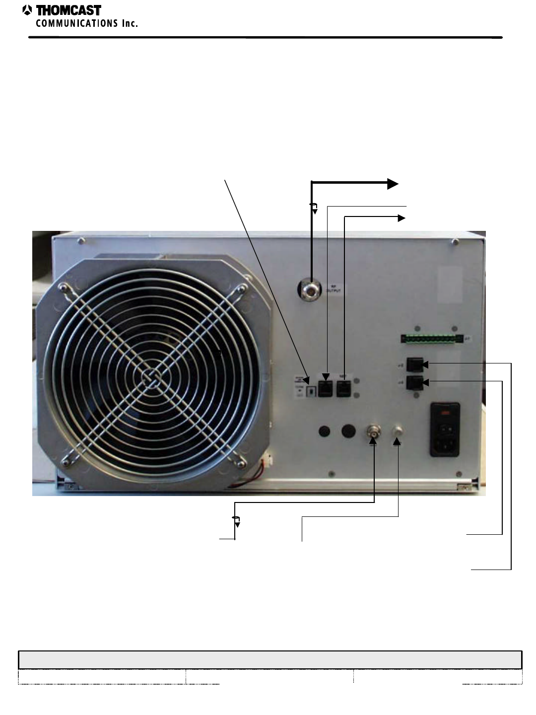
EXTERNAL INTERCONNECTIONS, SDxxxxC Series
COMWAVE DIVISION External Interconnections for the SDxxxxC Series
All information contained in this document is confidential and proprietary to THOMCAST and shall not be disclosed without the prior written permission of THOMCAST.
CREATED: KAS 2/10/00 CHECKED: DMW 2/14/00 RELEASED: PRC 2/14/00
Document #: DOC30-0043 REV: FEB.10.00 1
SUB-CHASSIS REAR PANEL
IF Input Signal
RF Output
Super-flex cable
In from ComViewa
Out to ComViewa
Termination Switch
OPTIONAL Agile
Controller
Local RS-485
communication
Freq Ref In
NOTES: a) These are interchangeable.
COMWAVE DIVISION
All information contained in this document is confidential and proprietary to THOMCAST and shall not be disclosed without the prior written permission of THOMCAST.
CREATED: KAS 1/18/99 CHECKED: DMW 1/18/99 RELEASED: PRC 1/18/99
Document #: DOC30-0005 REV: NOV.11.99 ECO #: 98-116 1
COMVIEW STATUS MONITORING INTERCONNECTIONS
COMWAVE
STATUS
MONITORING
SYSTEM
NOTE: Position
switch to TERM for last
drawer in the series
LAST DRAWER IN
SERIES
TO FINAL
DRAWER IN THE
SERIES
TERM
OUT
NETWORK END
TERMINATION NET NET
TERM
OUT
NETWORK END
TERMINATION NET NET
TERM
OUT
NETWORK END
TERMINATION NET NET
TERM
OUT
NETWORK END
TERMINATION NET NET
ComView Status Monitoring Interconnections

1
Turn-On Procedure for the SDxxxxC Series of Transmitters
COMWAVE DIVISION
All information contained in this document is confidential and proprietary to THOMCAST and shall not be disclosed without the prior written permission of THOMCAST.
CREATED: KAS ................................................................2/10/00 CHECKED: PRC...............................................................2/10/00 RELEASED: DMW............................................................ 2/14/00
Document #: DOC26-0050
REV: FEB.10.00
TURN-ON PROCEDURE
INITIAL TURN-ON PROCEDURE
1. Plug the AC line in.
2. Ensure all external interconnections are appropriately connected.
3. Turn the power switch on the rear of the transmitter to the “ON” position.
4. All modules perform an automatic start up program.
♦ Upconverter Plug-in Module
A lamp test operation is performed. All chassis front panel LED’s are illuminated for approximately 1
second then darkened. The lamp test allows a quick verification that all front panel LED’s are functioning.
In addition, the lamp test is a clear outward sign that the MCU board is receiving power, is executing the
firmware program, and has recovered from RESET. Shortly after the lamp test, the LED’s will display
chassis status as determined by firmware tests. Document # DOC13-0188 discusses the firmware in more
detail.
♦ LO Plug-in Module
When the LO module is turned on, the code executes an initialization process. This process provides a
lamp test, and displays the channel number on the front panel eight-segment LED display. An internal
reference is adjusted to operational frequency, and the synthesizer chip is programmed with the
operational frequency that was previously set into the microprocessor’s non-volatile memory.
Additionally, the working arrays and structures of the application are set into RAM. After the initialization
program completes, the code enters a simple state machine to judge and operate the LO module.
Document # DOC13-0184 discusses the firmware in more detail.
♦ Power Supply Plug-in Module
When power is initially supplied to the power supply module a lamp test is performed. The two front
panel LED’s will flash on then off, after which the LED’s remain lit, verifying operation.
5. Once the start up program is complete the equipment is functional.
NORMAL OPERATION
The following LED’s confirm normal operation:
LO plug-in module
ë DC POWER – continuously illuminated green
ë LO Ø LOCK - unlit
Power supply plug-in module
ë POWER - continuously illuminated green
ë DC POWER - continuously illuminated green
Refer to the troubleshooting section of this manual for more information about the above LED’s.

2
Turn-On Procedure for the SDxxxxC Series of Transmitters
COMWAVE DIVISION
All information contained in this document is confidential and proprietary to THOMCAST and shall not be disclosed without the prior written permission of THOMCAST.
CREATED: KAS ................................................................2/10/00 CHECKED: PRC...............................................................2/10/00 RELEASED: DMW............................................................ 2/14/00
Document #: DOC26-0050
REV: FEB.10.00
Power Amplifier Segment
Operation is accomplished by turning the key-lock switch to the “ON/LOCKED” position.
• The locks are an added safety feature; however, the keys are interchangeable.
The POWER/FAULT LED should continuously illuminate GREEN. If the LED flashes RED, the power amplifier
segment has faulted. After three faults, a failure will occur and the segment will shut down. Turning the key-lock
switch to the “OFF/UNLOCKED” position and then back to the “ON/LOCKED” position will reset it. Should failure
occur again, hot replacement is necessary. Turn the key-lock switch to the “OFF/UNLOCKED” position and pull the
failed segment out of the rack by the handle. Slide a new power amplifier segment into the vacant space, see the
installation procedure for assistance, set the correct node address, see DOC22-0019, and turn the key-lock switch to the
“ON/LOCKED” position.
SECTION 3
PREVIOUS
Print

1
Recommended Test Equipment
COMWAVE DIVISION
All information contained in this document is confidential and proprietary to THOMCAST and shall not be disclosed without the prior written permission of THOMCAST.
CREATED: KAS ................................................................11/18/99 CHECKED: DP .................................................................2/7/00
RELEASED: PC
................................................................ 3/5/00
Document #: DOC25-0007
REV: APR.05.00
RECOMMENDED TEST EQUIPMENT
The following test equipment can be substituted with other models in most cases; Comwave suggests that you use
equipment that will produce equivalent or better results. An asterisk (*) represents the minimum equipment
necessary; these items are required during the initial MMDS system set up and should be available at all times.
The remaining test equipment is useful for a variety of test and performance checks including verification of
compliance with FCC rules and troubleshooting suspected problem areas or failures when used by qualified
personnel.
Due to the many variables in maintenance and system requirements of television transmission systems, this list
should only be used as a guide in your test equipment selection.
Table 1: Suggested test equipment.
MODEL EQUIPMENT TYPICAL USES
Tektronix
TSG-100 *Video generator
Can be substituted for the normal program video to help determine a
problem with the incoming video from either the satellite receiver or
from off-air demodulation. Useful when comparing channels or when
an unchanging video signal is required. May also be used to set
modulation levels for the transmitter and the encoding system.
Fluke 87 *Digital voltmeter, 3 ½ digit
HP 435B 10 MHz to 3 GHz power
meter
Used in conjunction with various attenuators to measure power at
various points throughout the transmitter when troubleshooting
problems. Also verifies an MMDS transmitter is operating at the
proper output power.
HP 8482H Sensor for power meter
Used in conjunction with various attenuators to measure power at
various points throughout the transmitter when troubleshooting
problems. Also verifies an MMDS transmitter is operating at the
proper output power.
HP 8594A
Option 010
Option 301
Spectrum analyzer (with
options)
Tracking generator
TV Sync trigger
Useful in measuring power, troubleshooting problems, comparing
levels and setting modulation depths. In conjunction with a separate or
built in sweep generator, it can measure VSWR of
antenna/transmission line system. The ultimate piece of test equipment.
*13” or larger color TV
monitor/receiver
A cable ready TV receiver is required to insure that a good quality
picture is being transmitted. A video monitor is essential in observing
the quality of the signal received by either the satellite receivers or off-
air demodulators prior to processing, scrambling, and converting to an
MMDS channel for transmitting.
*Oscilloscope, 10 MHz
Required along with a 75 Ω termination to properly set up the 1 volt
P/P video required by the MMDS transmitter. Also a mandatory item
when setting the encoder system. Very useful when troubleshooting
system problems.
*MMDS block down
converter Converts a sample of the MMDS signal that is being transmitted to a
VHF signal required by the TV receiver of decoder.
PREVIOUS
Print

2
Recommended Test Equipment
COMWAVE DIVISION
All information contained in this document is confidential and proprietary to THOMCAST and shall not be disclosed without the prior written permission of THOMCAST.
CREATED: KAS ................................................................11/18/99 CHECKED: DP .................................................................2/7/00
RELEASED: PC
................................................................ 3/5/00
Document #: DOC25-0007
REV: APR.05.00
MODEL EQUIPMENT TYPICAL USES
*Decoder (type and model
determined by type of
encoding or scrambling
system used)
Required between the block down converter and TV receiver to
unscramble a scrambled signal.
Narda 3003-20 *20 dB “S” band directional
coupler Provides a reduced sample of the transmitted MMDS signal to various
test instruments.
Narda 771-20 *20 dB microwave attenuator Provides a reduced sample of the transmitted MMDS signal to various
test instruments.
Narda 771-60 *60 dB microwave attenuator Provides a reduced sample of the transmitted MMDS signal to various
test instruments.
Narda 771-10 *10 dB microwave attenuator Provides a reduced sample of the transmitted MMDS signal to various
test instruments.
*75 Ω terminations
*50 and 75 Ω cables
*Assorted BNC, N, RCA,
and F type adapters
1
Troubleshooting for the SDxxxxC Series of Transmitters
COMWAVE DIVISION
All information contained in this document is confidential and proprietary to THOMCAST and shall not be disclosed without the prior written permission of THOMCAST.
CREATED: KAS ................................................................2/10/00 CHECKED: AAC .............................................................. 2/15/00RELEASED: PRC .............................................................. 2/16/00
Document #: DOC18-0073
REV: FEB.16.00
SDxxxxC SERIES TROUBLESHOOTING
This series of transmitters is equipped with comprehensive diagnostic circuitry that monitors the status of each plug
in module and power amplifier segments so failures can be readily detected. Observing the front panel LED
diagnostic display, and ComView interface will inform you of the complete operational status. The following lists
explain various failure mode displays and possible solutions.
A 14-pin computer type diagnostic interface connector, labeled J1, is located on the rear of the transmitter to assist
in troubleshooting. Critical power supply, module, and motherboard voltage test points can be accessed/monitored
at this location. Should a failure occur, the combination of diagnostic LED status lights, diagnostic interface voltage
test points, and ComView should help identify the failure.
• Repair of internal modules is not recommended or advised. Contact1 COMWAVE customer support should a
failure occur.
LO PLUG-IN MODULE:
The LED’s listed below continuously illuminate GREEN during normal operation. Absence of a green LED
indicates a missing signal or parameter that results in a controlled automatic shutdown
DC POWER
(No power present)
CAUSES: CHECK FOR: REMEDY:
Plug-in module not seated
properly If LO plug-in module LED’s are unlit,
while the power supply plug-in LED’s
are lit
Remove LO plug-in and push firmly back
in place
Power supply plug-in
module malfunctioning If LO AND power supply plug-in
LED’s are unlit Remove the panel covering the front end
power supply and check the LED’s
Front end power supply
malfunctioning If the LED’s indicate a problem, refer
to Table 1
If no problem is indicated
If the fuse is bad
If the fuse is ok
Contact1 Comwave customer support for
a replacement
Check the rear panel AC fuse
Replace it
Contact1 Comwave customer support
Table 1: Front end power supply alarm indicators & control signals.
Description Signal LED Indicator
Output OK Yes Green
Supply Standby Yes Amber
Supply Fail Yes Red
Current Limit Yes Amber
Overvoltage Yes Red
Overtemp Yes Amber (same as Fan Fail LED indicator)
AC Undervoltage Yes NA
Fan Fail Yes Amber (same as Overtemp LED indicator)
1 DOC20-0001 provides detailed contact information. International phone 001-570-474-6751, USA & Canada phone 1-800-266-9283.
2
Troubleshooting for the SDxxxxC Series of Transmitters
COMWAVE DIVISION
All information contained in this document is confidential and proprietary to THOMCAST and shall not be disclosed without the prior written permission of THOMCAST.
CREATED: KAS ................................................................2/10/00 CHECKED: AAC .............................................................. 2/15/00RELEASED: PRC .............................................................. 2/16/00
Document #: DOC18-0073
REV: FEB.16.00
The following LED’s remain unlit until a malfunction is detected then they continuously illuminate RED. Loss of
phase lock results in controlled automatic transmitter shut down.
LO Ø LOCK
(Loss of phase lock)
CAUSES: REMEDY:
Reference Level Measure the reference level at the rear of the
transmitter
If the level is low:
Check and tighten all external cables and
harnesses associated with the LO
If the level is OK or still low after checking the
cables:
Contact2 Comwave customer support for a
replacement
POWER SUPPLY PLUG-IN MODULE:
The LED’s listed below continuously operate GREEN during normal operation. Absence of a green LED indicates
a missing signal or parameter that results in a controlled automatic shutdown
POWER
(No power present from the front end power supply)
CAUSES: REMEDY:
Blown fuse, F1, in plug-in module Replace fuse
No DC input from front end power supple Check OEM power supply
Failure in plug-in module Contact2 Comwave customer support for a replacement
DC POWER
(No output power)
CAUSES: REMEDY:
Short circuit or current overload Test 48 pin connector on back plane for short circuits
Find plug-in module that is causing overload by
swapping with like plug-in modules
Failure in plug-in module Contact2 Comwave customer support for a replacement
The upconverter / amplifier plug-in module LCD display provides operating information about each plug-in module,
i.e. ‘PASS’ / ‘FAIL’, as well as a series of measurements, and user adjustments.
To view the status of each plug-in module perform the following steps:
1. Use the keypad on the upconverter / amplifier plug-in, choose select, when Status is displayed in LCD
hit enter.
2. At this point you will be able to “select” the plug-in module of your choice.
3. When you’ve chosen the appropriate module the LCD will display either ‘PASS’ or ‘FAIL’.
4. If it indicates the plug-in has failed, contact2 Comwave for a replacement plug-in, there are no user
troubleshooting steps for the plug-in modules.
2 DOC20-0001 provides detailed contact information. International phone 001-570-474-6751, USA & Canada phone 1-800-266-9283.

3
Troubleshooting for the SDxxxxC Series of Transmitters
COMWAVE DIVISION
All information contained in this document is confidential and proprietary to THOMCAST and shall not be disclosed without the prior written permission of THOMCAST.
CREATED: KAS ................................................................2/10/00 CHECKED: AAC .............................................................. 2/15/00RELEASED: PRC .............................................................. 2/16/00
Document #: DOC18-0073
REV: FEB.16.00
If the Reflected Power measurement is high, check the following:
1. Output cable
2. Output Notch Filter (present at the output of the system)
3. Cable between Notch Filter and Channel Combiner (if present at the output of the system)
4. Connections to the antenna
If after ensuring the above are properly connected the problem persists, contact3 Comwave customer support.
If the Forward Power measurement is low, check the following:
1. Check the power amplifier segment LED’s; they should be green.
2. Check the status of each of the plug-in module via the keypad on the upconverter / amplifier plug-in front panel,
see above for steps. They should all present a PASS condition.
3. If no amplifier segment or plug-in modules indicate a FAIL condition, use the keypad and LCD to display the
IN-SIGNAL condition.
4. If the IN-SIGNAL status indicates a NO IN-SIGNAL condition, check the signal source.
5. If any power amplifiers segments and / or plug-ins have a FAIL condition, contact Comwave customer support
to report the failure and receive a replacement.
POWER AMPLIFIER SEGMENT
Hot replacement of the power amplifier segment may be required if a failure occurs. To remove a segment, turn the
key-lock switch to the OFF position, loosen the thumbscrews on the segment’s front panel and slide the failed
segment out of the sub-rack. Before the replacement segment can be installed, the node address must be set, refer to
document # DOC22-0019. A set of DIP switches is accessible through the cover of each segment directly behind
the key-lock switch. Set the DIP switches of the replacement segment to the same positions as the failed segment’s
DIP switches. Refer to the installation procedure for assistance when replacing power amplifier segments.
3 DOC20-0001 provides detailed contact information. International phone 001-570-474-6751, USA & Canada phone 1-800-266-9283.
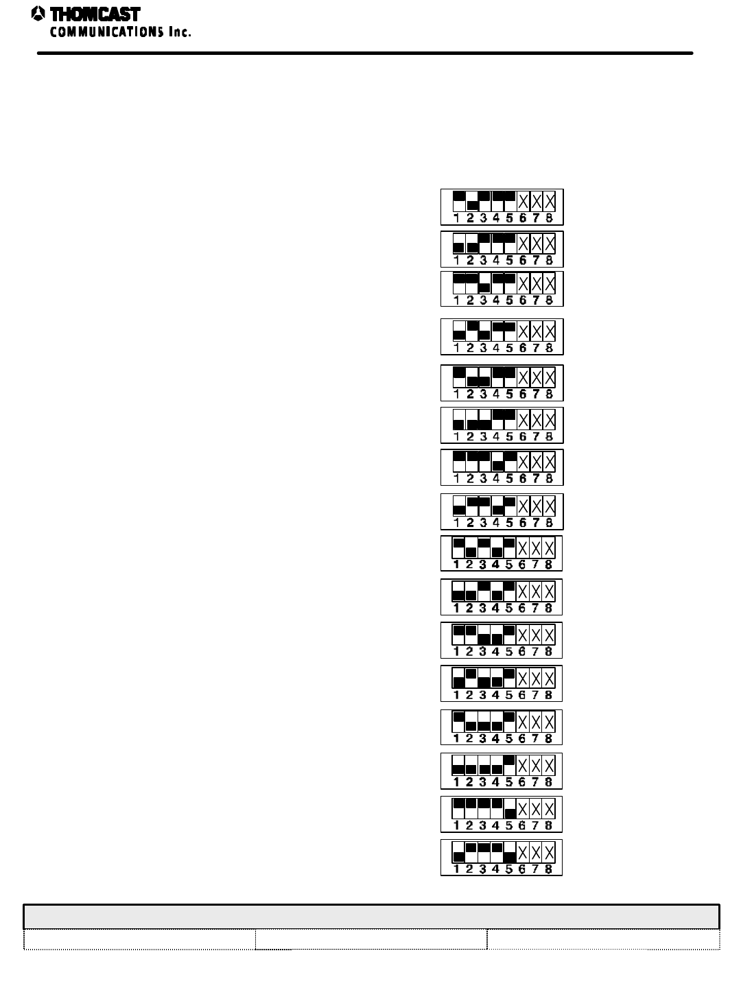
COMWAVE DIVISION Power Amplifier Segment Node Addresses
All information contained in this document is confidential and proprietary to THOMCAST and shall not be disclosed without the prior written permission of THOMCAST.
CREATED: KAS 9/16/98 CHECKED: DMW 10/20/98 RELEASED: PRC 10/20/98
Document #: DOC22-0019 REV: DEC.01.99 ECO #: 98-116 1
NODE ADDRESSES
1 to 16 Channels
NOTE: Do not change
node switch Settings 6, 7,
and 8. They should
remain as set by the
factory.
MODULE POSITION NODE ADDRESS NODE SWITCH SETTING
1ON
OFF
ON
OFF
ON
OFF
ON
OFF
ON
OFF
ON
OFF
ON
OFF
ON
OFF
ON
OFF
ON
OFF
ON
OFF
ON
OFF
ON
OFF
ON
OFF
ON
OFF
ON
OFF
2
2
3
4
4
3
6
5
5 6
7
8
9
7
8
9 10
14
15
16
17
12
13
1110
13
14
15
16
11
12
1
SDxxxC Series Transmitter Troubleshooting Worksheet
– 47266066 Rear Panel Interface
COMWAVE DIVISION
All information contained in this document is confidential and proprietary to THOMCAST and shall not be disclosed without the prior written permission of THOMCAST.
CREATED: AB ..................................................................2/4/00 CHECKED: KAS ...............................................................2/9/00
RELEASED: PRC
............................................................. 2/11/00
Document #: DOC18-0072
REV: FEB.09.00
TROUBLESHOOTING WORKSHEET
This troubleshooting worksheet identifies each interface pin, the associated internal test point, nominal value, and
the expected voltage range. Please fill in all blank spaces completely
J1: Rear Panel
Diagnostic Pin Function Checked Measured Voltage
1Ground
2LO / Front-End Fault
3PS Fault
4Upconv Fault
5Sys Pwr
6REFL Pwr
7+48V Fault Input
8+10V Fault Input
9P.A.S. Reset
10 P.A.S. Standby
11 Amp Seg Fault
12 +12V Output
13 Insignal for Booster
14 Ground
FILL IN ALL THE ABOVE BLANK SPACES COMPLETELY
COMPANY NAME: ________________________ CUSTOMER’S NAME: ________________________
PHONE NUMBER: ________________________ FAX NUMBER: ________________________
MODEL: __________ CHANNEL: ____________ SERIAL NUMBER (REAR PANEL): _____________
SEND RESULTS TO: THOMCAST COMMUNICATIONS, COMWAVE DIVISION
ATTENTION TECHNICAL SUPPORT
TOLL FREE PHONE (U.S.A. & Canada): 1-800-COMWAVE (1-800-266-9283)
International and U.S.A. 1-570-474-67511
FAX 1-570-474-5469
1 International calls must dial the country code before the phone number, i.e. 001-570-474-6751.
1
SDxxxxC Series Transmitter Fusing & Protection
COMWAVE DIVISION
All information contained in this document is confidential and proprietary to THOMCAST and shall not be disclosed without the prior written permission of THOMCAST.
CREATED: KAS ................................................................2/10/00 CHECKED: DMW.............................................................2/14/00
RELEASED: PRC
............................................................. 2/16/00
Document #: DOC18-0075
REV: FEB.16.00
SDxxxxC SERIES TRANSMITTER FUSING AND PROTECTION
Resettable and replaceable fuses1 are found in this system. Refer to the tables below for fuse locations and values.
Table 1: Transmitter fuse locations.
LOCATION REFERENCE VALUE
Rear Panel Interface Board - 47266066 F1 .5 ampere resettable
Rear Panel AC Input 8 amperes @ 230 VAC
Table 2: Power amplifier segment fuse locations.
LOCATION REFERENCE VALUE
Microcontroller board F1, F2 .75 amperes resettable
Microcontroller board F3 .30 amperes resettable
Microcontroller board F4 .35 amperes resettable
DC - DC converter board F1 10 amperes
Thermal Protection: Thermal protection is accomplished using temperature sensors within individual plug-in
modules. The LO module does not have a temperature sensor. When the temperature exceeds 140° Fahrenheit (60°
Celsius), the sensors inform the microcontroller which then takes the appropriate action, until the unit is sufficiently
cooled.
Interlocks: Interlocks are performed via software applications, see individual plug-in modules firmware description
for more information.
The OEM front end power supply offers the following:
Table 3: Front end power supply alarm indicators & control signals.
Description Signal LED Indicator
Output OK Yes Green
Supply Standby Yes Amber
Supply Fail Yes Red
Current Limit Yes Amber
Overvoltage Yes Red
Overtemp Yes Amber (same as Fan Fail LED indicator)
AC Undervoltage Yes NA
Fan Fail Yes Amber (same as Overtemp LED indicator)
1 Replace only with the same type and rating.

1
Power Supply Plug-In - Fusing and Protection
COMWAVE DIVISION
All information contained in this document is confidential and proprietary to THOMCAST and shall not be disclosed without the prior written permission of THOMCAST.
CREATED: CTS ................................................................1/26/00 CHECKED: KAS ...............................................................1/27/00
RELEASED: CTS
.............................................................. 2/14/00
Document #: DOC18-0071
REV: JAN.27.00
POWER SUPPLY PLUG-IN FUSING AND PROTECTION
This module contains one replaceable fuse1, refer to the table below for fuse location and value.
Table 1: Transmitter fuse locations.
LOCATION REFERENCE VALUE
DC converter board F1 6 amperes @ 117/230 VAC
CURRENT AND VOLTAGE MONITORING
Current sampling is accomplished by measuring the voltage drop across a resistor in series of the load. The voltages
from both sides of the resistor are scaled down in order to keep the measured voltages from the supply voltages of
the operational amplifiers. The voltage differences are first buffered, and then applied to an operational amplifier
configured to measure the difference of the two input voltages.
The output of the differential amplifier is then applied to a non-inverting amplifier to increase the voltage near the
middle of the system controller’s 5 volt analog to digital converter’s range. An integrated circuit containing Zener
and Shottkey diodes protect the inputs of the system controller. The system controller compares this value against
previously calibrated values to determine if the power supply is operating outside of specified parameters.
The input buffers for the current sampling also provide the voltage samples; the buffer’s output is scaled down by
dividing resistors. This provides a sample voltage to the analog to digital converters that is mid-rage between zero
and five volts.
All of the power supply sections operate in a similar manner. The –12 VDC power supply section uses inverting
amplifiers (instead of buffers) with unity gain to convert the sample values to positive representations of the sampled
voltages.
The current and voltage sample outputs are applied to an analog multiplexer integrated circuit. This chip selects the
group of signals that are applied to the microprocessor from a control provided from the microprocessor.
TEMPERATURE SENSING
Temperature sensing is accomplished by a thermal sensing integrated circuit. This integrated circuit outputs an
analog voltage between 0 and 5 volts that corresponds to the relative air temperature.
This analog signal is applied to the analog to digital converter built into the embedded controller. The controller
processes this value and compares it against pre-determined values to control the sequence of events needed when
an over temperature condition arises
1 Replace only with the same type and rating.
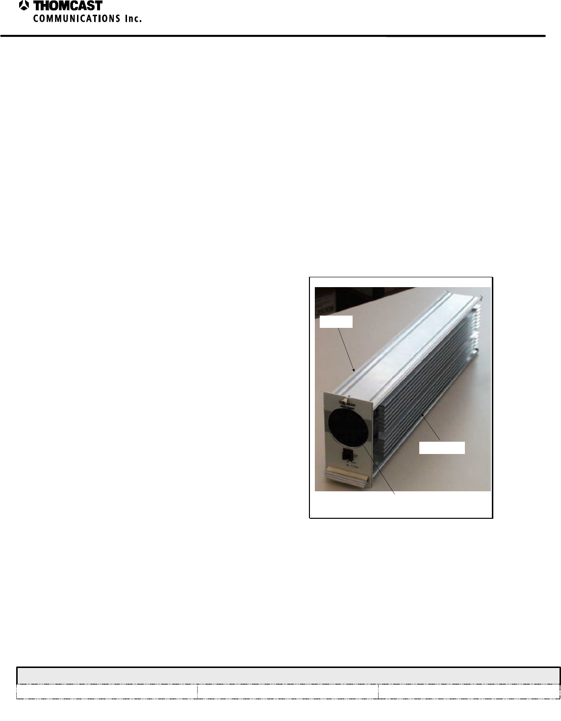
1
Maintenance for the
SDxxxxC Series of Transmitters
COMWAVE DIVISION
All information contained in this document is confidential and proprietary to THOMCAST and shall not be disclosed without the prior written permission of THOMCAST.
CREATED: KAS ................................................................2/10/00 CHECKED: DMW ............................................................. 2/11/00 RELEASED: PRC .............................................................. 2/11/00
Document #: DOC18-0074
REV: FEB.10.00
MAINTENANCE
COMWAVE products have been carefully designed to be maintenance free. Only periodic inspection and cleaning
is necessary.
INSPECTIONS
1. Periodically inspect cooling fans on the rear door of the rack and the heatsinks of the power amplifier segments
for heavy accumulations of dirt and/or insects. Heavy accumulation of foreign debris impedes cooling
effectiveness and could lead to premature failure. Should any debris be detected, shut down the transmitter and
follow the cleaning instructions to remove debris from transmitter.
• The agile transmitter will automatically recover the channel of the transmitter that is being cleaned.
2. After performing routine maintenance, be sure to check the tightness of all cable connections and especially the
integrity of crimp type connectors.
CLEANING
POWER SUPPLY PLUG-IN MODULE:
1. Pull the plug-in out of the sub-chassis and vacuum
the heatsink.
2. Remove the side “snap-on” cover and clean the
front panel fan.
3. Replace the cover.
4. Plug the segment back in.
• Be sure not to bend or damage the fins of the
heatsink during cleaning.
• Keep in mind that when the plug-in module is
removed there will be an interruption in service,
which will be restored immediately upon its return to
the sub-chassis.
HEATSINK
COVER
FAN
Figure 1: Power supply plug-in module.
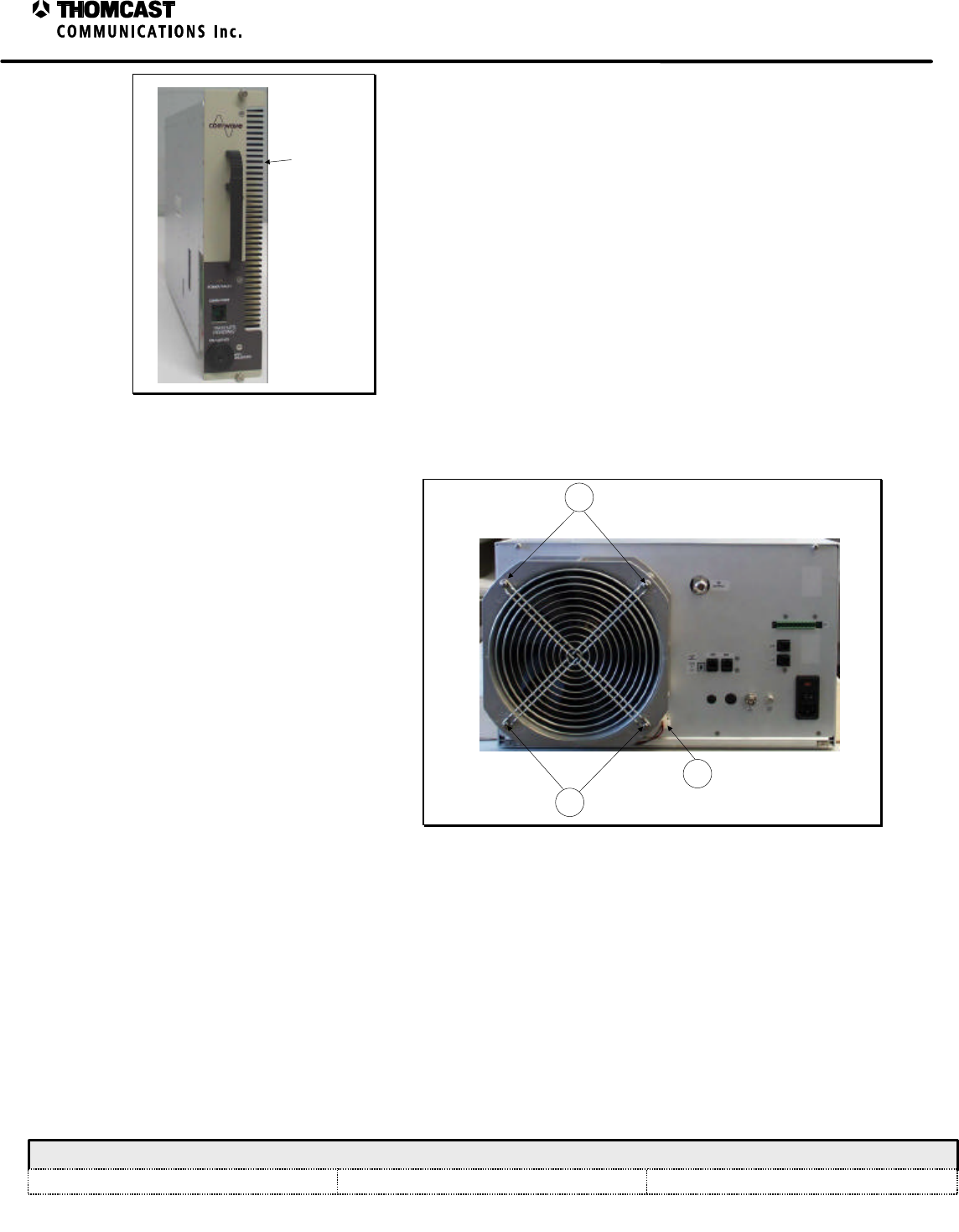
2
Maintenance for the
SDxxxxC Series of Transmitters
COMWAVE DIVISION
All information contained in this document is confidential and proprietary to THOMCAST and shall not be disclosed without the prior written permission of THOMCAST.
CREATED: KAS ................................................................2/10/00 CHECKED: DMW ............................................................. 2/11/00 RELEASED: PRC .............................................................. 2/11/00
Document #: DOC18-0074
REV: FEB.10.00
HEATSINK
Figure 2: Power amplifier segment heatsink.
POWER AMPLIFIER SEGMENTS:
Pull each power amplifier segment one at a time from the front
of the rack and vacuum the heatsinks. Due to the hot
replacement feature, if one segment is removed at a time, the
transmitter does not need to be turned off. Plug the segment
back in after cleaning.
• Be sure not to bend or damage the fins of the heatsinks
during cleaning.
FAN:
Clean the fan on the rear of the sub-chassis,
removing the fan guard if necessary.
1. Power connection; remove the power
prior to cleaning.
2. To remove the fan guard remove these
screws. 1
2
2
Figure 3: Rear panel fan.

1
Calibrations for the SDxxxxC Transmitter Series
COMWAVE DIVISION
All information contained in this document is confidential and proprietary to THOMCAST and shall not be disclosed without the prior written permission of THOMCAST.
CREATED: AAC................................................................2/14/00 CHECKED: KAS ...............................................................2/14/00
RELEASED: PRC
............................................................. 2/16/00
Document #: DOC16-0057
REV: FEB.16.00
CALIBRATIONS FOR THE SDxxxxC TRANSMITTER SERIES
This series of transmitters is designed to perform auto-calibration upon turn-on. Once this is complete if the output
power is incorrect or missing proceed as follows.
FORWARD POWER – UPCONVERTER / AMPLIFIER PLUG-IN MODULE:
1) Make connections as depicted in Figure 1 note 1.
2) Connect a PC with the application file DRIVER_PLUG_IN_CAL_&_ADJUS to the RS-232 port on the front
panel.
3) Initialize DRIVER_PLUG_IN_CAL_&_ADJUS application.
4) Through the program application, specifically in the POWER CONTROL BOX, set the POWER MODE to
MANUAL.
5) With the MANUAL POWER CONTROL sliding button, set power in order to have a reading of 20 dBm
(100mW) at the external power meter. Account for the directional coupler factor.
6) Enter the number 20 in the DRIVER FORWARD POWER SET VALUE field.
7) Press the DRIVER FORWARD POWER CALIBRATE button.
8) On the upconverter plug-in, display the Forward Power measurement by:
a) (Considering the LCD display is in its default state): SELECT (to make the STATUS option of the
STATUS / CALIBRATE screen to flash)
b) ENTER (to display PS / LO / DRIVER status screen)
c) SELECT, SELECT (to highlight the DRIVER STATUS option)
d) ENTER (to display options INSIGNAL / SYSTEM FORWARD POWER / SYSTEM REFLECTED
POWER / DRIVER FORWARD POWER under the DRIVER STATUS menu)
e) SELECT, SELECT and SELECT (to highlight the DRIVER FORWARD POWER)
f) Enter to display the measurement
9) Verify that the reading on the LCD display is consistent with the reading on the external power meter. Output
power of the upconverter plug-in is now calibrated.
10) Close DRIVER_PLUG_IN_CAL_&_ADJUS application and disconnect PC.
11) Return the system to its original interconnections.
2
Calibrations for the SDxxxxC Transmitter Series
COMWAVE DIVISION
All information contained in this document is confidential and proprietary to THOMCAST and shall not be disclosed without the prior written permission of THOMCAST.
CREATED: AAC................................................................2/14/00 CHECKED: KAS ...............................................................2/14/00
RELEASED: PRC
............................................................. 2/16/00
Document #: DOC16-0057
REV: FEB.16.00
Open sub-chassis rear panel
FWD
REFL
* This item should be an N-N male extension PN UG-57B/U or equiv. Substitution of this adapter requires that its insertion loss be known for accurate power measurements.
- 30 dB
Directional
Coupler
TO SPECTRUM
ANALYZER OR TO POWER
METER
50 OHM
TERMINATION
Upconverter / Amplifier Plug-in Front panel
cable
1
- 30 dB
Directional
Coupler
TO SPECTRUM
ANALYZER OR TO POWER
METER
50 OHM
TERMINATION
2
NOTES:
1) Connection for upconverter plug-in
calibration.
2) Connection for system calibration.
Figure 1: Calibration interconnections.
FORWARD POWER – SYSTEM:
1) Make connections as depicted in Figure 1 note 2.
2) Connect a PC with the application file DRIVER_PLUG_IN_CAL_&_ADJUS to the RS-232 port on the front
panel.
3) Initialize DRIVER_PLUG_IN_CAL_&_ADJUS application.
4) Through the program application, specifically in the POWER CONTROL BOX, set the POWER MODE to
MANUAL.
5) With the MANUAL POWER CONTROL sliding button set power in order to have a reading of 44 dBm (25W)
for the SD2500C and 47 dBm (50W) for the SD5000C at the external power meter. Account for the directional
coupler factor.
6) Enter the same number as above in the SYSTEM FORWARD POWER SET VALUE field.
7) Press the SYSTEM FORWARD POWER CALIBRATE button.
8) On the upconverter plug-in, display the Forward Power measurement by:
a) (Considering the LCD display is in its default state): SELECT (to make the STATUS option of the
STATUS / CALIBRATE screen to flash)
b) ENTER (to display PS / LO / DRIVER status screen)
c) SELECT, SELECT (to highlight the DRIVER STATUS option)

3
Calibrations for the SDxxxxC Transmitter Series
COMWAVE DIVISION
All information contained in this document is confidential and proprietary to THOMCAST and shall not be disclosed without the prior written permission of THOMCAST.
CREATED: AAC................................................................2/14/00 CHECKED: KAS ...............................................................2/14/00
RELEASED: PRC
............................................................. 2/16/00
Document #: DOC16-0057
REV: FEB.16.00
d) ENTER (to display options INSIGNAL / SYSTEM FORWARD POWER / SYSTEM REFLECTED
POWER / DRIVER FORWARD POWER under the DRIVER STATUS menu)
e) SELECT, SELECT and SELECT (to highlight the DRIVER FORWARD POWER)
f) Enter to display the measurement
9) Verify that the reading on the LCD display is consistent with the reading on the external power meter. Output
power of the System is now calibrated.
10) Set POWER MODE to AUTO
11) Slide AUTO POWER CONTROL to recover power to the value previously read at the external power meter (if
necessary).
12) Re-check the upconverter plug-in LCD reading.
13) Close DRIVER_PLUG_IN_CAL_&_ADJUS application and disconnect PC.
14) Return the system to its original interconnections.
SYSTEM REFLECTED POWER CALIBRATION:
1) If you haven’t already performed the system forward power calibrations do so now, as described above,
omitting steps 13 and 14.
2) Put the system in stand-by with the program application.
3) On the upconverter plug-in, display the Forward Power measurement by:
a) (Considering the LCD display is in its default state): SELECT (to make the STATUS option of the
STATUS / CALIBRATE screen to flash)
b) ENTER (to display PS / LO / DRIVER status screen)
c) SELECT, SELECT (to highlight the DRIVER STATUS option)
d) ENTER (to display options INSIGNAL / SYSTEM FORWARD POWER / SYSTEM REFLECTED
POWER / DRIVER FORWARD POWER under the DRIVER STATUS menu)
e) SELECT, SELECT and SELECT (to highlight the DRIVER FORWARD POWER)
f) Enter to display the measurement
4) Swap FORWARD and REFLECTED POWER cables coming out of the output coupler.
5) Enter the number 44 for an SD2500C system and 47 for an SD5000C system in the SYSTEM REFLECTED
POWER SET VALUE field.
6) Put the system in TRANSMIT MODE.
a) While performing steps 7 and 8 the system will shut down due to the high-reflected power simulated
measurement, this is necessary; if these steps are completed within 5 seconds this will not occur.
7) Press the SYSTEM REFLECTED POWER CALIBRATE button.
8) Verify that the reading on the LCD display is consistent with the reading on the external power meter.
Reflected power of the System is now calibrated.
9) Once the system shuts down because of the high reflected power simulated measurement. Put it in STAND-BY
mode.
10) Put the FORWARD and REFLECTED POWER cables back to their original positions.
11) Set the system mode to TRANSMIT
12) Close DRIVER_PLUG_IN_CAL_&_ADJUS application and disconnect PC.
13) Return the system to its original interconnections.
SECTION 4
PREVIOUS
Print

1
Sub-Chassis Theory of Operation - 47266170
COMWAVE DIVISION
All information contained in this document is confidential and proprietary to THOMCAST and shall not be disclosed without the prior written permission of THOMCAST.
CREATED: AB ..................................................................2/01/00 CHECKED: KAS ...............................................................2/02/00
RELEASED: PRC
............................................................. 2/11/00
Document #: DOC14-0037
REV: FEB.02.00
SUB-CHASSIS THEORY OF OPERATION
The sub-chassis contains guide rails and houses the following components. Refer to Figure 1 for numerical
references.
1) One driver assembly, which is made up of three plug-in modules
a) LO plug-in
b) Power supply plug-in
c) Upconverter plug-in
The plug-in modules slide into the chassis on nylon card guides and connect to the driver back
plane board using a guide pin and a 48-position DIN connector.
The power supply plug-in module connects using a guide pin, 48-position DIN connector, and a 6-
position header. The header uses a DPDT push button switch to turn on the feed power only after
the plug-in module is fully inserted; this is to ensure that there is no arcing between connections
before the plug-in module is fully engaged. It also certifies that the module is properly grounded
before any voltage is applied.
2) A front-end DC power supply
This power supply is an OEM product and is hot swappable.
3) Up to four power amplifier segments
Each amplifier segment slides into the chassis on nylon slides and connects to the amplifier
motherboard via floating connectors10. The key-lock switch, located on the segments front panel,
must be in the OFF position in order to plug it in. This assures that all connections, mechanical
and electrical, are made before the amplifier is turned on.
Once the plug-in modules are in place, thumbscrews on the front panels are fastened to the sub-chassis to secure
them and provide a reliable ground connection. The key-lock switch on the amplifier segment is turned to the ON
position to apply power to the segment.
Floating OSP connectors9,10 mounted on the back plane board, the back panel of the chassis, the back of the plug-in
modules, and the back of the power amplifier segments, provide the interface for RF input and output. See
respective plug-in module theory of operation documentation for the location of the connectors.
4) Three communications boards
a) 47266064 - driver back plane board
See DOC13-0176 for more information about this board
b) 47266145 - amplifier motherboard and back plane
See DOC13-0183 for more information about this board
c) 47266165 - power supply back plane
See DOC13-0186 for more information about this board
2
Sub-Chassis Theory of Operation - 47266170
COMWAVE DIVISION
All information contained in this document is confidential and proprietary to THOMCAST and shall not be disclosed without the prior written permission of THOMCAST.
CREATED: AB ..................................................................2/01/00 CHECKED: KAS ...............................................................2/02/00
RELEASED: PRC
............................................................. 2/11/00
Document #: DOC14-0037
REV: FEB.02.00
SD2500C system shown
47266170 Sub-Chassis
2
4a
3
1b
11c
1a
NOTE: Boards 4b & 4c are
not visible in these photos.
9
(up to 4)
9
(up to 4)
10
(up to 4)
Figure 1: 47266170 sub-chassis.
Refer to Figure 2 for numerical references.
5) RF Splitter
This component divides the microwave signal of the driver in, up to 4, outputs to the power
amplifier segments. It can be used as a divider by 2, 3, or 4, depending on the total output power
of the equipment.
6) Power Combiner
The power combiner merges the output signal from the power amplifier segments into one
microwave output.
7) Directional Coupler
This piece of the equipment is used to measure forward and reflected power.
8) Power Detector
The power detector transforms the forward and reflected power signals from the directional
coupler into DC voltage to be processed in the upconverter / amplifier module.
3
Sub-Chassis Theory of Operation - 47266170
COMWAVE DIVISION
All information contained in this document is confidential and proprietary to THOMCAST and shall not be disclosed without the prior written permission of THOMCAST.
CREATED: AB ..................................................................2/01/00 CHECKED: KAS ...............................................................2/02/00
RELEASED: PRC
............................................................. 2/11/00
Document #: DOC14-0037
REV: FEB.02.00
Open sub-chassis rear panel
5
6
7
Figure 2: Sub-chassis, inside rear.
FRONT AND REAR PANEL DESCRIPTION
Front panel
The sub-chassis has no front panel; see respective plug-in module theory of operation documentation for a
discussion of front panel features.
Rear panel
Refer to Figure 3 for numerical references.
1) FAN: A rear mounted 48VDC fan provides system cooling. AC fan is optional.
2) RF OUT: RF output connector (Female N type).
3) COMMUNICATION PORTS: RJ11 phone jack connectors and a termination switch from the RS-485 board used
for communication to ComView.
4) J1: Female 14 pin header for diagnostics monitoring.
5) J2: RJ11 phone jack connector for OPTIONAL Agile controller.
6) J3: RJ11 phone jack connector for Local RS-485 communication.
7) FUSE: Main line fuse - 8amperes (used for 220V system only).
8) POWER SWITCH: Turn system on and off.
9) AC INPUT: AC Line input power cord connector.
10) FREQ REF IN: 75ohm Female F connector, external 10 MHz reference signal input.
11) FCC ID LABEL: Federal Communications Commission identification label.
12) IF INPUT: 75ohm Female BNC connector, input signal from an external source.
13) Not applicable in this model.
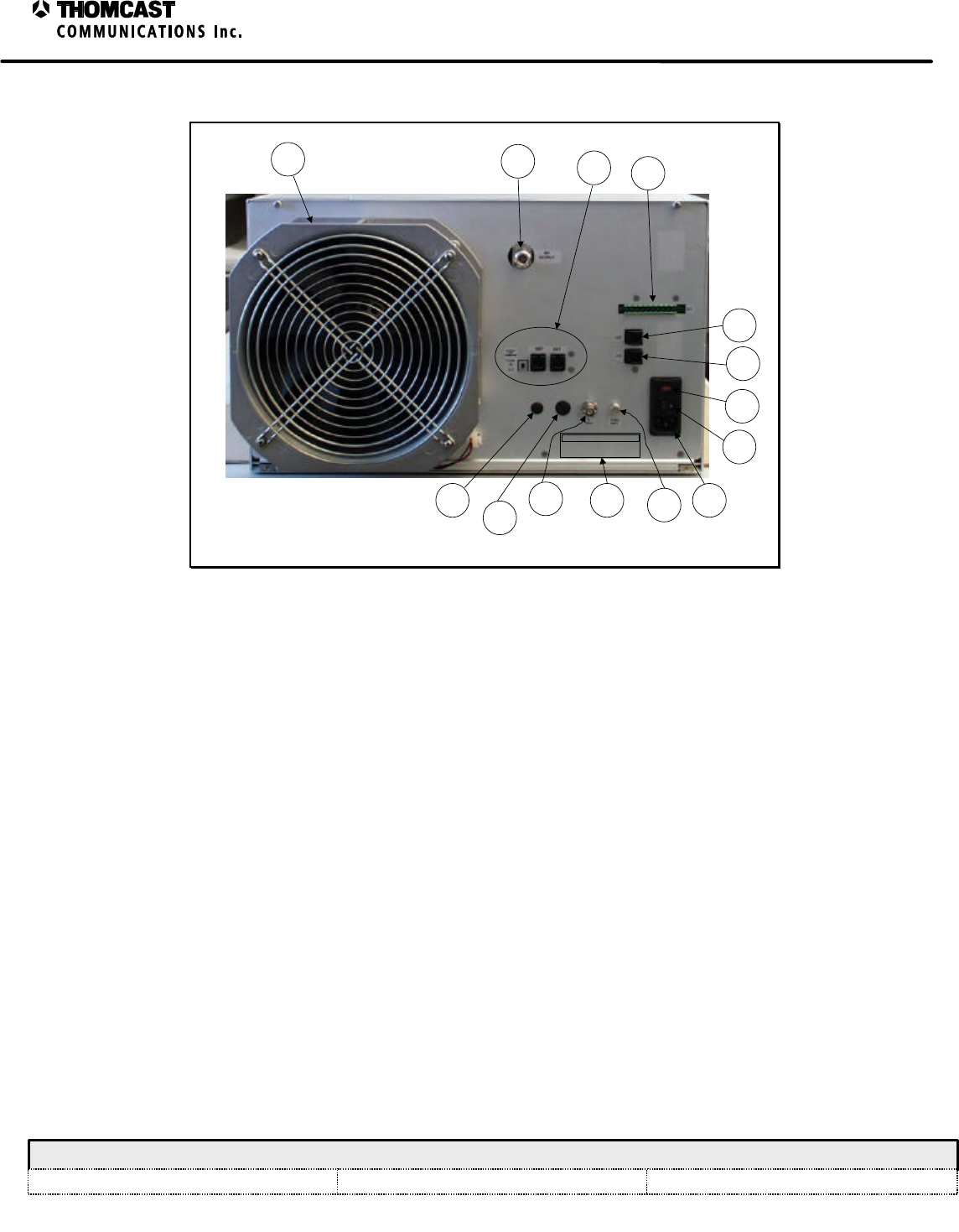
4
Sub-Chassis Theory of Operation - 47266170
COMWAVE DIVISION
All information contained in this document is confidential and proprietary to THOMCAST and shall not be disclosed without the prior written permission of THOMCAST.
CREATED: AB ..................................................................2/01/00 CHECKED: KAS ...............................................................2/02/00
RELEASED: PRC
............................................................. 2/11/00
Document #: DOC14-0037
REV: FEB.02.00
14) Not applicable in this model.
1234
5
6
7
8
9
10
FCC ID: CHP8BUSD5000C
MODEL SD5000C
5-50 WATTS AVG POWER TRANSMITTER
11
12
13
14
Figure 3: Sub-chassis rear panel.

1
Microcontroller Board (MCU) Description - 47266058
COMWAVE DIVISION
All information contained in this document is confidential and proprietary to THOMCAST and shall not be disclosed without the prior written permission of THOMCAST.
CREATED: CPU................................................................12/10/99 CHECKED: KAS ...............................................................1/27/00
RELEASED: PRC
............................................................. 2/10/00
Document #: DOC13-0175
REV: JAN.27.00
MICROCONTROLLER BOARD (MCU) DESCRIPTION
An MCU (microcontroller unit) circuit board assembly is contained within each plug-in module. The MCU
assembly hardware consists of a microcontroller IC and associated memory, a CPLD IC, and various analog and
logic support circuitry; the MCU operates under the control of a firmware program executed by the microcontroller.
Each plug-in module has it’s own firmware which is discussed in separate documents that can be found in the
respective modules section of the manual.
A variety of on-chip utilities and interfaces are integrated in the MCU, easing the support circuitry requirements and
simplifying the interfacing of the MCU to other circuit board resources. See Figure 1 for a block diagram of the
board.
The MCU is operated in an expanded mode, with program and data memory external to the MCU IC. The MCU
uses a 16 bit external data bus for interfacing to the memories. The firmware operating program is stored in IC U3,
a FLASH ROM memory. The storage is arranged and accessed in word (2 byte) mode. An address bus is provided
by the MCU to access the FLASH memory. The MCU and CPLD ICs provide additional control signals.
Two RAM ICs provide run-time data storage. U6 and U8 are 512 Kbyte static RAMs. The RAMs are served by the
MCU address bus and various support signals provided by the MCU and CPLD. Each RAM provides an 8 bit data
bus for reads and writes. By joining the two RAM data busses as low and high bytes on the 16 bit data bus, full 16
bit accesses are achieved.
Various glue logic, I/O, and register support functions are provided by IC U4, an in-circuit programmable CPLD.
The CPLD contains I/O registers that allow writes to and reads from MCU board signals such as AUX_OUT_A
through AUX_OUT_F, and ANALOG_ALARM_1 through ANALOG_ALARM_3. The CPLD registers are within
the MCU memory map and are accessed by the MCU through interfaces to the MCU address and data busses.
The CPLD register signals are used for accessing various on and off-board devices see Table 1.
Table 1: CPLD register signals.
Signal name Type (I/O) Application
Upconverter Local Oscillator System Controller
CS_A through CS_F ODAC address, AGC &
ALC module control SPI user enable N/A
AUX_OUT_A through
AUX_OUT_F OPS and ALC module
control; user interface User Interface; fault
alarm N/A
Logic_in_6, 9, 10, 11 I/O IF detect, fault alarm,
remote and reflected
shutdown
Phase Lock Agile Controller
interface; back plane
interface
MUX_0, 1, 2 OAnalog mux address Analog mux address Analog mux address
Analog_alarm_0, 1, 2 IVgs testing N/A N/A
CPLD input signals Analog_alarm 0, 1, and 2 are sourced from the outputs of analog comparators IC U11A, B, and
C. The comparators test three analog signals from board connector J103 against reference voltages provided by IC
U1, a bank of multiple digital potentiometers. This system provides for the monitoring of negative voltages.
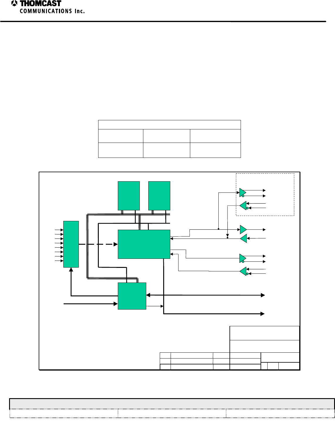
2
Microcontroller Board (MCU) Description - 47266058
COMWAVE DIVISION
All information contained in this document is confidential and proprietary to THOMCAST and shall not be disclosed without the prior written permission of THOMCAST.
CREATED: CPU................................................................12/10/99 CHECKED: KAS ...............................................................1/27/00
RELEASED: PRC
............................................................. 2/10/00
Document #: DOC13-0175
REV: JAN.27.00
Positive analog voltages applied to connector J103 are conditioned and fed to the MCU A/D converter. Single ended
voltages from J103 are amplified and band-limited by op amps contained in U9 and supporting circuitry. The
outputs of these single-ended circuits are fed to A/D inputs. Differential analog voltages are amplified with fixed
gain and band-limited with op amp ICs U10, U14, U17, and supporting circuitry. These op amp circuits convert the
differential input signals to single ended signals. The single ended signals are selected for monitoring through analog
multiplexers. As each signal is selected for monitoring, it is passed to a buffer and finally to an A/D input. All A/D
inputs are protected through voltage and current limiting circuits.
The MCU assembly provides two serial communication ports. Depending on application, either two RS-232 ports or
one RS-232 and one RS-485 port may be required. Jumper JK101 is used to select the function of Port 2. When
JK101 is placed in the 1-2 position, Port 2 is an RS-232 port; in the 2-3 position, it is an RS-485 port.
Table 2: Communication Ports.
Application
Upconverter Local Oscillator System Controller
Port 1- RS-485
Port 2- RS-232 Port 1- RS-485
Port 2- RS-232 Port 1- RS-485
Port 2- RS-485
DRAWN:
RELEASED:
CHECKED:
DWG. NUMBER:
TITLE:
REV: A
A-47266058-034
BLOCK DIAGRAM,
MICRONCONTROLLER BOARD
CPU / 12/99
CPU / 2/9/00
REV Description
KAS / 2/9/00 Scale:
none Sheet
1of 1
COMWAVE DIVISION
ECO#
NAME/DATE
MCU - 68HC812A4
CPLD
RAM FLASH
ROM
To Front Panel
To local
backplane
network
Serial
Serial
address
Data (16)
Signal
Conditioning
Buffering
RS-2321
RS-485
To serial
peripherals
Analog Inputs
A/D in
Logic inputs/
outputs
Logic
In
RS-485
System Controller Only
To ComView
NOTES:
1. When used as system controller, no RS-232
board is used, two RS-485 boards are used.
Figure 1: MCU block diagram.
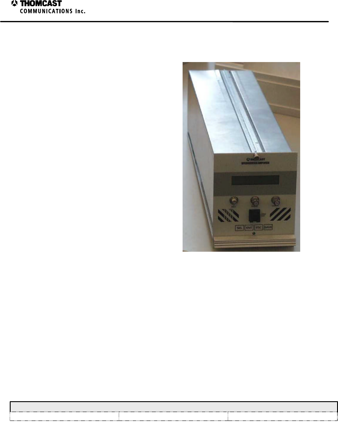
1
Upconverter Plug-In Module Theory of Operation - 47266116
COMWAVE DIVISION
All information contained in this document is confidential and proprietary to THOMCAST and shall not be disclosed without the prior written permission of THOMCAST.
CREATED: AAC................................................................2/4/00 CHECKED: KAS ...............................................................2/7/00
RELEASED: PRC
............................................................. 2/11/00
Document #: DOC14-0039
REV: FEB.07.00
UPCONVERTER PLUG-IN MODULE THEORY OF OPERATION
This plug in module is joined to the main chassis via
three slide rails and two thumbscrews. Several modules
make up this plug-in and are accessible through its two
detachable covers. The covers, together with the rear
panel fan, are part of the forced-convection cooling
system.
The basic function of this plug-in is to convert an IF
input signal to the microwave frequency range,
containing the proper spectrum content and proper
power level to excite subsequent stages of amplification.
To accomplish this, the appropriate level IF signal, local
oscillator signal and power supply voltages must be
delivered to this plug-in. For detailed descriptions on
each of the plug-in modules, see respective module
documentation.
Refer to the block diagram, 47266116-034, for a
functional layout of the modules contained within the
plug-in; refer to Figure 2 and/or Figure 3 for the actual
location of referenced connectors and user accessible
interfaces.
IF and RF signals to and from the plug-in module are
sent through coaxial connectors and cables on the front
and back panels, while signals in a lower frequency
range go through a 48-pin connector located on the
back-panel. IF and RF signals are sent between modules
within the plug-in similarly, via coaxial cables. Signal
traffic other than IF/RF, such as, power supply voltages,
detected power voltages, and serial data from the MCU
board, are distributed between the modules using the
distribution board.
Figure 1: Upconverter plug-in module.
The IF signal enters the plug in and is routed to the IF linear processor where delay and frequency response are
adjusted, as needed. The processed IF signal is then delivered to the microwave converter module, where frequency
conversion takes place; filtering and power amplification follow the conversion inside this module. Embedded
between amplifier stages of the microwave converter module, the microwave pre-corrector generates
intermodulation products with opposite characteristics of those generated in the last amplifiers of the system,
minimizing the overall third and fifth order products of the system RF output. The IPA module provides a final
amplifier stage that boosts the signal before it leaves the plug-in.
Two major level closed loop controls are present in this plug-in module; one is to keep the constant 0dBm total
power at the microwave precorrector module. In this case, a power-sensing device is installed inside the module,
right before the J5 connector, the resultant proportional voltage is then fed to the distribution module where an
integrated circuit (U18) compares with a reference and driver PIN attenuators inside the IF linear processors
accordingly.
The second closed loop control is to compensate the gain variation of the amplifier chain up to the transmitter
output. Both integrators and PIN attenuators are found inside the µW precorrector module and the voltage
proportional to the power level is fed from an external detector module.
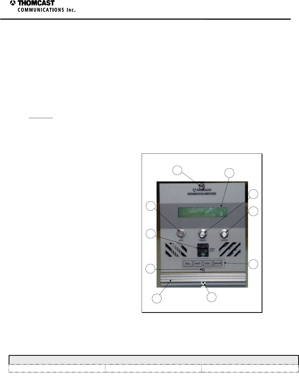
2
Upconverter Plug-In Module Theory of Operation - 47266116
COMWAVE DIVISION
All information contained in this document is confidential and proprietary to THOMCAST and shall not be disclosed without the prior written permission of THOMCAST.
CREATED: AAC................................................................2/4/00 CHECKED: KAS ...............................................................2/7/00
RELEASED: PRC
............................................................. 2/11/00
Document #: DOC14-0039
REV: FEB.07.00
The distribution board also receives the voltage proportional to the temperature that is generated by a temperature
sensor module; this module is usually placed on the last power amplification stage.
The interface board is responsible for providing +24, +12, -12, and +8V to the plug-in, as well as voltages of
forward and reflected detected power for further processing. This board is also the channel through which serial data
is exchanged between this, other plug-ins, and the rest of the system.
The front panel PCB has a serial port, which can be used for testing, adjusting or controlling most of the plug-in
functions with the help of a personal computer. Together the front panel overlay keyboard and the display board
provide a user interface capable of controlling a limited number of functions inside the upconverter plug-in module;
they also allow for the presentation of a series of measurements in the LCD display.
FRONT AND REAR PANEL DESCRIPTIONS
Front Panel
Refer to Figure 2 for numerical references.
1) THUMB SCREWS: Secure module to the
sub-chassis and provide a reliable ground
connection; loosen to remove module for
replacement or repair.
2) LCD DISPLAY: Displays a series of
measurements, user adjustments, and
general status information.
3) LO INPUT: Female SMA 50O connector
used to input the LO signal from the LO
plug-in module. LO level must be 13 dBm
±1 dB.
4) UHF/IF SAMPLE: Female SMA 50O
connector used to test the signal level after
exiting the IF linear processor module.
5) RF SAMPLE: Female SMA 50O
connector used to test the output level.
6) COMM PORT: RS-232 Communications
port for communication to a PC.
7) KEYPAD: User’s selection keys:
a) SEL – select, provides user with
scrolling capabilities.
b) ENT – enter, allows user to choose an
option.
c) ESC – escape, allows user to go back
to previous screen.
d) SAVE – allows user to store new
3
1
9
5
6
2
1
4
87
Figure 2: Upconverter plug-in front panel.
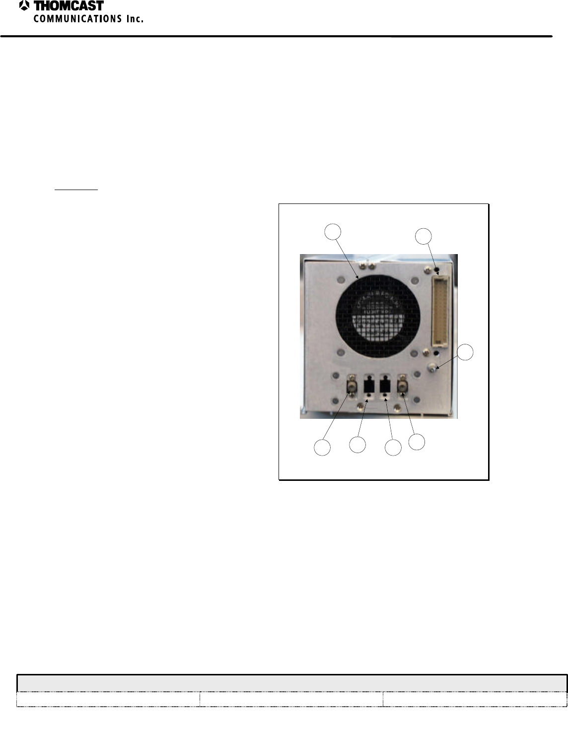
3
Upconverter Plug-In Module Theory of Operation - 47266116
COMWAVE DIVISION
All information contained in this document is confidential and proprietary to THOMCAST and shall not be disclosed without the prior written permission of THOMCAST.
CREATED: AAC................................................................2/4/00 CHECKED: KAS ...............................................................2/7/00
RELEASED: PRC
............................................................. 2/11/00
Document #: DOC14-0039
REV: FEB.07.00
settings or adjustments.
8) POTENTIOMETER: Used in conjunction with the LCD display and keypad this allows the following user
adjustments:
a) Power Level
b) Output Power
c) Frequency Response 1
d) Frequency Response 2
e) Precorrection
i) Distribution Generation
ii) Cancellation 1
iii) Cancellation 2
iv) Phase
9) HANDLE: Assists in removing module from sub chassis.
Rear Panel
Refer to Figure 3 for numerical references.
1) FAN: 18 CFM DC for plug-in module
cooling only.
2) 48 PIN DIN: Interface to the back plane,
(all power, control and diagnostics)
3) GROUND / ALIGNMENT STUD:
Ensures that proper ground is made prior
to engaging the 48 pin DIN; also aids in
the alignment of the module within the
sub-chassis.
4) IF INPUT: Male 50O blind mate
provides interface to the back plane and
allows passage for the IF input signal.
5) Not applicable in this model.
6) Not applicable in this model.
7) RF OUTPUT: Male 50O blind mate
supplies the RF output signal to the
transmitting system of amplifier cage,
depending on model type.
3
57
2
1
4
6
Figure 3: Upconverter plug-in rear panel.

1
Upconverter Plug-In Module Specifications – 47266117.00
COMWAVE DIVISION
All information contained in this document is confidential and proprietary to THOMCAST and shall not be disclosed without the prior written permission of THOMCAST.
CREATED: AAC................................................................3/19/99 CHECKED: KAS ...............................................................2/7/00
RELEASED: AAC
............................................................. 2/8/00
Document #: 47266117.00-306
REV: P1
SPECIFICATIONS SUBJECT TO CHANGE WITHOUT NOTICE
UPCONVERTER PLUG-IN MODULE SPECIFICATIONS
Parameter Specification Notes/Test Conditions
IF INPUT
Digital
Average Input Power -15 dBm ± 2 dB 223-1 PN data sequence (at transmitter output)
IF Input Frequency 44 MHz (center) Other frequency options available
Connector / Impedance Blind Mate / 75 O Mates with floating back-plane connector
Analog (Combined visual and aural)
IF Input Level -8 dBm peak ± 2 dB (Visual
Carrier)
-23 dBm peak ± 2 dB (Aural
Carrier)
Combined visual and aural
IF Input Frequency
Aural Carrier
Visual Carrier 41.25MHz
45.75MHz
Other frequency options available
Connector / Impedance Blind Mate / 75 O Mates with floating back-plane connector
RF OUTPUT
Digital
Average Output Power 20mW to 200mW Function of A.L.C. settings - 223-1 PN data sequence (at
driver output)
Output Frequency 1850 - 3600 MHz In select bands
Frequency Response ≤ ±0.25 dB FC ±2.6 MHz
Measured at Sub-rack output
IM3 (dBc) < 50 16dBm RF Output Power (64QAM) Relative to in-band
average PSD measured @ 100 KHz RBW
Carrier to Noise (C/N) ≥ 55 dB
Hum and Noise ≤ -60 dBc
Group Delay ≤ ±15 ns FC ±2.6 MHz
RF Output Connector
Digital Modulation
Error Vector Magnitude (EVM) ≤ 2.0% 64-QAM/8-VSB @ 5.06 Msps RMS average over 12,500
symbols
Measured at Sub-rack output
Digital Modulation
Signal to Noise Ratio (SNR) ≥ 30 dB 64-QAM/8-VSB @ 5.06 Msps RMS average over 12,500
symbols
Measured at Sub-rack output
Magnitude Linearity
(AM-AM conversion) ≤ ±0.125 dB Measured at Sub-rack output
Phase Linearity
(AM-PM conversion) ≤ ±0.75°Measured at Sub-rack output
RF Output Regulation ≤ ± .2 dB Measured at Sub-rack output
Connector / Impedance Blind Mate / 50 O Mates with floating back-plane connector
Analog Performance
Output Power 100mW - 1 Watt Peak Sync Adjustable from 10 to 100% of peak sync power
Output Frequency Any 6, 7, or 8 MHz Channel
1850 - 3600 MHz In select bands
Emission 5M75C3F or per CCIR

2
Upconverter Plug-In Module Specifications – 47266117.00
COMWAVE DIVISION
All information contained in this document is confidential and proprietary to THOMCAST and shall not be disclosed without the prior written permission of THOMCAST.
CREATED: AAC................................................................3/19/99 CHECKED: KAS ...............................................................2/7/00
RELEASED: AAC
............................................................. 2/8/00
Document #: 47266117.00-306
REV: P1
SPECIFICATIONS SUBJECT TO CHANGE WITHOUT NOTICE
Parameter Specification Notes/Test Conditions
IM3 (dBc) < 50 Two Tones @ 13dBm/c (∆f = 6MHz) – RF Output
Connector
RF Output Regulation = ± 0.2 dB
DC POWER REQUIREMENTS
Voltages / Currents +12 VDC ±.5 @ 2.5A max
+8 VDC ±.5 @ 1.2A max
-12 VDC ±.5 @ 150ma max
Connector 48 conductor, 3amps / circuit
minimum Interfaces to back-plane
ENVIRONMENTAL
Cooling Forced air-cooled, minimum of 18
CFM required Forced air-cooled drawing ambient air through the intake
on the front of the Up-Converter Plug-In. and exhausting
out the rear.
Operating Temperature 0°C to 50°C
Relative Humidity 0 to 95% non-condensing
ALARMS / INDICATORS / AJUSTMENTS / CONTROLS
RF Output Failure Alarm DRIVER FAILURE Low (TTL
Low) = RF Output Failure Signal available at back-plane
Over- Temperature Alarm DRIVER FAILURE Low (TTL
Low) = Over Temperature Signal available at back-plane and
Visible via LCD Display (Software/pending)
In-Signal Indicator PRESENT or NOT PRESENT Visible via LCD Display (Software/pending)
Transmit Indicator ON AIR or OUT OF AIR Visible via LCD Display (Software/pending)
Power Supply Status /
Measurements PASS or FAIL / V scale Visible via LCD Display (Software/pending)
RF Power Measurements % Scale (dBm scale option) Visible via LCD Display (option is Software/pending)
Temperature Indicator °C scale Visible via LCD Display (Software/pending)
Frequency Response (low side)
Adjustment Potentiometer allows adjustment of
low side IF frequency response Access via front panel
Frequency Response (high side)
Adjustment Potentiometer allows adjustment of
high side IF frequency response Access via front panel
Distortion Level Adjustment Potentiometer allows adjustment of
pre-distortion level Access via front panel
ALC Level Adjustment Potentiometer allows adjustment of
ALC. Access via front panel
Detector Threshold Control RS-232 interface Set via laptop computer with VB application, Access via
front panel
Input Level Control RS-232 interface Set via laptop computer with VB application, Access via
front panel
Frequency Response (low side)
Control RS-232 interface Set via laptop computer with VB application, Access via
front panel
Frequency Response (high side)
Control RS-232 interface Set via laptop computer with VB application, Access via
front panel
Distortion Level Control RS-232 interface Set via laptop computer with VB application, Access via
front panel
Linearity Cancellation 1 Control Potentiometer allows adjustment of
linearity cancellation Access via front panel
Linearity Cancellation 2 Control RS-232 interface Set via laptop computer with VB application, Access via
front panel

3
Upconverter Plug-In Module Specifications – 47266117.00
COMWAVE DIVISION
All information contained in this document is confidential and proprietary to THOMCAST and shall not be disclosed without the prior written permission of THOMCAST.
CREATED: AAC................................................................3/19/99 CHECKED: KAS ...............................................................2/7/00
RELEASED: AAC
............................................................. 2/8/00
Document #: 47266117.00-306
REV: P1
SPECIFICATIONS SUBJECT TO CHANGE WITHOUT NOTICE
Parameter Specification Notes/Test Conditions
Distortion Phase Control RS-232 interface Set via laptop computer with VB application, Access via
front panel
ALC Level Control RS-232 interface Set via laptop computer with VB application, Access via
front panel
Stand-by Control RS-232 interface Set via laptop computer with VB application, Access via
front panel
Reset Control Momentary switch to reset on-
board Microprocessor Access via front panel
Function Switch
Stand-by
Meter Off
+11V P.S.
FWD PWR
REFL PWR.
Places system in stand-by mode
No indication on analog meter
Displays proper DC voltage of the
main switching power supply
Displays forward power on analog
meter
Displays reflected power on analog
meter
Access via front panel
Analog Meter
+11V P.S.
FWD PWR
REFL PWR
Indicates proper DC voltage of the
main switching power supply
Indicates forward power
transmitted
Indicates reflected power
transmitted
Visible via front panel
PHYSICAL
Mechanical Dimensions 4.75”H x 4.2”W x 17.5”D1
12.07 cm H x 10.67 cm W x 44.45 cm D
Weight 6 lbs. (3Kg)
Front Panel Color Matches Sherwin William’s Paint
No.
Light Gray ……..F63TXA2555
Medium Gray ….F63TXA4841
Paint mix number 4303 identifies store location when
added to Paint No.
Lexan overlay color matched as indicated
1 Measured without ground pin on rear panel and front panel handle; add approximately 2” for these.
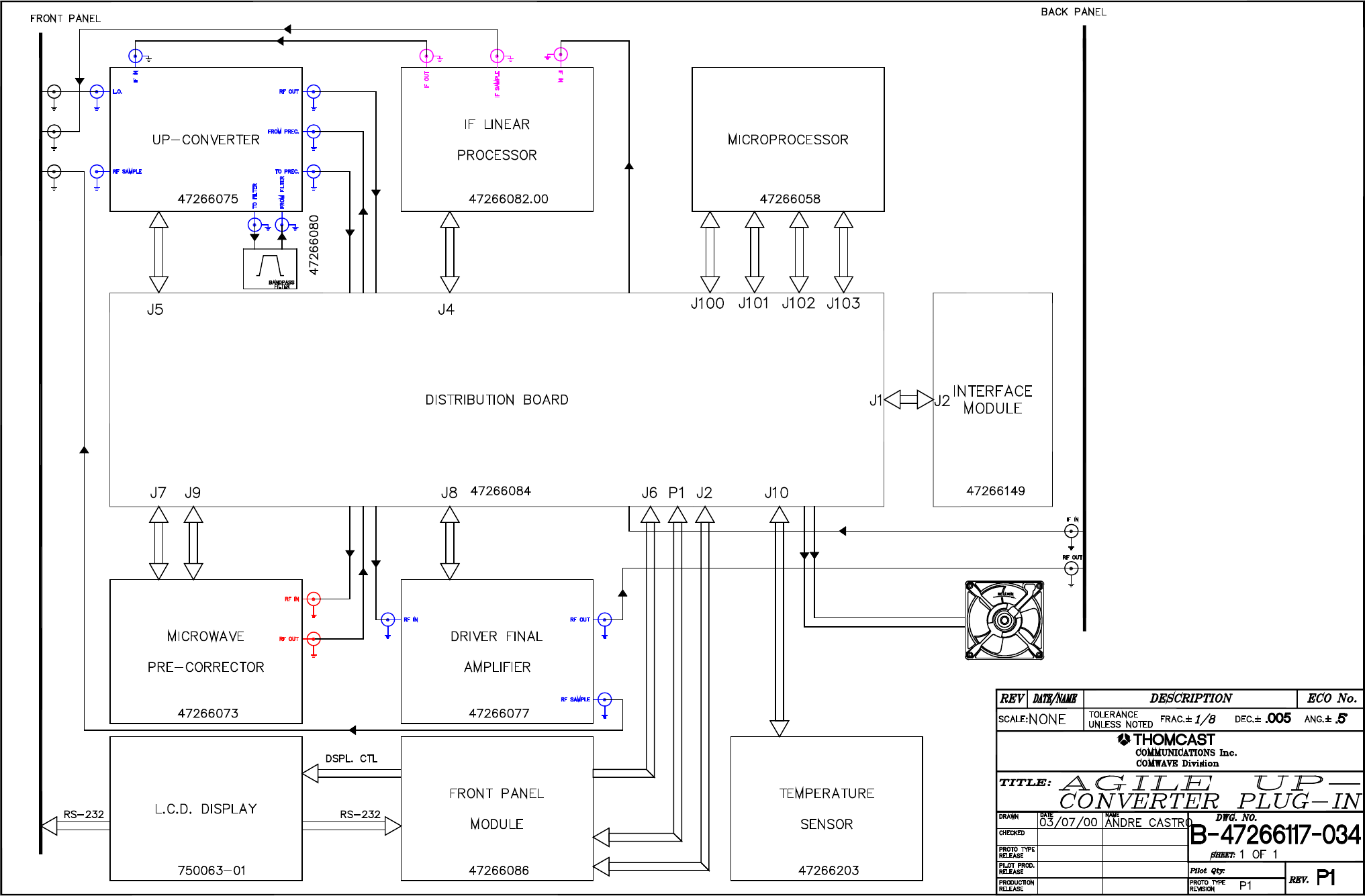
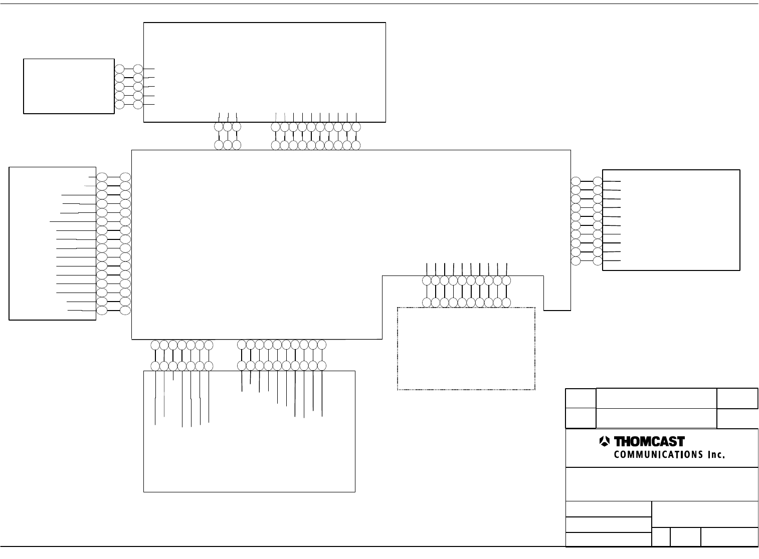
Microwave Precorrector - 47266073
Front Panel Board - 47266086
Distribution board - 47266084
AGND
AGND
AGND
VGS_MON_2
VGS_MON_3
-12V
IPA_DETECTED_PWR
DRIV_FIN_AMP_CURR
GND
AGND
DRIVER_RF_MEASURE
NC
NC
+12V
1
2
3
4
5
6
7
1
2
3
4
5
6
7
8
9
10
+12v
LCD Display board - 750063
DIGITIAL GND
+5VDIGITAL
VDC
D5
RS
R/W
E
D0
D1
D2
D3
D4
D6
D7
LED +
LED -
1
2
3
4
5
6
7
8
9
10
11
12
13
14
15
16
1
2
3
4
5
6
7
8
9
10
11
12
13
14
15
16
1
2
3
4
5
6
7
1
2
3
4
5
6
7
8
9
10
1
2
3
4
5
6
7
8
9
10
Microwave
Converter
47266075.00
VGS_MON_1
MIX_AMP_CURR
-12V
AGND
UW_CONVERTER_PWR
OUT_AMP_CURR
RF_CORR_DET_IN
AGND
1
2
3
4
5
6
7
8
9
10
OUT_AMP_CURR
INTER_AMP_CURR
DRAWN:
RELEASED:
CHECKED:
DWG. NUMBER:
TITLE:
REV: P1
A-47266117-050
INTERCONNECT, AGILE U/C
PLUG-IN MODULE
AAC 02/14/00
Name / date
???????? Scale:
none Sheet
1 of 2
COMWAVE DIVISION
REV Description ECO#
NAME/DATE
1
2
3
DIGITAL GND
+5V DIGITAL
NC
1
2
3
P1
P1
1
2
3
4
5
6
7
8
9
10 USERPOT
SELECT
RS232_TXD
RS232_RXC
ENA_RS232
CH
EN
SAVE
ESC
ENTER
1
2
3
4
5
6
7
8
9
10
J2 P2
1
2
3
4
5
DIGITAL GND
SELECT
ENTER
ESC
SAVE
1
2
3
4
5
P3
Front Panel
Overlay -
47266003
P1P1
P2P2
J6
J5
P1
DRIV_FIN_AMP_CURR
DRIV_FIN_AMP_CURR
1
2
3
4
5
6
7
8
9
10
1
2
3
4
5
6
7
8
9
10
P1
J8
IPA -
47266077.00
ADAPT_CANCEL
ALC_INT_EXT_CTRL
PWR_LIMIT
ALC_MAN_CTRL
PHASE
CANC2
DIST_GEN
CANC1
ALC_ON_OFF
ALC_AUTO_CTRL
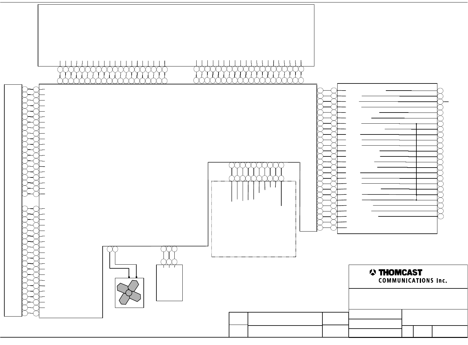
Distribution board - 47266084
ENCODER_GAIN_CTL
+12V
NC
GND
RS485_LOCAL_T-
FWDPWR_1
REMOTE_SHDN
GND
BOOSTER_INSIGNAL
+8V
+12V
+24V
RS485_LOCAL_R-
RS485_LOCAL_T+
RFLTDPWR_1
+8V
+12V
IF Linear Processor -
47266082.00
AGND
AGND
IF_THRESHOLD
IF_ATT
NC
FREQ_RESP#2
+12VA
AUX_ATT_2
FREQ_RESP#1
+12VA
DRAWN:
RELEASED:
CHECKED:
DWG. NUMBER:
TITLE:
REV: P1
A-47266117-050
AAC 02/14/00
Name / date
???????? Scale:
none Sheet
2 of 2
COMWAVE DIVISION
REV Description ECO#
NAME/DATE
GND
+5VA
TEMPERATURE
1
2
3
1
2
3
Temperature Sensor
- 47266203
1
2
Fan
1
2
3
4
5
6
7
8
9
10
1
2
3
4
5
6
7
8
9
10
J4P1
1
2
3
4
5
6
7
8
9
10
11
12
13
14
15
16
17
18
19
20
21
22
23
24
25
26
1
2
3
4
5
6
7
8
9
10
11
12
13
14
15
16
17
18
19
20
21
22
23
24
25
26
J2J1
IN_SIGNAL
-12V
RS485_LOCAL_R+
GND
GND
AGC_LEVEL
DRIVER_FAULT
NC
NC
1
2
3
4
5
13
14
16
17
18
19
20
21
22
29
32
33
34
35
36
41
44
45
48
GND
Interface Board - 47266149
J1
DRIV_FIN_AMP_CURR [3,4]
1
2
3
4
5
6
7
8
9
10
11
12
13
14
15
16
17
18
19
20
GND
SYS_FWD_DET_PWR [4]
SYS_RFL_DET_PWR [2,4]
USER_POT [5]
ADAPT_CORR [5]
VDD_IO [3]
OUT_AMP_CURR [3,4]
DRIVER_RF_MEAS [4]
+8v [3.5]
MIX_AMP_CURR [3,4]
INTER_AMP_CURR [3,4]
AGC_LEVEL [4,5]
ADAPT_CANCEL [4]
TEMP [3]
VGS_MON_1 [4]
VGS_MON_2 [4]
VGS_MON_3 [4]
8VSW [3]
1
2
3
4
5
6
7
8
9
10
11
12
13
14
15
16
17
18
19
20
DAC_2_CS [1]
1
2
3
4
5
6
7
8
9
10
11
12
13
14
15
16
17
18
19
20
GND
DO [5]
D1 [5]
D2 [5]
D3 [5]
DAC_1_CS [1]
D7 [5]
DAC_3_CS [1]
D4 [5]
D5 [5]
D6 [5]
AGC_ON_OFF [2]
ALC_ON_OFF [2]
AGC_INT_EXT_CTRL [2]
ALC_INT_EXT_CTRL [2]
EN [5]
RS [5]
R/W [5]
1
2
3
4
5
6
7
8
9
10
11
12
13
14
15
16
17
18
19
20 E [5]
J102
J103
Microcontroller Board - 47266058.00
DRIVER_FAULT [5]
1
2
3
4
5
6
7
8
9
10
11
12
13
14
15
16
17
18
19
20
GND
ENTER [5]
ESC [5]
CH [5]
ENA_RS232 [5]
ENCODER_GAIN_CTRL [5]
REMOTE_SHDN [5]
SAVE [5]
SELECT [5]
IN_SIGNAL [4,5]
FST_RLCTD_SHTD [2]
SS [1]
LC_DAC [1]
MOSI [1]
CLOCK [1]
SUPPLIES_EN [3]
1
2
3
4
5
6
7
8
9
10
11
12
13
14
15
16
17
18
19
20 ALC_LOOP_SELECT_2 [2,4]
J101
1
2
3
4
5
6
7
8
9
10
11
12
13
14
15
16
17
18
19
20
GND
RS485_LOCAL_R- [5]
RS485_LOCAL_T+ [5]
RS485_LOCAL_T- [5]
RS485_LOCAL_R+ [5]
RS232_TXD [5]
RS232_RXD [5]
-12V [3,4,5]
+12VA [2,3,4,5]
1
2
3
4
5
6
7
8
9
10
11
12
13
14
15
16
17
18
19
20 +12VA [2,3,4,5]
J100
Microcontroller Board - 47266058.00
INTERCONNECT, AGILE U/C
PLUG-IN MODULE

1
Microwave
Precorrector Module – 47266073
COMWAVE DIVISION
All information contained in this document is confidential and proprietary to THOMCAST and shall not be disclosed without the prior written permission of THOMCAST.
CREATED: AAC................................................................01/31/00 CHECKED: KAS ...............................................................02/02/00
RELEASED: PRC
............................................................. 2/11/00
Document #: DOC13-0177
REV: FEB.02.00
MICROWAVE PRECORRECTOR MODULE
Built in a 3” X 6” housing, this module consists of two compartments: a RF and DC & Control section; they are
placed in opposite sides of the housing. Two harnesses, a seven and ten conductor, reach the interior of the module
on the control side.
RF Section:
This section is implemented essentially by microwave broadband amplifiers (U1-U4 and U6-U7) and
hybrids (HYB1-HYB7). All amplifiers are biased through resistors from the only power supply voltage and
use quarter-wavelength transformers and a capacitor for de-coupling.
DC and Control Section:
A variety of electronic components are used to control the RF signal processing that takes place in the RF
section. Externally accessible potentiometers and switches allow adjustments and changes in the module
modes of operation.
Correction is performed by subtraction of a pre-generated distortion from the one present at the output of the system.
A RF input signal at about 0dBm-power level is applied to J1. This signal is amplified and split two ways; one goes
through a linear path while the other goes through the circuitry that generates the desired pre-distortion. Both signals
are combined and amplified to recover the losses of their processing. Finally, the signal goes through the broadband
attenuator that performs the ALC and is routed out the module through J2. Table 1 summarizes each control
accessible from the top of the module. Module control through external voltages delivered via connector P2 is also
possible.
Table 1: Microwave precorrector adjustment controls.
NUMERICAL
REFERENCE NAME FUNCTION
1J1 RF Input
2J2 RF Output
3AUTO / MAN Switch Sets the power control mode
4D.G. Control for pre-distortion signal amplitude
5CANC1 Module internal cancellation adjustments
6CANC2 Module internal cancellation adjustments
7PH. ADJ Adjust the phase of the pre-distortion
8AUTO Adjust output power in ALC mode
9MAN Adjust output power in manual mode
10 PWR LMTR Adjust maximum output power achievable by the system
11 PC ON / OFF Sets pre-correction On or Off
12 P1 +12V, ALC voltage (connector)
13 P2 External voltages for adjustments (connector)
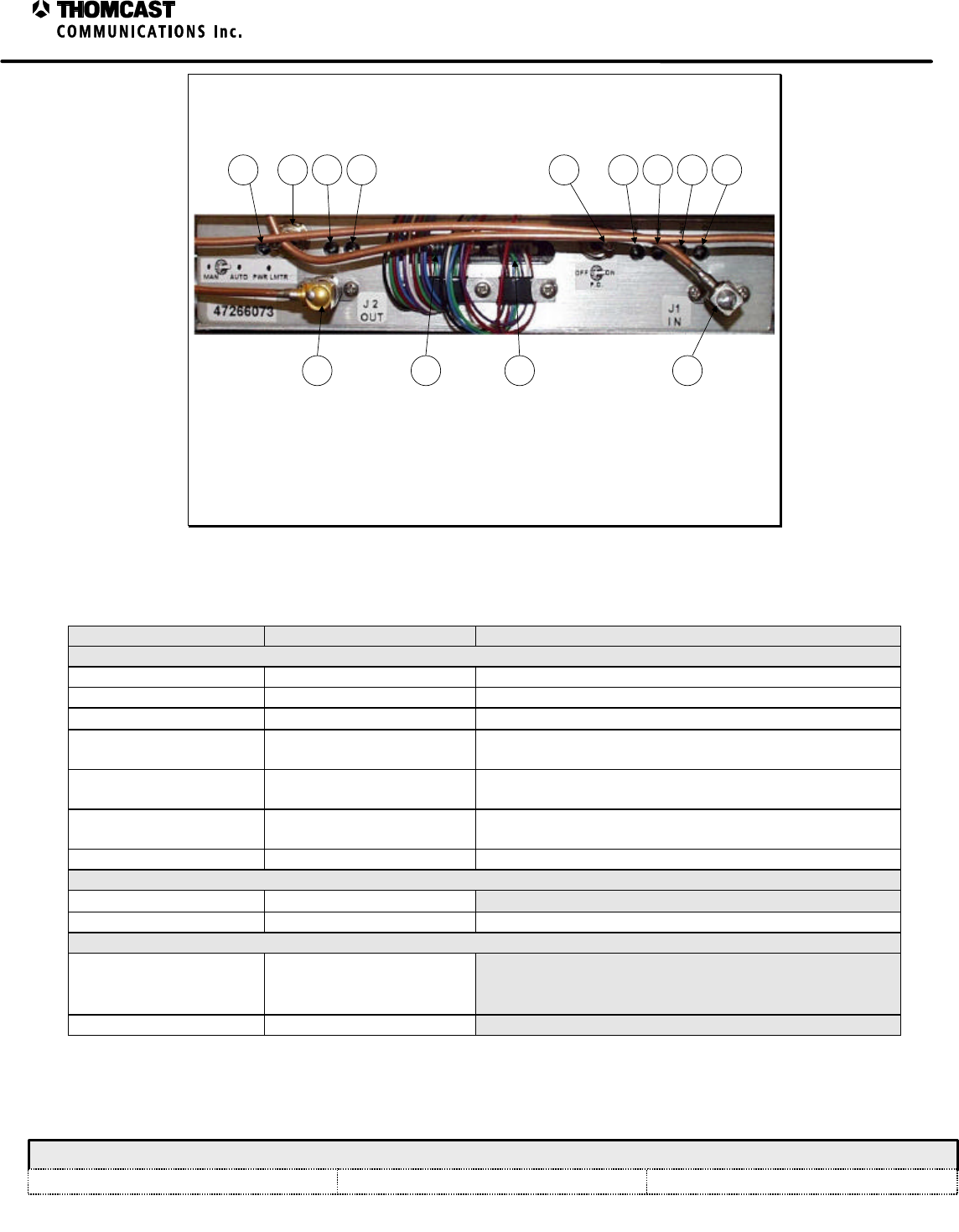
2
Microwave
Precorrector Module – 47266073
COMWAVE DIVISION
All information contained in this document is confidential and proprietary to THOMCAST and shall not be disclosed without the prior written permission of THOMCAST.
CREATED: AAC................................................................01/31/00 CHECKED: KAS ...............................................................02/02/00
RELEASED: PRC
............................................................. 2/11/00
Document #: DOC13-0177
REV: FEB.02.00
9 3 8 10
2 113 12
11 5 6 7 4
Figure 1: 47266073 microwave precorrector.
Table 2: Specifications.
Parameter Specification Notes/Test Conditions
RF
Gain -8 dB min / 3 dB max 1.8 to 3.6 GHz (function of ALC)
Input Return Loss < -10 dB 1.8 to 3.6 GHz
Total Flatness ± 3 dB 1.8 to 3.6 GHz
Power Limiter Pmax = nominal power +1
dB ALC on or off
Distortion Generation -60 dBc to -32 dBc 1.8 to 3.6 GHz
1 carrier, 64 QAM, spectrum analyzer @ 100 KHz RBW
Cancellation >25 dBc 1.8 to 3.6 GHz
1 carrier, 64 QAM, spectrum analyzer @ 100 KHz RBW
Phase Range >45º adjustment 1.8 to 3.6 GHz
DC
Power Supply 12 ± 0.5 V
Current .6 A S21 = 2dB; Maximum pre-distortion
GENERAL
Impedance / Connector
Input
Output 50 Ω / Female SMA
50 Ω / Female SMA
Operating Temperature 0° C to 50° C
• SPECIFICATIONS ARE SUBJECT TO CHANGE WITHOUT NOTICE.
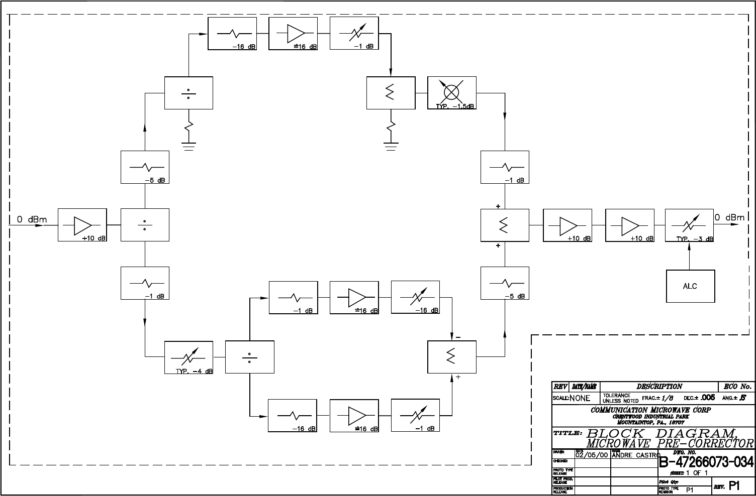

1
Upconverter Plug-In Module, MCU State Machine
Firmware Description – 47266058.00
COMWAVE DIVISION
All information contained in this document is confidential and proprietary to THOMCAST and shall not be disclosed without the prior written permission of THOMCAST.
CREATED: CPU................................................................1/10/00 CHECKED: KAS ...............................................................2/9/00
RELEASED: PRC
............................................................. 2/11/00
Document #: DOC13-0187
REV: FEB.09.00
UPCONVERTER PLUG-IN MCU STATE MACHINE,
FIRMWARE DESCRIPTION
The MCU assembly and its firmware monitor various parameters, conditions, and commands in the plug-in module.
The firmware uses the pass/fail states of the parameters to determine the operating state of the plug-in.
In the normal AUTO mode of operation, the operating state of the plug-in is used to determine the control settings
for the plug-in. Following a RESET, the firmware enters an INIT (initialization) state, in which the initialization of
registers and network operations is performed, DOC13-0188 discusses this in more detail. Following INIT, the plug-
in enters the STANDBY state. In STANDBY, the RF power output of the upconverter plug-in is disabled, and
settings for the various internal modules are set for minimum gain.
Unless commanded to remain in STANDBY, the plug-in will enter the STABILIZE state, allowing the unit to come
up to desired operating power without transient failures. After a short stabilization period, the plug-in enters the
OPERATE state. In this state, full output power is produced, and pre-correction and gain controls are operational.
As the conditions of the measured parameters change, the state is modified accordingly. For example, if signal
presence is lost, the plug-in will enter the STANDBY state and will remain in that state until the signal returns. Once
signal returns, if no other failure conditions exist, the plug-in will transition through STABILIZE to the OPERATE
state. If a reflected power sample is found outside of the passing range while the plug-in is in OPERATE, the state is
changed to LIMP to attempt to provide reduced output power, thereby reducing the reflected power.
Other failures that may result in unsafe operation or damage to the plug-in or system cause the plug-in to enter the
FAILED state. The firmware may perform multiple tests of a failing parameter before deciding to enter FAILED to
reduce the effects of transients. In the FAILED state, RF output power and DC supply to the plug-in output
amplifiers are disabled. The firmware cannot exit the FAILED state without user intervention.
During factory calibration or customer site installation, the plug-in may be operated in MANUAL mode. In
MANUAL mode, the operating state is continually updated, but the state is not used to determine the control settings
of the plug-in. The control settings remain set as they were when the MANUAL mode was entered until overridden
by user commands. The user may adjust key plug-in settings to optimize plug-in performance and modify behavior,
and the settings may be stored in non-volatile memory or discarded.

1
Upconverter Plug-In Firmware Description – 47266116.00
COMWAVE DIVISION
All information contained in this document is confidential and proprietary to THOMCAST and shall not be disclosed without the prior written permission of THOMCAST.
CREATED: CPU................................................................1/10/00 CHECKED: KAS ...............................................................2/9/00
RELEASED: PRC
............................................................. 2/11/00
Document #: DOC13-0188
REV: FEB.09.00
UPCONVERTER PLUG-IN FIRMWARE DESCRIPTION
The microcontroller (MCU) assembly and its operating program (firmware) handle internal monitoring functions in
the plug-in. The flow of execution of the program used in this chassis is described below. The firmware program is
contained in non-volatile memory on the MCU board.
The firmware begins execution after a RESET or power-up. The firmware instructs the MCU to initialize various
MCU registers and hardware ports, including the A/D converter. Following this, a lamp test operation is performed.
All chassis front panel LED’s are illuminated for approximately 1 second then darkened. The lamp test allows a
quick verification that all front panel LED’s are functioning. In addition, the lamp test is a clear outward sign that
the MCU board is receiving power, is executing the firmware program, and has recovered from RESET. Shortly
after the lamp test, the LED’s will display chassis status as determined by firmware tests.
Following the lamp test, program variables and measurement records are initialized. The initialization assures
integrity of records used to hold test data and communication messages. Following the initialization, the firmware
starts the MCU network functions. This process configures the MCU communication port, and instructs the MCU
how handle incoming messages. The firmware also checks an internal memory register to determine whether an RS-
485 network node address for this MCU assembly has been set. The network node address will either be the value
found in this register, or if no value has been set, a default value.
All aforementioned tasks are performed once after RESET. Following these tasks, a program loop is entered that
handles monitoring and communications tasks, as described below. The loop may be temporarily interrupted by
incoming communication messages. RESET ends the loop and restarts program execution.
The firmware determines the condition of key parameters such as reflected power and signal presence by taking
samples of signals of interest applied to the MCU board. Analog signals are measured using the MCU A/D
converter, while logic inputs are monitored with either the MCU or CPLD . The samples are tested against
numerical limits, and a pass/fail status is determined for each monitored signal. The firmware uses the pass/fail
states of the parameters to determine the operating state of the plug-in. The operating state of the plug-in is used to
determine the control settings for the plug-in. See documents DOC13-0187 and DOC21-0021 for a description of
the firmware state machine and its effect on the control of the plug-in.
The measurements of parameters and other operating information (status) are compiled by the firmware in a
memory table. This status table may be sent as a communication message to the System Controller or to a PC-based
user interface application. The System Controller or the user application sends a status query message to the plug-in
and receives the status table in response.
At any time during firmware execution, a communication message may be received by the MCU. This results in an
interruption of program execution, allowing the firmware to quickly collect and store the incoming message.
Firmware execution then returns to the point following the interruption. After a complete message has been
collected by the firmware, a response is constructed by the firmware and sent by the MCU under firmware
command.
In addition to the status query, other commands may be issued to the plug-in:
• STANDBY command - causes output power to be disabled
• ON AIR command - re-enables the plug-in output power
• RESET command - causes the firmware to restart execution
Additional commands are used during factory alignment and customer site installation to optimize equipment
performance. The commands provide calibration settings that are stored by the MCU in non-volatile memory. The
calibration settings are accessed during firmware operation to set the various plug-in systems into the calibrated
operating condition after a RESET.

1
LO Plug-In Module Theory of Operation
COMWAVE DIVISION
All information contained in this document is confidential and proprietary to THOMCAST and shall not be disclosed without the prior written permission of THOMCAST.
CREATED: DMW..............................................................3/8/00 CHECKED: KAS ...............................................................3/8/00
RELEASED: DMW
........................................................... 3/8/00
Document #: DOC14-0038A
REV: MAR.08.00
LO PLUG-IN MODULE THEORY OF OPERATION
The LO plug-in module is superceded by the
Agile Synthesizer Drawer in the application.
Please refer to the manual for the Agile
Synthesizer Drawer, DOC33-0037 for a
discussion of the LO. Figure 1: Agile Synthesizer Drawer.
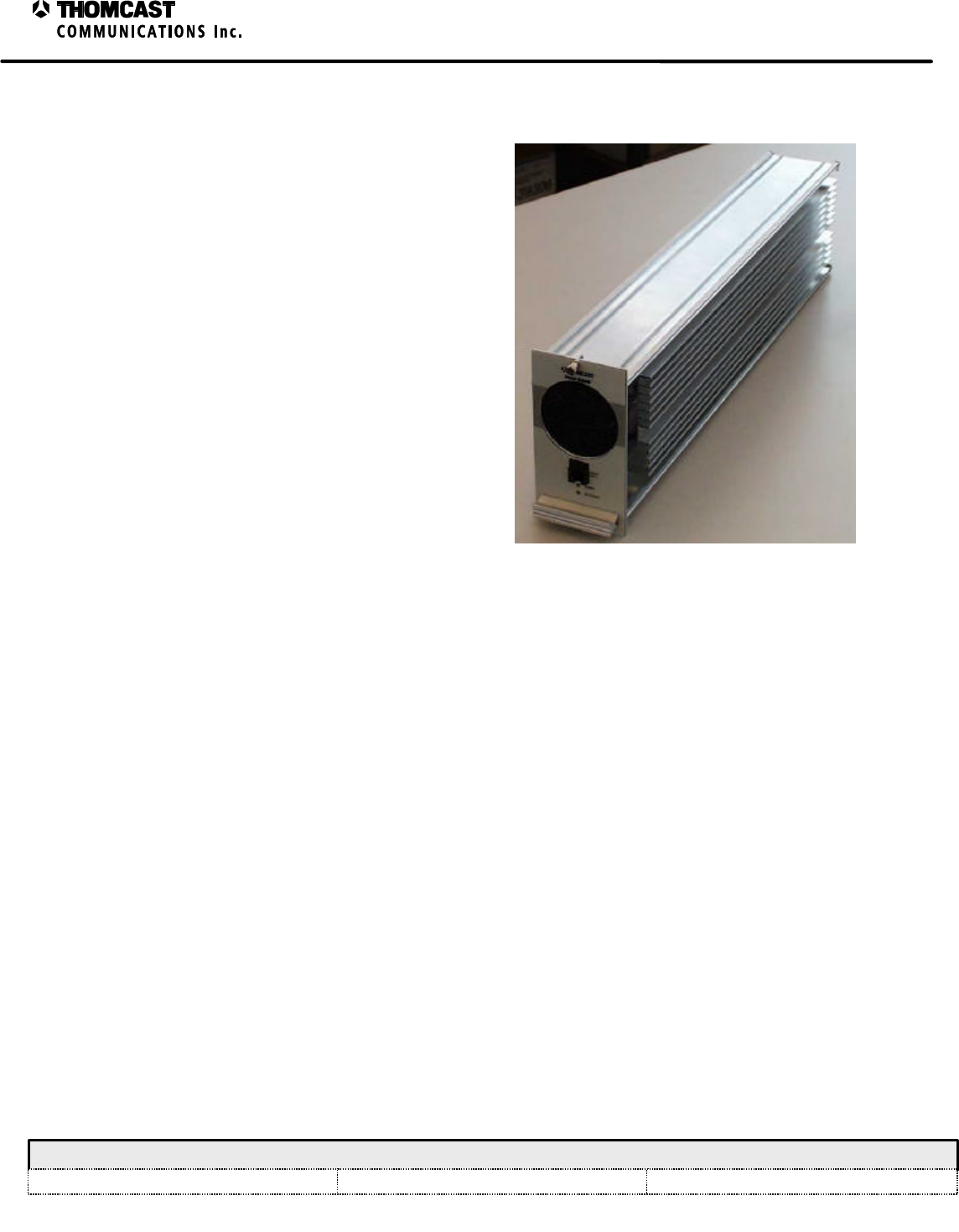
1
Power Supply Module Theory of Operation - 47266099
COMWAVE DIVISION
All information contained in this document is confidential and proprietary to THOMCAST and shall not be disclosed without the prior written permission of THOMCAST.
CREATED: CTS ................................................................1/26/00 CHECKED: KAS ...............................................................1/27/00
RELEASED: PRC
............................................................. 2/11/00
Document #: DOC14-0036
REV: JAN.27.00
POWER SUPPLY MODULE THEORY OF OPERATION
The power supply module uses the latest technology and
is equipped with the following features:
• Single-chip embedded microcontroller
monitoring and control.
• RS-232 front panel connector for quick
interface to desktop computer.
• Modular, hot swap assembly.
The above features offer quick and simple monitoring
functions and provide expedient assembly and repair
time.
Figure 1: Plug-in power supply module.
The DC power supply module receives 48 VDC from an external front end power supply and converts it into the
working voltage and power requirements necessary to operate the driver. Additionally, the power supply houses the
system controller CPU card that organizes network messages between the driver modules, power amplifier
segments, and the ComView monitor and control system. See DOC13-0175 for a more detailed discussion of the
system controller card, DOC13-0185 for a discussion of the system controller cards firmware, and DOC13-0173 for
a discussion of the embedded controller.
The power supply module contains a single chip embedded controller, it constantly monitors the performance of the
power supply and external controls. The embedded controller processes this information and decides the operational
control of the module then informs the system controller of the power supply's operational status.
The power supply is cooled by a single fan, and is mounted in an extrusion designed to dissipate the heat generated
from the components within. The fans of the sub-chassis also ventilate the power supply plug-in module; for
additional protection, the embedded controller monitors the temperature of the plug-in. If the plug-in module is
operating over temperature, controlled shut down of the power supplies within will occur.
The plug-in module consists of three circuit boards, the converter board with the embedded controller, system
controller board, and display board, which needs no further explanation. A brief discussion of each board's task(s)
follows:
The core of the module is the DC converter PCB. The DC converter board mounts overtop a DC to DC
converter module, which transforms the 48VDC input voltage into +12VDC. The DC converter PCB
produces the remaining voltages needed to operate the driver from the 12 VDC.
The embedded controller mounted on the DC converter PCB, monitors the voltages and currents from the
power supply and controls the output based upon voltage and current measurements. It will switch off the
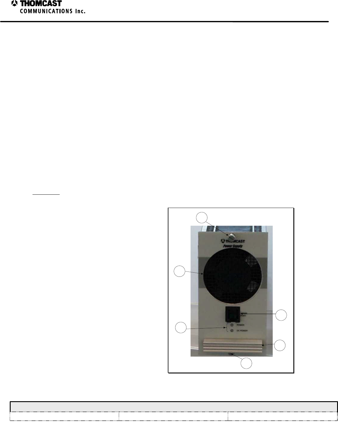
2
Power Supply Module Theory of Operation - 47266099
COMWAVE DIVISION
All information contained in this document is confidential and proprietary to THOMCAST and shall not be disclosed without the prior written permission of THOMCAST.
CREATED: CTS ................................................................1/26/00 CHECKED: KAS ...............................................................1/27/00
RELEASED: PRC
............................................................. 2/11/00
Document #: DOC14-0036
REV: JAN.27.00
positive voltages to the driver when a loss of negative voltage is detected in order to protect amplifier
devices that are located within the upconverter / amplifier plug-in.
Mounted directly above the DC converter PCB is the system controller PCB. It receives its operating
power directly from the DC converter PCB. Additionally, the DC converter PCB routes the RS-485
communication networks between the system controller to the back plane connector in the rear of the
chassis and eventually to other modules within the driver, as well as the ComView monitoring system.
The power supply module can be divided into the following five major categories:
1. The power supplies provide the operating voltages needed to power the driver.
2. The power supply enables turn the power supply voltages on and off when commanded by the embedded
controller.
3. The current and voltage monitoring circuit samples the operating parameters of each power supply and
conditions them into the required voltage range within the analog to digital converters of the embedded
controller.
4. A temperature sensor provides input to the microcontroller proportional to the ambient temperature of the
module.
5. The embedded controller controls and monitors the performance of the module.
More detailed discussions of the above categories can be found in subsequent documents.
FRONT AND REAR PANEL DESCRIPTIONS
Front Panel
Refer to Figure 2 for numerical references.
1) COMM PORT: RS-232 Communications
port for communication to a PC.
2) LED's: Status monitoring LED's which
provide visual indication of operating
parameters.
a) Power
i) GREEN = receiving power from
the front end power supply
ii) UNLIT = no power from the front
end power supply
b) DC Power
i) GREEN = output power is present
ii) UNLIT = no output power
3) FAN: 18-CFM DC for plug-in module
cooling only.
4) THUMB SCREWS: Secure module to the
sub-chassis and provide a reliable ground
connection; loosen to remove module for
replacement or repair.
5) HANDLE: Assists in removing module
from sub chassis.
1
3
2
5
4
4
Figure 2: Power supply module front panel.
3
Power Supply Module Theory of Operation - 47266099
COMWAVE DIVISION
All information contained in this document is confidential and proprietary to THOMCAST and shall not be disclosed without the prior written permission of THOMCAST.
CREATED: CTS ................................................................1/26/00 CHECKED: KAS ...............................................................1/27/00
RELEASED: PRC
............................................................. 2/11/00
Document #: DOC14-0036
REV: JAN.27.00
Rear Panel
Refer to Figure 2 for numerical references.
1. 48 PIN DIN: Interface to the back plane, (all
power, control and diagnostics)
2. POWER CONNECTOR: 6-pin header, for
power from the front-end power supply.
3. HEATSINK: Aids in dissipation of heat
generated within the plug-in module.
4. GROUND / ALIGNMENT STUD: Ensures
that proper ground is made prior to engaging
the 48 pin DIN; also aids in the alignment of
the module within the sub-chassis.
1
3
2
4
Figure 3: Power supply module rear panel.
1
Power Supply Plug-In Module Specifications – 47266099.00
COMWAVE DIVISION
All information contained in this document is confidential and proprietary to THOMCAST and shall not be disclosed without the prior written permission of THOMCAST.
CREATED: CTS ................................................................3/19/99 CHECKED: KAS ...............................................................2/7/00
RELEASED: CTS
.............................................................. 2/8/00
Document #: 47266099.00-306
REV: P1
SPECIFICATIONS SUBJECT TO CHANGE WITHOUT NOTICE
POWER SUPPLY PLUG-IN MODULE SPECIFICATIONS
Parameter Specification Notes/Test Conditions
INPUT
Input Voltage 48 VDC
Input Current 4 amps maximum @ low line, full rated power
Peak Inrush Current ≤ 6 amps
Efficiency 85% typical @ full load
OUTPUT
Output Voltage Main Output
12VDC ±.5
+8VDC ±.5
+24VDC ±.5
-12VDC ±.5
All voltages are fixed.
Output Current Main Output
+12V @ 4amps
+8V @ 3.0 amps
-12V @ .4amps
+24V @ .3amps
Power from the supplies is interrupted when
the power supplies are overloaded.
Output Power Main Output
+12V @ 60Watts
+ 8V @ 24 Watts
-12V @ 5Watts
+24V @ 7Watts
Power from the supplies is interrupted when
the power supplies are overloaded.
Ripple & Noise ≤200mv pp 20MHz BW
Line Regulation .4% over entire AC input range
Load Regulation .4% no load to full load
PROTECTION
Over Voltage The power supply will shut off if the
voltage exceeds the nominal voltage by
20%.
Over Current The power supply will shut off if the current
exceeds the maximum value.
Over Temperature The power supply will shut of if the
temperature exceeds 70°C. Restart is
automatic when power supply returns to
normal operating temperature.
Power Input Interlock Interlock system assures power disconnects
during module insertion or extraction.
ENVIRONMENTAL
Cooling Forced air-cooled, minimum of 15 CFM
required Forced air-cooled drawing ambient air
through the intake on the front of the power
supply and exhausting out the rear.
Operating Temperature 0°C to 50°C
Relative Humidity 0 to 95% non-condensing

2
Power Supply Plug-In Module Specifications – 47266099.00
COMWAVE DIVISION
All information contained in this document is confidential and proprietary to THOMCAST and shall not be disclosed without the prior written permission of THOMCAST.
CREATED: CTS ................................................................3/19/99 CHECKED: KAS ...............................................................2/7/00
RELEASED: CTS
.............................................................. 2/8/00
Document #: 47266099.00-306
REV: P1
SPECIFICATIONS SUBJECT TO CHANGE WITHOUT NOTICE
Parameter Specification Notes/Test Conditions
ALARMS / INDICATORS / AJUSTMENTS / CONTROLS
DC Output Failure Alarm TTL Low = DC Output Failure Signal available at back-plane
DC-OK Indicator Green LED, ON= DC OK Visible via front panel
AGENCY COMPLIANCE
Safety Meets UL and CSA approvals (pending)
PHYSICAL
Weight 4 lbs. (1.81Kg)
Front Panel Color Matches Sherwin William’s Paint No.
Light Gray ……..F63TXA2555
Medium Gray ….F63TXA4841
Paint mix number 4303 identifies store
location when added to Paint No.
Lexan overlay color matched as indicated
Mechanical Dimensions 4.75”H x 3.0”W x 17.5”D
12.07 cm H x 7.62 cm W x 44.45 cm D
COMWAVE DIVISION
Power Supply Plug In Module Block Diagram
All information contained in this document is confidential and proprietary to THOMCAST and shall not be disclosed without the prior written permission of THOMCAST.
CREATED: CTS 1/26/00 CHECKED: KAS 1/27/00 RELEASED: PRC 2/11/00
Document #:47266099-034 REV: A 1
DC to DC
converter, 12
Volts output
DC inverter, -
12 Volts
output
Positive
Voltage
Switch
Negative
Voltage
Switch
24 Volt
Supply
8 Volt
Supply
Local Micro Controller
Output Voltage and Current Monitoring
Master Micro Controller
Driver Back Plane connector
48V DC
input
power
5 Volt
Supply
POWER SUPPLY PLUG-IN MODULE BLOCK DIAGRAM
DRAWN:
RELEASED:
CHECKED:
DWG. NUMBER:
TITLE:
REV: A
B-47266099.02-050
CTS / 8-24-99
PRC / 2-11-00
REV Description
KAS / 1-27-00 Scale:
none Sheet
1 of 2
COMWAVE DIVISION
ECO#
NAME/DATE
Global MCU
Display
Interface
Fan
1
2
3
4
5
6
J3 J1
1 2
2
1
GND
+12 V
GND
Power
DC OK
RS-232 R
RS232 ENABLE
RS-232 T
Interconnection, Power Supply Module
w/ DC Font end.
Front Panel
Overlay
1
2
3
4
5
6
1
2
3
1
2
3
GND
Power
DC OK
Purchased part
DC converter board
7
+12 Volts
7

1
Power Supply Module - Embedded Microcontroller
COMWAVE DIVISION
All information contained in this document is confidential and proprietary to THOMCAST and shall not be disclosed without the prior written permission of THOMCAST.
CREATED: CTS ................................................................1/26/00 CHECKED: KAS ...............................................................1/27/00
RELEASED: CTS
.............................................................. 2/14/00
Document #: DOC13-0173
REV: JAN.27.00
POWER SUPPLY MODULE EMBEDDED CONTROLLER
Reset Circuitry
Two integrated circuits monitor the condition of the 5VDC power source; additionally they monitor the closure of the
reset jumper. When the jumper is shorted, or the 5VDC power supply falls below a preset threshold, a reset line goes
low.
The reset line is tied directly to the reset input of the controller. When this voltage transitions from TTL high, to
TTL low, and returns high, the embedded controller will reset and begin executing instructions from the designed
initial turn on procedures.
Node Address Switches
Node address switches located on the DC converter PCB apply TTL high and low signals into the embedded
controller’s input port C. The controller reads the settings of the switches to determine the node address that the
module will report to as a node device within the RS-485 network.
Alternately, the node address can be directly programmed into the firmware or EEPROM of the embedded
controller, and the node address switches can be used to set operational characteristics of the module for diagnostic
aids.
RS-485 Communications
Communications between the embedded controller and the RS-485 network are handled via a Universal
Asynchronous Receiver-Transmitter (UART). The UART communicates with the microcontroller via the Serial
Peripheral Interface (SPI) built into both devices. When a byte from the message arrives on the RS-485, the UART
stores the information in memory, and generates an interrupt to the embedded controller. The embedded controller
services the interrupt by transferring the byte from the UART to the microprocessor. The microprocessor assembles
the message, byte by byte within its own memory.
To send a message to the RS-485 network, the microprocessor sends a byte of the message to the UART through the
SPI. The UART sends the byte onto the network. This process is completed, byte by byte, until the entire message
is sent across the RS-485 network.
RS-232 Communications
The communication from and to the RS-232 port is handle via the Serial Communications Interface (SCI) of the
microcontroller, and an RS-232 line driver. The RS-232 line driver conditions the SCI signals for output onto the
RS-232 network, and in turn returns an RS-232 logic signal to the TTL logic required for the SCI to process the
message. The SCI within the microcontroller assembles the byte and generates an internal interrupt within the
microprocessor. The microprocessor then stores the byte with memory to assemble the message.
To send a message to the RS-232 network, the message is written byte by byte onto the RS-232 register, and this
sends the messages onto the network.
Front and Rear Panel indicators
The embedded controller writes status information into a latching line driver. The outputs of this latching line driver
drive the positive and negative power supply enables. Additional outputs from the line driver supply the power to
illuminate the LED’s installed within the front panel overlay, also a rear-panel fault alarm is provided to the rear
panel.

1
System Controller Firmware Description - 47266099
COMWAVE DIVISION
All information contained in this document is confidential and proprietary to THOMCAST and shall not be disclosed without the prior written permission of THOMCAST.
CREATED: CTS.................................................................1/24/00 CHECKED: KAS ...............................................................2/02/00 RELEASED: PRC .............................................................. 2/16/00
Document #: DOC13-0185
REV: FEB.16.00
SYSTEM CONTROLLER FIRMWARE
The system controller firmware is responsible for monitoring the operational parameters of the chassis with the
network. The system controller routinely services each module within the driver, and the status of the module is
determined. A table of information is kept for the status of each device within the driver, and an overall status is
determined for the driver chassis as an entity. When the ComView remote monitoring program queries the status of
the driver, the system controller returns the status of the operational parameters to ComView
MODES OF OPERATION
Scan mode
The normal mode of operation for the system controller is the scan mode. The controller takes charge of
the local RS-485 bus, and operates network messaging.
When the firmware is in the scan mode, the system controller sends out a status request to each module
sequentially, each module then responds with its current status; the system controller stores and processes
this information. This cycle repeats until all of the modules in the network are serviced, the scanning
process is then repeated.
When ComView requests the status of the driver chassis, the controller provides the information that was
gathered and determined from each module.
Service mode
This mode of operation applies when the ComView application is suspended, and a calibration program is
launched from a desktop PC.
The calibration application works with one module at a time within the driver. When this mode of
operation is active, the system controller stops the scanning process. Messages from the calibration
program are received from the remote RS-485 network, and relayed onto the local RS-485 network; the
system controller does not modify this message. When the module processes the message routed through
the system controller, it replies to the controller through the local RS-485 network. The system controller
then relays this message to the remote RS-485 network, which, in turn relays it back to the desktop PC
running the calibration application.
In this mode of operation the system controller appears transparent to both the module and the Desktop PC.
Local RS-485
The local RS-485 bus is the network that all of the modules within a system controller connect to and
utilize for intercommunication during normal operation.
Remote RS-485
The remote RS-485 bus is the network that the driver provides to the outside world.
This network is primarily used for the remote monitoring and control provided by ComView. This port can
also be used for calibrations and system settings that mirror each module’s front panel RS-232 connector.
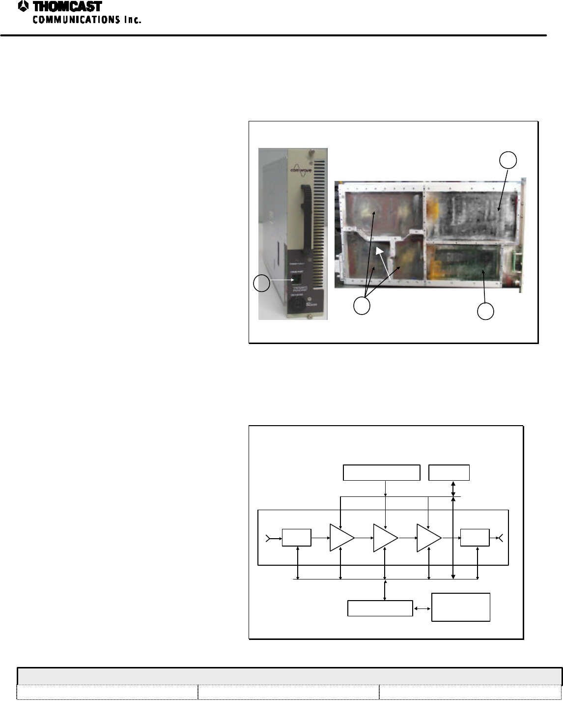
1
Power Amplifier Segment Theory of Operation - 04-294, 04-333
COMWAVE DIVISION
All information contained in this document is confidential and proprietary to THOMCAST and shall not be disclosed without the prior written permission of THOMCAST.
CREATED: KAS...................................................................9/15/98CHECKED: DMW................................................................9/18/98 RELEASED: PRC.................................................................10/20/98
Document #: DOC14-0008
REV: DEC.08.99
ECO #: 98-116
POWER AMPLIFIER SEGMENT THEORY OF OPERATION
The power amplifier segments of the high
power single channel transmitter series or
broadband booster series use the latest
technology in power FET’s. The transistors
provide high output power, as well as more
linearity and higher efficiency.
Mechanically, the power amplifier segments
have a plug-in architecture that allows hot
replacement. In addition to hot
replacement, the architecture of the
amplifier enables flexibility to tailor the
system to higher output power levels and
can be easily upgraded.
The power amplifier segment consists of a
microwave amplifier2, control board1, DC to
DC converter
3
, and a front panel. A
microcontroller system, located on the
control board, supervises and controls the
power amplifier segment in each of its
functions. The DC to DC converter reduces
48 V
DC
front-end power supply input to the
nominal amplifier voltage of 10.5 V. The
front panel displays the status of the
amplifier segment and interfaces the control
board to a computer by means of a serial
RS-232 port
4
. See Figure for numerical
references.
1
2
3
FRONT VIEW
SIDE VIEW
4
Figure 1: Power amplifier segment.
OPERATION
The amplifier segment is equipped with a
key lock switch on the front panel to retain
it in place. When pushing-in or pulling-out
the Segment, turn the key lock switch to the
OFF position. After plugging the amplifier
segment into the sub-rack and tightening
the front panel thumbscrews, turn the key-
lock switch to the ON position. The 10
V
DC
secondary power supply will start up
the control board, which applies a negative
voltage to the gates of the FET’s and turns
the DC to DC converter on. It also adjusts
the transistor’s current and releases the
input signal to the microwave amplifier.
The airflow passes through the heatsink
from the front to the rear of the sub-rack.
The airflow loss to the other power
amplifier segments during hot replacement
is negligible.
POWER AMPLIFIER SEGMENT BLOCK DIAGRAM
Microwave Amplifier
Rear Panel
Connector
DC to DC Converter
Control Panel
Front Panel
Connector & Key
Lock Switch
Document #: DOC15-0013 REV: C, ECO #: 98-116
Created by: KAS 9/15/98
Checked by: DMW 9/18/98
Released by: PRC 10/29/98
Figure 2 : DOC15-0013 power amplifier segment block diagram.

2
Power Amplifier Segment Theory of Operation - 04-294, 04-333
COMWAVE DIVISION
All information contained in this document is confidential and proprietary to THOMCAST and shall not be disclosed without the prior written permission of THOMCAST.
CREATED: KAS...................................................................9/15/98CHECKED: DMW................................................................9/18/98 RELEASED: PRC.................................................................10/20/98
Document #: DOC14-0008
REV: DEC.08.99
ECO #: 98-116
POWER AMPLIFIER SEGMENT SPECIFICATIONS
Table 1: DOC19-0014, REV D.
PARAMETER SPECIFICATION
Primary Voltage 48 VDC
Primary Current 4.9 A
Secondary Voltage 10 ±0.5 VDC
Secondary Current 400 mA
Communication Port RS-232 and RS-485
Input Power
Digital
Analog 12.0 dBm
17.5 dBm (@ POut1dB)
Output Power
Digital
Analog
41.5 dBm
47.0 dBm (@ POut1dB)
DC Connector Floating Molex p/n 15-06-0141
Impedance / RF Connector 50 O / Blindmate
Operating Temperature 0° to 50° C
Dimensions 10.3” H x 2.1” W x 17.1” D
26.16 cm H x 5.33 cm W x 43.43 cm D
Approximate Weight110 lbs (4 Kg)
• SPECIFICATIONS ARE SUBJECT TO CHANGE WITHOUT NOTICE.
1 Weight doesn’t include shipping material.
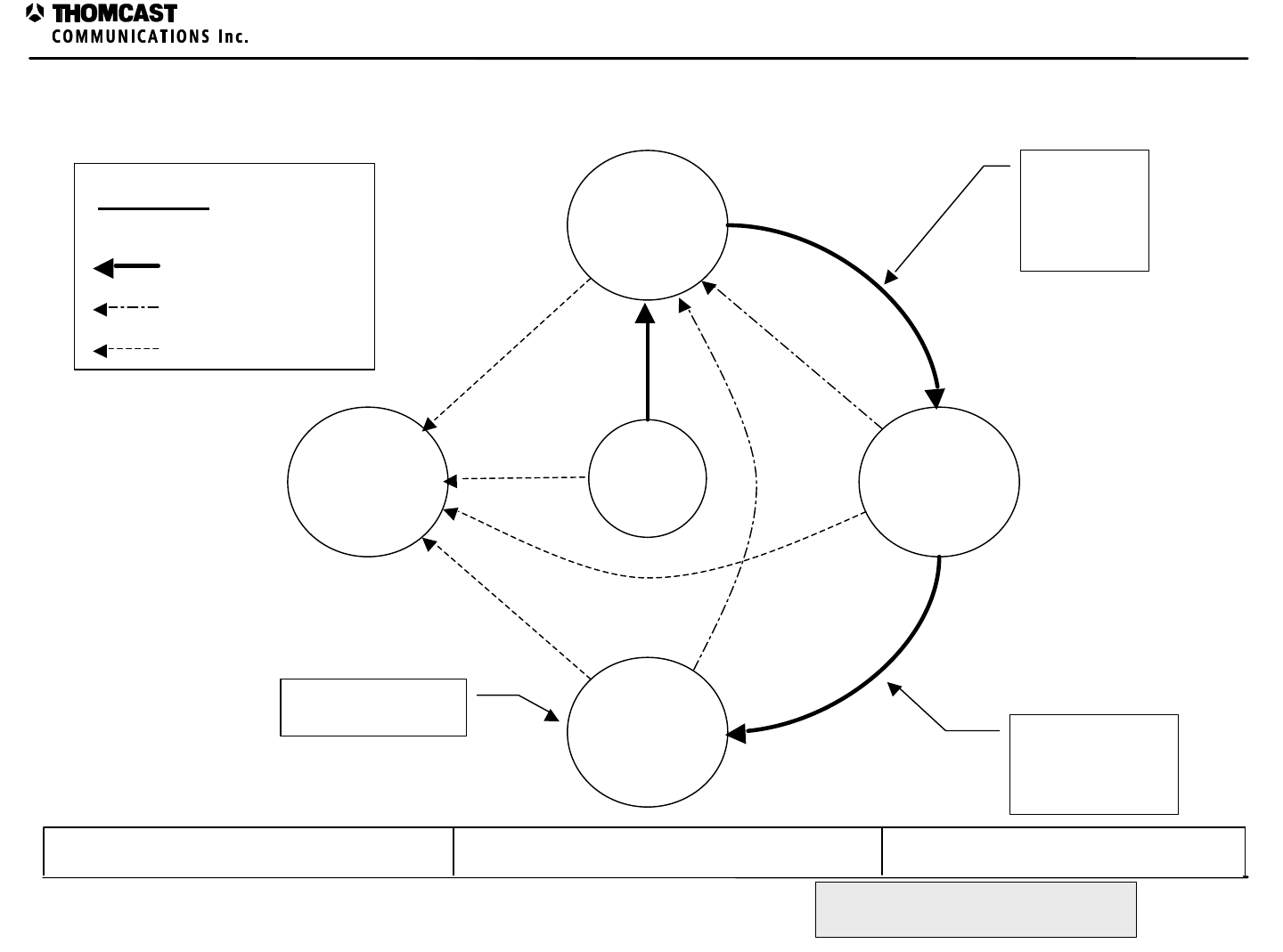
AMPLIFIER SEGMENT STATE FLOW DIAGRAM
Amplifier Segment State Flow Diagram
Document #: DOC21-0006
REV: A
Created by: Kimberly Simeone 11/23/98 Released by: Donald Wike 11/23/98Checked by: Christian Smith 11/23/98
All information contained in this document is confidential
and proprietary to COMWAVE and shall not be disclosed
without the prior written permission of COMWAVE.
RESET
COLD
STANDBY
FAILED
0
TRANSMIT
RAMP
UP
Front panel
switch on
driver placed
out of
standby
Completion of
ramp up delay
loop. Transistors
at nominal current.
Established AGC at
nominal power
Normal State Progression
Standby control active
Module failure
Arrow Key
COMWAVE DIVISION
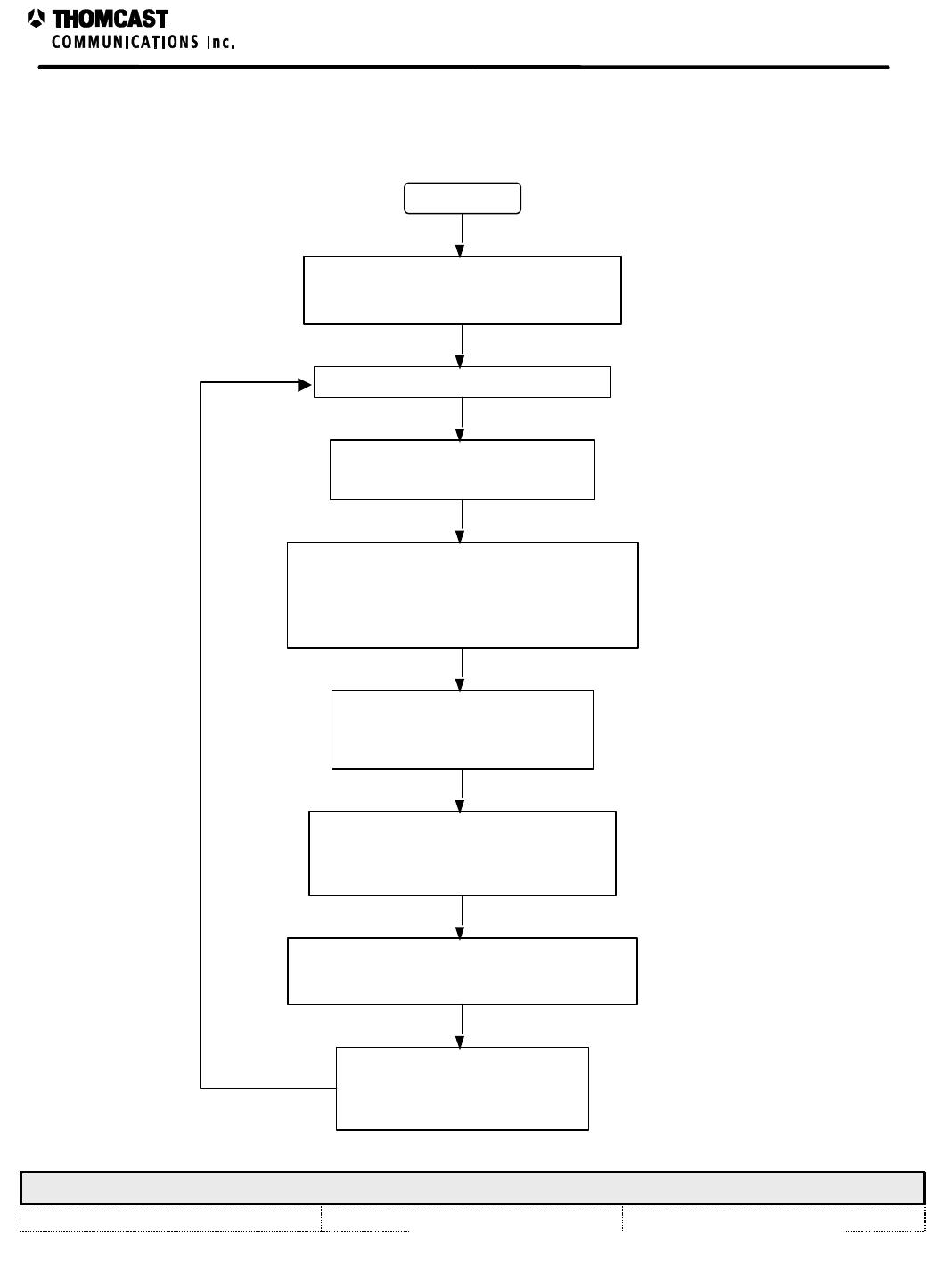
COMWAVE DIVISION
All information contained in this document is confidential and proprietary to THOMCAST and shall not be disclosed without the prior written permission of THOMCAST.
CREATED: KAS 11/20/98 CHECKED: CTS 11/23/98 RELEASED: DMW 11/23/98
Document #: DOC21-0005 REV: DEC.08.99 1
FIRMWARE FLOWCHART
START
Initialize module, network and
operational mode
Begin main loop
Update the operational
parameters of the module
Test the operational parameters
against programmed limits to ensure
valid operation of the module
Determine the operational
state of the module
Record invalid operational
parameters into EEPROM for
later analysis
Control gate and ALC functions of
the module based on current state.
Check for and
communicate over the
RS-485 network
Firmware Flowchart Power Amplifier Segment
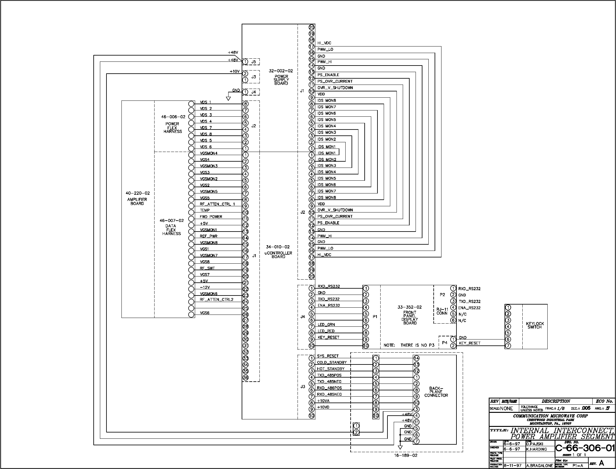
SECTION 5
PREVIOUS
Print
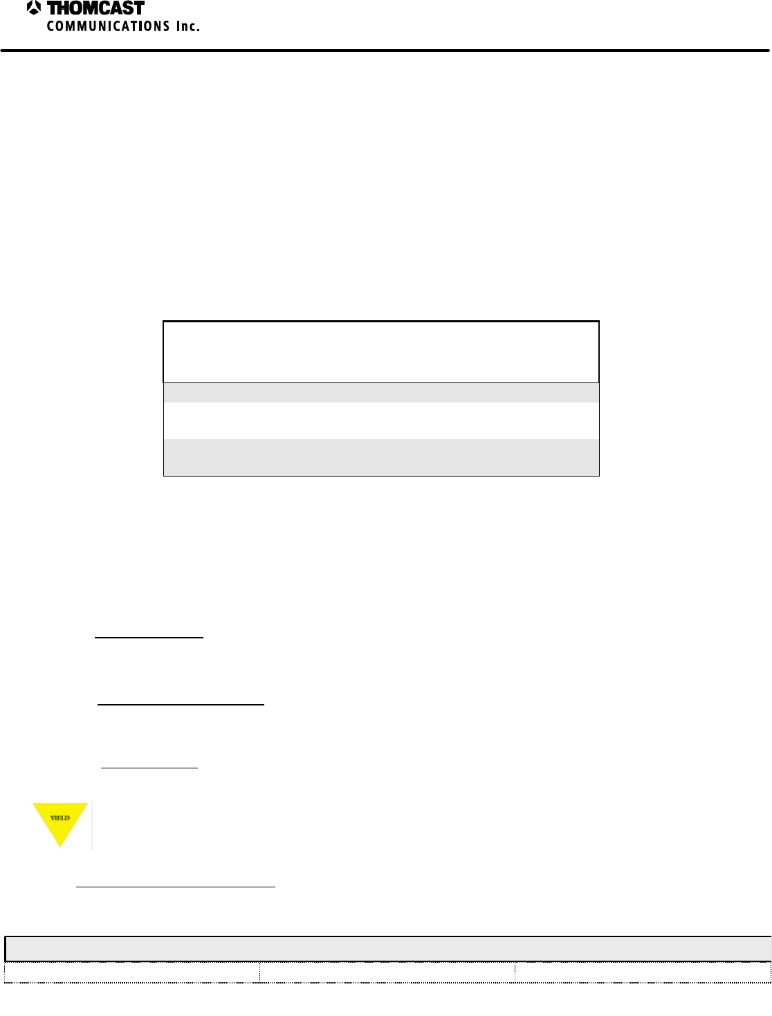
1
Customer Service
COMWAVE DIVISION
All information contained in this document is confidential and proprietary to THOMCAST and shall not be disclosed without the prior written permission of THOMCAST.
CREATED: KAS ............5/6/99 ECO #: 99-035, 3/25/99 CHECKED: DMW..............................................................1/18/99 RELEASED: PRC .............................................................. 1/18/99
Document #: DOC20-0001
REV: FEB.09.00
CUSTOMER SERVICE
CONTACT INFORMATION
DURING BUSINESS HOURS
Inquiries may be directed to Thomcast Communications, Comwave Division during business hours, 8 am to 5
pm Monday through Friday. When the automated attendant answers you will be given the option of dialing
your party direct or speaking with the operator.
AFTER BUSINESS HOURS
If you need emergency assistance due to equipment shutdown or malfunction, customer support personnel are
available 24 hours a day. Call Comwave at one of the numbers listed below; when the automated attendant
answers press 6, leave your name, company name, phone number, equipment model number(s), and a brief
description of the problem you’re encountering. When you hang up the system will automatically page the on-
call technician who will then return your call in a timely manner. You can listen to the message prompt for
other options as well, however, for emergency assistance you MUST use option 6.
Thomcast Communications, Comwave Division
Crestwood Industrial Park, 395 Oakhill Road
Mountaintop, PA 18707
1-800-266-9283 USA & Canada
1-570-474-6751 International1 & USA
(Please note, as of 12/98, our area code changed from 717 to 570)
1-570-474-5469 FAX
(Please note, as of 12/98, our area code changed from 717 to 570)
COMMENTS/SUGGESTIONS
Please forward comments regarding documentation content and/or layout, or suggestions to improve Comwave
publications to ksimeone@thomcastcom.com.
EQUIPMENT RETURNS
If the equipment requires return for factory service, please follow the guidelines listed. Thomcast cannot be
held responsible for damaged equipment received due to improper packing; contact Thomcast with any
questions or concerns.
1. Contact Comwave: Call Comwave to report the problem and to obtain a “Return Authorization”
number2 (RA). This enables accurate tracking and identity of returned equipment for prompt and efficient
service.
2. Obtain packaging materials: Use original boxes and packing materials when returning any equipment.
This will safeguard against most in-transit damages. If original boxes and packing materials are not available,
contact Thomcast to obtain replacement materials prior to shipping, they are provided at a nominal cost.
3. Pack equipment: Use original packing materials and directions provided. Most equipment is packed in a
box within another box; this varies with each product. Double boxing provides maximum protection.
Caution: Do not pack equipment using “PEANUTS” as filler it does NOT provide sufficient protection
during shipping. Rough handling by the carrier may cause permanent damage to the equipment.
Thomcast cannot be held responsible for damaged equipment received due to improper packing.
1 International calls must dial the country code before the phone number, i.e. 001-570-474-6751.
2 If you do not obtain an RA number prior to returning equipment Thomcast cannot be held responsible for delays in repair and return
time.
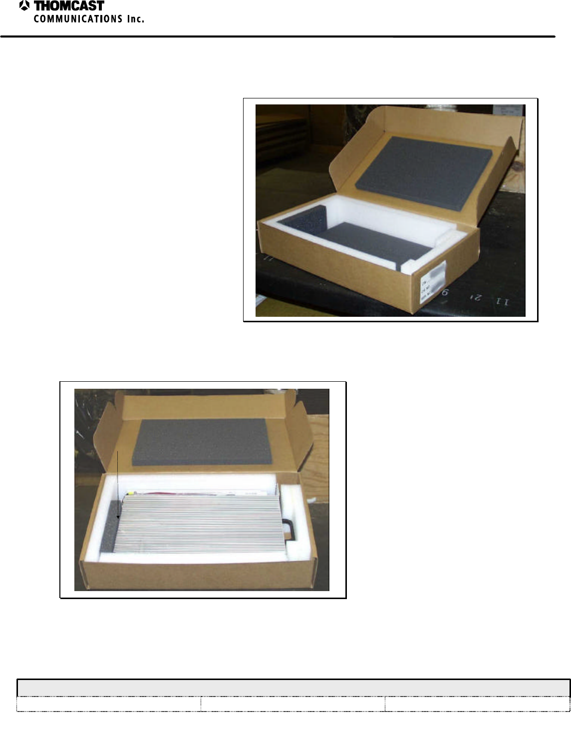
1
Return Packaging of the Power Amplifier Segment
COMWAVE DIVISION
All information contained in this document is confidential and proprietary to THOMCAST and shall not be disclosed without the prior written permission of THOMCAST.
CREATED: KAS ................................................................10/21/98 CHECKED: SB..................................................................10/22/98
RELEASED: DMW
........................................................... 10/22/98
Document #: DOC20-0003
REV: DEC.06.99
ECO #: 98-116
RETURN PACKAGING OF THE POWER AMPLIFER SEGMENT
1. Start with an empty power amplifier
segment box, shown in Figure 1. If
you don’t have one please inform
Comwave customer service when you
contact them for a return authorization
(RA) number, which you MUST do
prior to returning ANY equipment.
2. Place the power amplifier segment into
the box, as shown in Figure 2. The
heatsink should always face up and the
connectors on the rear of the power
amp segment rest against the soft gray
foam for protection.
Figure 1: Empty power amplifier segment box.
HEATSINK
REAR
Figure 2: Boxed power amplifier segment.
3. Fold the edges of the inner box in and
close.
4. Place the inner box into the 4-pack
master (outer box), being sure to
include three empty power amplifier
boxes for a secure fit, as shown in
Figure 3. The power amplifier
segments are generally packed 4 per
master box and shipped. When
returning segment(s) please pack them
the same way, ALL boxes will be
returned to you. If you need to
assemble a master box, use 2” clear
box tape over the bottom seam, using
three layers to assure strength. Then
put 4 pieces of fiberglass strapping
tape over the edges.
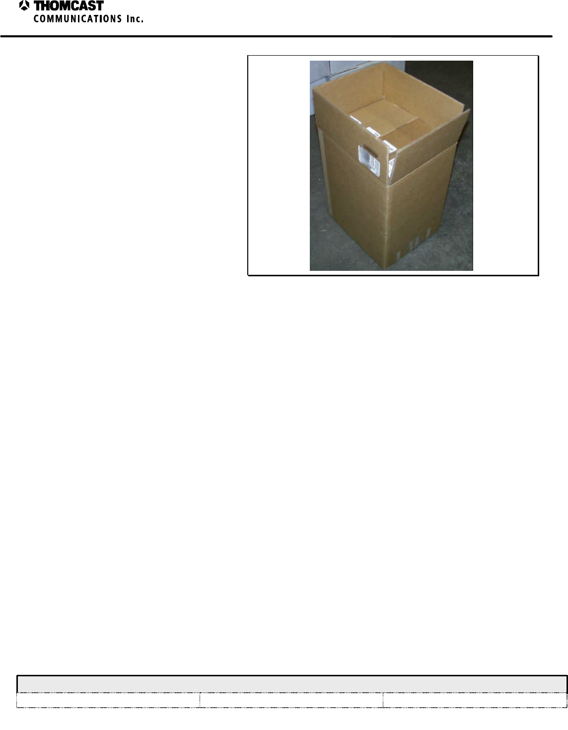
2
Return Packaging of the Power Amplifier Segment
COMWAVE DIVISION
All information contained in this document is confidential and proprietary to THOMCAST and shall not be disclosed without the prior written permission of THOMCAST.
CREATED: KAS ................................................................10/21/98 CHECKED: SB..................................................................10/22/98
RELEASED: DMW
........................................................... 10/22/98
Document #: DOC20-0003
REV: DEC.06.99
ECO #: 98-116
5. Close the 4-pack master box and seal
the top seam with 2” clear box tape,
using three layers to assure strength.
Then put 4 pieces of fiberglass
strapping tape over the edges. Clearly
mark the RA number on the outside of
the box before shipping.
Figure 3: Power amplifier segments ready to ship.