Thomson Broadcast and Multimedia 8BUSDA5000C 50 Watt Frequency Agile Digital Transmitter System User Manual 10 0046 SD5000C
Thomson Broadcast & Multimedia, Inc. 50 Watt Frequency Agile Digital Transmitter System 10 0046 SD5000C
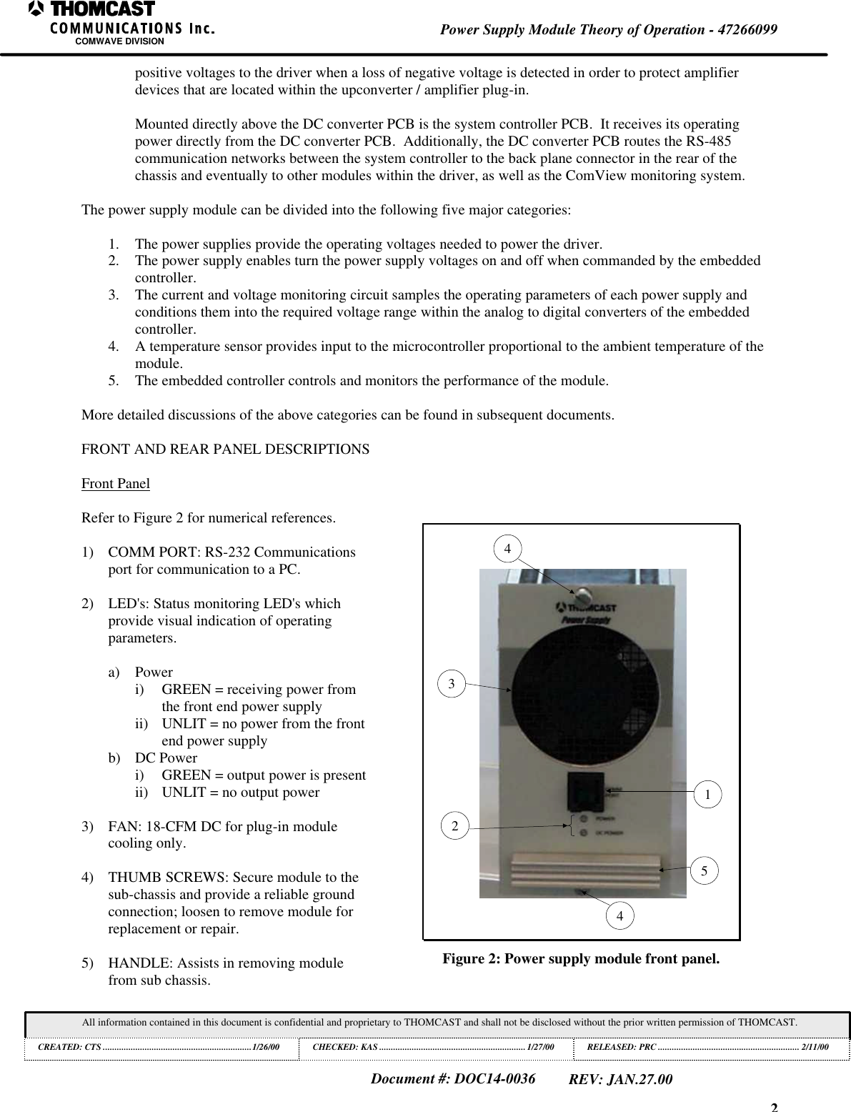
Contents
- 1. SDA5000C transmitter
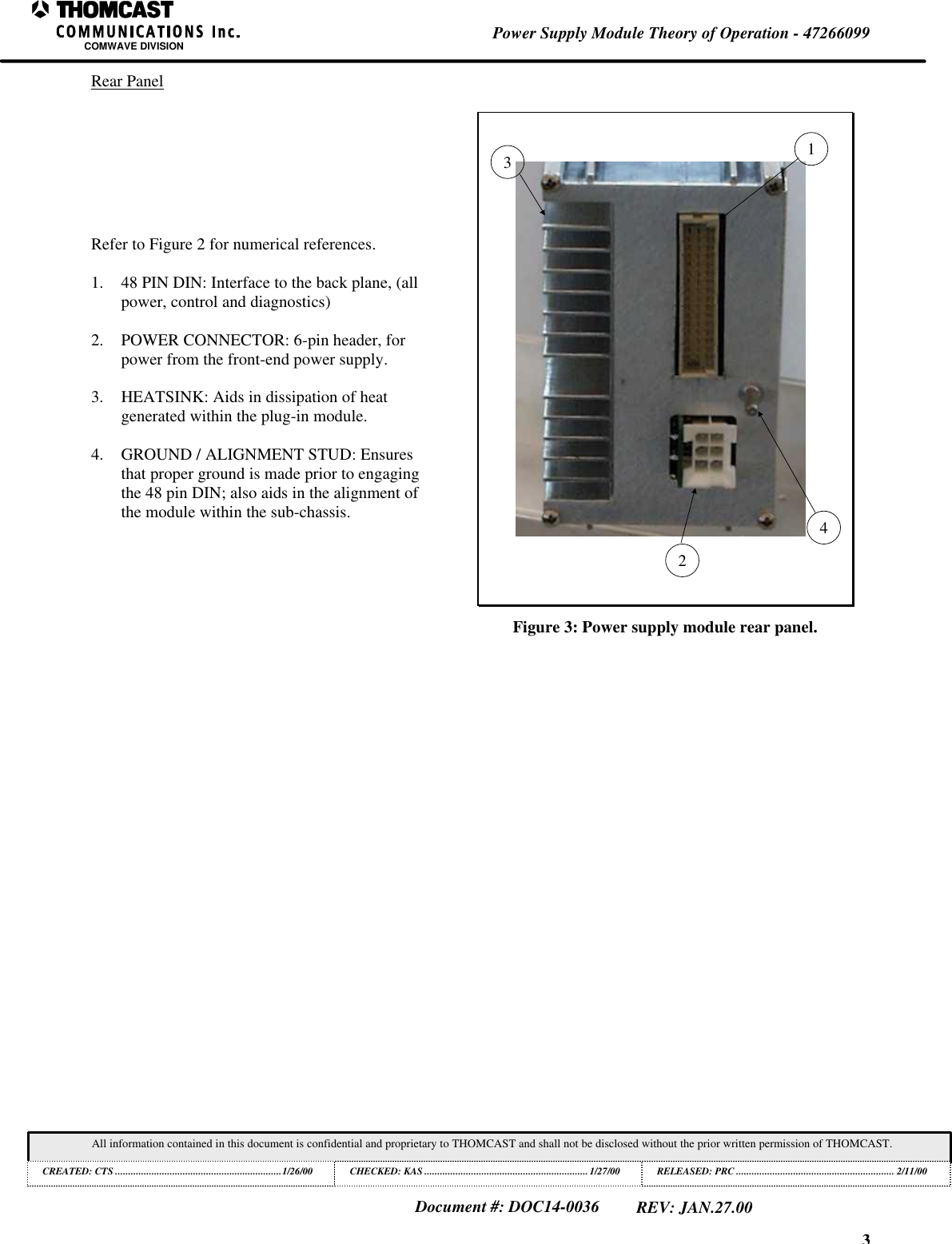
- 2. Agile synthesizer drawer
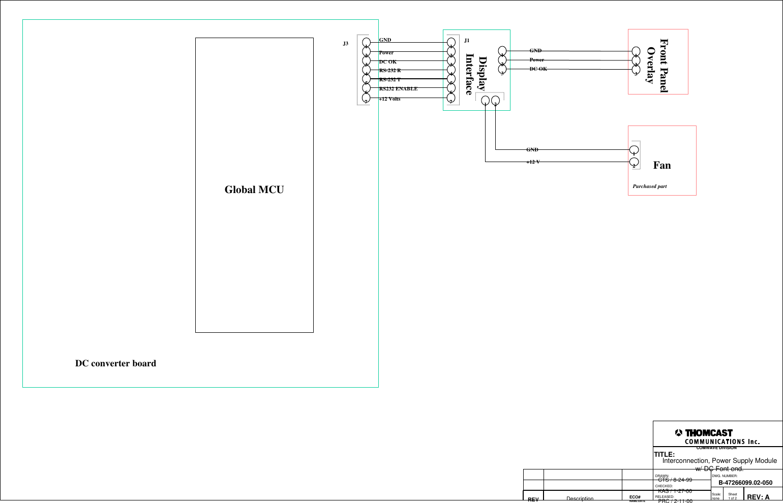
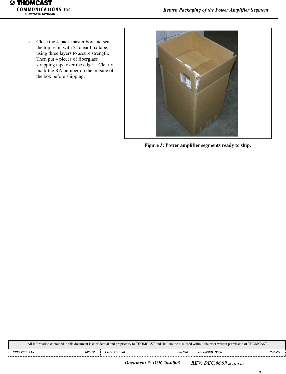
SDA5000C transmitter

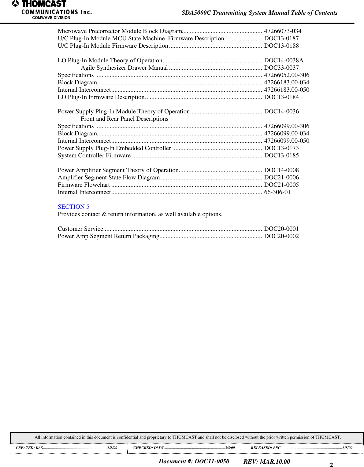
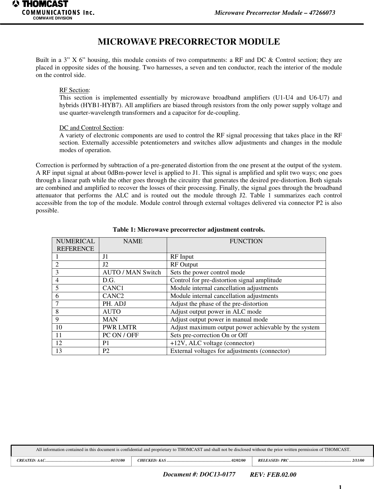
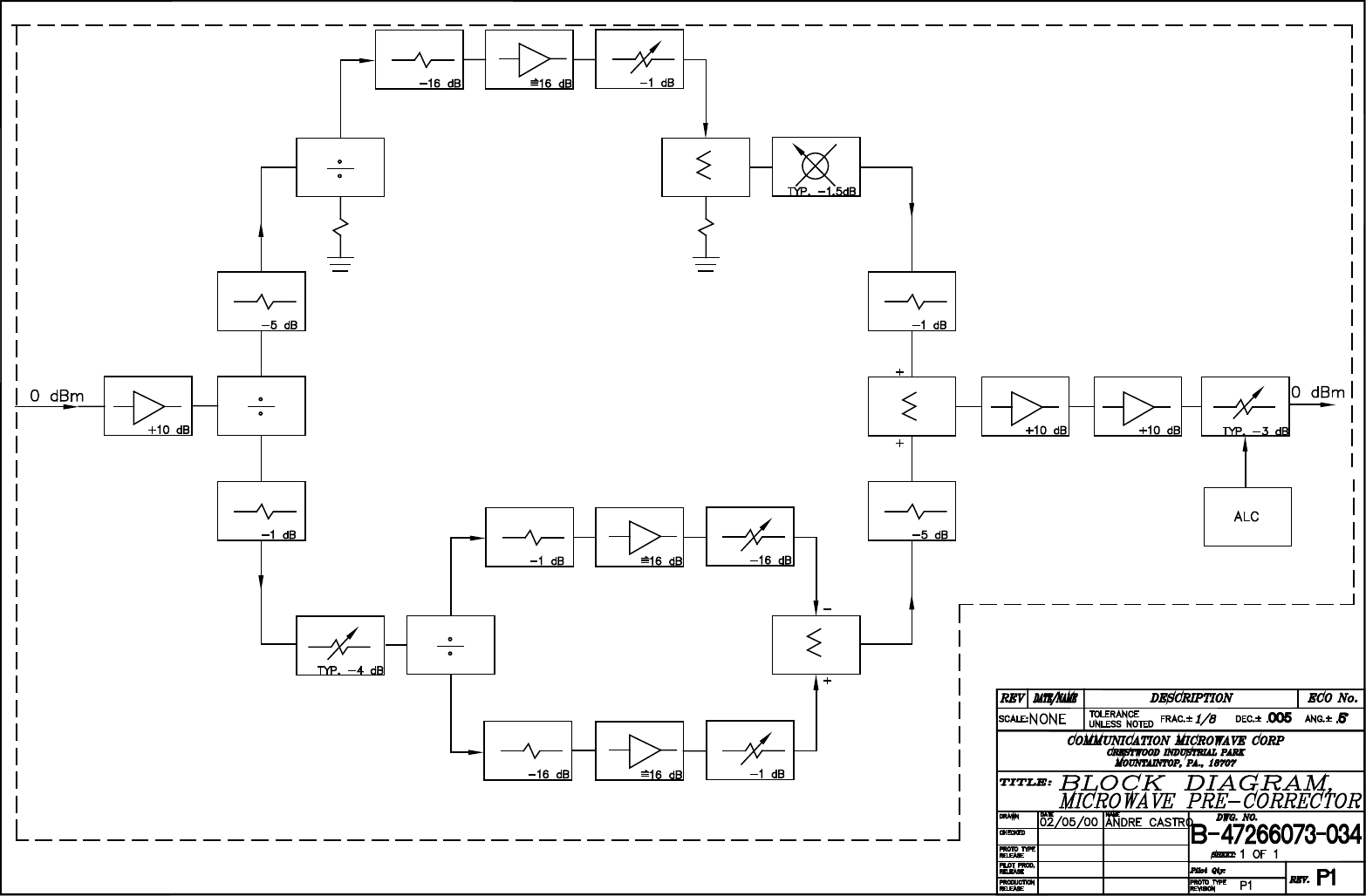
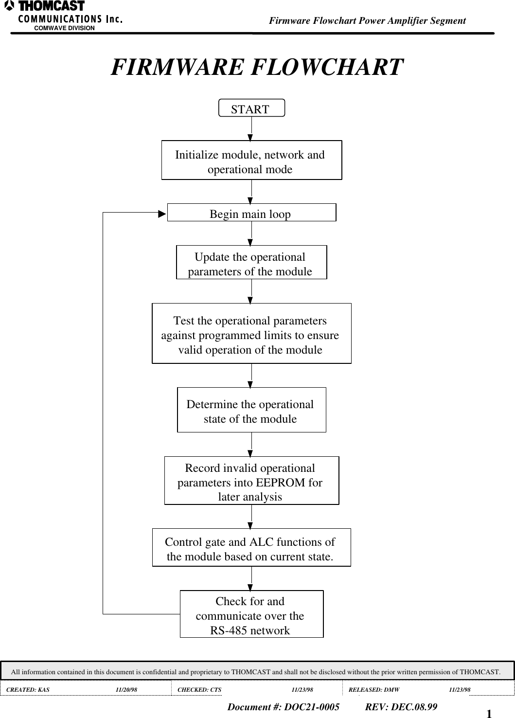
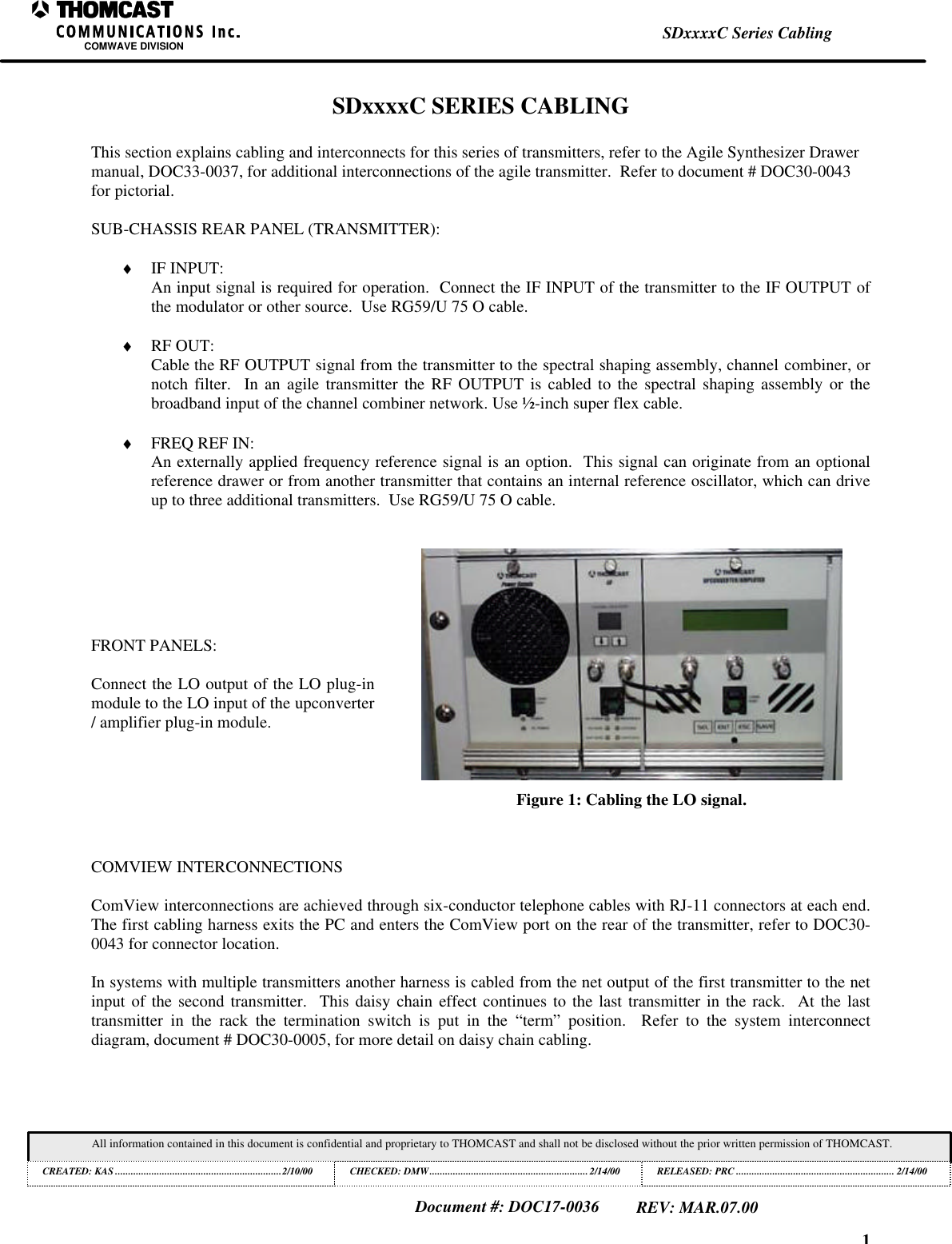
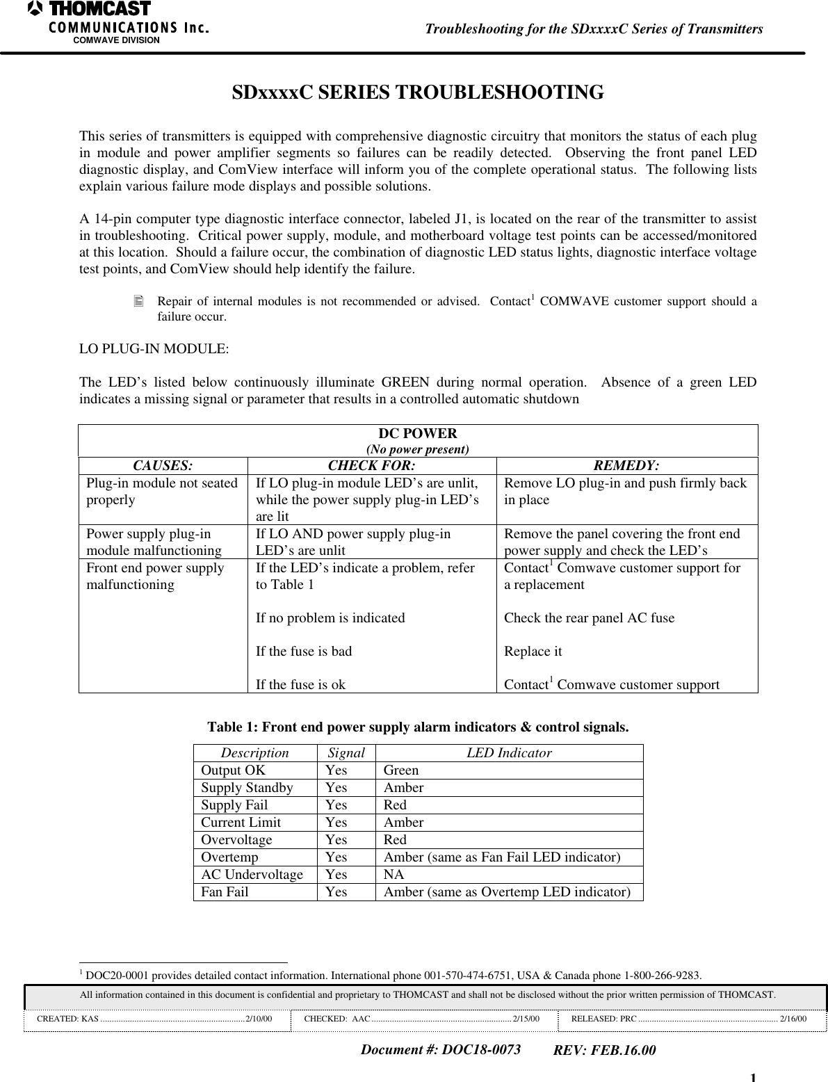
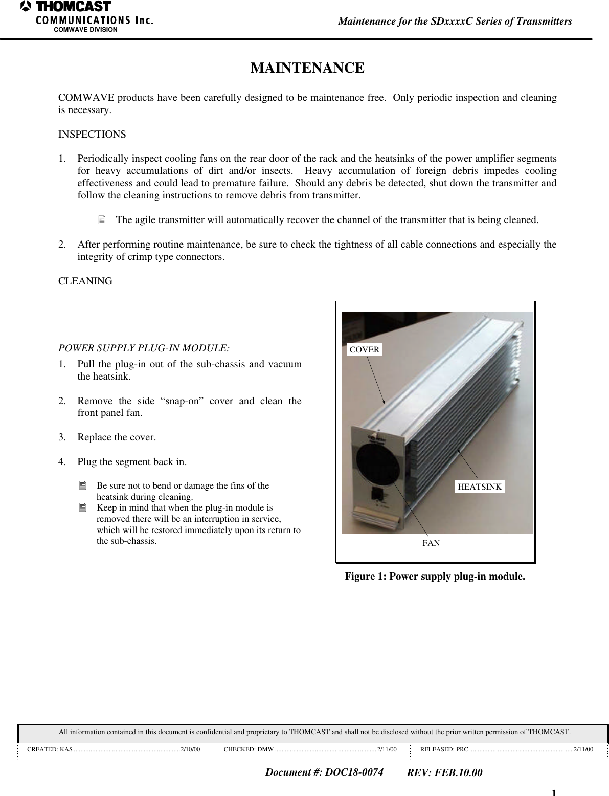
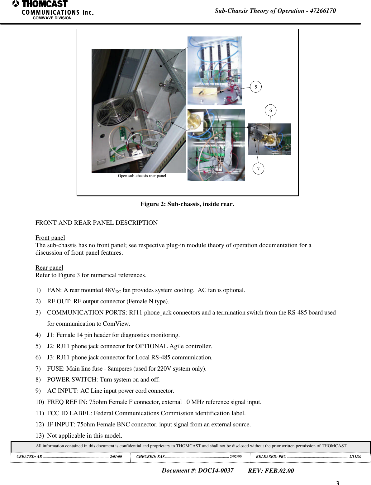
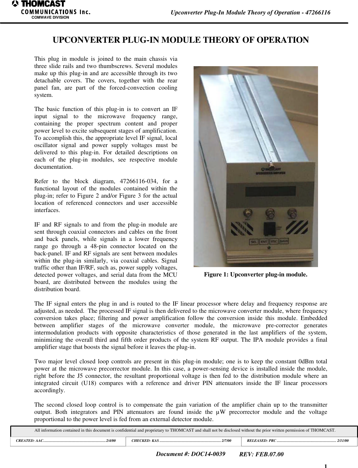
![2SDxxxxC Transmitter Series Top Level DescriptionCOMWAVE DIVISIONAll information contained in this document is confidential and proprietary to THOMCAST and shall not be disclosed without the prior written permission of THOMCAST.CREATED: KAS ................................................................1/30/00 CHECKED: PRC............................................................... 1/31/00RELEASED: PRC............................................................. 2/10/00Document #: DOC13-0178REV: MAR.07.00SPLITTERPOWERAMPLIFIERSEGMENTS[1 TO 4]COMBINERLOUPCONVERTERMODULEOUTPUTCOUPLERFigure 1: System RF signal path.SPLITTERPOWERAMPLIFIERSEGMENTS[1 TO 4]UPCONVERTERMODULECOMBINERAGILE SYNTHESIZER DRAWERIF to UHFUPCONVERTERMODULEOUTPUTCOUPLERFigure 2: Agile system RF signal path.](https://usermanual.wiki/Thomson-Broadcast-and-Multimedia/8BUSDA5000C.SDA5000C-transmitter/User-Guide-90827-Page-7.png)
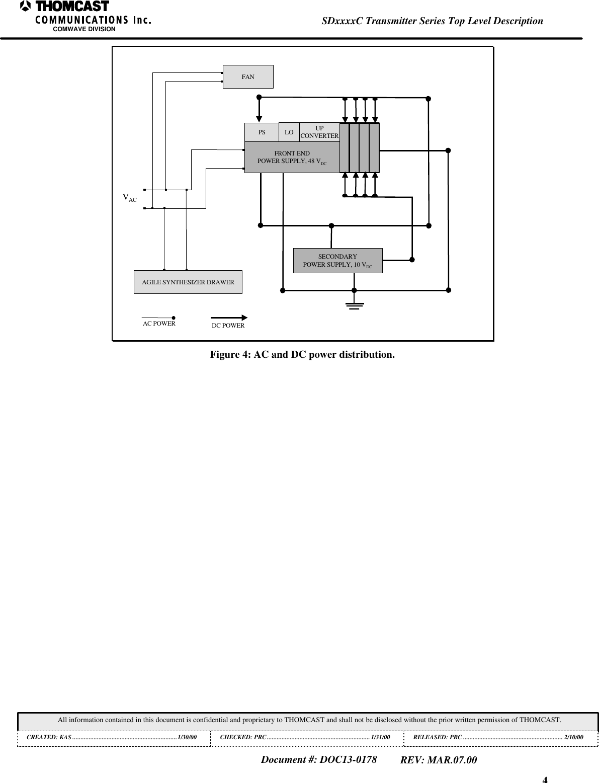
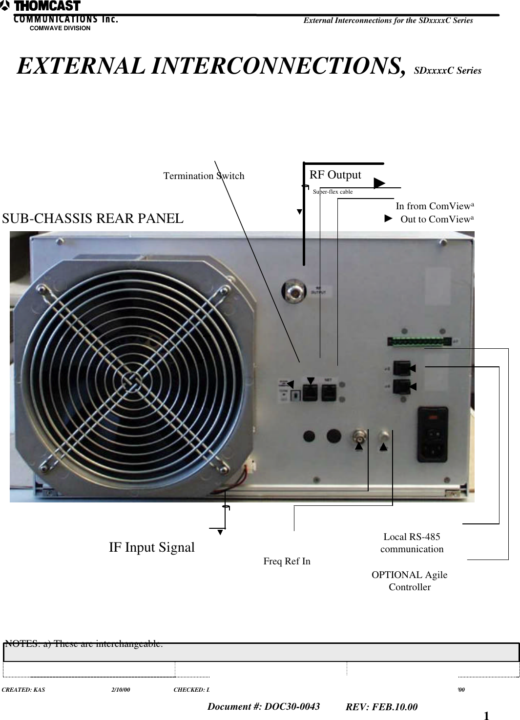
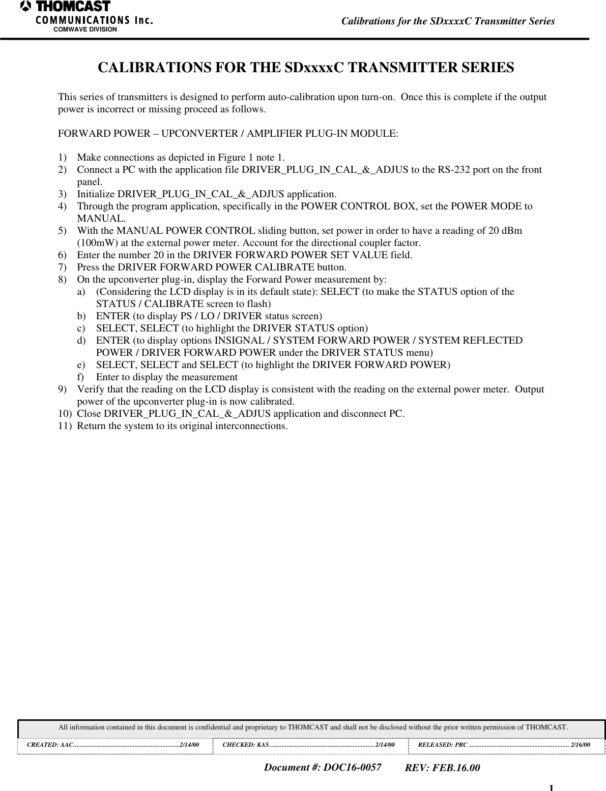
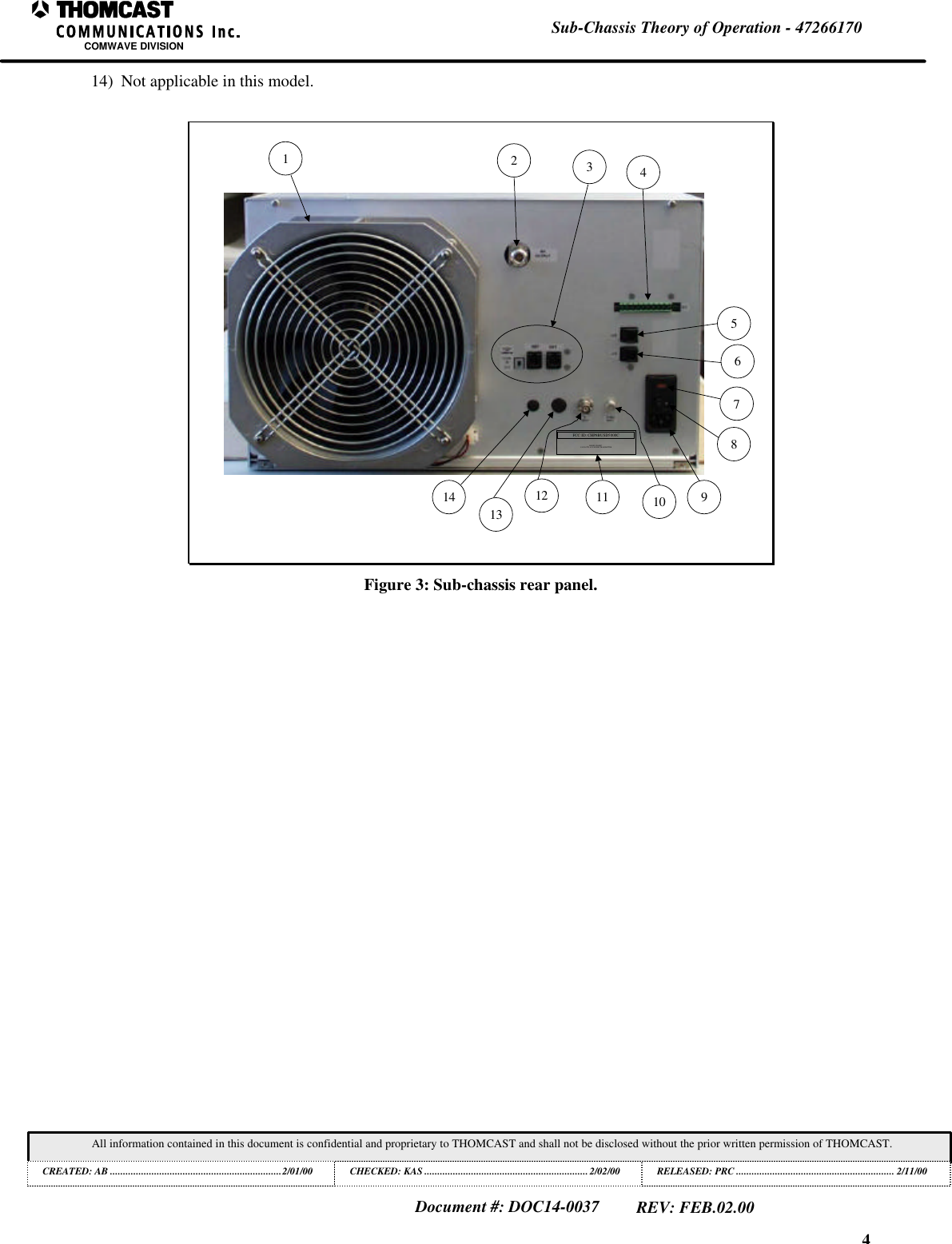
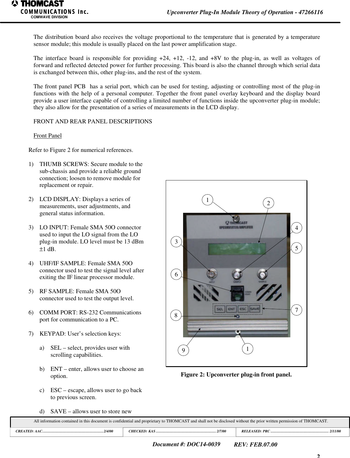

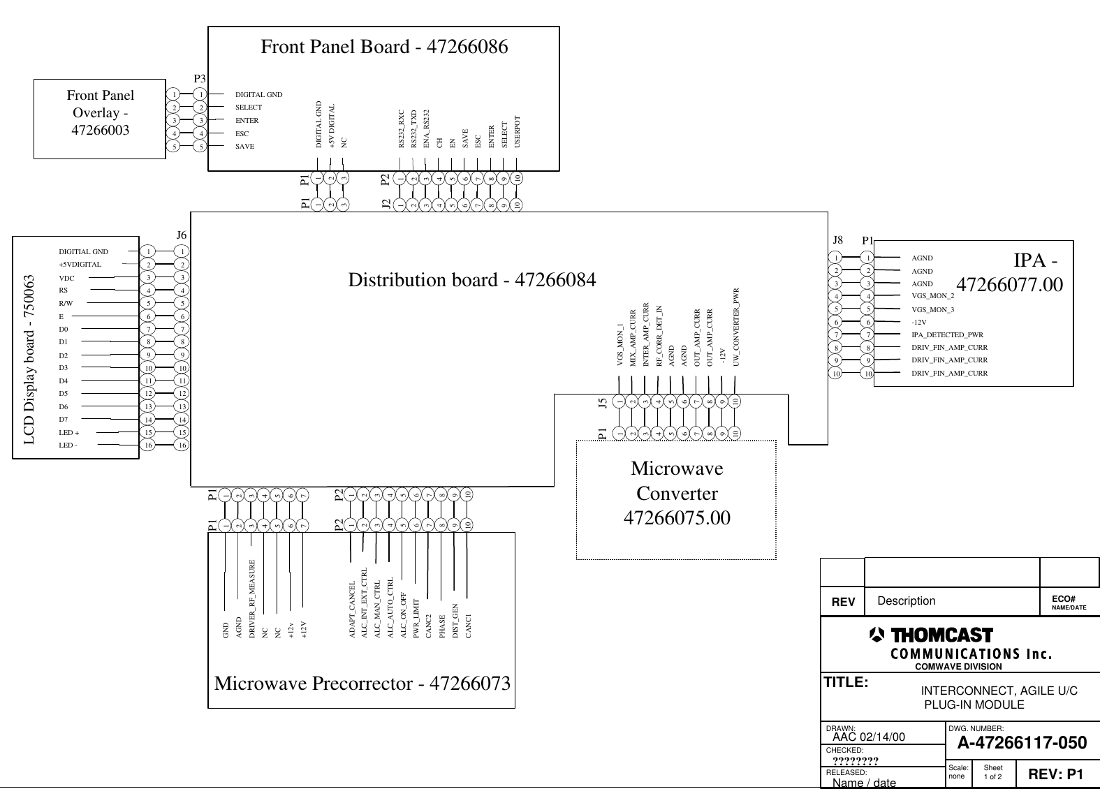
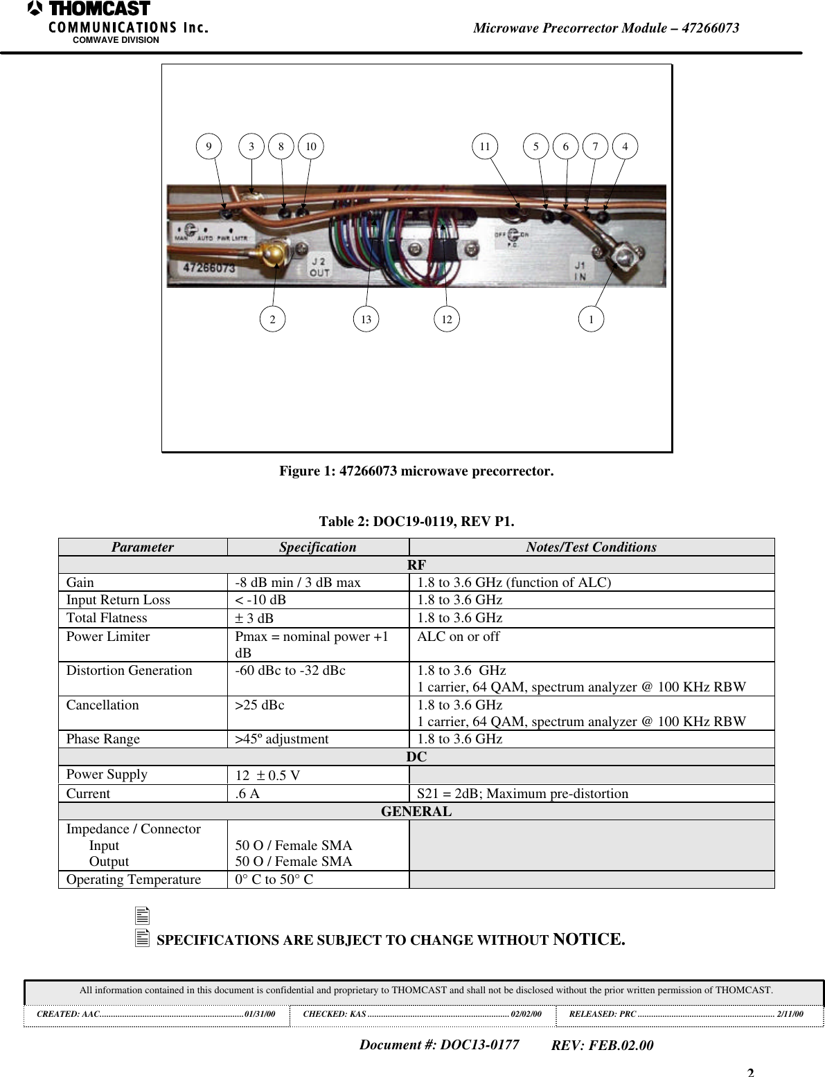
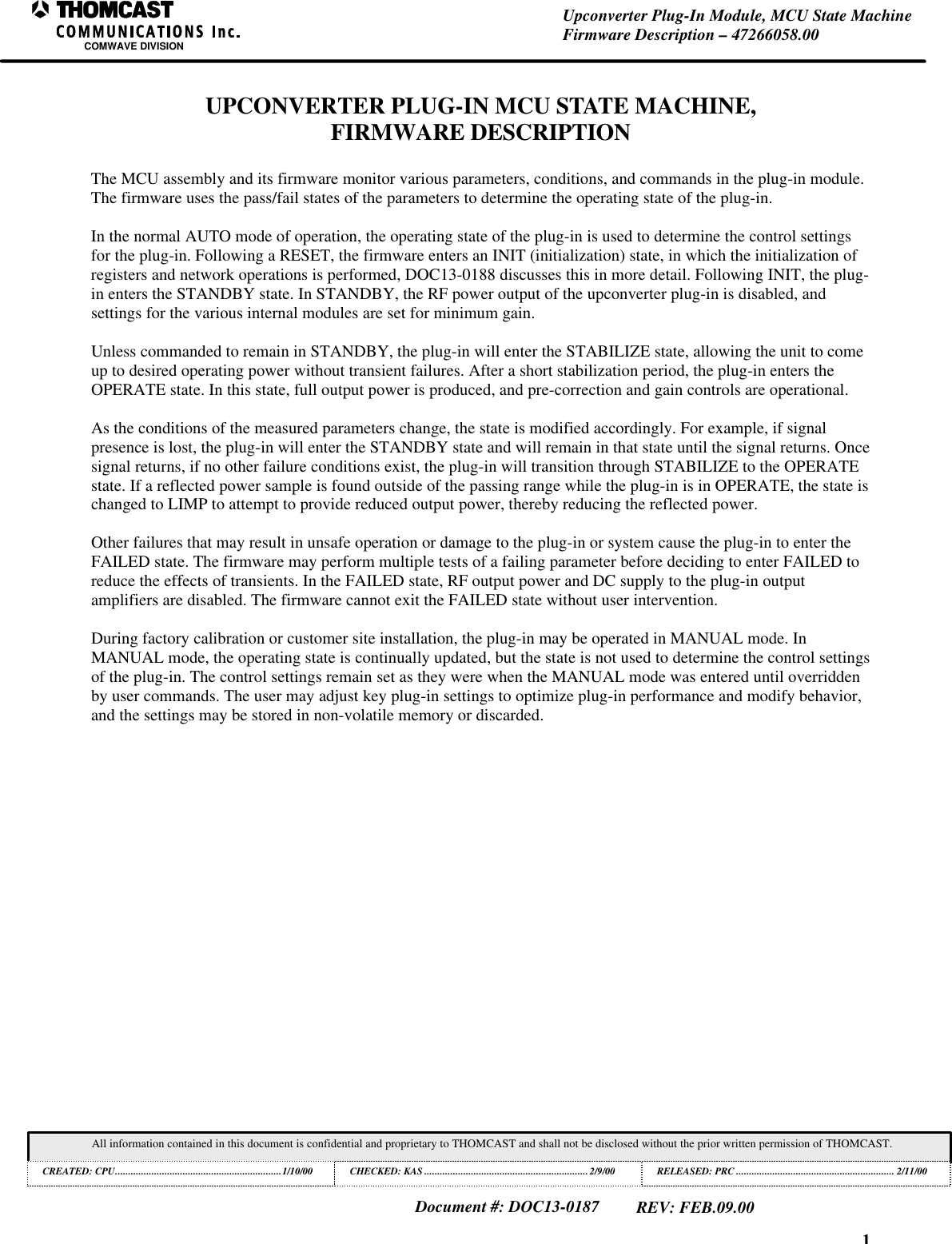
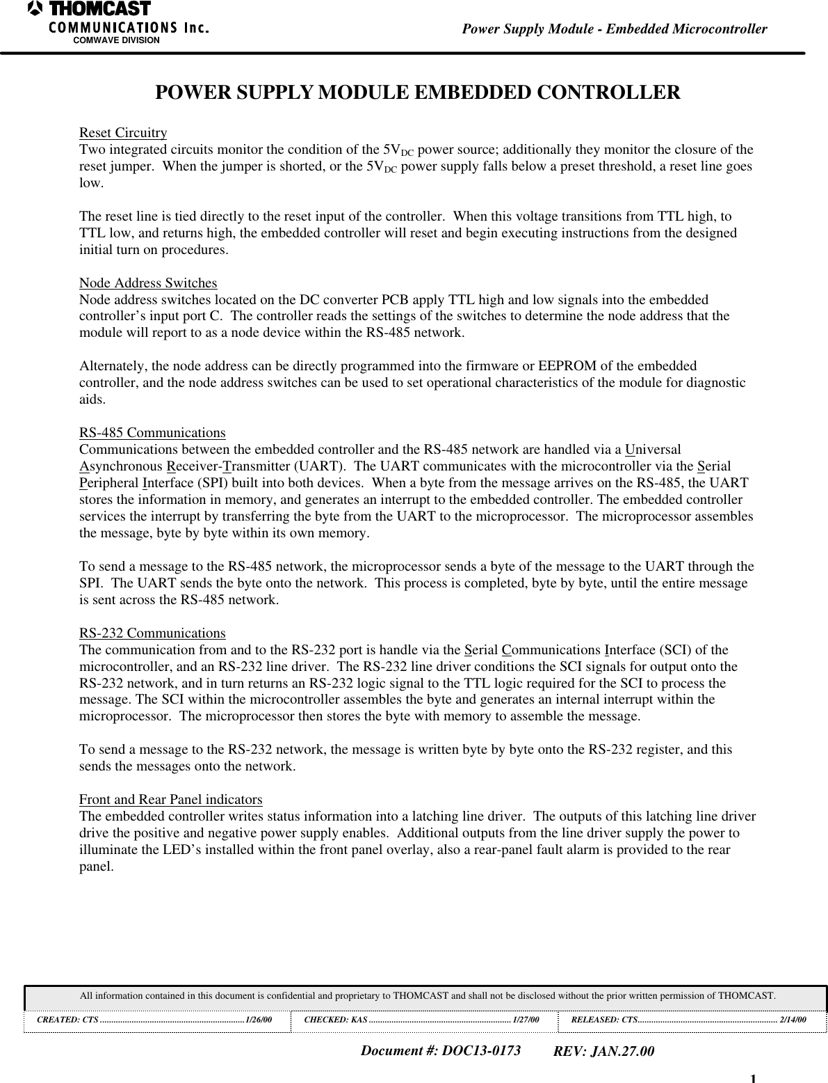
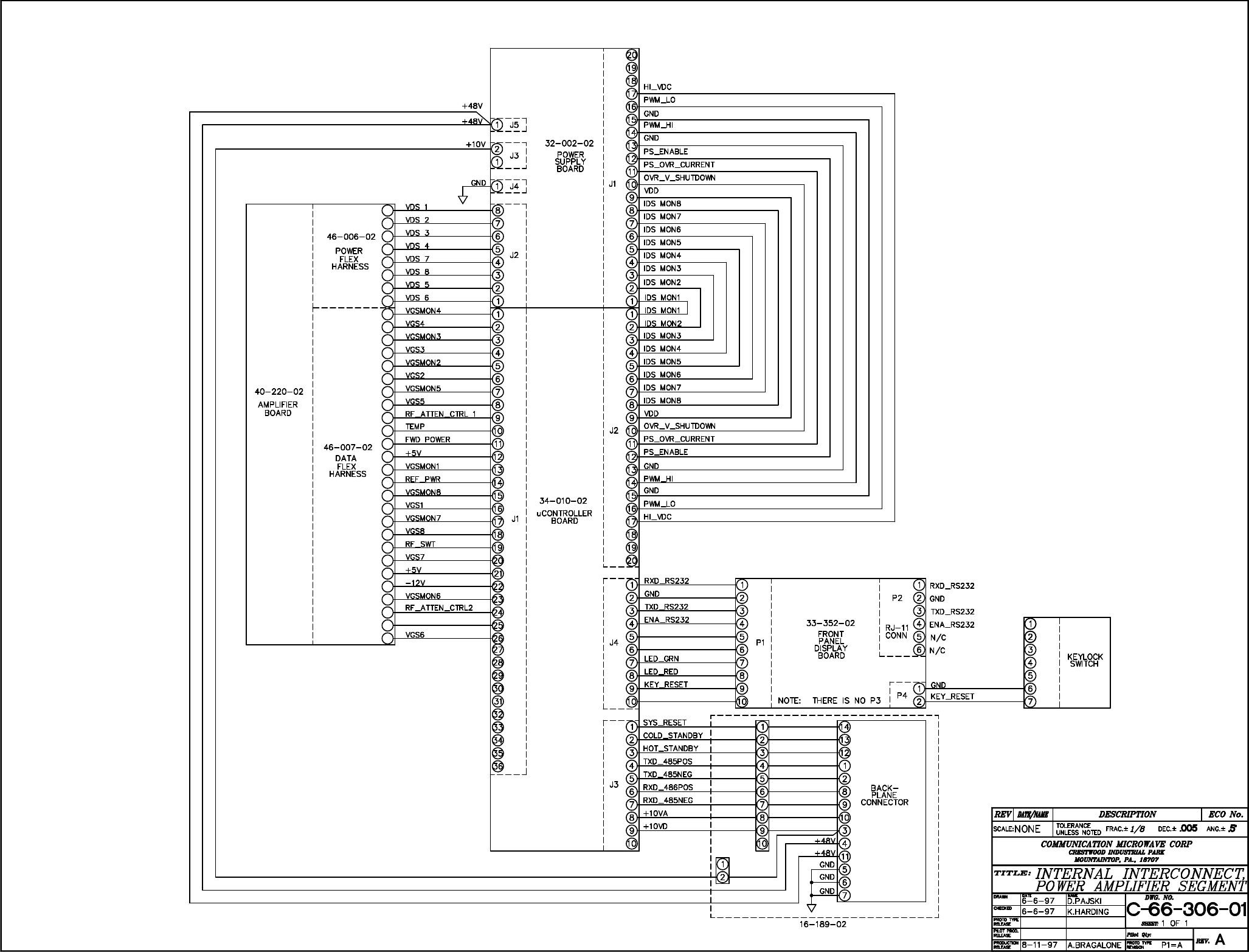
![Distribution board - 47266084ENCODER_GAIN_CTL+12VNCGNDRS485_LOCAL_T-FWDPWR_1REMOTE_SHDNGNDBOOSTER_INSIGNAL+8V+12V+24VRS485_LOCAL_R-RS485_LOCAL_T+RFLTDPWR_1+8V+12VIF Linear Processor -47266082.00AGNDAGNDIF_THRESHOLDIF_ATTNCFREQ_RESP#2+12VAAUX_ATT_2FREQ_RESP#1+12VADRAWN:RELEASED:CHECKED:DWG. NUMBER:TITLE:REV: P1A-47266117-050AAC 02/14/00Name / date???????? Scale:none Sheet2 of 2COMWAVE DIVISIONREV Description ECO#NAME/DATEGND+5VATEMPERATURE123123Temperature Sensor- 4726620312Fan1234567891012345678910J4P112345678910111213141516171819202122232425261234567891011121314151617181920212223242526J2J1IN_SIGNAL-12VRS485_LOCAL_R+GNDGNDAGC_LEVELDRIVER_FAULTNCNC1234513141617181920212229323334353641444548GNDInterface Board - 47266149J1DRIV_FIN_AMP_CURR [3,4]1234567891011121314151617181920GNDSYS_FWD_DET_PWR [4]SYS_RFL_DET_PWR [2,4]USER_POT [5]ADAPT_CORR [5]VDD_IO [3]OUT_AMP_CURR [3,4]DRIVER_RF_MEAS [4]+8v [3.5]MIX_AMP_CURR [3,4]INTER_AMP_CURR [3,4]AGC_LEVEL [4,5]ADAPT_CANCEL [4]TEMP [3]VGS_MON_1 [4]VGS_MON_2 [4]VGS_MON_3 [4]8VSW [3]1234567891011121314151617181920DAC_2_CS [1]1234567891011121314151617181920GNDDO [5]D1 [5]D2 [5]D3 [5]DAC_1_CS [1]D7 [5]DAC_3_CS [1]D4 [5]D5 [5]D6 [5]AGC_ON_OFF [2]ALC_ON_OFF [2]AGC_INT_EXT_CTRL [2]ALC_INT_EXT_CTRL [2]EN [5]RS [5]R/W [5]1234567891011121314151617181920 E [5]J102J103Microcontroller Board - 47266058.00DRIVER_FAULT [5]1234567891011121314151617181920GNDENTER [5]ESC [5]CH [5]ENA_RS232 [5]ENCODER_GAIN_CTRL [5]REMOTE_SHDN [5]SAVE [5]SELECT [5]IN_SIGNAL [4,5]FST_RLCTD_SHTD [2]SS [1]LC_DAC [1]MOSI [1]CLOCK [1]SUPPLIES_EN [3]1234567891011121314151617181920 ALC_LOOP_SELECT_2 [2,4]J1011234567891011121314151617181920GNDRS485_LOCAL_R- [5]RS485_LOCAL_T+ [5]RS485_LOCAL_T- [5]RS485_LOCAL_R+ [5]RS232_TXD [5]RS232_RXD [5]-12V [3,4,5]+12VA [2,3,4,5]1234567891011121314151617181920 +12VA [2,3,4,5]J100Microcontroller Board - 47266058.00INTERCONNECT, AGILE U/C PLUG-IN MODULE](https://usermanual.wiki/Thomson-Broadcast-and-Multimedia/8BUSDA5000C.SDA5000C-transmitter/User-Guide-90827-Page-46.png)