Toshiba Mk1032Gax Users Manual
MK1032GAX MK-1032GAX
2014-12-13
: Toshiba Toshiba-Mk1032Gax-Users-Manual-128427 toshiba-mk1032gax-users-manual-128427 toshiba pdf
Open the PDF directly: View PDF ![]() .
.
Page Count: 159 [warning: Documents this large are best viewed by clicking the View PDF Link!]

Toshiba Corporation Digital Media Network Company
Page 1 of 159
© 2004, Copyright TOSHIBA Corporation All Rights Reserved
1.1.1.1.1.1.1.1 TOSHIBA
TOSHIBA
Hard Disk Drive Specification
2.5 inch Hard Disk Drive
MK1032GAX
Rev. 00
REF
360051242

Toshiba Corporation Digital Media Network Company
Page 2 of 159
© 2004, Copyright TOSHIBA Corporation All Rights Reserved
Revision History
2.5 inch Hard Disk Drive MK1032GAX Product Specification
Revision Date
00 2004-09-28 Initial issue
Toshiba Corporation Digital Media Network Company
Page 3 of 159
© 2004, Copyright TOSHIBA Corporation All Rights Reserved
The hard disk drive and product specifications contain essential information for the protection of
users and others from possible injury and property damage and to ensure correct handling.
Please check that you fully understand the definition of the following messages (signs and
graphical symbols) before going on to read the text, and always follow the instructions.
Please describe requirements in the instruction manual of the product in which the drive is
mounted and ensure that users are made thoroughly aware of them.
IMPORTANT MESSAGES
Read this manual and follow its instructions. Signal words such as CAUTION and NOTE,
will be followed by important safety information that must be carefully reviewed.
Indicates a potentially hazardous situation which if not avoided, may result
in minor injury or property damage.
NOTE Gives you helpful information.
・Toshiba Corporation shall not be liable for any damage due to the fault or negligence
of users, fire, earthquake, or other accident beyond the control of Toshiba
Corporation.
・Toshiba Corporation shall not be liable for any incidental or consequential damages
including but not limited to change or loss of stored data, loss of profit, or
interruption of business, which are caused by use or non-usability of the product.
・Toshiba Corporation shall not be liable for any damage result from failure to comply
with the contents in the product specification.
・Toshiba Corporation shall not be liable for any damage based on use of the product
in combination with connection devices, software, or other devices provided by
Toshiba Corporation with the product.
SAFETY
LIMITATION OF LIABILITY

Toshiba Corporation Digital Media Network Company
Page 4 of 159
© 2004, Copyright TOSHIBA Corporation All Rights Reserved
● Since the drive is not designed or manufactured to be used for a system including
equipment (*1) directly linked with human life, etc., Toshiba Corporation shall not
be liable for this type of use.
*1: Equipment directly linked with human life, etc. corresponds to the
following.
−Medical equipment such as life support systems, equipment used in
operations,etc.
● When the drive is to be used for a system including equipment (*2) linked with
human safety or having a serious influence on the safe maintenance of public
function, etc., special consideration (*3) must be given with regard to operation,
maintenance, and management of the system.
*2: A system including equipment linked with human safety or having a
serious influence on the safe maintenance of public function, etc.
corresponds to the following.
−A main equipment control system used in atomic power plants, a safety
protection based system used in atomic facilities, other important
safety lines and systems.
−An operation control system for mass transport, an air-traffic control
system.
*3: Special consideration means that a safety system (fool proof design, fail
safe design, redundancy design, etc.) is established as a result of
adequate consultation with Toshiba engineers.
USAGE RESTRICTIONS
Toshiba Corporation Digital Media Network Company
Page 5 of 159
© 2004, Copyright TOSHIBA Corporation All Rights Reserved
■ Do not disassemble, remodel or repair.
Disassembly, remodeling or repair may cause injury, failure, or data loss.
■ Do not drop.
Dropping may cause injury.
■ Do not touch sharp edges or pins of the drive.
Sharp protrusions etc. may cause injury.
Hold the drive by both sides when carrying it.
SAFETY

Toshiba Corporation Digital Media Network Company
Page 6 of 159
© 2004, Copyright TOSHIBA Corporation All Rights Reserved
Observe the following to prevent failure, malfunction or data loss.
●Follow the specifications for 7. POWER SUPPLY (page16), 9. ENVIRONMENT (page 22, 23),
etc. when using.
Failure to do so may cause damage to the drive.
● Observe cautions in 8.4 MOUNTING INSTRUCTION (page17) and 10.6 LOAD / UNLOAD
(page26 ) when handling, setting up, or using the drive.
●Take anti-static measures in order to avoid damage to the drive when handling it.
The drive uses parts susceptible to damage due to ESD (electrostatic discharge).
Wear ESD proof wrist strap in accordance with the usage specified when handling a drive that is not in an anti-static
protection bag.
●There is a certain probability of the drive causing failure including data error or data loss.
Take preventive steps such as backing up data etc. without exception in order to prevent loss etc. in cases where
data loss may result in loss or damage.
Please include this in the instruction manual etc. of the system in which this device is used and ensure that users
are made thoroughly aware of it.
●Inserting or pulling out the drive when the power is turned on may cause damage to the drive.
Exchange the drive etc. after the power of HDD is turned off.
●Extreme shock to the drive may cause damage to it, data corruption, etc..
Do not subject the drive to extreme shock such as dropping, upsetting or crashing against other objects.
●Do not touch the top cover since application of force to it may cause damage to the drive.
●Do not stack the drive on another drive or on other parts etc. or stack them on top of it during
storage or transportation.
Shock or weight may cause parts distortion etc..
●Labels and the like attached to the drive are also used as a seal for maintenance of its
performance.
Do not remove them from the drive.
●Attachment of dielectric materials such as metal powder, liquid, etc. to live parts such as
printed circuit board patterns or pins etc. may cause damage to the drive.
Avoid attachment of these materials.
●Do not place objects which generate magnetic fields such as magnets, speakers, etc. near the
drive.
Magnetism may cause damage to the drive or data loss.
NOTE
SAFETY

Toshiba Corporation Digital Media Network Company
Page 7 of 159
© 2004, Copyright TOSHIBA Corporation All Rights Reserved
TABLE OF CONTENTS
1. SCOPE ........................................................................................................................................................................... 11
2. GENERAL DESCRIPTION ........................................................................................................................................ 11
3. KEY FEATURES.......................................................................................................................................................... 13
4. BASIC SPECIFICATION............................................................................................................................................ 14
5. PERFORMANCE ......................................................................................................................................................... 15
6. POWER REQUIREMENTS........................................................................................................................................ 16
6.1 SUPPLY VOLTAGE ........................................................................................................................................................ 16
6.2 POWER CONSUMPTION ................................................................................................................................................. 16
6.3 ENERGY CONSUMPTION EFFICIENCY............................................................................................................................ 16
7. MECHANICAL SPECIFICATIONS.......................................................................................................................... 17
7.1 DIMENSION .................................................................................................................................................................. 17
7.2 WEIGHT ....................................................................................................................................................................... 17
7.3 DRIVE ORIENTATION.................................................................................................................................................... 17
7.4 MOUNTING INSTRUCTIONS........................................................................................................................................... 17
7.4.1 Screwing.............................................................................................................................................................. 18
7.4.2 Installation .......................................................................................................................................................... 18
8. ENVIRONMENTAL LIMITS..................................................................................................................................... 22
8.1 TEMPERATURE AND HUMIDITY .................................................................................................................................... 22
8.1.1 Temperature ........................................................................................................................................................ 22
8.1.2 Humidity.............................................................................................................................................................. 22
8.2 VIBRATION................................................................................................................................................................... 22
8.3 SHOCK.......................................................................................................................................................................... 22
8.4 ALTITUDE .................................................................................................................................................................... 23
8.5 ACOUSTICS(SOUND POWER)................................................................................................................................... 23
8.6 SAFETY STANDARDS .................................................................................................................................................... 23
8.7 EMC ADAPTABILITY ................................................................................................................................................... 24
8.8 MAGNETIC FIELDS ....................................................................................................................................................... 24
9. RELIABILITY .............................................................................................................................................................. 25
9.1 ERROR RATE ................................................................................................................................................................ 25
9.1.1 Non- Recoverable Error Rate ............................................................................................................................. 25
9.1.2 Seek Error Rate ................................................................................................................................................... 25
9.2 MEAN TIME TO FAILURE (MTTF)................................................................................................................................ 25
9.3 PRODUCT LIFE.............................................................................................................................................................. 25
9.4 REPAIR......................................................................................................................................................................... 25
9.5 PREVENTIVE MAINTENANCE (PM)............................................................................................................................... 25
9.6 LOAD/UNLOAD ............................................................................................................................................................ 26
10. HOST INTERFACE ................................................................................................................................................. 27
10.1 CABLING ...................................................................................................................................................................... 27
10.1.1 Interface Connector............................................................................................................................................. 27
10.1.2 Cable ................................................................................................................................................................... 27
10.2 ELECTRICAL SPECIFICATION......................................................................................................................................... 28
10.2.1 Cable length and capacitance............................................................................................................................. 28
10.2.2 DC input/output Characteristics ......................................................................................................................... 28
10.3 INTERFACE CONNECTOR............................................................................................................................................... 29
10.3.1 ATA interface connector...................................................................................................................................... 29
10.3.2 Pin Assignment.................................................................................................................................................... 30

Toshiba Corporation Digital Media Network Company
Page 8 of 159
© 2004, Copyright TOSHIBA Corporation All Rights Reserved
10.3.3 Signal Treatment..................................................................................................................................................31
10.3.4 Series resistance ..................................................................................................................................................32
10.3.5 Signal Description ...............................................................................................................................................32
10.4 HOST INTERFACE TIMING .............................................................................................................................................34
10.4.1 Program I/O Write Timing ..................................................................................................................................34
10.4.2 Program I/O Read Timing ...................................................................................................................................35
10.4.3 Multiword DMA Write Timing.............................................................................................................................36
10.4.4 Multiword DMA Read Timing .............................................................................................................................37
10.4.5 Ultra DMA Timing...............................................................................................................................................38
10.4.6 Reset Timing ........................................................................................................................................................47
10.5 GROUNDING .................................................................................................................................................................47
10.6 ADDRESS DECODING ....................................................................................................................................................48
10.7 REGISTER DESCRIPTION................................................................................................................................................49
10.7.1 Data Register.......................................................................................................................................................49
10.7.2 Error Register......................................................................................................................................................50
10.7.3 Features Register (Write Precompensation Register) .........................................................................................51
10.7.4 Sector Count Register ..........................................................................................................................................51
10.7.5 Sector Number Register.......................................................................................................................................52
10.7.6 Cylinder Low Registers........................................................................................................................................52
10.7.7 Cylinder High Registers.......................................................................................................................................52
10.7.8 Device/Head Register ..........................................................................................................................................53
10.7.9 Status Register .....................................................................................................................................................54
10.7.10 Command Register...........................................................................................................................................55
10.7.11 Alternate Status Register..................................................................................................................................58
10.7.12 Device Control Register...................................................................................................................................58
10.7.13 Device Address register...................................................................................................................................58
10.8 COMMAND DESCRIPTIONS ............................................................................................................................................59
10.8.1 Nop (00h)..........................................................................................................................................................60
10.8.2 Recalibrate (1xh) ..............................................................................................................................................60
10.8.3 Flush Cache (E7h)............................................................................................................................................60
10.8.4 Flush Cache EXT (EAh)....................................................................................................................................60
10.8.5 Read Sector (20h/21h) ......................................................................................................................................61
10.8.6 Read Sector EXT (24h) .....................................................................................................................................61
10.8.7 Write Sector (30h/31h)......................................................................................................................................62
10.8.8 Write Sector EXT (34h).....................................................................................................................................62
10.8.9 Read Verify (40h)..............................................................................................................................................63
10.8.10 Read Verify EXT (42h)..................................................................................................................................63
10.8.11 Write Verify (3Ch).........................................................................................................................................63
10.8.12 Format Track (50h).....................................................................................................................................64
10.8.13 Seek (7xh)......................................................................................................................................................66
10.8.14 Toshiba Specific...............................................................................................................................................66
10.8.15 Execute Diagnostics (90h) ............................................................................................................................66
10.8.16 Initialize Device Parameters (91h)...............................................................................................................67
10.8.17 Download Microcode (92h)..........................................................................................................................68
10.8.18 Read Multiple (C4h) .....................................................................................................................................69
10.8.19 Read Multiple EXT (29h)..............................................................................................................................70
10.8.20 Write Multiple (C5h).....................................................................................................................................70
10.8.21 Write Multiple EXT (39h) .............................................................................................................................72
10.8.22 Set Multiple Mode (C6h)...............................................................................................................................72
10.8.23 Read DMA (C8h/C9h)...................................................................................................................................73
10.8.24 Read DMA EXT (25h)...................................................................................................................................73
10.8.25 Write DMA (CAh/CBh).................................................................................................................................74
10.8.26 Write DMA EXT (35h) ..................................................................................................................................74
10.8.27 Power Control (Exh).....................................................................................................................................75
10.8.28 Read Buffer (E4h) .........................................................................................................................................77
10.8.29 Write Buffer (E8h).........................................................................................................................................77
10.8.30 Identify Device (ECh)....................................................................................................................................78
10.8.31 SET MAX (F9h) ...............................................................................................................................................93

Toshiba Corporation Digital Media Network Company
Page 9 of 159
© 2004, Copyright TOSHIBA Corporation All Rights Reserved
10.8.32 SET MAX ADDRESS EXT (37h) ..................................................................................................................... 96
10.8.33 Read Native Max Address (F8h) ................................................................................................................ 97
10.8.34 Read Native Max Address EXT (27h)......................................................................................................... 97
10.8.35 Set Features (EFh) ....................................................................................................................................... 98
10.8.36 SECURITY SET PASSWORD (F1h)............................................................................................................. 99
10.8.37 SECURITY UNLOCK (F2h)....................................................................................................................... 100
10.8.38 SECURITY ERASE PREPARE (F3h)......................................................................................................... 100
10.8.39 SECURITY ERASE UNIT (F4h)................................................................................................................. 101
10.8.40 SECURITY FREEZE LOCK (F5h)............................................................................................................. 101
10.8.41 SECURITY DISABLE PASSWORD (F6h).................................................................................................. 102
10.8.42 SMART Function Set (B0h)........................................................................................................................... 103
10.8.43 Read Log EXT (2Fh) .................................................................................................................................. 124
10.8.44 Write Log EXT (3Fh).................................................................................................................................. 131
10.8.45 Device Configuration (B1h) .......................................................................................................................... 132
10.9 SECURITY MODE FEATURE SET.................................................................................................................................. 140
10.9.1 Security mode default setting ............................................................................................................................ 140
10.9.2 Initial setting of the user password ................................................................................................................... 140
10.9.3 Security mode operation from power-on........................................................................................................... 141
10.9.4 Password lost .................................................................................................................................................... 142
10.9.5 Command Table ................................................................................................................................................ 143
10.10 SELF-MONITORING, ANALYSIS AND REPORTING TECHNOLOGY............................................................................. 144
10.10.1 Attributes ....................................................................................................................................................... 144
10.10.2 Attributes values............................................................................................................................................ 144
10.10.3 SMART function default setting..................................................................................................................... 144
10.11 ADAPTIVE POWER MODE CONTROL....................................................................................................................... 146
10.11.1 Performance Idle........................................................................................................................................... 146
10.11.2 Active Idle...................................................................................................................................................... 146
10.11.3 Low Power Idle ............................................................................................................................................. 146
10.11.4 Transition time .............................................................................................................................................. 146
10.12 RESET..................................................................................................................................................................... 147
10.13 DRIVE0/DRIVE1 CONFIGURATION.......................................................................................................................... 148
10.14 CACHE MEMORY.................................................................................................................................................... 149
10.14.1 Cache Operations.......................................................................................................................................... 149
10.14.2 Notes for write cache..................................................................................................................................... 149
10.15 AUTOMATIC WRITE REALLOCATION...................................................................................................................... 149
11. PROTOCOL............................................................................................................................................................ 150
11.1 PIO DATA IN COMMANDS........................................................................................................................................... 151
11.2 PIO DATA OUT COMMANDS........................................................................................................................................ 152
11.3 NON-DATA COMMANDS.............................................................................................................................................. 153
11.4 DMA DATA TRANSFER COMMANDS ........................................................................................................................... 155
11.5 ULTRA DMA ............................................................................................................................................................. 156
11.6 OTHER TIMINGS.......................................................................................................................................................... 159

Toshiba Corporation Digital Media Network Company
Page 10 of 159
© 2004, Copyright TOSHIBA Corporation All Rights Reserved
Table of Figures
FIGURE 1 MK1032GAX DIMENSIONS................................................................................................................................19
FIGURE 2 MOUNTING RECOMMENDATION .........................................................................................................................21
FIGURE 3 ATA INTERFACE CONNECTOR ............................................................................................................................29
FIGURE 4 PASSWORD SET SECURITY MODE POWER-ON FLOW .........................................................................................141
FIGURE 5 USER PASSWORD LOST.......................................................................................................................................142
FIGURE 6 OPTIONAL JUMPER FOR DRIVE0/DRIVE1.........................................................................................................148
TABLE 7.4-1 DIMENSIONS .....................................................................................................................................................20
TABLE 10.3-1 SIGNAL PIN ASSIGNMENT ................................................................................................................................30
TABLE 10.3-2 SIGNAL TREATMENT .......................................................................................................................................31
TABLE 10.6-1 REGISTER MAP ................................................................................................................................................48
TABLE 10.6-2 DECODE LOGIC ...............................................................................................................................................48
TABLE 10.7-1 DIAGNOSTIC MODE ERROR REGISTER ..............................................................................................................51
TABLE 10.7-2 COMMAND CODE ............................................................................................................................................56
TABLE 10.8-1 IDENTIFY INFORMATION .................................................................................................................................79
TABLE 10.8-2 IDENTIFY INFORMATION (CONTINUED)...........................................................................................................80
TABLE 10.8-3 IDENTIFY INFORMATION (CONTINUED)...........................................................................................................81
TABLE 10.8-4 IDENTIFY INFORMATION (CONTINUED)...........................................................................................................82
TABLE 10.8-5 IDENTIFY INFORMATION (CONTINUED)...........................................................................................................83
TABLE 10.8-6 SET MAX FEATURES REGISTER VALUES .......................................................................................................93
TABLE 10.8-7 SET MAX SET PASSWORD DATA CONTENT...............................................................................................94
TABLE 10.8-8 DEVICE CONFIGURATION IDENTIFY DATA STRACTURE .................................................................................133
TABLE 10.8-9 DEVICE CONFIGURATION OVERLAY DATA STRACTURE.................................................................................137
TABLE 10.9-1 SECURITY MODE COMMAND ACTIONS ...........................................................................................................143
TABLE 10.12-1 INITIALIZATION OF TASK FILE REGISTERS...................................................................................................147
TABLE 11.6-1 OTHER TIMINGS. ...........................................................................................................................................159

Toshiba Corporation Digital Media Network Company
Page 11 of 159
© 2004, Copyright TOSHIBA Corporation All Rights Reserved
2. SCOPE
This document describes the specifications of the following model, MK1032GAX of 2.5- inch type
Winchester disk drives.
.
Factory Number
Sales Number
HDD2D08*ZE MK1032GAX
3. GENERAL DESCRIPTION
The MK1032GAX which is noted hereinafter as MK1032GAX or as the drive comprises a
series of intelligent disk drives .
The drive features an ATA-2 / 3 / 4 / 5 / 6 interface embedded controller that requires a simplified adapter
board for interfacing to an AT or AT compatible bus. The drives employ Winchester technology and a closed
loop servo control system which have made high recording density of 129.0 M bit/mm2 (83.2G
bit/in2)( MK1032GAX) and average access time of 12 msec with highest reliability of 300,000 hours for
MTTF (Mean Time to Failure) possible.
The drive is distinctive for its small and light body with 9.5mm height and 102 grams of weight.
The MK1032GAX consists of an HDA (Head Disk Assembly) and a printed circuit board. The HDA has a
sealed module which contains a disk spindle assembly, a head actuator assembly and an air filtration
system. This HDA adopts Winchester technology which enhances high reliability. The actuator is a rotary
voice coil motor which enables high-speed access.
The disk is driven directly by a DC spindle motor. Air filtration is provided by a high performance air filtration
system using both breather and circulation filters.
The drive provides a carriage lock mechanism which is activated automatically upon power down in order to
prevent head/media from being damaged when it is not operating or under shipment.
The printed circuit board which is set externally to the HDA and equipped with all the electric circuitry
necessary to operate the drive except the head drivers . The power supply and interface signal connectors
are mounted on the board. Only the head control IC’s are located within the HDA. The circuitry perform the
following functions:
Read/Write, Task File Control, Spindle Motor Control, Seek and Head Positioning Servo Control, Abnormal
Condition Detection and Shock Sensor Control.
Toshiba Corporation Digital Media Network Company
Page 12 of 159
© 2004, Copyright TOSHIBA Corporation All Rights Reserved
■Do not disassemble, remodel or repair.
Disassembly, remodeling or repair may cause injury,
failure, or data loss.
●There is a certain probability of the drive causing failure including data error or data
loss.
Take preventive steps such as backing up data etc. without exception in order to
prevent loss etc. in cases where data loss may result in loss or damage.
●Do not touch the top cover since application of force to it may cause damage to the
drive.
●Do not stack the drive on another drive or on other parts etc. or stack them on top of
it during storage or transportation.
Shock or weight may cause parts distortion etc..
●Labels and the like attached to the drive are also used as hermetic sealing for
maintenance of its performance.
Do not remove them from the drive.
NOTE
SAFETY

Toshiba Corporation Digital Media Network Company
Page 13 of 159
© 2004, Copyright TOSHIBA Corporation All Rights Reserved
4. KEY FEATURES
• High capacity in smallest size
. 2.5inch-type 2 platters accommodating formatted capacity of 100.030GB(MK1032GAX)
. Slim ( 9.5 mm in height ) and light ( MK1032GAX: 102gram in weight) design.
• Fast access and fast transfer rate
. Quick spin up of Spindle Motor 4 sec.
. Average access time 12 msec enabled by optimized balance of a head actuator assembly and an efficiently
designed magnet of rotary VCM.
. Bus transfer rate up to 100 megabytes per second and disk transfer 456 megabits maximum per second.
. Read ahead cache and write cache enhancing system throughput.
• Intelligent Interface
. ATA-2/ATA-3/ATA-4/ATA-5/ATA-6 interface supported.
. Ultra100 supported.
. Quick address conversion in translation mode.
. Translation mode which enables any drive configuration.
. LBA (Logical Block Address) mode.
. Multi word DMA, Ultra-DMA modes and Advanced PIO mode supported.
• Data integrity
. Automatic retries and corrections for read errors.
. 520 bits computer generated ECC polynomial with 10 bits symbol 24 burst on-the-fly error correction
capability.
• High reliability
. Powerful self- diagnostic capability.
. Shock detection with shock sensor circuit for high immunity against operating shock up to 3,185 m/s2
( 325 G ).
. Automatic carriage lock secures heads on the ramp with high immunity against non operating shock up to
8,330 m/s2 (850G).
• Low power consumption
. Low power consumption by Adaptive Power Mode Control .

Toshiba Corporation Digital Media Network Company
Page 14 of 159
© 2004, Copyright TOSHIBA Corporation All Rights Reserved
5. BASIC SPECIFICATION
MODEL MK1032GAX
Formatted Capacity( gigabytes ) 100.030
Servo design method Sector Servo
Recording method 60/61 ME2PR4+MNP
Recording density
Track / mm (TPI ) 4330(110k)
Bit / mm ( BPI ) 29.8k(756k)max.
Flux change / mm ( FRPI ) 30.3k(769k)max.
Number of disks 2
Number of data heads 4
Number of user data cylinders 69,840
Bytes per sector 512

Toshiba Corporation Digital Media Network Company
Page 15 of 159
© 2004, Copyright TOSHIBA Corporation All Rights Reserved
6. PERFORMANCE
Access time ( msec ) <*1>
Track to track seek <*2> 2
Average seek <*3> 12
Max. seek <*4> 22
Rotation speed ( RPM ) 5,400 + 0.1%
Average Latency Time ( msec ) 7.14
Internal Transfer rate ( Mbits / sec ) 230.6∼445.9
Host Transfer rate ( Mbytes / sec )
Ultra DMA mode 100
PIO mode 16.6
Sector Interleave 1:1
Track skew Yes
Buffer size ( Kbytes ) 16,384
Cache Read Ahead Cache
Write Cache
Start time <*5>
( Up to Drive Ready) 4 sec ( Typical )
10 sec ( Maximum )
Recovery time from Stand- by <*5> 4 sec ( Typical )
10 sec ( Maximum )
Command Overhead ( msec ) 1
<*1> Under the condition of normal voltage, 25oC normal temperature and bottom side down.
<*2> Average time to seek all possible adjacent track without head switching.
<*3> Weighted average time to travel between all possible combination of track calculated as below.
Weighted average access time = [ Sum of P(n)*t(n) ] / [ Sum of P(n) ], n = 1 to N.
Where, N ; Total number of tracks.
P(n); Total number of seek for stroke n [ = 2*(N - n) ].
t(n); Average seek time for stroke n.
Average seek time to seek to stroke n is the average time to 1,000 seeks for stroke n, with random head
switch.
<*4> Average time for 1,000 full stroke seeks with random head switches.
<*5> Typical values are for the condition of normal voltage, 25oC normal temperature and placing bottom
side down. Maximum values are for all conditions specified in this document.
Toshiba Corporation Digital Media Network Company
Page 16 of 159
© 2004, Copyright TOSHIBA Corporation All Rights Reserved
7. POWER REQUIREMENTS
7.1 Supply Voltage
Allowable voltage 5V + 5%
Allowable noise/ripple 100 mV p-p or less
7.2 Power Consumption
Average (note 3) MK1032GAX
Start 4.5W Peak,Maximum
Seek (note 4) 2.4W Typical
Read / Write(note 5) 2.0W Typical
Active idle (note 1) 0.85W Typical
Low power idle (note 6) 0.65W Typical
Stand- by (note 2) 0.18W Typical
Sleep 0.1W Typical
(note 1) Motor is rotating at normal speed but none of Read, Write or Seek is executed.
(note 2) Motor is not rotating and heads are unloaded on the ramp.
(note 3) Under normal condition ( 25oC, 101.3 kPa ( 1,013 mb ) ) and 5V + 0%.
(note 4) The seek average current is specified based on three operations per 100 ms.
(note 5) The read/write current is specified based on three operations of 63 sector read/write per 100 ms.
(note 6) Motor is rotating at normal speed but heads are unloaded on the ramp.
7.3 Energy Consumption Efficiency
Energy consumption efficiency Average(W/GB) Classification
Power consumption at Low power idle / Capacity
MK1032GAX
0.0055
E
Energy consumption efficiency is calculated in accordance with the law regarding efficiency of energy
consumption
:Energy saving law,1979 law number 49.
Calculation of Energy consumption is dividing consumed energy by the capacity.
The consumed energy and capacity shall be measured and specified by the Energy saving low.
Toshiba Corporation Digital Media Network Company
Page 17 of 159
© 2004, Copyright TOSHIBA Corporation All Rights Reserved
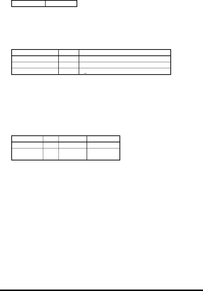
8. MECHANICAL SPECIFICATIONS
8.1 Dimension
Width 69.85mm ( 2.75” )
Height 9.5 mm ( 0.37”)
Depth 100.0 mm ( 3.94” )
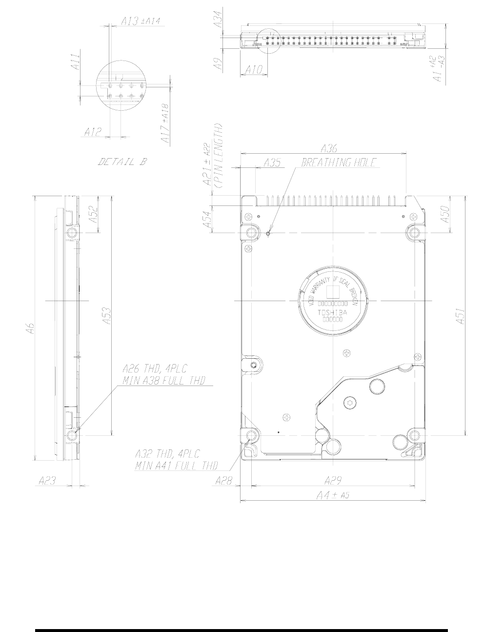
Figure 1 and Table 8.4-1 show an outline of the drive.
8.2 Weight
MK1032GAX 101 gram (typ. ) / 102 gram(max.)
8.3 Drive Orientation
The drive can be installed in all axes (6 directions).
8.4 Mounting Instructions
●Take anti-static measures in order to avoid damage to the drive when handling it.
The drive uses parts susceptible to damage due to ESD (electrostatic discharge).
Wear ESD proof wrist strap in accordance with the usage specified when handling
a drive that is not in an anti-static protection bag.
●Extreme shock to the drive may cause damage to it, data corruption, etc..
Do not subject the drive to extreme shock such as dropping, upsetting or crashing
against other objects.
●Do not place objects which generate magnetic fields such as magnets, speakers,
etc. near the drive.
Magnetism may cause damage to the drive or data loss.
NOTE
SAFETY

Toshiba Corporation Digital Media Network Company
Page 18 of 159
© 2004, Copyright TOSHIBA Corporation All Rights Reserved
8.4.1 Screwing
Four screws should be tightened equally with 0.39 N.m ( 4 kgf.cm ) torque. The depth should be 3.0 mm
min. and 3.5 mm maximum.
8.4.2 Installation
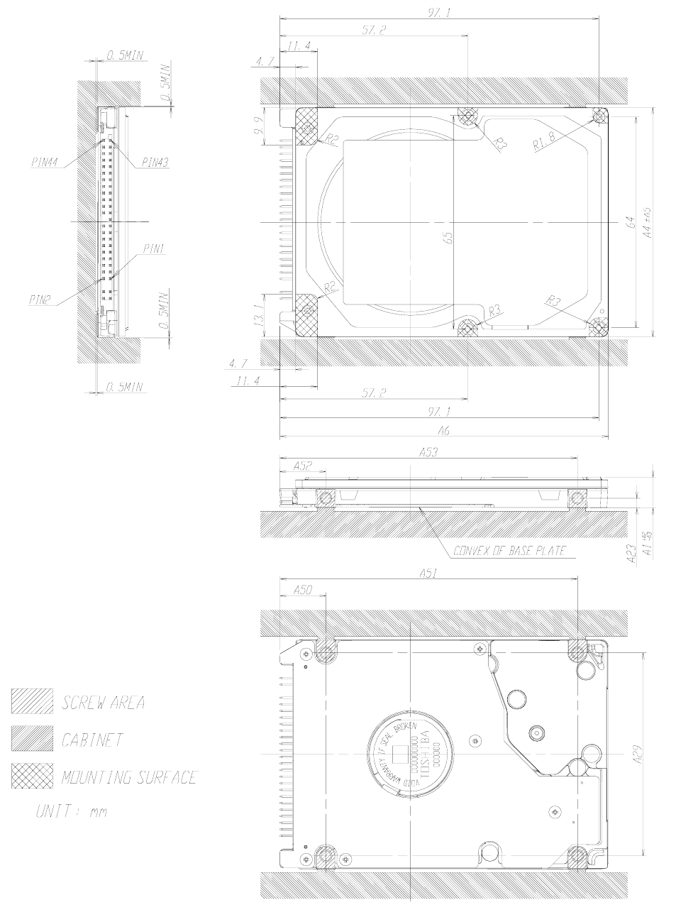
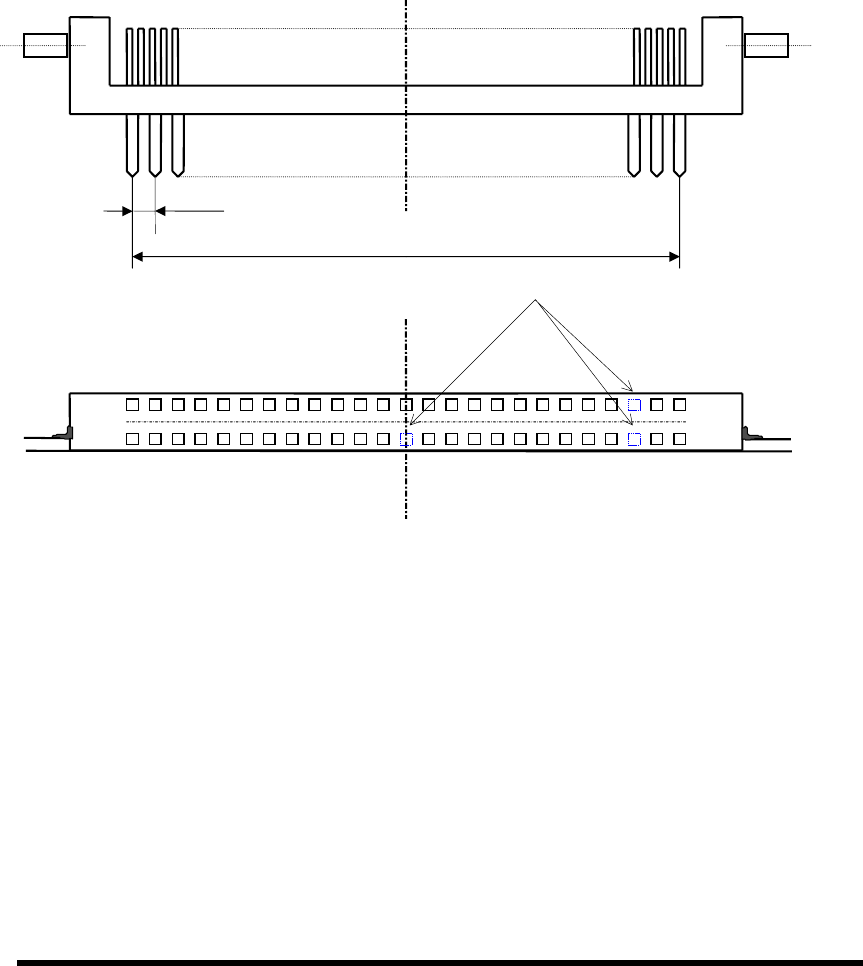
① The drive should be mounted carefully on the surface of 0.1mm or less flatness to avoid excessive
distortion.
② In order to prevent short-circuit under any circumstances, the space of 0.5mm or more should be kept
under the PCB and the design have to be checked carefully (See fig. 2).
③ Enough space should be kept around the drive especially around the convex portion of HDA (See fig. 2) to
avoid any contact with other parts, which may be caused by receiving shock or vibration.
④ The temperature of the top cover and the base must always be kept under 63℃ to maintain the required
reliability. ( If the drive runs continuously or spins-up frequently, the temperature of the top cover may rise to
15℃ maximum. If the drive is used in ambient temperature of 48℃ or more, it should be kept where
adequate ventilation is available to keep the temperature of top cover under 63℃)
⑤ M3 mounting screw holes are tapped directly on the base for electrical grounding between the drive and the
base. In order to prevent the drive performance from being affected by the system noise, appropriate
evaluation should be conducted before deciding loading method.
⑥ Be sure not to cover the breathing hole ( See fig. 1) to keep the pressure inside the drive at a certain level.
⑦ Do not apply force exceeding 2[N] on the Top Cover.
⑧ The drive contains several parts which may be easily damaged by ESD(Electric Static Discharge). Avoid
touching the interface connector pins and the surface of PCB. Be sure to use ESD proof wrist strap when
handling the drive.
⑨ A rattle heard when the drive is moved is not a sign of failure.
Toshiba Corporation Digital Media Network Company
Page 19 of 159
© 2004, Copyright TOSHIBA Corporation All Rights Reserved
Figure 1 MK1032GAX Dimensions
Toshiba Corporation Digital Media Network Company
Page 20 of 159
© 2004, Copyright TOSHIBA Corporation All Rights Reserved
Table 8.4-1 Dimensions
SFF-8200 Rev1.1(*)
SFF-8201 Rev1.2
SFF-8212 Rev1.2
MK1032GAX
(Differences only)
Dimension Millimeters Inches Millimeters Inches
A1 − − 9.5 0.374
A2 − − 0.20 0.008
A3 − − 0.20 0.008
A4 69.85 2.750
A5 0.25 0.010
A6 101.85 max 4.010 max 100.00 ±0.41 3.973 ±0.016
A9 3.99 0.157
3.99 ±0.43 0.157 ±0.017
A10 10.14 0.399 10.14 ±0.27 0.399 ±0.011
A11 2.00 0.079
A12 2.00 0.079
A13 0.50 0.020
A14 0.05 0.002
A17 0.50 0.020
A18 0.05 0.002
A21 3.86 0.152
A22 0.20 0.008
A23 3.00 0.118
A26 M3 N/A
A28 4.07 0.160
A29 61.72 2.430 61.72 ±0.25 2.430 ±0.010
A32 M3 N/A
A34 1.00 min 0.039 min
A35 8.00 max 0.315 max
A36 60.20 min 2.370 min
A37 8.00 0.315 5.00 0.197
A38 3.00 min 0.118 min 3.50 min 0.137 min
A41 2.50 min 0.980 min 3.50 min 0.137 min
A50 14.00min 0.551min
14.00 ±0.25 0.551 ±0.010
A51 90.60min 3.567min
90.60 ±0.30 3.567 ±0.012
A52 14.00min 0.551min
14.00 ±0.25 0.551 ±0.010
A53 90.60min 3.567min
90.60 ±0.30 3.567 ±0.012
A54 10.24min 0.403min
10.24 ±0.51 0.403 ±0.020
(*)SFF-8200,83021212:Small Form Factor Standard
Toshiba Corporation Digital Media Network Company
Page 21 of 159
© 2004, Copyright TOSHIBA Corporation All Rights Reserved
Figure 2 Mounting Recommendation

Toshiba Corporation Digital Media Network Company
Page 22 of 159
© 2004, Copyright TOSHIBA Corporation All Rights Reserved
9. ENVIRONMENTAL LIMITS
9.1 Temperature and Humidity
9.1.1 Temperature
Operating 5
oC- 55oC
Gradient 20
oC / Hour maximum
Non- operating - 20oC- 60oC
Gradient 20
oC / Hour maximum
Under shipment - 40oC- 70oC
Gradient 30
oC / Hour maximum
( Packed in Toshiba’s original shipping package. )
The temperature of top cover and base must be kept under 63℃ at any moment to maintain the desire
reliability.
9.1.2 Humidity
Operating 8%- 90% R.H. ( No condensation. )
Non- operating 8%- 90% R.H. ( No condensation. )
Under shipment 5%- 90% R.H. ( Packed in Toshiba’s original shipping package. )
Max. wet bulb 29oC (Operating)
40oC (Non- operating)
9.2 Vibration
Operating 9.8 m/s2 ( 1.0G )
5- 500 Hz
Sine wave sweeping 1 oct./ minute
No unrecoverable error.
Non operating 10.0 mm p-p displacement.
5-15 Hz
No unrecoverable error.
49 m/s2 ( 5.0G )
15- 500 Hz
Sine wave sweeping 1 oct./ minute
No unrecoverable error.
9.3 Shock
Operating 3,185 m/s2 ( 325G )
2 msec half sine wave
Repeated twice maximum / second
No unrecoverable error.
Non- operating 8,330 m/s2 ( 850G ) 1msec half sine wave
1,960 m/s2 ( 200G ) 11 msec half sine wave
Repeated twice maximum / second
No unrecoverable error.
Under shipment 70 cm free drop
No unrecoverable error.
Apply shocks in each direction of the drive’s three
mutually perpendicular axes, one axis at a time.
( Packed in Toshiba’s original shipping package. )
Toshiba Corporation Digital Media Network Company
Page 23 of 159
© 2004, Copyright TOSHIBA Corporation All Rights Reserved
9.4 Altitude
Operating - 300 m to 3,000 m
Non operating - 400 m to 15,000 m
9.5 Acoustics
(
Sound Power
)
25 dBA Average For idle mode ( Spindle in rotating ).
28 dBA Average Randomly select a track to be sought in such a way that every track
has equal probability of being selected.
Seek rate(nS) is defined by the following formula:
n
S = 0.4 / ( tT + tL )
t
T is published time to seek from one random track to another
without including ratational latency;
t
L is the time for the drive to ratate by half a revolution.
Measurements are to be taken in accordance with ISO 7779.
9.6 Safety Standards
The drive satisfies the following standards .
MK1032GAX
Underwriters Laboratories (UL)60950
Canadian Standard Association (CSA)C22.2 No.60950-00
TUV Rheinland EN 60950
Bureau of Standards,
Metrology and Inspection D33003
Ministory of Information and
Communication (Note 1)
(Note 1) Marks of ministory of information and communication
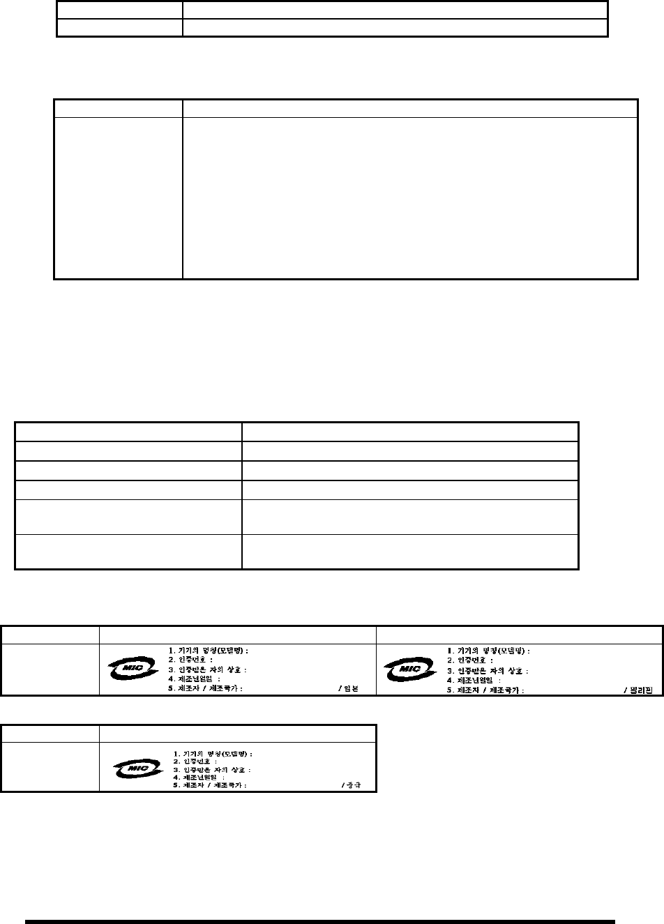
Made in Japan Made in Philippines
Made in China
MK1032GAX
E-H011-04-3279(B)
TOSHIBA CORPORATION
2004-8
TOSHIBA CORPORATION
MK1032GAX
E-H011-04-3279(B)
TOSHIBA CORPORATION
2004-8
TOSHIBA CORPORATION
MK1032GAX
E-H011-04-3279(B)
TOSHIBA CORPORATION
2004-8
TOSHIBA CORPORATION
Toshiba Corporation Digital Media Network Company
Page 24 of 159
© 2004, Copyright TOSHIBA Corporation All Rights Reserved
9.7 EMC Adaptability
The drive satisfies the following standards .
MK1032GAX
EN5008M1-E1 EN55022:1998 Class B
EN50081-1 EN61000-3-2 1995
EN61000-3-3 1995
EN55024 EN61000-4-2 1995
EN61000-4-3 1998
ENV50204 1995
EN61000-4-4 1995
EN61000-4-5 1995
EN61000-4-6 1996
EN61000-4-11 1994
9.8 Magnetic Fields
The disk drive shall work without degradation of the soft error rate under the following Magnetic Flux Density
Limits at the enclosure surface.
MK1032GAX 0.6mT (6 Gauss)
Toshiba Corporation Digital Media Network Company
Page 25 of 159
© 2004, Copyright TOSHIBA Corporation All Rights Reserved
10. RELIABILITY
A failure is defined as an inability of the drive to perform its specified function described in the requirements
of this document when being operated under the normal conditions or conditions specified in this document.
However , damages caused by operation mistake, mishandling, accidents, system errors and other
damages that can be induced by the customers are not defined as failure.
.
10.1 Error Rate
10.1.1 Non- Recoverable Error Rate
1 error per 1013 bits read
The defective sectors allocated to the spare locations in the factory are not counted in the error rate.
10.1.2 Seek Error Rate
1 error per 106 seeks
A seek error is a positioning error recoverable by a retry including recalibration.
10.2 Mean Time to Failure (MTTF)
A failure means that the drive can not execute the function defined in this document under the nominal
temperature, humidity and the other conditions specified in this document . Damages caused by operation
mistake, mishandling, system failure and other damages occurred under the conditions which are not
described in this document are not considered as the failure.
MTTF 300,000 hours
Conditions
Power on hours 2,800 hours ( 200 days x 14 hours ) / year)
Operating hours 600 hours ( 200 days x 3 hours ) / year)
Seek hours 1.30 x 10⁶ seeks / month
Number of load / unload 70 times / hour ( 60,000 times / year )
Environment Normal ( 25oC, 101.3 kPa ( 1,013 mb ) )
10.3 Product Life
5 years or 20,000 power on hours whichever comes earlier
10.4 Repair
A defective drive should be replaced. Parts and subassemblies should not be repaired individually .
10.5 Preventive Maintenance (PM)
No preventive maintenance is required.

Toshiba Corporation Digital Media Network Company
Page 26 of 159
© 2004, Copyright TOSHIBA Corporation All Rights Reserved
10.6 Load/Unload
Be sure to issue and complete the following commands for unloading before cutting off the power
supply.
Following table shows the specification for normal load/unload cycles.
Load/unload cycle (Times) Environment
600,000 Room temperature
300,000 Operational temperature range
Unload is executed by the following commands :
・Standby
・Standby Immediate
・Sleep
・Hard reset
Load/unload is also executed as one of the idle modes of the drive.
If the power supply is cut when the head is on a media, Emergency Unload is performed by routing the
back-EMF of SPM to the voice coil. In this case, Emergency Unload is performed 20,000 times
maximum. Emergency Unload should be used only when the host-system cannot perform normal
operation.
Toshiba Corporation Digital Media Network Company
Page 27 of 159
© 2004, Copyright TOSHIBA Corporation All Rights Reserved
11. HOST INTERFACE
Related Standards
Information technology - AT Attachment Interface with Extensions (ATA-2)
X3T10.279-199x
Information technology - AT Attachment-3 Interface (ATA-3)
X3T10/2008D Revision 6 October 26, 1995
Information technology - AT Attachment with Packet Interface Extension (ATA -4)
T13/1153D Revision 17 October 30, 1997
Information technology - AT Attachment with Packet Interface-5 (ATA-5)
T13/1321D Revision 3 February 29, 2000
Information technology - AT Attachment with Packet Interface-6 (ATA-6)
T13/1410D Revision 3b February 26, 2002
11.1 Cabling
11.1.1 Interface Connector
Drive side
connector Yamaichi GAP050K11617 or equivalent
Recommended
host side
connector
for board straight type : Berg 86455-044 86456-044
or equivalent
for cable Berg 89361-044 or equivalent
11.1.2 Cable
The following table shows preferable twisted pair type of cable .
Standard diameter 0.32 mm ( 28 AWG )
Characteristics impedance 100- 132 Ω
Toshiba Corporation Digital Media Network Company
Page 28 of 159
© 2004, Copyright TOSHIBA Corporation All Rights Reserved
11.2 Electrical specification
11.2.1 Cable length and capacitance
0.46m MAX. 35pF MAX.
11.2.2 DC input/output Characteristics
11.2.2.1 Input
item unit value
voltage high (note 1) V 2.0 to (supply voltage +0.5 )
low V -0.3 to 0.8
leak current µA + 10 (note 2)
As non-connected logic voltage, input voltage level is from -0.3V to 0.5V.
(note 1) The max. input range of signal is from -0.3V to (supply voltage +0.5V )
(note 2) Except for signal lines pulled up as shown inTable 11.3-1
11.2.2.2 Output
item unit value note
voltage high V 2.4 min. IOH = - 1mA
low V 0.4 max.
0.4 max. IOL = 4mA
IOL = 8mA
Toshiba Corporation Digital Media Network Company
Page 29 of 159
© 2004, Copyright TOSHIBA Corporation All Rights Reserved
11.3 Interface connector
11.3.1 ATA interface connector
Figure 3 ATA interface connector
Polarity key
43
44
1
2
2.00
2.00
×
24 = 48.00

Toshiba Corporation Digital Media Network Company
Page 30 of 159
© 2004, Copyright TOSHIBA Corporation All Rights Reserved
11.3.2 Pin Assignment
The following table describes all of the pins on the Task File Interface.
Table 11.3-1 Signal pin assignment
PIN No. SIGNALS PIN No. SIGNALS
1 - RESET 2 GROUND
3 DD 7 4 DD 8
5 DD 6 6 DD 9
7 DD 5 8 DD 10
9 DD 4 10 DD 11
11 DD 3 12 DD 12
13 DD 2 14 DD 13
15 DD 1 16 DD 14
17 DD 0 18 DD 15
19 GROUND 20 KEY
21 DMARQ 22 GROUND
23 - DIOW 24 GROUND
STOP
25 -DIOR 26 GROUND
-DMARDY
HSTROBE
27 IORDY 28 CSEL
-DMARDY
-DSTROBE
29 -DMACK 30 GROUND
31 INTRQ 32 - IOCS16
33 DA 1 34 - PDIAG/-CBLID
35 DA 0 36 DA 2
37 - CS0 38 - CS1
39 - DASP 40 GROUND
41 + 5V 42 + 5V
43 GROUND 44 RESERVED
Note) Symbol (-) in front of signal name shows negative logic.

Toshiba Corporation Digital Media Network Company
Page 31 of 159
© 2004, Copyright TOSHIBA Corporation All Rights Reserved
11.3.3 Signal Treatment
Driver types and requirements for the signal pull- up and down are as follows. Resistor requirement is minimum for the
host. - IO16 is pulled up in the drive with certain value so that the Vol is obtained to run with a host that has large value of
pull up resistor. - CS0 and - CS1 are also pulled up for better noise immunity.
Table 11.3-2 Signal treatment
SIGNAL Driven by TYPE By host By drive
- RESET host TP 10kΩPU
DD 0:15
b
i-direction TS
DMAR
Q
drive TS 5.6 k
Ω
PD
- DIOR hos
t
TS
-DMARDY
HSTROBE
- DIOW hos
t
TS
STOP
IORDY drive TS 4.7 k
Ω
PU
-DDMARDY
DSTROBE
CSEL hos
t
GND 10 k Ω PU
- DMACK hos
t
TP
INTR
Q
drive TS 10 k
Ω
PD
- IOCS16 drive OD 1.0 k
Ω
PU 1.2 k Ω PU
DA 0:2 hos
t
TP
- PDIAG/drive TS 10 k Ω PU
- CS0 - CS1 hos
t
TP
- DASP drive OD 10 k Ω PU
TP = Totem Pole, TS = Tri-State, PD = Pull Down, PU = Pull-Up, OD = Open Drain
Toshiba Corporation Digital Media Network Company
Page 32 of 159
© 2004, Copyright TOSHIBA Corporation All Rights Reserved
11.3.4 Series resistance
Each signal has its own series resistance.
SIGNAL SERIAL RESISTANCE VALUE
-DIOR 82Ω
-HDMARDY
HSTROBE
-DIOW 82Ω
STOP
-CS0, -CS1 82Ω
DA0,DA1,DA2 82Ω
-DMACK 82Ω
DMARQ 22Ω
INTRQ 22Ω
IORDY
-DDMARDY
DSTROBE
22Ω
DD0∼DD15 33Ω
11.3.5 Signal Description
SIGNAL DIR. PIN DESCRIPTION
- RESET O (*1) 1 Reset signal from the host system; It shall be active low when system is
powered-up or when voltage fault is detected.
DD 15- 0 I/O 18- 3 16 bit bi- directional data bus between the host system and the drive. All 16 bits
are used for data transfer in the data register. The lower 8 bits, HD0- HD7, are
used for the other register and ECC access.
KEY N/C 20 Pin position 20 has no connection pin, clipped on the drive and plugged on the
cable in order to ensure correct orientation of the cable and to avoid wrong
insertion.
DMARQ I 21 DMA request signal is set by the drive to indicate that the DMA data transfer is
ready. The direction of the data transfer is controlled by write/read strobe signal
(HOST IOW or HOST IOR). This signal is used on a hand shake manner with -
DMACK.
- DIOW
STOP
O 23 Write strobe. The rising clocks data from the host data bus, HD0 through HD15 to
a register or data register of the drive.
Stop signal used by the host after the completion of Ultra DMA Burst.
- DIOR
-HDMARDY
HSTROBE
O 25 Read strobe. When active low, this signal enables data from a register or the data
of the drive onto the host data bus, HD0 through HD15. The rising edge of
-HOST IOR latches on the data on the bus from the drive.
This signal is for reporting the drive that the host system is ready to accept Ultra
DMA data.
Strobe. HSTROBE indicates that the host transfers ULTRA DMA data. The rising
edge and the falling edge of HSTROBE enable the drive to latch the data.
IORDY
-DDMARDY
DSTROBE
I 27 IORDY reports host that the BUS is available.
-DDMARDY is asserted to indicate that the drive is ready to receive the Ultra DMA
data.
Strobe. DSTROBE is asserted to indicate that the drive transfers Ultra DMA data.
The rising edge and falling edge of DSTROBE enable the host to latch the data.

Toshiba Corporation Digital Media Network Company
Page 33 of 159
© 2004, Copyright TOSHIBA Corporation All Rights Reserved
CSEL O 28 If jumper pins B through D are assigned, Drive0/Drive1 setting with this pin is
valid. When grounded, the drive recognizes itself as a Drive0. When not
grounded, the drive recognizes itself as a Drive1.
- DMACK O 29 Responding to DMARQ, this signal indicates that the host is ready to receive or
send the data.
INTRQ I 31 Interrupt to the host system, enabled only when the drive is selected and the host
activates the - IEN bit in the Device Control register. When the - IEN bit is inactive
or the drive is not selected, this output is in a high impedance state, whether an
interrupt is set or not.
The interrupt is set when the IRQ bit is set by the drive CPU. IRQ is reset to zero
when host reads the Status register or a write to the command register or when
DRQ is negated.
- IOCS16 I 32 Indication to the host system that the 16 bit data register has been addressed and
that the drive is ready to send or receive a 16 bit data word (open drain).
DA 1 O 33 Address line from the host system to select the registers of the drive.
- PDIAG
/- CBLID
I/O 34 In Drive0/Drive1 mode, this signal reports the presence of Drive1 drive to Drive0
and enables transmitting of diagnostic result between Drive0 and Drive1
DA 0 O 35 Address line from the host system to select the registers of the drive.
DA 2 O 36 Address line from the host system to select the registers of the drive.
- CS0 O 37 Chip select signal generated from the host address bus. This signal is used to
select one of the two groups of host accessible registers.
- CS1 O 38 Chip select signal generated from the host address bus. This signal is used to
select one of the two groups of host accessible registers.
- DASP I 39 This is a signal from the drive used either to drive an external LED whenever the
drive is being accessed, or to report presence of the Drive1 to the Drive0 when the
drive is in Drive0/Drive1 mode.
RESERVED 27,44 Reserved for future use. No connection.
+ 5V 41, 42 5V power line. 41pin and 42pin are connected within the drive.
GROUND 2,19
22,24
26,30
40,43
Ground between the drive and the host system.
(*1) ‘I’ is from the drive to the host system, ‘O’ is from the host system to the drive, and ‘I/O’ is bi-directional.
Toshiba Corporation Digital Media Network Company
Page 34 of 159
© 2004, Copyright TOSHIBA Corporation All Rights Reserved
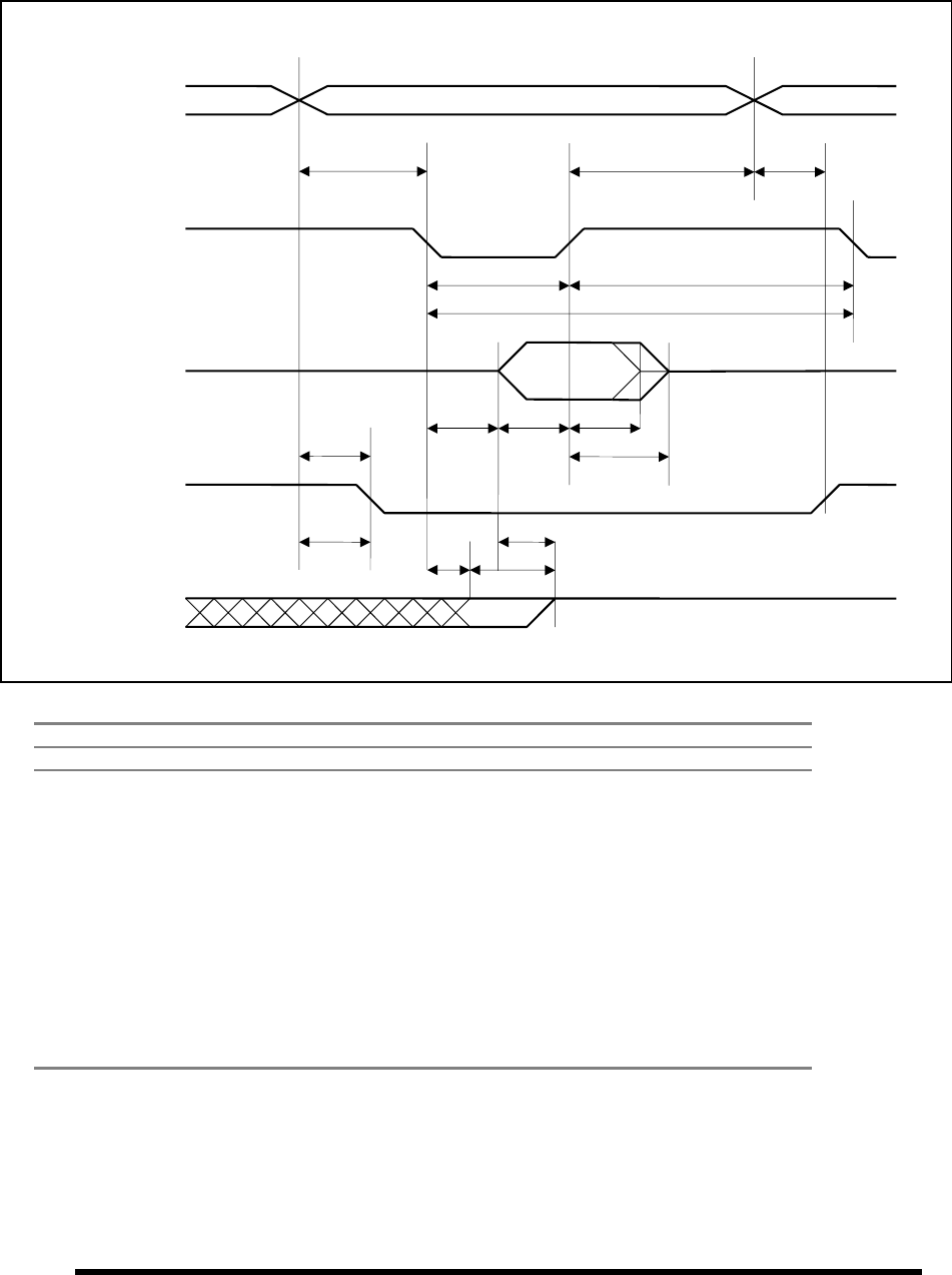
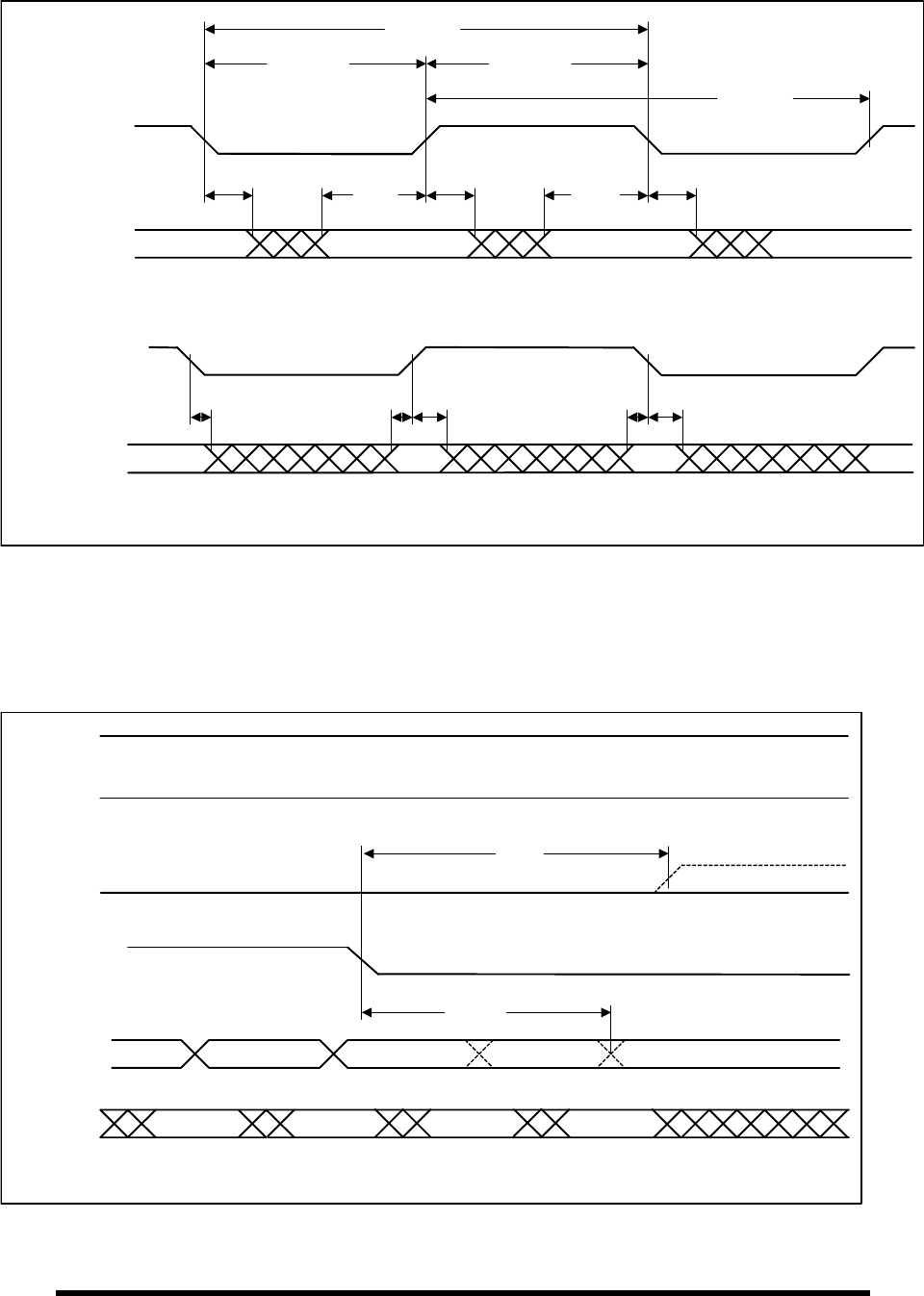
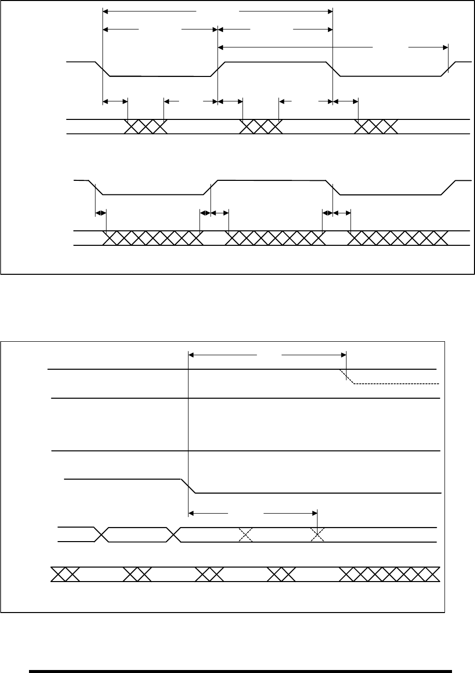
11.4 Host Interface Timing
11.4.1 Program I/O Write Timing
Transfer mode
Symbol Meaning 0 1 2 3 4
t
ASW Address Setup to -DOW Low (min.) 70 50 30 30 25
t
DS Data Setup to -DOW High (min.) 60 45 30 30 20
t
WE -DOW Pulse Width (min.) 165 125 100 80 70
t
DH Data Hold from -DOW High (min.) 30 20 15 10 10
t
AHW ADDR Hold from -DOW High (min.) 20 15 10 10 10
t
WER -DOW Inactive (min.) - - - 70 25
t
WCY Write Cycle Time (min.) 600 383 240 180 120
t
CICSV -IOCS16 valid from -CS (max.) 90 50 40 n/a* n/a*
t
AICSV -IOCS16 valid from address (max.) 90 50 40 n/a* n/a*
t
AICSI -IOCS16 inactive from address (max.) 60 45 30 n/a* n/a*
t
A IORDY Setup time (max.) 35 35 35 35 35
t
B IORDY Pulse Width (max.) 1250 1250 1250 1250 1250
(*) -IOCS16 shall be specified in ATA-2 specifications. For other modes, this signal is invalid. The Drive
releases -IOCS16 within the time of tAICSI, but how much time it takes to turn to inactive condition is
determined by pull up resistance, output impedance and line capacitance.
tASW tAHW tAICSI
tAtB
tAICSV
tCICSV tDS tDH
tWCY
tWER
tWE
DA2, DA1, DA0
-CS0, -CS1
-DIOW
DD15∼DD0
-IOCS16
IORDY
Toshiba Corporation Digital Media Network Company
Page 35 of 159
© 2004, Copyright TOSHIBA Corporation All Rights Reserved
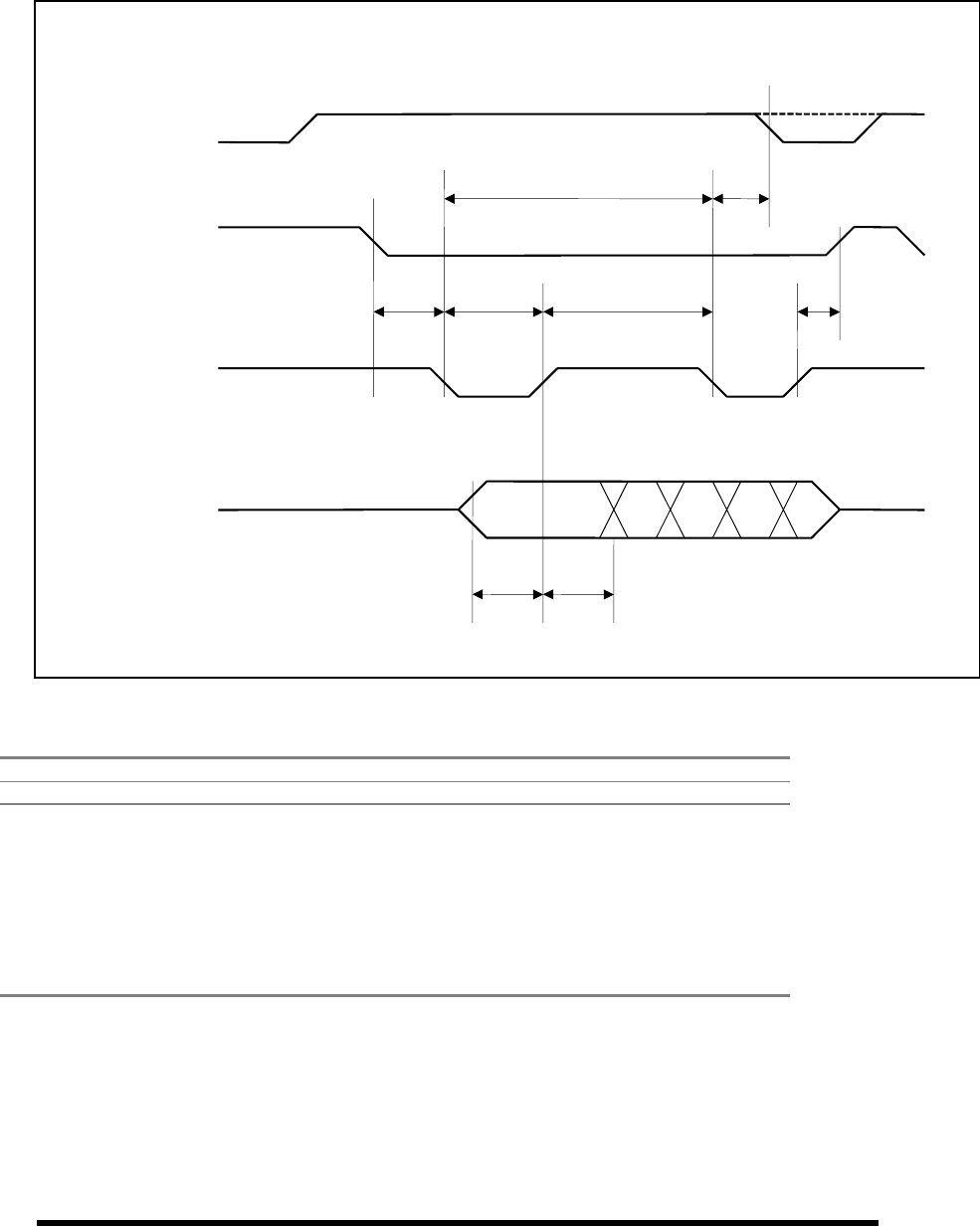
11.4.2 Program I/O Read Timing
Transfer mode
Symbol Meaning 0 1 2 3 4
t
ASE Address Setup to -DIOR Low (min.) 70 50 30 30 25
t
RE -DIOR Pulse Width (min.) 165 125 100 80 70
t
RDSE -DIOR data setup (min.) 50 35 20 20 20
t
DOH Data Hold from -DIOR High (min.) 5 5 5 5 5
t
HDTS Data Tri-state from -DIOR High (max.) 30 30 30 30 30
t
AHE ADDR Hold from -DIOR High (min.) 20 15 10 10 10
t
RDR -DIOR Inactive (min.) - - - 70 25
t
RDCY Read Cycle Time (min.) 600 383 240 180 120
t
CICSV -IOCS16 valid from -CS (max.) 90 50 40 n/a* n/a*
t
AICSV -IOCS16 valid from address (max.) 90 50 40 n/a* n/a*
t
AICSI -IOCS16 inactive from address (max.) 60 45 30 n/a* n/a*
t
RD Read Data Valid to IORDY (min.) 0 0 0 0 0
t
A IORDY Setup time (max.) 35 35 35 35 35
t
B IORDY Pulse Width (max.) 1250 1250 1250 1250 1250
(*) -IOCS16 is specified in ATA-2 specifications. For other modes, this signal is invalid. Drive releases
-IOCS16 within the time of tAICSI, but how long it takes to turn to inactive condition is defined by pull up
resistance, output impedance and line capacitance.
tASE tAHE tAICSI
tAtB
tAICSV
tCICSV
tRDSE tDOH
tRDCY
tRDR
tRE
DA2, DA1, DA0
-CS0, -CS1
-DIOR
DD15∼DD0
-IOCS16
IORDY
tHDTS
tDAC
tRD
Toshiba Corporation Digital Media Network Company
Page 36 of 159
© 2004, Copyright TOSHIBA Corporation All Rights Reserved
11.4.3 Multiword DMA Write Timing
ATA/ATAPI-6 SPECIFICATIONS
Transfer mode MODE 0 MODE 1 MODE 2
Symbol Meaning Min. Max. Min. Max. Min. Max.
t0 Cycle time 480 150 120
t
C DMACK to DMARQ delay --- --- ---
t
D -DIOW 16-bit 215 80 70
t
G -DIOW data setup 100 30 20
t
H -DIOW data hold 20 15 10
t
I DMACK to -DIOW setup 0 0 0
t
J -DIOW to DMACK hold 20 5 5
t
K -DIOW negated pulse width 215 50 25
t
L -DIOW to DMARQ delay 40 40 35
tG
tL
-DMACK
tH
tKtJ
tI
DMARQ
-DIOW
DD15∼DD0
tO
tD
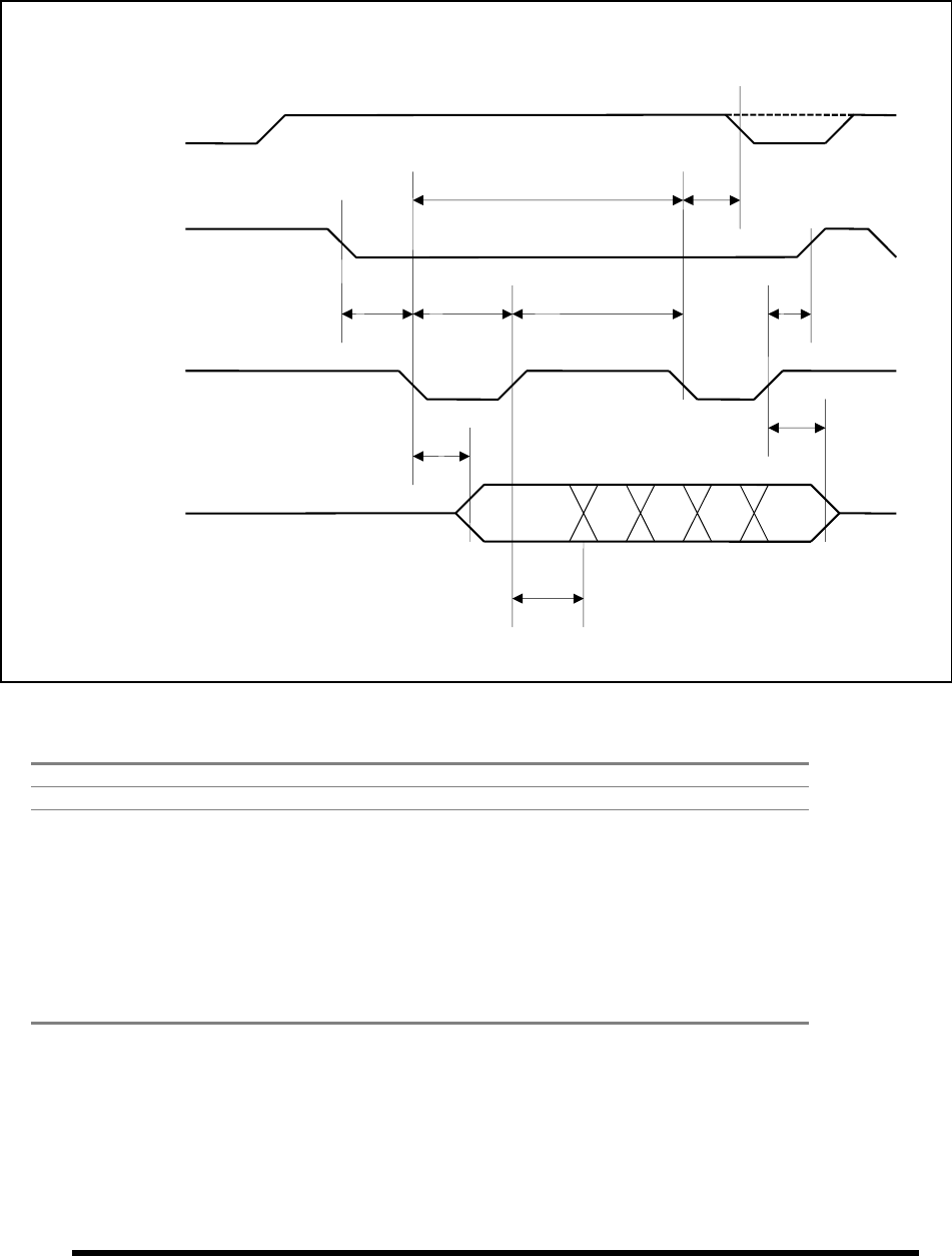
Toshiba Corporation Digital Media Network Company
Page 37 of 159
© 2004, Copyright TOSHIBA Corporation All Rights Reserved
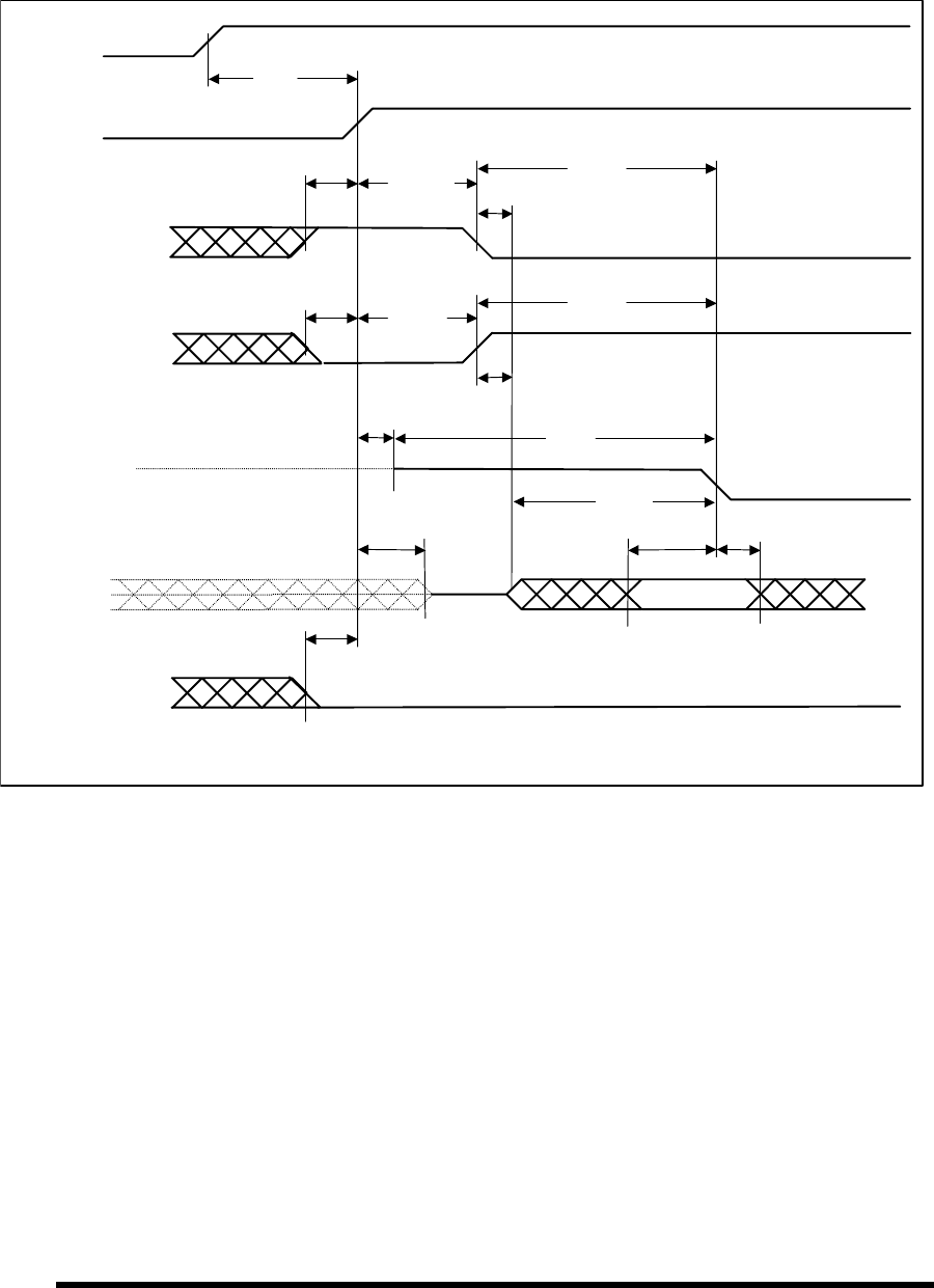
11.4.4 Multiword DMA Read Timing
ATA/ATAPI-6 SPECIFICATIONS
Transfer mode MODE 0 MODE 1 MODE 2
Symbol Meaning Min. Max. Min. Max. Min. Max.
t0 Cycle time 480 150 120
t
C DMACK to DMARQ delay --- --- ---
t
D -DIOR 16-bit 215 80 70
t
E -DIOR data access 150 60 50
t
F -DIOR data hold 5 5 5
t
Z -DIOR to tristate 20 25 25
t
I DMACK to -DIOR setup 0 0 0
t
J -DIOR to DMACK hold 20 5 5
t
K -DIOR negated pulse width 50 50 25
t
L -DIOR to DMARQ delay 120 40 35
tE
tL
-DMACK
tF
tKtJ
tI
DMARQ
-DIOR
DD15∼DD0
tO
tD
tZ
Toshiba Corporation Digital Media Network Company
Page 38 of 159
© 2004, Copyright TOSHIBA Corporation All Rights Reserved
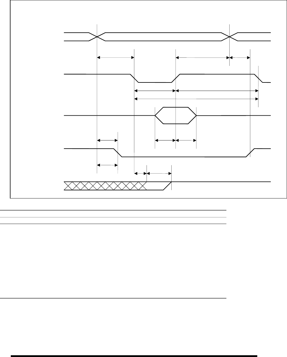
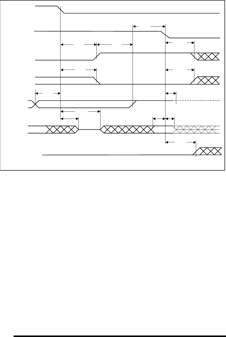
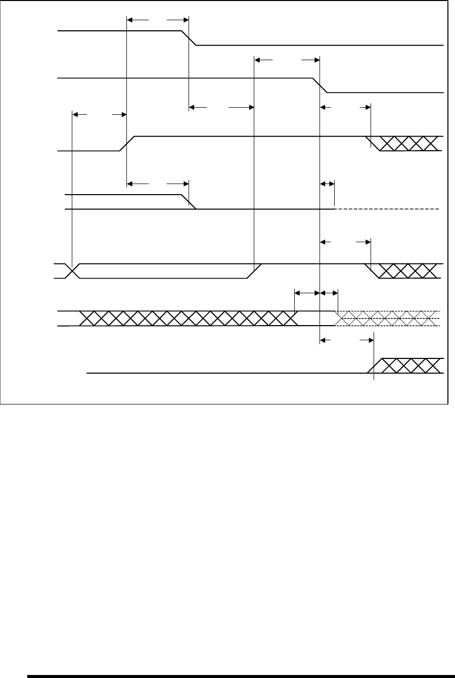
11.4.5 Ultra DMA Timing
Initiating an Ultra DMA data in burst
DMARQ
(device)
DMACK-
(host)
STOP
(host)
HDMARDY-
(host)
DSTROBE
(device)
DD(15:0)
tZAD
DA0, DA1, DA2,
CS0-, CS1-
tUI
tZAD
tACK
tACK
tENV
tENV
tZIORDY
tFS
tFS
tDVS
tAZ tDVH
tACK
tZFS
tDZFS
Toshiba Corporation Digital Media Network Company
Page 39 of 159
© 2004, Copyright TOSHIBA Corporation All Rights Reserved
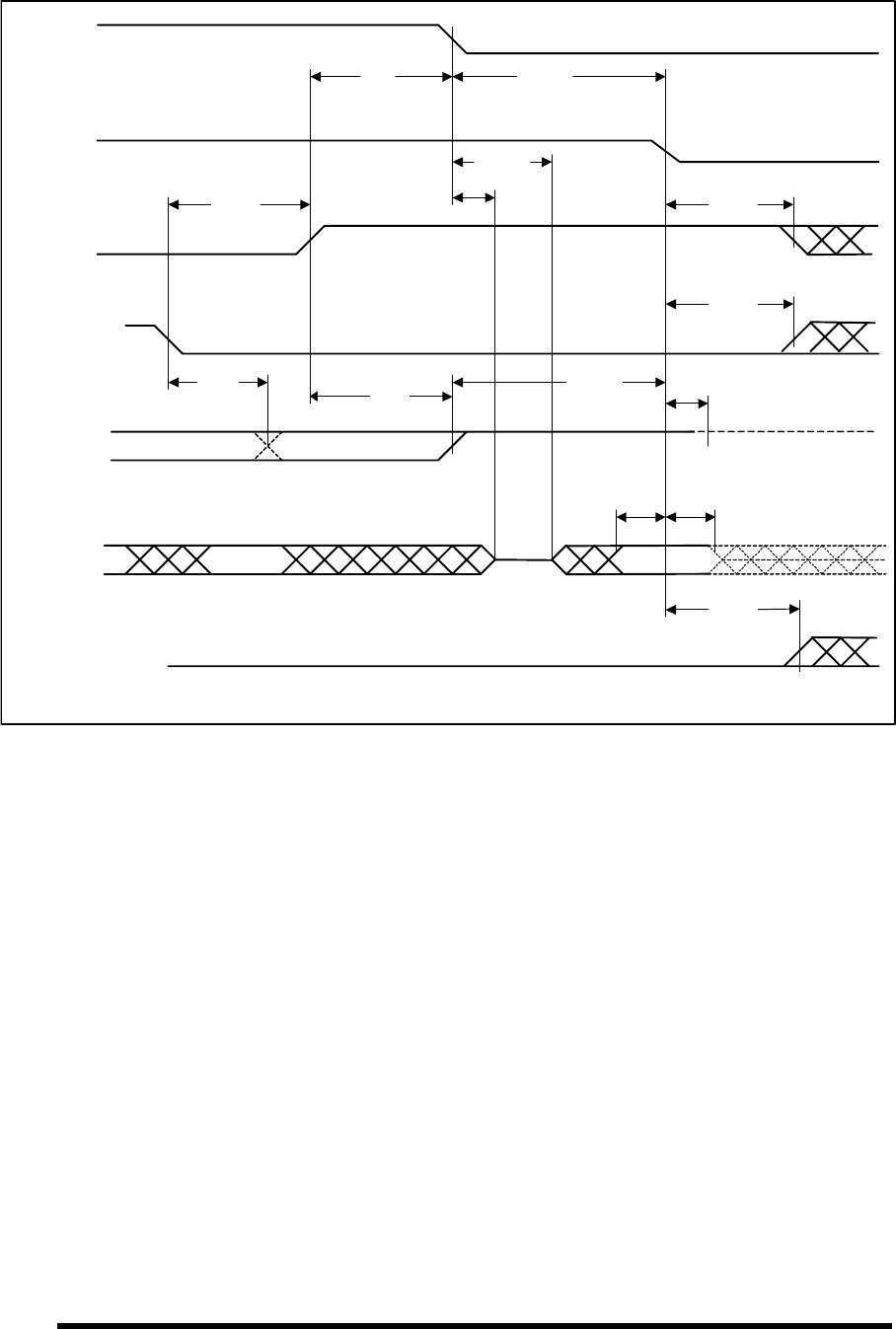
Sustained Ultra DMA data in burst
tDVH
tDVHIC
DSTROBE
at device
DD(15:0)
at device
DSTROBE
at host
DD(15:0)
at host
tCYC tCYC
tDVS
tDVSIC
tDH
tDHIC tDS
tDSIC
t2CYC
t2CYC
tDVH
tDVHIC
tDVH
tDVHIC
tDVS
tDVSIC
tDH
tDHIC
tDH
tDHIC
tDS
tDSIC
Host pausing an Ultra DMA data in burst
DMARQ
(device)
DMACK-
(host)
STOP
(host)
HDMARDY-
(host)
DSTROBE
(device)
DD(15:0)
(device)
tRFS
tRP
Toshiba Corporation Digital Media Network Company
Page 40 of 159
© 2004, Copyright TOSHIBA Corporation All Rights Reserved
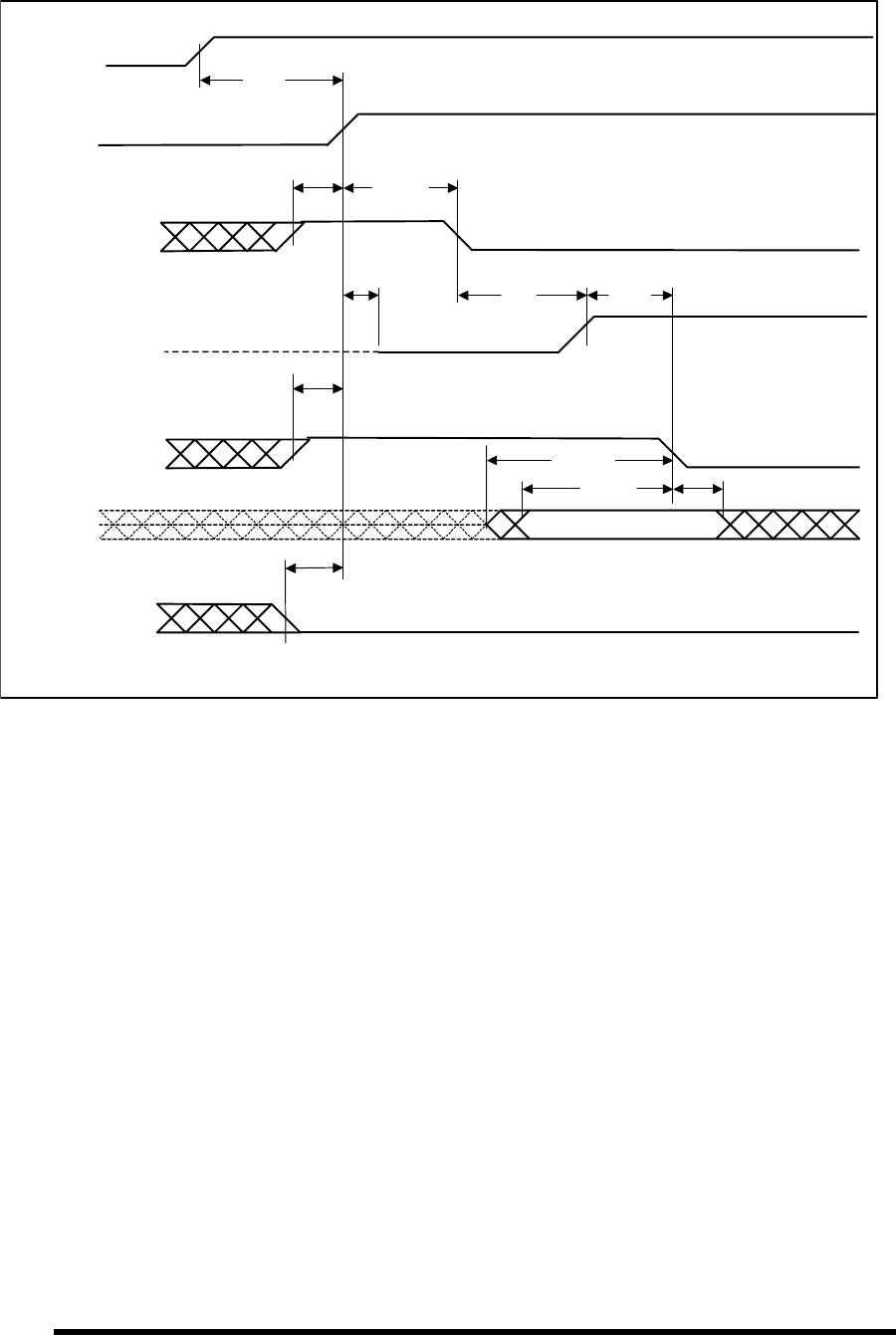
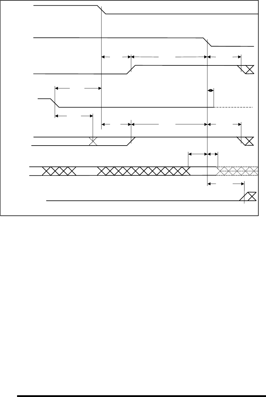
Device terminating an Ultra DMA data in burst
tAZ
tIORDYZ
CRC
DMARQ
(device)
DMACK-
(host)
STOP
(host)
HDMARDY-
(host)
DSTROBE
(device)
DD(15:0)
DA0, DA1, DA2,
CS0-, CS1-
tACK
tLI
tMLI
tCVS
tLI
tACK
tACK
tZAH
tCVH
tSS
tLI
Toshiba Corporation Digital Media Network Company
Page 41 of 159
© 2004, Copyright TOSHIBA Corporation All Rights Reserved
Host terminating an Ultra DMA data in burst
tCVH
CRC
tAZ
DMARQ
(device)
DMACK-
(host)
STOP
(host)
HDMARDY-
(host)
DSTROBE
(device)
DD(15:0)
DA0, DA1, DA2,
CS0-, CS1-
tACK
tMLI
tLI
tLI tIORDYZ
tACK
tACK
tZAH
tMLI
tCVS
tRFS
tRP
Toshiba Corporation Digital Media Network Company
Page 42 of 159
© 2004, Copyright TOSHIBA Corporation All Rights Reserved
Initiating an Ultra DMA data out burst
DMARQ
(device)
DMACK-
(host)
STOP
(host)
DDMARDY-
(device)
HSTROBE
(host)
DD(15:0)
(host)
DA0, DA1, DA2,
CS0-, CS1-
tUI
tACK tENV
tZIORDY tLI
tDZFS
tDVH
tACK
tACK
tUI
tDVS
Toshiba Corporation Digital Media Network Company
Page 43 of 159
© 2004, Copyright TOSHIBA Corporation All Rights Reserved
Sustained Ultra DMA data out burst
tDH
tDHIC
tDVH
tDVHIC
HSTROBE
at host
DD(15:0)
at host
HSTROBE
at device
DD(15:0)
at device
tCYC tCYC
tDVS
tDVSIC
tDS
tDSIC
t2CYC
t2CYC
tDVH
tDVHIC
tDVH
tDVHIC
tDVS
tDVSIC
tDH
tDHIC
tDH
tDHIC
tDS
tDSIC
Device pausing an Ultra DMA data out burst
DMARQ
(device)
DMACK-
(host)
STOP
(host)
DDMARDY
-(device)
HSTROBE
(host)
DD(15:0)
(host)
tRFS
tRP
Toshiba Corporation Digital Media Network Company
Page 44 of 159
© 2004, Copyright TOSHIBA Corporation All Rights Reserved
Host terminating an Ultra DMA data out burst
DMARQ
(device)
DMACK-
(host)
STOP
(host)
DDMARDY-
(device)
HSTROBE
(host)
DD(15:0)
(host)
DA0, DA1, DA2,
CS0-, CS1-
tACK
tLI
tMLI
tCVS
tLI
tLI
tACK
tIORDYZ
tACK
CRC
tCVH
tSS
Toshiba Corporation Digital Media Network Company
Page 45 of 159
© 2004, Copyright TOSHIBA Corporation All Rights Reserved
Device terminating an Ultra DMA data out burst
DMARQ
(device)
DMACK-
(host)
STOP
(host)
DDMARDY-
(device)
HSTROBE
(host)
DD(15:0)
(host)
DA0, DA1, DA2,
CS0-, CS1-
tACK
tMLI
tCVS
tLI
tLI
tACK
CRC
tCVH
tACK
tIORDYZ
tMLI
tRP
tRFS

Toshiba Corporation Digital Media Network Company
Page 46 of 159
© 2004, Copyright TOSHIBA Corporation All Rights Reserved
ATA/ATAPI specifications
Transfer mode MODE 0 MODE 1 MODE 2 MODE 3 MODE 4 MODE 5
Symbo
l
Meaning Min. Max. Min. Max. Min. Max. Min. Max. Min. Max. Min. Max.
tCYC Cycle time 112 73 54 39 25 16.8
t2CYC Two cycle time 230 153 115 86 57 38
tDS Data setup time 15.0 10.0 7.0 7.0 5.0 4.0
tDH Data hold time 5.0 5.0 5.0 5.0 5.0 4.6
tDVS Data valid setup time 70.0 48.0 31.0 20.0 6.7 4.8
tDVH Data valid hold time 6.2 6.2 6.2 6.2 6.2 4.8
tCS CRC setup time 15.0 10.0 7.0 7.0 5.0 5.0
tCH CRC hold time 5.0 5.0 5.0 5.0 5.0 5.0
tCVS CRC valid setup time 70.0 48.0 31.0 20.0 6.7 10.0
tCVH CRC valid hold time 6.2 6.2 6.2 6.2 6.2 10.0
tZFS Strobe released to driving 0 0 0 0 0 35
tDZFS Data released to driving 70.0 48.0 31.0 20.0 6.7 25
tFS First STROBE time 0 230 0 200 0 170 0 130 0 120 0 90
tLI Limit interlock time 0 150 0 150 0 150 0 100 0 100 0 75
tMLI Interlock time min. 20 20 20 20 20 20
tUI Unlimited interlock 0 0 0 0 0 0
tAZ Allowed to release 10 10 10 10 10 10
tZAH Delay time 20 20 20 20 20 20
tZAD Delay time 0 0 0 0 0 0
tENV Envelope time 20 70 20 70 20 70 20 55 20 55 20 50
tRFS Ready to final Strobe 75 70 60 60 60 50
tRP Ready to pause 160 125 100 100 100 85
tIORDYZ
Pullup before IORDY 20 20 20 20 20 20
tZIORDY
Wait before IORDY 0 0 0 0 0 0
tACK Setup hold for DACK 20 20 20 20 20 20
tSS Strobe to DREQ/Stop 50 50 50 50 50 50
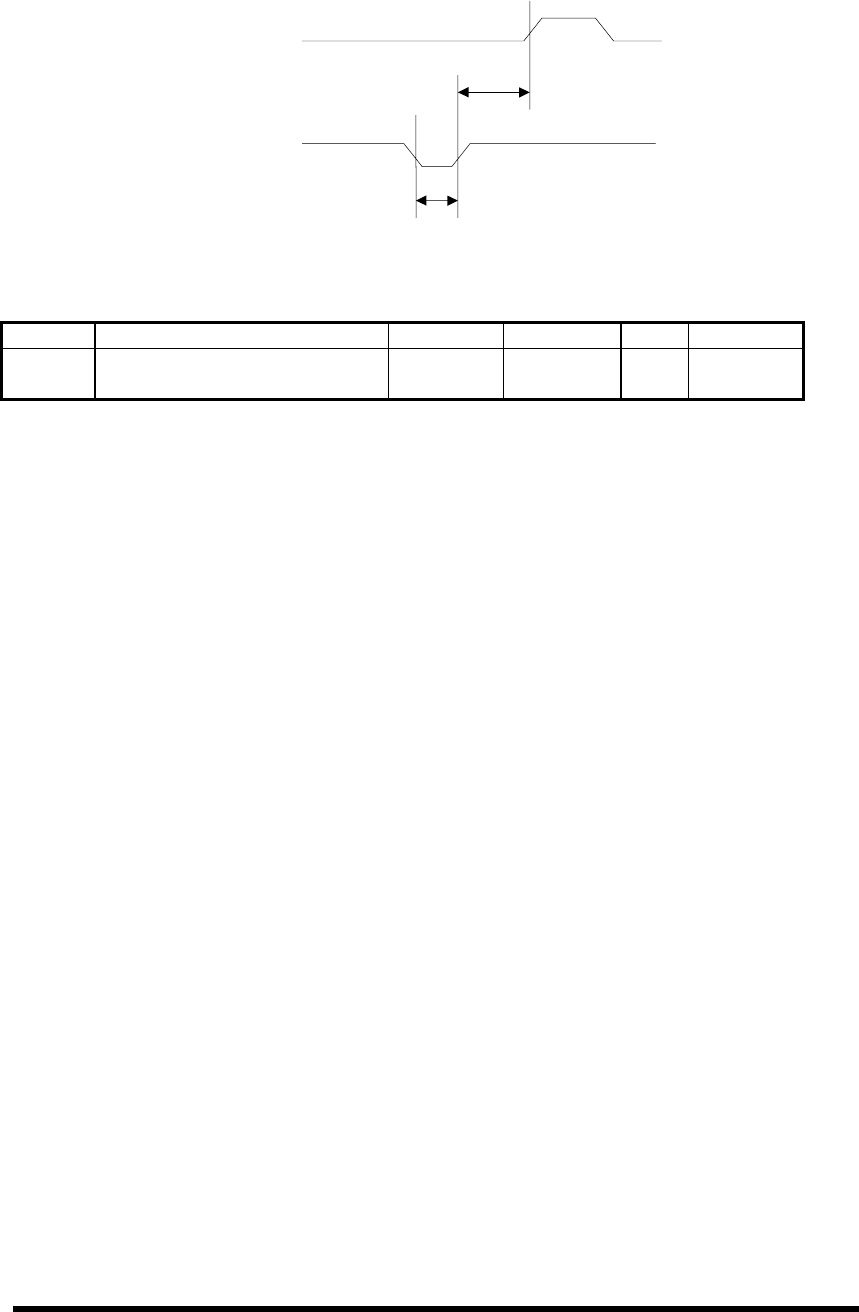
Toshiba Corporation Digital Media Network Company
Page 47 of 159
© 2004, Copyright TOSHIBA Corporation All Rights Reserved
11.4.6 Reset Timing
tM
tN
BUSY
- RESET
Symbol Meaning Minimum Maximum Unit Condition
tM RESET pulse width (Low) 25 µs
tN RESET inactive to BSY active 400 ns
11.5 Grounding
HDA (Head Disk Assembly) and DC ground(ground pins on interface) are connected electrically each other.
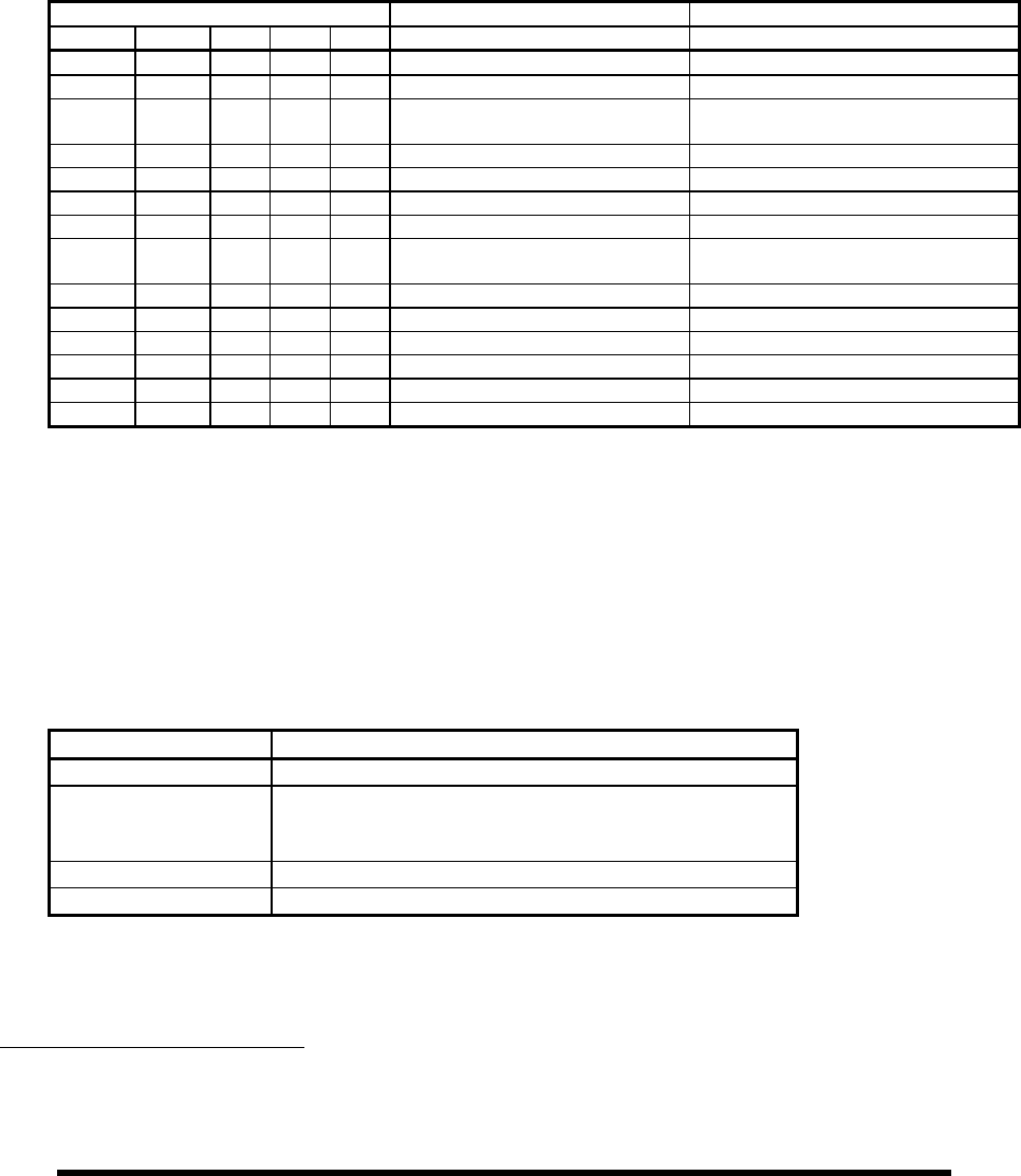
Toshiba Corporation Digital Media Network Company
Page 48 of 159
© 2004, Copyright TOSHIBA Corporation All Rights Reserved
11.6 Address Decoding
The host addresses the drive using programmed I/O. In this method, the required register address should
be placed on the three host address lines, DA2 - DA0. An appropriate chip is selected and a read or write
strode (-DIOR / -DIOW) shall be given to the chip.
The following I/O map shows definitions of all the register addresses and functions for these I/O locations.
The descriptions of each register are shown in the next paragraph.
Table 11.6-1 Register map
Address
- CS0 - CS1 HA2 HA1 HA0 READ REGISTER WRITE REGISTER
0 0 X X X Invalid address Invalid address
0 1 0 0 0 Data register Data register
0 1 0 0 1 Error register Features (Write precompensation)
register
0 1 0 1 0 Sector count Sector count
0 1 0 1 1 Sector number / LBA bit 0- 7 Sector number / LBA bit0-7
0 1 1 0 0 Cylinder low / LBA bit 8- 15 Cylinder low / LBA bit8-15
0 1 1 0 1 Cylinder high / LBA bit16- 23 Cylinder high / LBA bit16-23
0 1 1 1 0 Device head register
/ LBA bit 24- 27 Device head register
/ LBA bit 24-27
0 1 1 1 1 Status register Command register
1 0 0 X X High impedance Not used
1 0 1 0 X High impedance Not used
1 0 1 1 0 Alt. status register Device control register
1 0 1 1 1 Device address register1 Not used
1 1 X X X High impedance Not used
“X” means “don't care”.
The host generates selection of two independent chips on the interface. The selected high order
chip ,-HOST CS1, is valid only when the host is accessing the address of alternate status register, digital
output register , and digital input register respectively. The low order chip, HOST CS0, is used to address all
other registers.
The following table shows the standard decode logic to connect with ISA (Industry Standard Architecture)
bus .
Table 11.6-2 Decode Logic
Register Address Map Decode
1F0-1F7 - CS0 = - ((- A9) (-A3)*(- AEN))
3F6,3F7 - CS1= -
(A9*A8*A7*A6*A5*A*A8*A7*A6*A5*A4*4)*(-A3)*(-
AEN)
170-177 - CS0= - ((- A9)*A8*(- A7)*A6*A5*A4*(- A3)*(- AEN)
376,377 - CS1= - (A9*A8*(- A7)*A6*A5*A4)*(- A3)*(- AEN)
The host data buses 15-8 are valid only when - IOCS16 is active.
• - IOCS16 is asserted when interface address lines match to data register address.
1 ATA-2 Notes: This register is obsolete. A device is not supposed to respond to a read of this address. If a device does
respond, it shall be sure not to drive the DD7 signal to prevent possible conflict with floppy disk implementations.
The drive supports this register to maintain compatibility for ATA-1.

Toshiba Corporation Digital Media Network Company
Page 49 of 159
© 2004, Copyright TOSHIBA Corporation All Rights Reserved
11.7 Register Description
In the following register descriptions, unused write bit should be treated as “don't care”, and unused read
bits should be read as zeros.
11.7.1 Data Register
- CS0 DA2-DA0 : 0 Read / Write
There are seven commands which execute data transfer from/to this register of the sector buffer for Read
and Write operations. The sector table during Format command and the data associated with the Identify
Device command shall also be transferred to this register.
11.7.1.1 Read/Write command
The register provides a high speed 16 bit path into the sector buffer with PIO and DMA.
11.7.1.2 Read/Write Buffer command
This command provides 16 bit path between host and data buffer in the drive.
11.7.1.3 Format command
This command provides a path for the parameter including interleave table in a sector length.
11.7.1.4 Identify Device command
Drive information is transferred during the execution of this command.
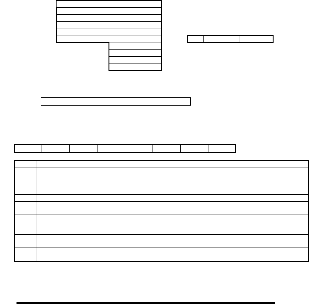
Toshiba Corporation Digital Media Network Company
Page 50 of 159
© 2004, Copyright TOSHIBA Corporation All Rights Reserved
11.7.1.5 Security commands
Password information is transferred during the execution of following four commands.
1) Disable password
2) Erase Unit
3) Set Password
4) Unlock
Data in the register and on the media correspond to each other as follows:
A15 - A8 A7 - A0
transfer 1 D2 D1
transfer 2 D4 D3
: : :
: : :
transfer 256 D512 D511 D1 D2 --- D512 E1 --- E4
transfer 257 E1
: E2
: :
transfer 260 E4
DATA REGISTER DATA FLOW ON THE MEDIA
11.7.2 Error Register
- CS0 DA2-DA0 : 1 Read ONLY
11.7.2.1 Operational Mode
The following descriptions are bit definitions for the operational mode including the error information from the
last command. This command is valid only when the ERROR BIT (bit 0) is set.
ICRC UNC MC IDNF MCR ABRT TK0NF AMNF
Bit 7 Interface CRC error was found during the transfer of Ultra DMA. 2
Bit 6 UNC (Uncorrectable Data Error) – This bit indicates that an uncorrectable error has been encountered in the
data field during a read command.
Bit 5 MC (Media Changed) -- This bit is reserved for use by removable media devices and indicates that new
media is available to the operating system.
Bit 4 IDNF (ID Not Found) --The requested sector could not be found.
Bit 3 MCR (Media Change Requested) is reserved for use by removable media devices and indicates that a
request for media removal has been detected by the device.
Bit 2 ABRT (Aborted Command) -- This bit Indicates that the requested command has been aborted due to the
reason reported in the drive status register (Write Fault, Not Seek Complete, Drive Not Ready, or an invalid
command). The status registers and the error registers may be decoded to identify the cause.
Bit 1 TK0NF (Track 0 Not Found) -- This bit is set to indicate that the track 000 has not been found during a
Recalibrate command.
Bit 0 AMNF (AM Not Found) -- This bit is set to indicate that the required Data AM pattern on read operation has
not been found.
2 ATA-2 Notes: Prior to the development of ATA-2 standard, this bit was defined as BBK (Bad Block Detected) -- This bit was used to
indicate that the block mark was detected in the target’s ID field. The mark does not exist when shipping from the factory.The Mark
will be written by FORMAT command. Read or Write commands will not be executed in any data fields marked bad. The drive does
not support this bit.
Toshiba Corporation Digital Media Network Company
Page 51 of 159
© 2004, Copyright TOSHIBA Corporation All Rights Reserved
11.7.2.2 Diagnostic Mode
The drive enters diagnostic mode immediately after the power -on or after an Execute Diagnostics
command. Error bit in Status Register shall not be set in these cases. The following table shows bit values
for the diagnostic mode.
Table 11.7-1 Diagnostic mode error register
01 No errors
02 Controller register error
03 Buffer RAM error
04 ECC device error
05 CPU ROM/RAM error
06-7F Reserved
8x Drive1 error (see below)
When two drives are daisy-chained on the interface, the Drive0 has valid error information for diagnostic
mode. When the Drive1 detects an error, 80H and OR value (01∼04) diagnosed by the Drive0 are set to
the code above mentioned.
11.7.3 Features Register (Write Precompensation Register)
- CS0 DA2-DA0 : 1 Write only
Write precompensation is automatically optimized by the drive internally. This register is used with Set
Features command.
11.7.3.1 Smart command
This command is used with the Smart commands to select subcommands.
11.7.4 Sector Count Register
- CS0 DA2-DA0 : 2 Read / Write
11.7.4.1 Disk Access command
The sector count register determines the number of sectors to be read or written for Read, Write, and Verify
commands. A 0 in the sector count register specifies a 256 sector transfer. After normal completion of a
command, the content shall be 0.
During a multi-sector operation, the sector count is decremented and the sector number is incremented. If
an error should occur during multi-sector operation, this command shows the number of remaining sectors
in order to avoid duplicated transfer.
11.7.4.2 Initialize Device Parameters command
This register determines number of sectors per track.
11.7.4.3 Power Control command
This register returns a value in accordance with the operation mode (idle mode or stand-by mode).
11.7.4.4 Set Features Command
If features register for this command is 03h, this register sets the data transfer mode.

Toshiba Corporation Digital Media Network Company
Page 52 of 159
© 2004, Copyright TOSHIBA Corporation All Rights Reserved
11.7.5 Sector Number Register
- CS0 DA2-DA0 : 3 Read / Write
The target logical sector number (starting from 1) for Read, Write, and Verify commands is set in this
register. After completion of a command, it shows the sector number of the last sector transferred to the
host.
The starting sector number is set in this register for multi-sector operations. But when error occurs during
multi-sector transfer, it shows the number of the sector in which the error has been detected. During
multi-sector transfer, the number of the next sector to be transferred will not necessarily be shown.
In LBA mode, this register contains Bits 0 - 7 logical block address. After completion of a command, the
register is updated to reflect the current LBA Bits.
11.7.6 Cylinder Low Registers
- CS0 DA2-DA0 : 4 Read / Write
11.7.6.1 Disk Access command
Lower 8 bits of the starting cylinder number(starting from 0) for Read, Write, Seek, and Verify commands are
contained in these registers. After completion of the command or sector transfer, the current cylinder is
shown in this register.
In LBA mode, Bits 8 - 15 of the target address in logical block address are set in this register. After
completion of a command, the register is updated to reflect the current LBA Bits 0 - 7.
11.7.6.2 SMART commands
This register should be set to 4Fh for SMART commands
11.7.7 Cylinder High Registers
- CS0 DA2-DA0 : 5 Read / Write
11.7.7.1 Disk Access command
The high order bits of the starting cylinder number (starting from 0) for Read, Write, Seek, and Verify
commands are set in this register. After completion of the command or sector transfer, the current cylinder
is shown in this register.
In LBA mode, Bits 16 - 23 of the target address in logical block address are contained in this register. After
completion of the command, it shows the Bits 0 - 7 of the last logical block address.
Cylinder High Cylinder Low
Register Bits 7 6 5 4 3 2 1 0 7 6 5 4 3 2 1 0
Cylinder Bits 15 14 13 12 11 10 9 8 7 6 5 4 3 2 1 0
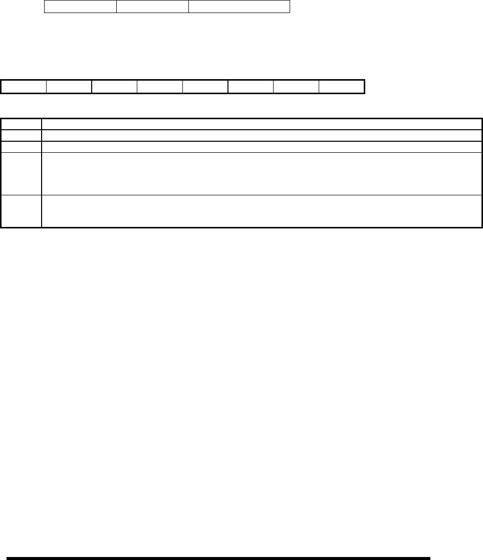
Toshiba Corporation Digital Media Network Company
Page 53 of 159
© 2004, Copyright TOSHIBA Corporation All Rights Reserved
11.7.7.2 SMART commands
This register should be set to C2h for SMART commands
11.7.8 Device/Head Register
- CS0 DA2-DA0 : 6 Read / Write
The value of this register is used to select the drive, Drive0 or Drive1, and head. On multiple sector
read/write operation that requires to cross track boundaries, the head select bit will be updated to reflect the
currently selected head number.
1 L 1 DEV HS3 HS2 HS1 HS0
Bit 7 Reserved (recommended to set 1)
Bit 6 L (Select LBA mode) L=0: CHS mode. L=1: LBA mode.
Bit 5 Reserved (recommended to set 1)
Bit 4 DEV (Device Select):
- (Drive0/Drive1 mode) This bit is used to select the drive. DEV= 0 indicates the first fixed disk drive
(Drive0), and DEV= 1 indicates the second (Drive1).
- (Single mode) should be 0. If this is 1, a drive is not selected but 00h shall be returned to status register.
Bit 3 -
Bit 0 HS3-HS0 (Head Select Bits) -- Bits 3 through 0 determine the required read/write head. Bit 0 is the
least-significant bit. If the L bit is equal to one (LBA Mode), the HS3 through HS0 bits contain bits 27
through 24 of the LBA.
Toshiba Corporation Digital Media Network Company
Page 54 of 159
© 2004, Copyright TOSHIBA Corporation All Rights Reserved
11.7.9 Status Register
-CS0 DA2-DA0:7 Read only
This register contains the command status. The contents of the register are updated at the completion of
each command and whenever the error occurs. The host system reads this register in order to acknowledge
the status and the result of each operation.
When the BSY bit (bit 7) is set, no other bits in the register are valid. And read/write operations of any other
register are negated in order to avoid the returning of the contents of this register instead of the other
resisters’ contents .
If the host reads this register when an interrupt is pending, interrupt request (INTRQ) is cleared in order to
work as Interrupt Acknowledge.
The bits of the status register are defined as below :
BSY DRDY DF DSC3 DRQ CORR IDX ERR
Bit 7 BSY (Busy) -- This bit is set when Host Reset (HRST) line is activated or Software Reset (SRST) bit in
Device Control register is set or when the COMMAND register is written and until a command is
completed but when Data Request is set to 1, this bit shall be reset. The host shouldn’t write or read any
registers when BSY = 1.
Bit 6 DRDY (Drive ready) -- DRDY=1 when seek complete bit (bit 4) = 1, indicates that the drive is ready to
respond read, write, or seek command. DRDY=0 indicates that read , write and seek are negated. A
command execution shall be interrupted if Not-Ready condition occurs during a command execution and
will be reset until the next command whether the drive condition is Ready or Not Ready. Error bit is set on
this occasion and will be reset just after power on and set again after the drive begins revolving at normal
speed and gets ready to receive a command.
Bit 5 DF (Device Fault) -- DF=1 indicates that the drive has detected a fault condition during the execution of a
Read Write commands; read, write, and seek commands are negated and Error bit is set. DF is set to 1
until the next command, whether the device is in fault condition or not.
Bit 4 DSC3 (Drive Seek Complete) – DSC³= 1 indicates that a seek operation has been completed. DSC³ is set
to 0 when a command accompanied by a seek operation begins. If a seek is not complete, a command is
terminated and this bit is not changed until the Status Register is read by the host . This bit remains reset
immediately after power on until the drive starts revolving at a nominal speed and gets ready to receive
command.
Bit 3 DRQ (Data Request) -- DRQ=1 indicates that the sector buffer requires 1 sector of data during a Read or
Write command.
Bit 2 CORR (Corrected Data) -- CORR=1 indicates that the data read from the disk had an error but was
successfully corrected by the read retry. This bit is always set to 0 and does not interrupt multi-sector
operations.
Bit 1 IDX (Index) -- This bit is a pulse signal set to 1 per revolution of the disk. Intervals of the signal may vary
during read / write operation. Therefore, the host shouldn’t use IDX for timing purposes.
Bit 0 ERR (Error) -- ERR = 1 indicates that an error occurred during execution of the previous command . The
cause of the error is reported on the other bit or in the error register. The error bit can be reset by the next
command from the controller. When this bit is set , a multi-sector operation is negated.
3 ATA-2 Notes: Prior to ATA-2 standard, this bit indicated that the device was on track. This bit may be used for other purposes in
future standards. For compatibility the drive supports this bit as ATA-1 specifies. User is recommended not to use this bit.

Toshiba Corporation Digital Media Network Company
Page 55 of 159
© 2004, Copyright TOSHIBA Corporation All Rights Reserved
11.7.10 Command Register
- CS0 DA2-DA0 : 7 Write only
The command register accepts commands for the drive to perform fixed disk operations. Commands are
executed when the TASK FILE is loaded and the command register is written and only when:
The status is not busy (BSY is inactive).
and
DRDY (drive ready) is active.
Any code NOT defined in the following list causes an Aborted Command error. Interrupt request (INTRQ)
is reset when a command is written. The following are acceptable commands to the command register.

Toshiba Corporation Digital Media Network Company
Page 56 of 159
© 2004, Copyright TOSHIBA Corporation All Rights Reserved
Table 11.7-2 Command Code
Command Code
Command Name Hex Value PARAMETERS USED
SC SN CY DRV HD FT
Nop 00H X X X O X X
Recalibrate 1xH X X X O X X
Read Sector(s) 20/21H O O O O O X
Read Sector(s) EXT 24h O O O O O X
Read DMA EXT 25H O O O O O X
Read Native Max Address EXT 27H X X X O X X
Read Multiple EXT 29H O O O O O X
Write Sector(s) 30/31H O O O O O X
Write Sector(s) EXT 34H O O O O O X
Write DMA EXT 35H O O O O O X
Set Max Address EXT 37H O O O O O X
Write Multiple EXT 39H O O O O O X
Write Verify 3CH O O O O O X
Read Verify Sector(s) 40/41H O O O O O X
Read Verify Sector(s) EXT 42H O O O O O X
Format Track 50H X X O O O X
Seek 7xH X X O O O X
Execute Diagnostics 90H X X X O X X
Initialize Device Parameters 91H O X X O O X
Download Microcode 92H O O X O X O
SMART B0H X X O O X O
Device Configuration B1H X X X O X O
Read Multiple C4H O O O O O X
Write Multiple C5H O O O O O X
Set Multiple Mode C6H O X X O X X
Read DMA C8/C9H O O O O O X
Write DMA CA/CBH O O O O O X
Power Control Stand-by Immediate E0 / 94H O X X O X X
Idle Immediate E1 / 95H O X X O X X
Stand-by E2 / 96H O X X O X X
Idle E3 / 97H O X X O X X
Check Power Mode E5 / 98H O X X O X X
Sleep E6 / 99H O X X O X X
Read Buffer E4H X X X O X X
Flush Cache E7H X X X O X X
Write Buffer E8H X X X O X X
Flush Cache EXT EAH X X X O X X
Identify Device ECH X X X O X X
Set Features EFH X X X O X O
Security Set Password F1H X X X O X X
Unlock F2H X X X O X X
Erase Prepare F3H X X X O X X
Erase Unit F4H X X X O X X
Freeze F5H X X X O X X
Disable Password F6H X X X O X X
Read Native Max Address F8H X X X O X X
Set Max F9H O O O O O X
Read Sence Data FCH X X X O X O
Note: O and X are defined as follows.
O = Must contain valid information for this command.
X = Don't care for this command.

Toshiba Corporation Digital Media Network Company
Page 57 of 159
© 2004, Copyright TOSHIBA Corporation All Rights Reserved
Parameters are defined as follows.
SC = SECTOR COUNT register.
SN = SECTOR NUMBER register.
CY = CYLINDER LOW and CYLINDER HIGH register.
DRV = DRIVE SELECT bit (bit 4 in DRIVE/HEAD register)
HD = HEAD SELECT bits (bit 3-0 in DRIVE/HEAD register)
FT = FEATURES register (WRITE PRECOMPENSATION register)
Toshiba Corporation Digital Media Network Company
Page 58 of 159
© 2004, Copyright TOSHIBA Corporation All Rights Reserved
11.7.11 Alternate Status Register
- CS1 DA2-DA0 : 6 Read only
This register contains the same information as the status register in the Task File. The only difference is that
this register being read does not imply interrupt acknowledge or doesn’t reset a pending interrupt.
See the description of status resister for definitions of the bit in this register.
11.7.12 Device Control Register
- CS1 DA2-DA0 : 6 Write only
This register contains the following three control bits.
HOB ---- ---- ---- 1 SRST - IEN ----
Bit 7 HOB (High Order Byte) is defined by the 48-bit Address feature set. A write to any Command register
shall clear the HOB bit to zero.
Bit 6-4 not used
Bit 3 Reserved (recommended to set 1)
Bit 2 SRST (Soft Reset) -- SRST= 1 indicates that the drive is held reset and sets BSY bit in Status register.
All internal registers are reset as shown in Table 11.12-1 . If two drives are daisy chained on the
interface, this bit will reset both drives simultaneously , regardless of the selection by Device address
bit in DEVICE/HEAD register.
Bit 1 - IEN (Interrupt Enable) -- When -IEN = 0, and the drive is selected by Drive select bit in
DEVICE/HEAD register, the drive interrupt to the host is enabled. When this bit is set, the - INTRQ
pin will be in a high impedance state, whether a pending interrupt is found or not.
Bit 0 not used
11.7.13 Device Address register4
- CS1 DA2-DA0 : 7 read only
The device address register is a read-only register used for diagnostic purposes. The followings are
definitions of bits for this register:
RSVD - WTG - HS3 - HS2 - HS1 - HS0 - DS1 - DS0
Bit 7 Reserved -- high impedance
Bit 6 - WTG (Write Gate) -- This bit is active when a Write to the disk is in progress.
Bit 5 - Bit 2 - HS3 to - HS0 (Head Select bits) -- Bit 5 through 2 are one's complement of the binary coded address of
currently selected head which is shown by Head Select bit in SDH register.
Bit 1 - DS1 (Drive Select 1) -- -DS1=0, when Drive1 is selected and active.
Bit 0 - DS0 (Drive Select 0) -- -DS0=0, when single mode or Drive0 in Drive0/Drive1 mode is selected and
active.
Note) The following facts should be taken into consideration when this resister is in use.
-WG reflects actual write gate in the drive, however, because of address transition or cache operation, there
is no direct connection with the data transferred between host and drive.
-HEAD SELECT represents one’s complement of the binary coded address of currently selected head, but
does not show actual selection of the head.
4 ATA-2 Notes: This register is obsolete. A device is not supposed to respond to a read of this address. If a device does
respond, it shall be sure not to drive the DD7 signal to prevent possible conflict with floppy disk implementations.
The drive supports this register to maintain compatibility for ATA-1.

Toshiba Corporation Digital Media Network Company
Page 59 of 159
© 2004, Copyright TOSHIBA Corporation All Rights Reserved
11.8 Command Descriptions
The drive interprets the commands written in the command register by the host system and executes them.
This table shows the drive’s response to the valid commands written in command-register.
Command Status register Error register
DRD
Y DF CORR ERR ICRC UNC IDNF ABRT TK0N
F AMNF
CHECK POWER MODE √ √ √ √
EXECUTE DEVICE DIAGNOSTIC √ √ √ See
Table 11.7-1
DEVICE CONFIGRATION RESTORE √ √ √ √
DEVICE CONFIGRATION FRESZE LOCK √ √ √ √
DEVICE CONFIGRATION IDENTIFY √ √ √ √
DEVICE CONFIGRATION SET √ √ √ √
DOWNLOAD MICROCODE √ √ √ √
FLUSH CACHE (EXT) √ √ √ √ √
FORMAT TRACK √ √ √ √ √ √ √ √
IDENTIFY DEVICE √ √ √ √
IDLE √ √ √ √
IDLE IMMEDIATE √ √ √ √
INITIALIZE DEVICE PARAMETERS √ √
READ BUFFER √ √ √ √
READ DMA (EXT) √ √ √ √ √ √ √ √
READ MULTIPLE (EXT) √ √ √ √ √ √ √
READ NATIVE MAX ADDRESS (EXT) √ √
READ SECTOR(S) (EXT) √ √ √ √ √ √ √
READ VERIFY SECTOR(S) (EXT) √ √ √ √ √ √ √
RECALIBRATE √ √ √ √ √
SECURITY DISABLE PASSWORD √ √ √ √ √
SECURITY ERASE PREPARE √ √ √ √ √
SECURITY ERASE UNIT √ √ √ √ √
SECURITY FREEZE LOCK √ √ √ √ √
SECURITY SET PASSWORD √ √ √ √ √
SECURITY UNLOCK √ √ √ √ √
SEEK √ √ √ √ √
SET FEATURES √ √ √ √
SET MAX ADDRESS (EXT) √ √ √ √
SET MAX SET PASSWORD √ √ √
SET MAX LOCK √ √ √
SET MAX UNLOCK √ √ √
SET MAX FLEEZE LOCK √ √ √
SET MULTIPLE MODE √ √ √ √
SLEEP √ √ √ √
SMART Enable/Disable Attribute autosave √ √ √ √
SMART Enable/Disable Automatic Off-line √ √ √ √
SMART DISABLE OPERATIONS √ √ √ √
SMART ENABLE OPERATIONS √ √ √ √
SMART RETURN STATUS √ √ √ √
SMART Read Attribute Values √ √ √ √ √ √
SMART Read Attribute Thresholds √ √ √ √
SMART Save Attribute Values √ √ √ √
SMART Execute OFF-LINE Immediate √ √ √ √ √
SMART Read Log Sector √ √ √ √ √ √
SMART Write Log Sector √ √ √ √ √
STANDBY √ √ √ √
STANDBY IMMEDIATE √ √ √ √
WRITE BUFFER √ √ √ √
WRITE DMA (EXT) √ √ √ √ √ √
WRITE MULTIPLE (EXT) √ √ √ √ √
WRITE SECTOR(S) (EXT) √ √ √ √ √
WRITE VERIFY √ √ √ √ √
Invalid command code √ √ √ √
√ = valid on this command

Toshiba Corporation Digital Media Network Company
Page 60 of 159
© 2004, Copyright TOSHIBA Corporation All Rights Reserved
11.8.1 Nop (00h)
COMMAND CODE 0 0 0 0 0 0 0 0 REGISTER
REGISTER SETTING NORMAL COMPLETION
DR drive no. no change
CY no change
HD no change
SN no change
SC no change
FT no change
LBA no change
The Nop command reports the status. The drive terminates the command with aborted error after receiving
this command.
11.8.2 Recalibrate5 (1xh)
COMMAND CODE 0 0 0 1 X X X X REGISTER
REGISTER SETTING NORMAL COMPLETION
DR drive no. no change
CY 00H
HD no change
SN no change
SC no change
FT no change
LBA 00H
This command will set BSY bit and move the R/W heads on the disk to cylinder 0. At the completion of a
seek , it revises the status, resets BSY and generates an interrupt.
11.8.3 Flush Cache (E7h)
COMMAND CODE 1 1 1 0 0 1 1 1
RESISTER SETTING DR drive no.
This command reports the completion of a Write cache to the host. At the completion of a Write cache,
the drive revises the status, resets BSY and generates an interrupt.
11.8.4 Flush Cache EXT (EAh)
COMMAND CODE 1 1 1 0 1 0 1 0
RESISTER SETTING DR drive no.
This command reports the completion of a Write cache to the host. At the completion of a Write cache,
the drive revises the status, resets BSY and generates an interrupt.
5 ATA/ATAPI-4 defines this command as Vendor specific. The drive supports this command to maintain ATA-3, and the previous
models compatibility. User is recommended not to use this command.
Toshiba Corporation Digital Media Network Company
Page 61 of 159
© 2004, Copyright TOSHIBA Corporation All Rights Reserved
11.8.5 Read Sector (20h/21h)
COMMAND CODE 0 0 1 0 0 0 0 X REGISTER
REGISTER SETTING NORMAL COMPLETION
DR drive no. no change
CY starting cylinder last possible
HD starting head last possible
SN starting sector last possible
SC no. of sector to read 00H
FT no change
LBA staring address last address
Setting BSY bit, the drive will seek to the target cylinder if the head is not on target track ( implied seek ), select
the head and begin to read the number of sector defined in SC register ( 1-256 ) starting from the target sector.
After finding ID of target sector and having 1 sector of data read into the buffer RAM, the drive sets DRQ in
status register and generates interrupt to report to the host that the drive is ready to transfer the next data.
In case of multi-sector transfer, DRQ bit is reset and BSY is set after 1 sector transfer to prepare for the next
sector transfer.
An uncorrectable data can also be transferred but the subsequent operation will terminate at the cylinder, head,
and sector (or LBA) position in the TASK FILE register. When a sector is ready to be read by the host, an
interrupt is issued. After the last sector is read by the host, no interrupt is issued at the end of a command.
11.8.6 Read Sector EXT (24h)
COMMAND CODE 0 0 1 0 0 1 0 0 REGISTER
REGISTER SETTING NORMAL COMPLETION
DR drive no. no change
LBA
Low Current
Previous LBA(7:0)
LBA(31:24) HOB=0
HOB=1 last address
last address
LBA
Mid Current
Previous LBA(15:8)
LBA(39:32) HOB=0
HOB=1 last address
last address
LBA
High Current
Previous LBA(23:16)
LBA(47:40) HOB=0
HOB=1 last address
last address
SC Current
Previous sector count(7:0)
sector count(15:8) HOB=0
HOB=1 00H
00H
FT Current
Previous reserved
reserved HOB=0
HOB=1 no change
no change
Setting BSY bit, the drive will seek to the target cylinder if the head is not on target track ( implied seek ), select
the head and begin to read the number of sector defined in SC register ( 1-65536 ) starting from the target
sector. After finding ID of target sector and having 1 sector of data read into the buffer RAM, the drive sets DRQ
in status register and generates interrupt to report to the host that the drive is ready to transfer the next data.
In case of multi-sector transfer, DRQ bit is reset and BSY is set after 1 sector transfer to prepare for the next
sector transfer.
An uncorrectable data can also be transferred but the subsequent operation will terminate at the LBA position
in the TASK FILE register. When a sector is ready to be read by the host, an interrupt is issued. After the last
sector is read by the host, no interrupt is issued at the end of a command.
This command is available in LBA addressing only.
Toshiba Corporation Digital Media Network Company
Page 62 of 159
© 2004, Copyright TOSHIBA Corporation All Rights Reserved
11.8.7 Write Sector (30h/31h)
COMMAND CODE 0 0 1 1 0 0 0 X REGISTER
REGISTER SETTING NORMAL COMPLETION
DR drive no. no change
CY starting cylinder last possible
HD starting head last possible
SN starting sector start sector
SC no. of sector to write 00H
FT no change
LBA starting address last possible
The drive seeks to the target cylinder and selects the head and begins to write to the number of sectors
defined in SC register (1-256) starting from the target sector. DRQ in status register is set as soon as the
command register is written and the buffer RAM receives the data transferred from the host . After 1 sector
is transferred to the buffer RAM, the drive resets DRQ, sets BSY and begins write operation. In case of
multi-sector transfer, it sets DRQ bit, resets BSY and generates Interrupt to inform host that it is ready to
transfer the next 1 sector of data. The drive will seek to the target cylinder if the head is not on the target
track (implied seek). After transferring the last data in the buffer, it resets BSY and issues an interrupt.
If an error occurs during multi-sector transfer, it will terminate the transfer by setting error information in
status register and error register, without shifting into data transfer mode from the host. CY, HD, SN ( LBA)
registers show the address where error has occurred.
11.8.8 Write Sector EXT (34h)
COMMAND CODE 0 0 1 1 0 1 0 0 REGISTER
REGISTER SETTING NORMAL COMPLETION
DR drive no. no change
LBA
Low Current
Previous LBA(7:0)
LBA(31:24) HOB=0
HOB=1 last address
last address
LBA
Mid Current
Previous LBA(15:8)
LBA(39:32) HOB=0
HOB=1 last address
last address
LBA
High Current
Previous LBA(23:16)
LBA(47:40) HOB=0
HOB=1 last address
last address
SC Current
Previous sector count(7:0)
sector count(15:8) HOB=0
HOB=1 00H
00H
FT Current
Previous reserved
reserved HOB=0
HOB=1 no change
no change
The drive seeks to the target cylinder and selects the head and begins to write to the number of sectors
defined in SC register (1-65536) starting from the target sector. DRQ in status register is set as soon as
the command register is written and the buffer RAM receives the data transferred from the host . After 1
sector is transferred to the buffer RAM, the drive resets DRQ, sets BSY and begins write operation. In
case of multi-sector transfer, it sets DRQ bit, resets BSY and generates Interrupt to inform host that it is
ready to transfer the next 1 sector of data. The drive will seek to the target cylinder if the head is not on the
target track (implied seek). After transferring the last data in the buffer, it resets BSY and issues an
interrupt.
If an error occurs during multi-sector transfer, it will terminate the transfer by setting error information in
status register and error register, without shifting into data transfer mode from the host. LBA registers show
the address where error has occurred.
This command is available in LBA addressing only.
Toshiba Corporation Digital Media Network Company
Page 63 of 159
© 2004, Copyright TOSHIBA Corporation All Rights Reserved
11.8.9 Read Verify (40h)
COMMAND CODE 0 1 0 0 0 0 0 0 REGISTER
REGISTER SETTING NORMAL COMPLETION
DR drive no. no change
CY starting cylinder last possible
HD starting head last possible
SN starting sector start sector
SC no. of sector to be read 00H
LBA starting address last address
This command is identical to a Read command except that the drive has read the data from the media, and
the DRQ bit is not set and no data is sent to the host. This allows the system to verify the integrity of the
drive. A single interrupt is generated upon completion of a command or when an error occurs.
11.8.10 Read Verify EXT (42h)
COMMAND CODE 0 1 0 0 0 0 1 0 REGISTER
REGISTER SETTING NORMAL COMPLETION
DR drive no. no change
LBA
Low Current
Previous LBA(7:0)
LBA(31:24) HOB=0
HOB=1 last address
last address
LBA
Mid Current
Previous LBA(15:8)
LBA(39:32) HOB=0
HOB=1 last address
last address
LBA
High Current
Previous LBA(23:16)
LBA(47:40) HOB=0
HOB=1 last address
last address
SC Current
Previous sector count(7:0)
sector count(15:8) HOB=0
HOB=1 00H
00H
FT Current
Previous reserved
reserved HOB=0
HOB=1 no change
no change
This command is identical to a Read EXT command except that the drive has read the data from the media,
and the DRQ bit is not set and no data is sent to the host. This allows the system to verify the integrity of
the drive. A single interrupt is generated upon completion of a command or when an error occurs.
This command is available in LBA addressing only.
11.8.11 Write Verify6 (3Ch)
6 ATA/ATAPI-4 defines this command as Vendor specific. The drive supports this command to maintain ATA-3 compatibility. User is
recommended not to use this command.
Toshiba Corporation Digital Media Network Company
Page 64 of 159
© 2004, Copyright TOSHIBA Corporation All Rights Reserved
COMMAND CODE 0 0 1 1 1 1 0 0 REGISTER
REGISTER SETTING NORMAL COMPLETION
DR drive no. no change
CY starting cylinder last possible
HD starting head last possible
SN starting sector start sector
SC no. of sector to be written 00H
LBA starting address last address
This command is all identical to a Write sector command. Read verification is not performed in this
command. A Write verify command transfers the number of sectors (1-256) defined in SC register from the
host to the drive, then the data is written on the media. The starting sector is defined in CY, HD, SN (LBA)
registers.
Upon receipt of the command, the drive sets DRQ until one sector of data is transferred from the host, then
resets DRQ, sets BSY. In case of multi- sector transfer, it sets DRQ, resets BSY and generate an interrupt
to report the host that the host is ready to receive 1 sector of data. The drive will seek to the target track if
the R/W head is not on the target track (implied seek). Reaching the target sector, the command transfers
the sector data from the host to the media. After transferring the last data in the buffer, it sets BSY and
issues an Interrupt.
11.8.12 Format Track 7 (50h)
COMMAND CODE 0 1 0 1 0 0 0 0 REGISTER
REGISTER SETTING NORMAL COMPLETION
DR drive no. no change
CY cylinder to format no change
HD head to format no change
SN 01H
SC 00H
FT no change
The track specified by the task file is formatted with ID and data fields according to the table transferred to
the buffer. This command is rejected in LBA mode with an Aborted command error reported.
DRQ in status register is set as soon as the command register is written, and the buffer RAM receives the
data transferred from the host. After 512 bytes are transferred into the buffer RAM, the drive resets DRQ,
sets BSY and begins format operation. The drive seeks to the target cylinder if the head is not on the target
track ( implied seek ). After completion of the command, it resets BSY and generates an interrupt.
Format table consists of the number of sectors ( 16 bits ) per track . Upper byte represents sector number,
and lower byte represents format type.
The drive supports only 00H format type. Intending to maintain compatibility with previous models, the drive
accepts any format type, but the function will not change.
Sector interleave is always set to one regardless of sector sequence in the format table. Data subsequent
to format table are handled as “Don't care”.
7 ATA/ATAPI-4 defines this command as Vendor specific. The drive supports this command to maintain ATA-3, and the previous
models compatibility. User is recommended not to use this command.

Toshiba Corporation Digital Media Network Company
Page 65 of 159
© 2004, Copyright TOSHIBA Corporation All Rights Reserved
FORMAT TABLE ( FIRST 86 BYTES )
(Ex. 43 logical sector mode)
0001, 0002, 0003, 0004, 0005, 0006, 0007, 0008, 0009, 0013, 0015, 0016, 0017, 0018,.0019,
001A,.......0029, 002A, 002B
DON’T CARE ( 426 BYTES ATTACHED )
0000, 0000, 0000, 0000, 0000, 0000, 0000, 0000, 0000, 0000, 0000, 0000, 0000, ........... 0000, 0000, 0000.
Toshiba Corporation Digital Media Network Company
Page 66 of 159
© 2004, Copyright TOSHIBA Corporation All Rights Reserved
11.8.13 Seek (7xh)
COMMAND CODE 0 1 1 1 X X X X REGISTER
REGISTER SETTING NORMAL COMPLETION
DR drive no. no change
CY cylinder to seek no change
HD head to seek no change
SN no change
SC no change
FT no change
LBA address to seek no change
This command moves the R/W heads to the cylinder specified in the task files. The drive sets BSY and
starts seek operation. After the completion of a seek operation, the drive asserts DSC8 , negates BSY ,
and return the interrupt.
If CY, HD and SN registers show invalid address, “ID Not Found” error is reported and no seek operation
shall be executed. All commands related to data access possess Implied Seek function and don't need this
command.
11.8.14 Toshiba Specific
COMMAND CODE 1 0 0 0 X X X X
1 0 0 1 1 0 1 0
1 1 1 1 0 0 0 0
1 1 1 1 0 1 1 1
1 1 1 1 1 0 1 X
1 1 1 1 1 1 X X
These commands are only for factory use. Host must not issue them.
11.8.15 Execute Diagnostics (90h)
COMMAND CODE 1 0 0 1 0 0 0 0 REGISTER
REGISTER SETTING NORMAL COMPLETION
DR OOH
CY OOH
HD OOH
SN O1H
SC O1H
FT
This command enables the drive to execute following self-test and reports the results to the error register
described in Table 10.7.2-1.
(1) ROM checksum test
(2) RAM test
(3) Controller LSI register test
An interrupt is generated at the completion of this command.
When two drives are daisy-chained on the interface, both drives execute the self test and the Drive0 reports
valid error information of the two drives.
8 ATA-2 Notes: Prior to ATA-2 standard, this bit indicated that the device was on track. This bit may be used for other purposes in
future standards. For compatibility the drive supports this bit as ATA-1 specifies. User is recommended not to use this bit.

Toshiba Corporation Digital Media Network Company
Page 67 of 159
© 2004, Copyright TOSHIBA Corporation All Rights Reserved
11.8.16 Initialize Device Parameters (91h)
COMMAND CODE 1 0 0 1 0 0 0 1 REGISTER
REGISTER SETTING NORMAL COMPLETION
DR drive number no change
CY no change
HD total number of heads-1 no change
SN number of sector per track no change
SC no change
FT no change
This command specifies the number of sectors per track and the number of heads per cylinder to set head
switching point and cylinder increment point. Specified values affect Number of the current logical heads,
Number of logical sectors per track, which can be read by Identify Device Command.
On issuing this command, the content of CY register shall not be checked. This command will be terminated
with ABORT error when it is issued on a invalid HD or SC register setting ( SC register=0 or the combination
of HD and SC register exceeds the drive parameter.
Any drive access command should accompany correct HD, SN register with heads and sectors within the
number specified for this command. Otherwise, it results in “ID not found” error. If the number of heads
and drives is within the specified number, command gives parameter to convert an address to access into
Logical Block Address (LBA). ID Not Founderror also occur when this LBA exceeds the total number of
user addressable sectors. The command does not affect LBA address mode.

Toshiba Corporation Digital Media Network Company
Page 68 of 159
© 2004, Copyright TOSHIBA Corporation All Rights Reserved
11.8.17 Download Microcode (92h)
COMMAND CODE 1 0 0 0 0 0 1 0 REGISTER
REGISTER SETTING NORMAL COMPLETION
DR drive number no change
CY 00h
HD no change
SN number of sector(high order) 00h
SC number of sector(low order) 00h
FT subcommand code no change
This command enables the host to alter the device’s microcode. The data transferred using the
DOWNLOAD MICROCODE command is vendor specific.
All transfers shall be an integer multiple of the sector size. The size of the data transfer is determined by the
contents of the Sector Number register and the Sector Count register. The Sector Number register shall be
used to extend the Sector Count register to create a 16-bit sector count value. The Sector Number register
shall be the most significant eight bits and the Sector Count register shall be the least significant eight bits.
A value of zero in both the Sector Number register and the Sector Count register shall specify no data is to
be transferred.This allows transfer sizes from 0 bytes to 33,553,920 bytes, in 512 byte increments.
The Features register shall be used to determine the effect of the DOWNLOAD MICROCODE command.
The values for the Features register are:
− 07h - save downloaded code for immediate and future use.
This feature(07h) is supported. All other values are reserved.

Toshiba Corporation Digital Media Network Company
Page 69 of 159
© 2004, Copyright TOSHIBA Corporation All Rights Reserved
11.8.18 Read Multiple (C4h)
COMMAND CODE 1 1 0 0 0 1 0 0 REGISTER
REGISTER SETTING NORMAL COMPLETION
DR drive number no change
CY starting cylinder last possible
HD starting head last possible
SN starting sector last possible
SC number of sector to read 00H
FT no change
LBA starting address last possible
The read multiple command performs similarly to the Read Sectors command except for the following
features. Interrupts are not issued on each sector, but on the transfer of each block which contains the
number of sectors defined by a Set Multiple Mode command or the default , if no intervening Set Multiple
command has been issued.
Command execution is identical to the Read Sectors operation except that the number of sectors defined by
a Set Multiple Mode command are transferred without interrupts. DRQ qualification of the transfer is required
only at the start of a data block transfer, not required for the transfer of each sector.
The block count of sectors to be transferred without intervening interrupts is programmed by the Set Multiple
Mode command, which shall be executed prior to the Read Multiple command.
When the Read Multiple command is issued, the Sector Count Register contains the number of required
sectors ( not the number of blocks or the block count ) . If the number of required sectors is not evenly
divisible by the block count, The redundant sectors are transferred during the final partial block transfer. The
partial block transfer shall be for N sectors, where
N = The redundant sector count ( block count )
If the Read Multiple command is attempted when Read Multiple command are disabled, the Read Multiple
operation shall be rejected with an Aborted Command error.
Disk errors occurred during Read Multiple command are posted at the beginning of the block or partial block
transfer, but DRQ is still set and the data, including corrupted data, shall be transferred as they normally
would .
The contents of the Command Block Registers following the transfer of a data block which has a sector in
error are undefined. The host should retry the transfer as individual requests to obtain valid error
information.
Subsequent blocks or defective blocks are transferred only when the error is a correctable data error. All
other errors after the transfer of the block containing the error terminates the command . Interrupts are
generated when DRQ is set at the beginning of each block or partial block.
Toshiba Corporation Digital Media Network Company
Page 70 of 159
© 2004, Copyright TOSHIBA Corporation All Rights Reserved
11.8.19 Read Multiple EXT (29h)
COMMAND CODE 0 0 1 0 1 0 0 1 REGISTER
REGISTER SETTING NORMAL COMPLETION
DR drive no. no change
LBA
Low Current
Previous LBA(7:0)
LBA(31:24) HOB=0
HOB=1 last address
last address
LBA
Mid Current
Previous LBA(15:8)
LBA(39:32) HOB=0
HOB=1 last address
last address
LBA
High Current
Previous LBA(23:16)
LBA(47:40) HOB=0
HOB=1 last address
last address
SC Current
Previous sector count(7:0)
sector count(15:8) HOB=0
HOB=1 00H
00H
FT Current
Previous reserved
reserved HOB=0
HOB=1 no change
no change
This command is basically identical to Read Multiple command except register setting.
This command is available in LBA addressing only.
11.8.20 Write Multiple (C5h)
COMMAND CODE 1 1 0 0 0 1 0 1 REGISTER
REGISTER SETTING NORMAL COMPLETION
DR drive number no change
CY starting cylinder last possible
HD starting head last possible
SN starting sector start sector
SC number of sector to write 00H
FT no change
LBA starting address last possible
This command performs similarly to the Write Sectors command except for the following features. The Drive
sets BSY immediately upon receipt of the command, and interrupts are not issued on each sector but on
the transfer of each block which contains the number of sectors defined by Set Multiple Mode command or
the default if no intervening Set Multiple command has been issued.
Command execution is identical to the Write Sectors operation except that no interrupt is generated during
the transfer of number of sectors defined by the Set Multiple Mode command but generated for each block.
DRQ qualification of the transfer is required only for each data block, not for each sector.
The block count of sectors to be transferred without programming of intervening interrupts by the Set
Multiple Mode command, which shall be executed prior to the Write Multiple command.
When the Write Multiple command is issued, the host sets the number of sectors ( not the number of blocks
or the block count ) it requests in the Sector Count Register. If the number of required sectors is not evenly
divisible by the block count, the redundant sectors are transferred during the final partial block transfer. The
partial block transfer shall be for N sectors, where
N = The redundant sector count ( block count )
If the Write Multiple command is attempted when Write Multiple command are disabled, the Write Multiple
operation shall be rejected with an Aborted Command error.

Toshiba Corporation Digital Media Network Company
Page 71 of 159
© 2004, Copyright TOSHIBA Corporation All Rights Reserved
Disk errors occurred during Write Multiple command are posted after the attempted disk write of the block or
partial block which are transferred. The Write Multiple command is terminated at the sector in error , even if
it was in the middle of a block. Subsequent blocks are not transferred after an error. Interrupts are generated
for each block or each sector, when DRQ is set .
After the transfer of a data block which contains a sector with error, the contents of the Command Block
Registers are undefined. The host should retry the transfer as individual requests to obtain valid error
information.
Toshiba Corporation Digital Media Network Company
Page 72 of 159
© 2004, Copyright TOSHIBA Corporation All Rights Reserved
11.8.21 Write Multiple EXT (39h)
COMMAND CODE 0 0 1 1 1 0 0 1 REGISTER
REGISTER SETTING NORMAL COMPLETION
DR drive no. no change
LBA
Low Current
Previous LBA(7:0)
LBA(31:24) HOB=0
HOB=1 last address
last address
LBA
Mid Current
Previous LBA(15:8)
LBA(39:32) HOB=0
HOB=1 last address
last address
LBA
High Current
Previous LBA(23:16)
LBA(47:40) HOB=0
HOB=1 last address
last address
SC Current
Previous sector count(7:0)
sector count(15:8) HOB=0
HOB=1 00H
00H
FT Current
Previous reserved
reserved HOB=0
HOB=1 no change
no change
This command is basically identical to Write Multiple command except register setting.
This command is available in LBA addressing only.
11.8.22 Set Multiple Mode (C6h)
COMMAND CODE 1 1 0 0 0 1 1 0 REGISTER
REGISTER SETTING NORMAL COMPLETION
DR drive no. no change
CY no change
HD no change
SN no change
SC The number of sectors / block no change
FT no change
This command enables the drive to perform Read and Write Multiple operations and sets the block count for
these commands.
The Sector Count Register is loaded with the number of sectors per block. The drive supports 1,2,4,8 or16
sectors per block.
Upon receipt of the command, the drive sets BSY=1 and checks the content of Sector Count Register.
If the Sector Count Register contains a valid value and the block count is supported, the value is loaded for
all subsequent Read Multiple and Write Multiple commands. And these commands are enabled to be
executed. If a block count is not supported , this command shall be terminated with the report of an Aborted
Command error , and Read Multiple and Write Multiple commands are disabled.
If the Sector Count Register contains 0 when the command is issued, Read Multiple and Write Multiple
commands are disabled.
In case of software reset, the result depends on the setting of Set Feature command. If FT=66h, the mode
is not changed. If FT = CCh, the mode reverts to power on default (16 sectors).
Toshiba Corporation Digital Media Network Company
Page 73 of 159
© 2004, Copyright TOSHIBA Corporation All Rights Reserved
11.8.23 Read DMA (C8h/C9h)
COMMAND CODE 1 1 0 0 1 0 0 X REGISTER
REGISTER SETTING NORMAL COMPLETION
DR drive no. no change
CY starting cylinder last possible
HD starting head last possible
SN starting sector last possible
SC no. of sector to read 00H
FT no change
LBA staring address last address
This command is basically identical to Sector command except following features.
• Host initialize the DMA channel before issuing command.
- Data transfer is initiated by DMARQ and handled by the DMA channel in the host.
- Drive issues only one interrupt at the completion of each command to show the status is valid after data
transfer.
During DMA transfer phase, either BSY or DRQ is set to 1.
When a command is completed, CY, HD, SN register (LBA register) shows the sector transferred the latest.
If the drive detects unrecoverable error, the drive terminate the command and CY, HD, SN register (LBA
register) shows the sector where error occurred.
11.8.24 Read DMA EXT (25h)
COMMAND CODE 0 0 1 0 0 1 0 1 REGISTER
REGISTER SETTING NORMAL COMPLETION
DR drive no. no change
LBA
Low Current
Previous LBA(7:0)
LBA(31:24) HOB=0
HOB=1 last address
last address
LBA
Mid Current
Previous LBA(15:8)
LBA(39:32) HOB=0
HOB=1 last address
last address
LBA
High Current
Previous LBA(23:16)
LBA(47:40) HOB=0
HOB=1 last address
last address
SC Current
Previous sector count(7:0)
sector count(15:8) HOB=0
HOB=1 00H
00H
FT Current
Previous reserved
reserved HOB=0
HOB=1 no change
no change
This command is basically identical to Read DMA command except register setting.
This command is available in LBA addressing only.
Toshiba Corporation Digital Media Network Company
Page 74 of 159
© 2004, Copyright TOSHIBA Corporation All Rights Reserved
11.8.25 Write DMA (CAh/CBh)
COMMAND CODE 1 1 0 0 1 0 1 X REGISTER
REGISTER SETTING NORMAL COMPLETION
DR drive no. no change
CY starting cylinder last possible
HD starting head last possible
SN starting sector last possible
SC no. of sector to write 00H
FT no change
LBA staring address last address
This command is basically identical to Sector command except following differences.
• Host initialize the DMA channel before issuing command.
- Data transfer is initiated by DMARQ and handled by the DMA channel in the host.
- Drive issue only one interrupt at the completion of each command to show the status is valid after data
transfer.
During DMA transfer phase, either BSY or DRQ is set to 1.
When a command is completed, CY, HD, SN register (LBA register) shows the sector transferred the latest.
If the drive detects unrecoverable error, the drive terminates the command and CY, HD, SN register (LBA
register) shows the sector where error has occurred.
11.8.26 Write DMA EXT (35h)
COMMAND CODE 0 0 1 1 0 1 0 1 REGISTER
REGISTER SETTING NORMAL COMPLETION
DR drive no. no change
LBA
Low Current
Previous LBA(7:0)
LBA(31:24) HOB=0
HOB=1 last address
last address
LBA
Mid Current
Previous LBA(15:8)
LBA(39:32) HOB=0
HOB=1 last address
last address
LBA
High Current
Previous LBA(23:16)
LBA(47:40) HOB=0
HOB=1 last address
last address
SC Current
Previous sector count(7:0)
sector count(15:8) HOB=0
HOB=1 00H
00H
FT Current
Previous reserved
reserved HOB=0
HOB=1 no change
no change
This command is basically identical to Write DMA command except register setting.
This command is available in LBA addressing only.

Toshiba Corporation Digital Media Network Company
Page 75 of 159
© 2004, Copyright TOSHIBA Corporation All Rights Reserved
11.8.27 Power Control (Exh)
COMMAND CODE 1 1 1 0 X X X X REGISTER
REGISTER SETTING NORMAL COMPLETION
DR drive no. no change
CY no change
HD no change
SN no change
SC shown below 00/FFH (for E5/98 command)
no change (for other command)
FT no change
Power Control is a group of commands which controls low power mode in the drive. The drive has three
types of power mode:
Idle, Stand-by and Sleep mode
At the completion of disk access, the drive automatically enters the idle mode.
There are two ways to shift to the stand-by mode ( to stop rotation of spindle motor ).
By a command from the host
By internal timer
The internal timer is set by Stand-by or Idle command. If the drive receives disk access command from the
host when it is in stand-by mode , the spindle starts rotating and the drive executes read/write operation.
After power on, the spindle starts rotating and enters the idle mode. During idle or stand-by, READY bit is
set and the drive is ready to receive a command.
To be specific , there are four different sub-commands defined by lower 4 bits of command as follows. The
drive is in the idle mode when it is in default condition after power- on.
11.8.27.1 Stand-by Immediate (E0/94)
SC=X (Don't care)
The drive enters the stand-by mode immediately by this command. If the drive is already in the stand-by
mode, it does no-operation and the stand-by timer doesn’t start .The drive issues an interrupt and reports
the host that the command has been completed before it virtually enters the stand-by mode .
11.8.27.2 Idle Immediate (E1/95)
SC=X
The drive enters the idle mode immediately by this command. If the drive is already in the idle mode, it
does no-operation. If stand-by timer is enabled, timer will start. After the drive enters the idle mode, the
drive issues interrupt to report the host that the command has been completed.
Toshiba Corporation Digital Media Network Company
Page 76 of 159
© 2004, Copyright TOSHIBA Corporation All Rights Reserved
11.8.27.3 Stand-by (E2/96)
This command causes the device to enter stand-by mode.
If SC is non-zero then stand-by timer shall be enabled. The value in SC shall be used to determine the time
programmed into the stand-by timer.
If SC is zero then the stand-by timer is disabled.
Value in SC register Setting
0 Time out disabled
1-240 (SC x 5) sec.
241-251 ((value - 240) x 30) min.
252 21 min
253 Period between 8 and 12 hrs
254 Reserved
255 21 min 15 sec.
When the specified time period has passed, the drive enters stand-by mode. If a disk access command is
received during stand-by mode, the spindle starts rotating and the drive executes read/write operation.
After completing the command, the drive reset stand-by timer and the timer starts counting down.
11.8.27.4 Idle (E3/97)
This command causes the device to enter idle mode.
If SC is non-zero then stand-by timer shall be enabled. The value in SC shall be used to determine the time
programmed into the stand-by timer.
If SC is zero then the stand-by timer is disabled.
Value in SC register Setting
0 Time out disabled
1-240 (SC x 5) sec.
241-251 ((value - 240) x 30) min.
252 21 min
253 Period between 8 and 12 hrs
254 Reserved
255 21 min 15 sec.
When the specified time period has expired, the drive enters the stand-by mode. If disk access command
is received during the stand-by mode, the spindle starts rotating and executes read/write operation. After
completing the command, The drive resets stand-by timer and the timer starts counting down.
11.8.27.5 Check Power Mode (E5/98)
SC result value=00 indicates that the drive is in stand-by mode or going into stand-by mode or is shifting
from stand-by mode into idle mode.
SC result value=FFH indicates that the drive is in idle mode.
11.8.27.6 Sleep (E6/99)
When SC=X, the drive enters sleep mode immediately. After entering the sleep mode, the drive issues an
interrupt to report the host that the command has been completed. The drive recovers from sleep mode and
enters stand-by mode by receiving a reset.
Toshiba Corporation Digital Media Network Company
Page 77 of 159
© 2004, Copyright TOSHIBA Corporation All Rights Reserved
11.8.28 Read Buffer (E4h)
COMMAND CODE 1 1 1 0 0 1 0 0 REGISTER
REGISTER SETTING NORMAL COMPLETION
DR drive no. no change
CY no change
HD no change
SN no change
SC 00H
FT no change
This command transfers a specified sector of data ( 512 bytes) from the 128kB buffer in the drive to the host.
When this command is issued, the drive sets BSY, sets up the buffer for read operation, sets DRQ, resets
BSY, and generates an interrupt. The host reads up to 512 bytes of data from the buffer.
11.8.29 Write Buffer (E8h)
COMMAND CODE 1 1 1 0 1 0 0 0 REGISTER
REGISTER SETTING NORMAL COMPLETION
DR drive no. no change
CY no change
HD no change
SN no change
SC 00H
FT no change
This command transfers a sector of data from the host to the specified 512 bytes of 128kB buffer of the
drive . When this command is issued, the drive will set up the buffer for write operation, and set DRQ. The
host may then write up to 512 bytes of data to the buffer.

Toshiba Corporation Digital Media Network Company
Page 78 of 159
© 2004, Copyright TOSHIBA Corporation All Rights Reserved
11.8.30 Identify Device (ECh)
COMMAND CODE 1 1 1 0 1 1 0 0 REGISTER
REGISTER SETTING NORMAL COMPLETION
DR drive no. no change
CY no change
HD no change
SN no change
SC 00H
FT no change
The identify device command requests the drive to transfer parameter information to the host. When the
command is issued, the drive sets BSY, stores the required parameter information in the sector buffer, sets
the DRQ bit, and issues an interrupt. The host may read the parameter information of the sector buffer.
The parameter words in the buffer are arranged as shown in Table 11.8-1 ~ Table 11.8-5.

Toshiba Corporation Digital Media Network Company
Page 79 of 159
© 2004, Copyright TOSHIBA Corporation All Rights Reserved
Table 11.8-1 Identify Information
WORD DESCRIPTION Hex.
0 General configuration
15 0=ATA device
14-8 Reserved
7 1=Removable cartridge device
6 1=Fixed device
5-3 Reserved
2 Response incomplete
1-0 Reserved
0040
1 Number of default logical cylinders [1*]
2 Specific configuration C837
3 Number of default logical heads [2*]
4 Reserved 0000
5 Reserved 0000
6 Number of default logical sectors h logical track [3*]
7-9 Reserved
10-19 Serial Number (20 ASCII characters)
20 Reserved 0000
21 Reserved 0000
22 Reserved 0000
23-26 Firmware Revision (8 ASCII characters)
27-46 Controller model # (40 ASCII characters)
47 15-8 80h
7-0 00H = READ/WRITE MULTIPLE command not implemented
01H- FFH = Maximum number of sectors that can be transferred per
interrupt on READ/WRITE MULTIPLE commands
8010
48 Reserved 0000
49 Capabilities
15-14 Reserved
13 1=Standby timer values as specified in ATA/ATAPI-6 specification are
supported
0=Standby timer values are vendor specific
12 Reserved
11 1=IORDY supported
10 1=IORDY can be disabled
9 1=LBA supported
8 1=DMA supported
7-0 Reserved
2F00
50 Capabilities
15 0 (Fixed)
14 1 (Fixed)
13-1 Reserved
0 1= a device specific Standby timer value minimum.
4000
51 15-8 PIO data transfer cycle timing mode
7-0 Reserved 0200
52 Reserved 0000
53 15-3 Reserved
2 1=the fields reported word 88 are valid
0=the fields reported word 88 are not valid
1 1=the fields reported words 64-70 are valid
0=the fields reported words 64-70 are not valid
0 1=the fields reported words 54-58 are valid
0=the fields reported words 54-58 are not valid
0007
54 Number of current cylinders XXXX
55 Number of current heads XXXX
56 Number of current sectors per track XXXX

Toshiba Corporation Digital Media Network Company
Page 80 of 159
© 2004, Copyright TOSHIBA Corporation All Rights Reserved
Table 11.8-2 Identify Information (Continued)
WORD DESCRIPTION Hex.
57-58 Current capacity in sectors
(Number of current cylinders * Number of current heads * Number of current
sectors per track)
XXXX
59 15-9 Reserved
8 1=Multiple sector setting is valid
7-0 XXh=Current setting for number of sectors that can be transferred per
interrupt on R/W Multiple command
01XX
60-61 Total number of user addressable sectors (LBA mode only) [5*]
62 15-0 Reserved XX07
63 15-8 Multiword DMA transfer mode active
7-0 Multiword DMA transfer mode supported XX07
64 15-8 reserved
7-0 Advanced PIO Transfer Modes Supported
bit 7-2 Reserved
bit 1 = 1 PIO MODE 4 supported
bit 0 = 1 PIO MODE 3 supported
0003
65 Minimum Multiword DMA Transfer Cycle Time Per Word (ns) 0078
66 Manufacturer’s Recommended Multiword DMA Transfer Cycle Time 0078
67 Minimum PIO Transfer Cycle Time Without Flow Control (ns) 0078
68 Minimum PIO Transfer Cycle Time With IOCHRDY Flow Control 0078
69-79 Reserved (for future command overlap and queuing) 0000
80 Major version number
0000h or FFFFh = device does not report version
15-7 Reserved for ATA-7~14
6 1=supports ATA/ATAPI-6
5 1=supports ATA/ATAPI-5
4 1=supports ATA/ATAPI-4
3 1=supports ATA-3
2 1=supports ATA-2
1 1=supports ATA-1
0 Reserved
007E
81 Minor version number
0000h or FFFFh = device does not report version 0000
82 Command set supported.
0000h or FFFFh = command set notification not supported
15 Reserved
14 1=NOP command supported
13 1=READ BUFFER command supported
12 1=WRITE BUFFER command supported
11 Reserved
10 1=Host Protected Area feature set supported
9 1=DEVICE RESET command supported
8 1=SERVICE interrupt supported
7 1=release interrupt supported
6 1=look-ahead supported
5 1=write cache supported
4 1=supports PACKET Command feature set
3 1=supports power management feature set
2 1=supports removable feature set
1 1=supports security feature set
0 1=supports SMART feature set
746B

Toshiba Corporation Digital Media Network Company
Page 81 of 159
© 2004, Copyright TOSHIBA Corporation All Rights Reserved
Table 11.8-3 Identify Information (Continued)
WORD DESCRIPTION Hex.
83 Command set supported.
0000h or FFFFh = command set notification not supported
15 0 (Fixed)
14 1(Fixed)
13 1=FLUSH CACHE EXT command supported
12 1=FLUSH CACHE command supported
11 1=Device Configuration Overlay supported
10 1=48-bit Address feature set supported
9 1=Automatic Acoustic Management feature set supported
8 1=Set MAX security extension supported
7 Reserved
6 1=SET FEATURES subcommand required to spin up after power-up
5 1=Power-Up in Standby feature set supported
4 1=Removable Media Status Notification feature set supported
3 1=Advanced Power Management feature set supported
2 1=CFA feature set supported
1 1=READ / WRITE DMA QUEUED supported
0 1=DOWNLOAD MICROCODE command supported
7D09
84 Command set/feature supported extension
15 0 (Fixed)
14 1(Fixed)
13 1(Fixed)
12-6 Reserved
5 1=General Purpose Logging feature set supported
4 1=Reserved
3 1=Media Card Pass Through Command feature set supported
2 1=Media serial number supported
1 1=SMART self-test supported
0 1=SMART error logging supported
6023
85 Command set/feature enabled
15 Reserved
14 1=NOP command enabled
13 1=READ BUFFER command enabled
12 1=WRITE BUFFER command enabled
11 Reserved
10 1=Host Protected Area feature set enabled
9 1=DEVICE RESET command enabled
8 1=SERVICE interrupt enabled
7 1=release interrupt enabled
6 1=look -ahead enabled
5 1=write cache enabled
4 1=PACKET Command feature set supported
3 1=power management feature set enabled
2 1=removable feature set enabled
1 1=Security feature set enabled
0 1=SMART feature enabled
XXXX
86 Command set/feature enabled
15-14 Reserved
13 1=FLUSH CACHE EXT command supported
12 1=FLUSH CACHE command supported
11 1=Device Configuration Overlay supported
10 1=48-bit Address feature set supported
9 1=Automatic Acoustic Management feature set enabled
8 1=SET MAX security extension enabled by SET MAX SET
PASSWORD
7 Reserved
6 1=SET FEATURES subcommand required to spin-up after power-up
5 1=Power-Up In Standby feature set enabled
4 1=Removable Media Status Notification feature set enabled
3 1=Advanced Power Management feature set enabled
2 1=CFA feature set enabled
1 1=READ / WRITE DMA QUEUED supported
0 1=DOWNLOAD MICROCODE command supported
XX0X

Toshiba Corporation Digital Media Network Company
Page 82 of 159
© 2004, Copyright TOSHIBA Corporation All Rights Reserved
Table 11.8-4 Identify Information (Continued)
WORD DESCRIPTION Hex.
87 Command set/feature default
15 0 (Fixed)
14 1 (Fixed)
13 1 (Fixed)
12-6 Reserved
5 1=General Purpose Logging feature set supported
4 Reserved
3 1=Media Card Pass Through Command feature set enabled
2 1=Madia serial number is valid
1 1=SMART self-test supported
6023
88 15-8 Ultra DMA transfer mode selected
7-0 Ultra DMA transfer modes supported XX3F
89 Time required for security erase unit completion 00XX
90 Time required for Enhanced Security erase completion 0000
91 Current Advanced Power Management setting
15-8 Reserved
7-0 Current Advanced Power Management setting set by Set Features
Command
00XX
92 Master Password Revision Code XXXX
93 Hardware reset result. The conetnts of bits 12-0 of this word shall change only
during the execution of a hardware reset.
15 0 (Fixed)
14 1 (Fixed)
13 1=device detected CBLID- above VIH
0=device detected CBLID- below VIL
12-8 Device 1 hardware reset result. Device 0 shall clear these bits to
zero.
Device 1 shall set these bits as follows :
12 Reserved.
11 0=Device 1 did not assert PDIAG-.
1=Device 1 asserted PDIAG-.
10-9 These bits indicate how Device 1 determined the device
number:
00=Reserved.
01=a jumper was used.
10=the CSEL signal was used.
11=some other method was used or the method is
unknown.
8 1 (Fixed)
7-0 Device 0 hardware reset result. Device 1 shall clear these bit to
zero.
Device 0 shall set these bills as follows:
7 Reserved.
6 0=Device 0 does not respond when Device 1 is selected.
1=Device 0 responds when Device 1 is selected.
5 0=Device 0 did not detect the assertion of DASP-.
1=Device 0 detected the assertion of DASP-.
4 0=Device 0 did not detect the assertion of PDIAG-.
1=Device 0 detected the assertion of PDIAG-.
3 0=Device 0 failed diagnostics.
1=Device 0 passed diagnostics.
2-1 These bits indicate how Device 0 determined the device
number:
00=Reserved.
01=a jumper was used.
10=the CSEL signa was used.
11=some other method was used or the method is
unknown.
0 1 (Fixed)
XXXX
94 Current automatic acoustic management value
15-8 Vendor’s recommended acoustic management value
7-0 Current automatic acoustic management value
0000
95-99 Reserved 0000
100-103 Maximum user LBA for 48-bit Address feature set XXXX
104-126 Reserved 0000

Toshiba Corporation Digital Media Network Company
Page 83 of 159
© 2004, Copyright TOSHIBA Corporation All Rights Reserved
Table 11.8-5 Identify Information (Continued)
WORD DESCRIPTION Hex.
127 Removable Media Status Notification feature set supported
15-2 Reserved
1-0 00=Removable Media Status Notification feature set not supported
01=Removable Media Status Notification feature set supported
10=Reserved
11=Reserved
0000
128 Security status
15-9 Reserved
8 Security level 0=High, 1=Maximum
7-6 Reserved
5 1=Enhanced security erase supported
4 1=Security count expired
3 1=Security frozen
2 1=Security locked
1 1=Security enabled
0 1=Security supported
0XXX
129-159 Reserved 0000
160 CFA power mode 1
15 Word 160 supported
14 Reserved
13 CFA power mode 1 is required for one or more commands
implemented by the device
12 CFA power mode 1 disabled
11-0 Maximum current in ma
0000
161-175 Reserved 0000
176-205 Current media serial number 0000
206-254 Reserved 0000
255 Integrity word
15-8 Checksum
7-0 Signature
XXA5
Toshiba Corporation Digital Media Network Company
Page 84 of 159
© 2004, Copyright TOSHIBA Corporation All Rights Reserved
Word descriptions:
WORD 0: General configuration
bit 15 0=ATA
bit 14-8 Reserved
bit 7 1=Removable cartridge
bit 6 1=Fixed disk drive
bit 5-3 Reserved
bit 2 Response incomplete
bit 1-0 Reserved
The value for this WORD is 0040h.
WORD 1: Logical cylinder number that user can access (in default mode) [*1]
WORD 2: Specific configuration
“37C8” : Device requires SET FEATURES subcommand to spin-up after power-up and IDENTIFY DEVICE
response is incomplete.
“738C” : Device requires SET FEATURES subcommand to spin-up after power-up and IDENTIFY DEVICE
response is complete.
“8C73” : Device does not requires SET FEATURES subcommand to spin-up after power-up and IDENTIFY
DEVICE response is incomplete.
“C837” : Device does not requires SET FEATURES subcommand to spin-up after power-up and IDENTIFY
DEVICE response is complete.
“All other valies” : Reserved
Power-up in Standby feature set is not supported.
The value for this WORD is C837h.
WORD 3: Logical head number that user can access (in default mode) [*2]
WORD 4-5: Reserved
WORD 6: The number of logical sector per track (in default mode) [*3]
Default Values : [*1],[*2],[*3]
Drive Type [*1] : Word 1 [*2] : Word 3 [*3] : Word 6
MK1032GAX 16383 16 63
WORD 7-9: Reserved
WORD 10-19: Serial number
WORD 20-21: Reserved
WORD 22: Reserved

Toshiba Corporation Digital Media Network Company
Page 85 of 159
© 2004, Copyright TOSHIBA Corporation All Rights Reserved
WORD 23-26: Firmware revision ( 8 ASCII characters )
WORD 27-46: Model name (40 ASCII characters)
Drive Type
MK1032GAX TOSHIBA_MK1032GAX_..._
“_” indicates ASCII space code.
WORD 47:
bit 15 - 8 shall be set to 80h
bit 7 - 0 Maximum number of sectors that can be transferred per interrupt on READ/WRITE MULTIPLE
commands.
The default value for this WORD is 8010h.
WORD 48: Reserved
WORD 49: Capabilities
bit 15-14 0=Reserved
bit 13 1=Standby timer value shall be as specified in ATA-/ ATAPI-6 specification
0=Standby timer value are vendor specific
bit 12 Reserved (For advanced PIO mode support)
bit 11 1=IORDY is supported.
bit 10 1=IORDY function can be disabled.
bit 9 1=LBA supported
bit 8 1=DMA supported
bit 7- 0 Reserved
The value for this WORD is 2F00h.
WORD 50: Capabilities
bit 15 0 (Fixed)
bit 14 1 (Fixed)
bit 13-1 Reserved
bit 0 1=device has a minimum Standby timer value that is device specific.
Standby timer value is set to 5 minutes or more. The value for this WORD is 4000h.
WORD 51: PIO data transfer cycle timing mode
bit 15- 8 PIO data transfer cycle timing mode
bit 7- 0 Reserved
The value returned in Bits 15-8 should fall into one of the mode 0 through mode.
Note: For backwards compatibility with BIOS written before Word 64 was defined for advanced modes, a
device reports in Word 51 the highest original PIO mode (i.e. PIO mode 0, 1, or 2) it can support.
The value for this WORD is 0200h.
WORD 52: Reserved
WORD 53:
bit15- 3 Reserved
bit 2 1= the fields reported in word 88 is valid
bit 1 1= the fields reported in words 64∼70 are valid
bit 0 1= the fields reported in words 54∼58 are valid
If the number of heads and sectors exceed the drive parameter, bit 0 and related WORD 54-58 shall be
cleared to 0. The default value for this WORD is 0007h.
Toshiba Corporation Digital Media Network Company
Page 86 of 159
© 2004, Copyright TOSHIBA Corporation All Rights Reserved
WORD 54: Number of current cylinders defined by INITIALIZE DEVICE PARAMETERS command
WORD 55: Number of current heads defined by INITIALIZE DEVICE PARAMETERS command
WORD 56: Number of current sectors/track defined by INITIALIZE DEVICE PARAMETERS command
WORD 57-58: Total number of sectors calculated by word 54 - 56
bit31-24 by word 58 bit 7- 0
bit23-16 by word 58 bit 15- 8
bit15- 8 by word 57 bit 7- 0
bit 7- 0 by word 57 bit 15- 8
The power on values for each models are.
Drive Type [*4] :」 Word 57 - 58
MK1032GAX 16,514,064(FBFC10H)
WORD 59:
bit15- 9 Reserved
bit 8 1=bit 7- 0 shows number of sectors for multiple sector operation (multiple sector operation is
enabled by SET MULTIPLE command).
bit 7∼0 The number of sectors transferred for XXH =Write / Read multiple command with 1 Interrupt
( Current value shall be set by SET MULTIPLE command. The default value is 16 ).
The default value for this WORD is 0110h.
WORD 60-61: Maximum number of sectors that user can access in LBA mode
bit31-24 by word 61 bit 7- 0
bit23-16 by word 61 bit 15- 8
bit15- 8 by word 60 bit 7- 0
bit 7- 0 by word 60 bit 15- 8
The maximum value that shall be placed in this field is 0FFFFFFFh.
The power on values for each models are.
Drive Type [*5] : Word 60 – 61
MK1032GAX 195,371,568 (BA52230H)

Toshiba Corporation Digital Media Network Company
Page 87 of 159
© 2004, Copyright TOSHIBA Corporation All Rights Reserved
WORD 62: Reserved
WORD 63: Mode information for multiword DMA
bit15- 8 Active mode
bit 10 1=Mode 2 is active
bit 9 1=Mode 1 is active
bit 8 1=Mode 0 is active
bit 7- 0 Supported mode
bit 2 1=mode 2 is supported
bit 1 1=mode 1 is supported
bit 0 1=mode 0 is supported
Support bit reflects setting by SET FEATURE command.
The default value for this WORD is 0407h and the default figure is mode 2
WORD 64: Mode information for Advanced PIO transfer
bit 7- 0 Supported mode
bit 1 1=mode 4 is supported
bit 0 1=mode 3 is supported
The value for this WORD is 0003h.
WORD 65: Minimum multiword DMA transfer mode cycle time per word (ns)
If this bit is supported, word 53 bit 1 shall be set. The value for this WORD is 0078h (120ns).
WORD 66: Manufacturer recommended multiword DMA transfer cycle time
If the data transfer is requested in a shorter cycle time than this definition, the data transfer may be kept
pending with DMARQ low because data is not ready. The value for this WORD is 0078h (120ns).
WORD 67: Minimum PIO transfer cycle time without flow control (ns)
The Drive can guarantee correct data transfer without flow control in this cycle time or longer. If this bit is
supported, word 53 bit 1 is to be set. The drives which support PIO mode 3 or higher shall support this field
too. This figure shall not be less than 120. The value for this WORD is 0078h (120ns).
WORD 68: Minimum PIO transfer cycle time with IORDY flow control (ns)
If this bit is supported, word 53 bit 1 is to be set. The drive that support PIO mode 3 or higher shall support
this field too. This figure shall not be less than 120. The value for this WORD is 0078h (120ns).

Toshiba Corporation Digital Media Network Company
Page 88 of 159
© 2004, Copyright TOSHIBA Corporation All Rights Reserved
WORD 69-79: Reserved
WORD 80: Major version number
If not 0000h or FFFFh, the device claims compliance with the major version(s) as indicated by bits 1 - 6
being equal to one. Values other than 0000h and FFFFh are bit significant. Since the ATA standards
maintain downward compatibility, a device may set more than one bit .
WORD 81: Minor version number
If an implementor claims that the revision of the standard they used to guide their implementation does not
need to be reported or if the implementation was based upon a standard prior to this revision of the
standard, Word 81 shall be 0000h or FFFFh.
WORD 82: Command sets supported
bit 15 Reserved
bit 14 NOP command supported
bit 13 READ BUFFER command supported
bit 12 WRITE BUFFER command supported
bit 11 Reserved
bit 10 Host Protected Area feature set supported
bit 9 DEVICE RESET command supported
bit 8 SERVICE interrupt supported
bit 7 Release Interrupt supported
bit 6 Look Ahead supported
bit 5 Write Cache supported
bit 4 PACKET feature set supported
bit 3 The Power Management feature set is supported
bit 2 The Removable feature set is supported
bit 1 The security feature set is supported
bit 0 The SMART feature set is supported
The value for this WORD is 746Bh.
WORD 83: Features/Command sets supported
bit 15 0 (Fixed)
bit 14 1 (Fixed)
bit 13 1=FLUSH CACHE EXT command supported
bit 12 1=FLUSH CACHE command supported
bit 11 1=Device Configuration Overlay supported
bit 10 1=48-bit Address feature set supported
bit 9 1=Automatic Acoustic Management feature set supported
bit 8 1=Set MAX security extension supported
bit 7 Reserved
bit 6 1=SET FEATURES subcommand required to spin up after power-up
bit 5 1=Power-Up in Standby feature set supported
bit 4 1=Removable Media Status Notification feature set supported
bit 3 Advanced Power Management feature set supported
bit 2 1=CFA feature set supported
bit 1 1=READ / WRITE DMA QUEUED supported
bit 0 1=DOWNLOAD MICROCODE command supported
The value for this WORD is 7D09h.

Toshiba Corporation Digital Media Network Company
Page 89 of 159
© 2004, Copyright TOSHIBA Corporation All Rights Reserved
WORD 84: Features / Command sets supported
bit 15 0 (Fixed)
bit 14 1 (Fixed)
bit 13 1 (Fixed)
bit 12-6 Reserved
bit 5 1=General Purpose Logging feature set supported
bit 4 Reserved
bit 3 1=Media Card Pass Through command feature set supported
bit 2 1=Media serial number supported
bit 1 1=SMART self-test supported
bit 0 1=SMART error logging supported
The value for this WORD is 6023h.
WORD 85: Features / Command sets enable
bit 15 Reserved
bit 14 NOP command enabled
bit 13 READ BUFFER command enabled
bit 12 WRITE BUFFER command enabled
bit 11 Reserved
bit 10 Host Protected Area feature set enabled
bit 9 DEVICE RESET command enabled
bit 8 SERVICE interrupt enabled
bit 7 Release Interrupt enabled
bit 6 Look Ahead enabled
bit 5 Write Cache enabled
bit 4 PACKET feature set supported
bit 3 The Power Management feature set is enabled
bit 2 The Removable feature set is enabled
bit 1 The security feature set is enabled
bit 0 The SMART feature set is enabled
The default value for this WORD is 7468h
WORD 86: Features / Command sets enabled
bit 15-14 Reserved
bit 13 1=FLUCH CACHE EXT command supported
bit 12 1=FLUSH CACHE command supported
bit 11 1=Device Configuration Overlay supported
bit10 1=48-bit Address feature set supported
bit 9 1=Automatic Acoustic Management feature set enabled
bit 8 1=SET MAX security extension enabled by SET MAX SET PASSWORD
bit 7 Reserved
bit 6 1=SET FEATURES subcommand required to spin-up after power-up
bit 5 1=Power-Up In Standby feature set enabled
bit 4 Removable Media Status Notification feature set enabled
bit 3 Advanced power Management feature set enabled
bit 2 CFA feature set enabled
bit 1 WRITE / READ DMA QUEUED command supported
bit 0 DOWNLOAD MICROCODE supported
The default value for this WORD is 3C09h.
Toshiba Corporation Digital Media Network Company
Page 90 of 159
© 2004, Copyright TOSHIBA Corporation All Rights Reserved
WORD 87: Features / Command sets enabled
bit 15 0 (Fixed)
bit 14 1 (Fixed)
bit 13 1 (Fixed)
bit 12-6 Reserved
bit 5 1=General Purpose Logging feature set supported
bit 4 Reserved
bit 3 1=Media Card Pass Through command feature set enabled
bit 2 1=Media serial number is valid
bit 1 1=SMART self-test supported
bit 0 1=SMART error logging supported
The value for this WORD is 6023h.
WORD 88: Mode information for Ultra DMA
The active mode reflects the command change.
bit 15-8 Active transfer mode
bit 13 1=Mode 5 is active
bit 12 1=Mode 4 is active
bit 11 1=Mode 3 is active
bit 10 1=Mode 2 is active
bit 9 1=Mode 1 is active
bit 8 1=Mode 0 is active
bit 7-0 Supported mode
bit 5 1=Mode 5 is supported
bit 4 1=Mode 4 is supported
bit 3 1=Mode 3 is supported
bit 2 1=Mode 2 is supported
bit 1 1=Mode 1 is supported
bit 0 1=Mode 0 is supported
The default value for this WORD is 003Fh
WORD 89: The time period for Security Erase Unit command completion shall be set.
TIMER
A
CTUAL VALUE
0 Not s
p
ecified
1-254
(
Timer ×2
)
minuites
255 > 508 minuites
WORD 90: Time required for Enhanced Security erase completion
WORD 91: Current Advanced Power Management setting
bit 15-8 Reserved
bit 7-0 Current Advanced Power Management setting set by Set Features Command.
The default value for this WORD is0080h.
WORD 92: Master Password Revision Code
the value of the Master Password Revision Code set when the Master Password was last change. Valid
values are 0001h through FFFEh. A value of 0000h or FFFFh indicates that the Master Password
Revision is not supported.

Toshiba Corporation Digital Media Network Company
Page 91 of 159
© 2004, Copyright TOSHIBA Corporation All Rights Reserved
WORD 93: Hardware configuration test results
bit 15 0 (Fixed)
bit 14 1 (Fixed)
bit 13 1=device detected CBLID- above VIH
0=device detected CBLID- below VIL
bit12-8 Device 1 hardware reset result. Device 0 shall clear these bits to zero.
Device 1 shall set these bits as follows :
12 Reserved.
11 0=Device 1 did not assert PDIAG-.
1=Device 1 asserted PDIAG-.
10-9 These bits indicate how Device 1 determined the device number:
00=Reserved.
01=a jumper was used.
10=the CSEL signal was used.
11=some other method was used or the method is unknown.
8 1 (Fixed)
bit 7-0 Device 0 hardware reset result. Device 1 shall clear these bit to zero.
Device 0 shall set these bills as follows:
7 Reserved.
6 0=Device 0 does not respond when Device 1 is selected.
1=Device 0 responds when Device 1 is selected.
5 0=Device 0 did not detect the assertion of DASP-.
1=Device 0 detected the assertion of DASP-.
4 0=Device 0 did not detect the assertion of PDIAG-.
1=Device 0 detected the assertion of PDIAG-.
3 0=Device 0 failed diagnostics.
1=Device 0 passed diagnostics.
2-1 These bits indicate how Device 0 determined the device number:
00=Reserved.
01=a jumper was used.
10=the CSEL signa was used.
11=some other method was used or the method is unknown.
0 1 (Fixed)
WORD 94: Current automatic acoustic management value
bit 15-8 Vendor’s recommended acoustic management value
bit 7-0 Current automatic acoustic management value
This function is not supported. The value for this WORD is 0000h.
WORD 95-99: Reserved
WORD 100-103: Maximum User LBA for 48-bit Address feature set
The value for this WORD is XXXXh.
WORD 104-126: Reserved
WORD 127: Removable Media Status Notification feature set supported
This function is not supported. The value for this WORD is 0000h.

Toshiba Corporation Digital Media Network Company
Page 92 of 159
© 2004, Copyright TOSHIBA Corporation All Rights Reserved
WORD 128: Security status
bit 15-9 Reserved
bit 8 the security level.
1=the security level is maximum
0=the security level is high
bit 5 1=the Enhanced security erase unit feature supported
bit 4 the security count has expired.
1=the security count is expired and SECURITY UNLOCK and SECURITY ERASE UNIT are aborted
until receiving a power-on reset or hard reset.
bit 3 security frozen.
1=the drive is in security frozen mode.
bit 2 security locked.
1=the drive is in security locked mode.
bit 1 security enabled.
1=the security is enabled.
bit 0 security supported.
1=security is supported.
WORD 129-159: Reserved
WORD 160: CFA power mode
bit 15 Word 160 supported
bit 14 Reserved
bit 13 CFA power mode 1 is required for one or more commands implemented by the device
bit 12 CFA power mode 1 disabled
bit 11-0 Maximum current in ma
This function is not supported. The value for this WORD is 0000h.
WORD 161-175: Reserved
WORD 176-205: Current media serial number
This function is not supported. The value for this WORD is 0000h.
WORD 206-254: Reserved
WORD 255: Integrity word
The data structure checksum is the two s complement of the sum of all bytes in words 0 through 254 and
the byte consisting of bits 7:0 in word 255. Each byte shall be added with unsigned arismetic, and overflow
shall be ignored. The sum of all 512 bytes is zero when the checksum is correct.
Toshiba Corporation Digital Media Network Company
Page 93 of 159
© 2004, Copyright TOSHIBA Corporation All Rights Reserved
11.8.31 SET MAX (F9h)
Individual SET MAX commands are identified by the value placed in the Features register. Table 11.8-6 shows
these Features register values. But regardless of Feature register value, the case this command is immediately
proceded by a Read Native Max ADRESS comamnd, it is interpreted as a Set Max ADDRESS command.
Table 11.8-6 SET MAX Features register values
Value Command
00h Obsolete
01h SET MAX SET PASSWORD
02h SET MAX LOCK
03h SET MAX UNLOCK
04h SET MAX FREEZE LOCK
05h-FFh Reserved
11.8.31.1 Set Max Address
COMMAND CODE 1 1 1 1 1 0 0 1 REGISTER
REGISTER SETTING NORMAL COMPLETION
DR DRIVE No. no change
CY Max. cylinder number no change
HD Max. head number no change
SN Max. sector number no change
SC 00H / 01 H (BITO: reserved bit) no change
FT no change
LBA Max. LBA no change
This command specifies the the maximum address in a range of actual drive capacity. The values set in CY,
HD, SN registers indicate the maximum address that can be accessed. In CHS mode, the value of Read Native
Max Address command should be set in HD, SN register. Otherwise, the value shall be ignored and the value of
Read Max Address command will be used. If an LBA bit (DRV / HD register bit 6) is set, the value in LBA mode
shall be set. If the address exceeding the set value is accessed , “ ABORT ERROR “ error will be reported. This
set value affects the values of WORD 1, 54, 57, 58, 60, 61, 100-103 of IDENTIFY DEVICE command.
This command shall be immediately preceded by Read Native Max Address command. Otherwise, it will be
terminated with “ ABORT ERROR ” .
If this command is issued twice with a volatile bit set to 1 after power-up or hardware reset, “ID Not Found
error” will be reported.
If a host protected area has been established by a SET MAX ADDRESS EXT command, this command will be
terminated with “ ABORT ERROR ” .
Volatile bit ( SC register bit 0 ) :
If this command is issued with a volatile bit set to 1, the set value of this command is valid after power-up or
hardware reset.
If this command is issued with a volatile bit cleared to 0, the set value of this command shall be cleared after
hard reset or power-on and the maximam value shall be the last value with a volatile bit set to 1.
Toshiba Corporation Digital Media Network Company
Page 94 of 159
© 2004, Copyright TOSHIBA Corporation All Rights Reserved
11.8.31.2 Set Max Set Password
F9h with the content of the Features register equal to 01h.
COMMAND CODE 1 1 1 1 1 0 0 1 REGISTER
REGISTER SETTING NORMAL COMPLETION
DR DRIVE No. no change
CY no change
HD no change
SN no change
SC no change
FT 01 H no change
LBA no change
This command is not immediately preceded by a READ NATIVE MAX ADDRESS command. If this command is
immediately preceded by a READ NATIVE MAX ADDRESS command, it shall be interpreted as a SET MAX
ADDRESS command.
This command requests a transfer of a single sector of data from the host. Table 11.8-7 defines the content of
this sector of information. The password is retained by the device until the next power cycle. When the device
accepts this command the device is in Set_Max_Unlocked state.
Table 11.8-7 SET MAX SET PASSWORD data content
Word Content
0 Reserved
1-16 Password (32 bytes)
17-255 Reserved
11.8.31.3 Set Max Lock
F9h with the content of the Features register equal to 02h.
COMMAND CODE 1 1 1 1 1 0 0 1 REGISTER
REGISTER SETTING NORMAL COMPLETION
DR DRIVE No. no change
CY no change
HD no change
SN no change
SC no change
FT 02 H no change
LBA no change
This command is not immediately preceded by a READ NATIVE MAX ADDRESS command. If this command is
immediately preceded by a READ NATIVE MAX ADDRESS command, it shall be interpreted as a SET MAX
ADDRESS command.
The SET MAX LOCK command sets the device into Set_Max_Locked state. After this command is completed
any other SET MAX commands except SET MAX UNLOCK and SET MAX FREEZE LOCK are rejected. The
Toshiba Corporation Digital Media Network Company
Page 95 of 159
© 2004, Copyright TOSHIBA Corporation All Rights Reserved
device remains in this state until a power cycle or the acceptance of a SET MAX UNLOCK or SET MAX
FREEZE LOCK command.
11.8.31.4 Set Max Unlock
F9h with the content of the Features register equal to 03h.
COMMAND CODE 1 1 1 1 1 0 0 1 REGISTER
REGISTER SETTING NORMAL COMPLETION
DR DRIVE No. no change
CY no change
HD no change
SN no change
SC no change
FT 03 H no change
LBA no change
This command is not immediately preceded by a READ NATIVE MAX ADDRESS command. If this command is
immediately preceded by a READ NATIVE MAX ADDRESS command, it shall be interpreted as a SET MAX
ADDRESS command.
This command requests a transfer of a single sector of data from the hostTable 11.8-7 defines the content of this
sector of information.
The password supplied in the sector of data transferred shall be compared with the stored SET MAX password.
If the password compare fails, then the device returns command aborted and decrements the unlock counter.
On the acceptance of the SET MAX LOCK command, this counter is set to a value of five and shall be
decremented for each password mismatch when SET MAX UNLOCK is issued and the device is locked. When
this counter reaches zero, then the SET MAX UNLOCK command shall return command aborted until a power
cycle.
If the password compare matches, then the device shall make a transition to the Set_Max_Unlocked state and
all SET MAX commands shall be accepted.
11.8.31.5 Set Max Freeze Lock
F9h with the content of the Features register equal to 04h
COMMAND CODE 1 1 1 1 1 0 0 1 REGISTER
REGISTER SETTING NORMAL COMPLETION
DR DRIVE No. no change
CY no change
HD no change
SN no change
SC no change
FT 04 H no change
LBA no change

Toshiba Corporation Digital Media Network Company
Page 96 of 159
© 2004, Copyright TOSHIBA Corporation All Rights Reserved
A SET MAX SET PASSWORD command shall previously have been successfully completed. This command is
not immediately preceded by a READ NATIVE MAX ADDRESS command. If this command is immediately
preceded by a READ NATIVE MAX ADDRESS command, it is interpreted as a SET MAX ADDRESS command.
The SET MAX FREEZE LOCK command sets the device to Set_Max_Frozen state. After command completion
any subsequent SET MAX commands are rejected.
Commands disabled by SET MAX FREEZE LOCK are:
− SET MAX ADDRESS
− SET MAX SET PASSWORD
− SET MAX LOCK
− SET MAX UNLOCK
11.8.32 SET MAX ADDRESS EXT (37h)
COMMAND CODE 0 0 1 1 0 1 1 1 REGISTER
REGISTER SETTING NORMAL COMPLETION
DR drive no. no change
LBA
Low Current
Previous Max LBA(7:0)
Max LBA(31:24) HOB=0
HOB=1 no change
no change
LBA
Mid Current
Previous Max LBA(15:8)
Max LBA(39:32) HOB=0
HOB=1 no change
no change
LBA
High Current
Previous Max LBA(23:16)
Max LBA(47:40) HOB=0
HOB=1 no change
no change
SC Current
Previous 00H / 01 H
reserved HOB=0
HOB=1 no change
no change
FT Current
Previous reserved
reserved HOB=0
HOB=1 no change
no change
This command specifies the the maximum address in a range of actual drive capacity. If the address exceeding
the set value is accessed , “ ABORT ERROR “ error will be reported. This set value affects the values of WORD
60, 61, 100-103 of IDENTIFY DEVICE command.
This command shall be immediately preceded by Read Native Max Address EXT command. Otherwise, it will
be terminated with “ ABORT ERROR ” .
If this command is issued twice with a volatile bit set to 1 after power-up or hardware reset, “ID Not Found
error” will be reported.
If a host protected area has been established by a SET MAX ADDRESS command, this command will be
terminated with “ ABORT ERROR ” .
Volatile bit ( SC register bit 0 ) :
If this command is issued with a volatile bit set to 1, the set value of this command is valid after power-up or
hardware reset.
If this command is issued with a volatile bit cleared to 0, the set value of this command shall be cleared after
hard reset or power-on and the maximam value shall be the last value with a volatile bit set to 1.
Toshiba Corporation Digital Media Network Company
Page 97 of 159
© 2004, Copyright TOSHIBA Corporation All Rights Reserved
11.8.33 Read Native Max Address (F8h)
COMMAND CODE 1 1 1 1 1 0 0 0 REGISTER
REGISTER SETTING NORMAL COMPLETION
DR DRIVE No. no change
CY maximum cylinder number
HD maximum head number
SN maximum sector number
LBA maximum LBA
This command sets the maximum address in CY, HD, SN register. If LBA ( DRV / HD register bit6 ) is set to 1,
the maximum address shall be LBA value.
If the 48-bit native max address is greater than 268,435,455, the Read Native Max Address command shall
return a maximum value of 268,435,454.
11.8.34 Read Native Max Address EXT (27h)
COMMAND CODE 0 0 1 0 0 1 1 1 REGISTER
REGISTER SETTING NORMAL COMPLETION
DR drive no. no change
LBA
Low Current
Previous HOB=0
HOB=1 Max LBA(7:0)
Max LBA(31:24)
LBA
Mid Current
Previous HOB=0
HOB=1 Max LBA(15:8)
Max LBA(39:32)
LBA
High Current
Previous HOB=0
HOB=1 Max LBA(23:16)
Max LBA(47:40)
SC Current
Previous HOB=0
HOB=1 no change
no change
FT Current
Previous reserved
reserved HOB=0
HOB=1 no change
no change
This command sets the maximum address (LBA value).
Toshiba Corporation Digital Media Network Company
Page 98 of 159
© 2004, Copyright TOSHIBA Corporation All Rights Reserved
11.8.35 Set Features (EFh)
COMMAND CODE 1 1 1 0 1 1 1 1 REGISTER
REGISTER SETTING NORMAL COMPLETION
DR DRIVE No. no change
CY no change
HD no change
SN no change
SC Mode Selection for Data Transfer(*2) no change
FT Features(*1) no change
(*1) Features: FT register defines following selections.
02H Enable write cache feature
03H Select data transfer mode
05H Enable advanced power management
55H Disable read look-ahead feature
66H Disable reverting to power on defaults by soft reset
82H Disable write cache feature
85H Disable advanced power management
AAH Enable read look-ahead feature
CCH Enable reverting to power on defaults by soft reset
others Invalid (reporting with Aborted Command Error)
(*2)Mode selection for data transfer is specified in sector count register. Upper 5 bits show transfer mode
and lower 3 bits show mode figure.
PIO default transfer mode 00000 000
PIO default transfer mode, disable IORDY 00000 001
PIO flow control transfer mode nnn 00001 nnn
Multiword DMA mode nnn 00100 nnn
Ultra DMA mode nnn 01000 nnn
Reserved 10000 nnn
PIO default mode is mode 4 flow control. DMA default mode is Multiword DMA mode 2.
The level of Advanced Power Management function is set in Sector count register.
C0h-FEh …… Mode0 (Power save up to Low Power Idle)
80h-BFh …… Mode1 (Power save up to Low Power Idle)
01h-7Fh …… Mode2 (Power save up to Standby)
00h,FFh …… Aborted
Transition time of power save is changed dynamically in Mode1 and Mode2 due to Adaptive power control
function. The function level is set to Mode1 when Advanced Power Management function is disabled.
If FT register has any other value, the drive rejects the command with Abort Command error.
Default settings after power on or hard reset are:
Data transfer mode of Multiword DMA mode 2, PIO mode 4 flow control,
4 bytes ECC, look-ahead read enabled, write cache enabled, advanced power management enabled,
READ/WRITE Multiple command enabled (16 sectors)
and reverting to power on defaults by soft reset disabled.
Toshiba Corporation Digital Media Network Company
Page 99 of 159
© 2004, Copyright TOSHIBA Corporation All Rights Reserved
11.8.36 SECURITY SET PASSWORD (F1h)
COMMAND CODE 1 1 1 1 0 0 0 1 REGISTER
REGISTER SETTING NORMAL COMPLETION
DR DRIVE No. no change
CY no change
HD no change
SN no change
SC no change
FT no change
This command requests a transfer of a sector of data from the host including the information specified in the
table below. The function of this command is decided by the transferred data.
The revision code field is returned in the IDENTIFY DEVICE word 92. The valid revision codes are 0001h
through FFFEh. A value of 0000h or FFFFh indicated that the Master Password Revision Code is not
supported.
Security Set Password information
Word Content
0 Control word
Bits 15-9 Reserved
Bits 8 Security level 0=High
1=Maximum
Bits 7-1 Reserved
Bit 0 Identifier 0=set user password
1=set master password
1-16 Password ( 32 bytes )
17 Master Password Revision Code (valid if word 0 bit 0 = 1)
18-255 Reserved
The settings of the identifier and security level bits interact as shown in the table below.
Identifier and security level
Identifier Level Command result
User High The password supplied with the command will be saved as the new user password. The lock
function will be enabled by the next power-on. The drive can then be unlocked by either the
user password or the previously set master password.
Master High This combination will set a master password but will not enable the lock function. The
security level is not changed. Master password revision code set to the value in Master
Password Revision Code field.
User Maximum The password supplied with the command will be saved as the new user password. The lock
function will be enabled by the next power-on. The drive can only be unlocked by the user
password. The master password previously set is still stored in the drive but will not be used
to unlock the drive.
Master Maximum This combination will set a master password but will not enable the lock function. The
security level is not changed. Master password revision code set to the value in Master
Password Revision Code field.
Toshiba Corporation Digital Media Network Company
Page 100 of 159
© 2004, Copyright TOSHIBA Corporation All Rights Reserved
11.8.37 SECURITY UNLOCK (F2h)
COMMAND CODE 1 1 1 1 0 0 1 0 REGISTER
REGISTER SETTING NORMAL COMPLETION
DR DRIVE No. no change
CY no change
HD no change
SN no change
SC no change
FT no change
This command requests the host to transfer a sector of data including ones described in the table below .
Security Unlock Information
Word Content
0 Control word
Bit 15-1 Reserved
Bit 0 Identifier 0=compare user password
1=compare master password
1-16 Password (32 bytes)
17-255 Reserved
If the Identifier bit is set to master and the drive is in high security level, then the supplied password will be
compared with the stored master password. If the drive is in maximum security level, then the SECURITY
UNLOCK command will be rejected.
If the Identifier bit is set to user, the drive compares the supplied password with the stored user password.
If the drive fails in comparing passwords, then the drive returns an abort error to the host and decrements the
unlock counter. This counter is initially set to five and will be decremented for each mismatched passwords
when SECURITY UNLOCK is issued and the drive is locked. When this counter is zero, SECURITY
UNLOCK and SECURITY ERASE UNIT commands are aborted until the next power-on reset or hard reset.
SECURITY UNLOCK commands issued when the drive is unlocked have no effect on the unlock counter.
11.8.38 SECURITY ERASE PREPARE (F3h)
COMMAND CODE 1 1 1 1 0 0 1 1 REGISTER
REGISTER SETTING NORMAL COMPLETION
DR DRIVE No. no change
CY no change
HD no change
SN no change
SC no change
FT no change
The SECURITY ERASE PREPARE command must be issued immediately before the SECURITY ERASE
UNIT command to enable the drive erase and unlock. This command can prevent accidental erasure of the
drive.
Toshiba Corporation Digital Media Network Company
Page 101 of 159
© 2004, Copyright TOSHIBA Corporation All Rights Reserved
11.8.39 SECURITY ERASE UNIT (F4h)
COMMAND CODE 1 1 1 1 0 1 0 0 REGISTER
REGISTER SETTING NORMAL COMPLETION
DR DRIVE No. no change
CY no change
HD no change
SN no change
SC no change
FT no change
This command must be issued immediately after the SECURITY ERASE PREPARE command.
This command requests to transfer a sector of data from the host including the data specified in the following
table. If the password does not match, the drive rejects the command with an Aborted command error.
Security Erase Unit Information
Word Content
0 Control word
Bit 15-1 Reserved
Bit 0 Identifier 0=compare user password
1=compare master password
1-16 Password (32 bytes)
17-255 Reserved
The SECURITY ERASE UNIT command erases all user data. The SECURITY ERASE PREPARE command
must be completed immediately prior to the SECURITY ERASE UNIT command, otherwise, the SECURITY
ERASE UNIT command shall be aborted..
This command disables the drive lock function, however, the master password is still stored internally within
the drive and may be reactivated later when a new user password is set.
11.8.40 SECURITY FREEZE LOCK (F5h)
COMMAND CODE 1 1 1 1 0 1 0 1 REGISTER
REGISTER SETTING NORMAL COMPLETION
DR DRIVE No. no change
CY no change
HD no change
SN no change
SC no change
FT no change
The SECURITY FREEZE LOCK allows the drive to enter frozen mode. After the completion of this command,
any other commands that update the drive lock functions are rejected. The drive recovers from the frozen
mode by power-on reset or hard reset. If SECURITY FREEZE LOCK is issued when the drive is in frozen
mode, the drive executes the command and remains in frozen mode.
Following commands are rejected when the drive is in SECURITY FREEZE LOCK mode.
• SECURITY SET PASSWORD
• SECURITY UNLOCK
• SECURITY DISABLE PASSWORD
• SECURITY ERASE PREPARE
• SECURITY ERASE UNIT
Toshiba Corporation Digital Media Network Company
Page 102 of 159
© 2004, Copyright TOSHIBA Corporation All Rights Reserved
11.8.41 SECURITY DISABLE PASSWORD (F6h)
COMMAND CODE 1 1 1 1 0 1 1 0 REGISTER
REGISTER SETTING NORMAL COMPLETION
DR DRIVE No. no change
CY no change
HD no change
SN no change
SC no change
FT no change
This command can be executed only when the drive is in unlocked mode. When the drive is in locked mode,
the drive rejects the command with an Aborted command error.
The SECURITY DISABLE PASSWORD command requests a transfer of a single sector of data from the host
including the information specified in the following table. Then the drive checks the transferred password. If
the user password or the Master password match the given password, the drive disables the lock function.
This command does not change the Master password which may be reactivated later by setting a user
password.
Security Disable Information
Word Content
0 Control word
Bit 15-1 Reserved
Bit 0 Identifier 0=compare user password
1=compare master password
1-16 Password (32 bytes)
17-255 Reserved

Toshiba Corporation Digital Media Network Company
Page 103 of 159
© 2004, Copyright TOSHIBA Corporation All Rights Reserved
11.8.42 SMART Function Set (B0h)
This command has a number of separate functions which can be selected via the Feature Register when the
command is issued. The subcommands and their respective codes are listed below.
Subcommand Code
SMART READ ATTRIBUTE VALUES D0h
SMART READ ATTRIBUTE THRESHOLDS D1h
SMART ENABLE/DISABLE AUTOSAVE D2h
SMART SAVE ATTRIBUTE VALUES D3h
SMART EXECUTE OFF-LINE IMMIDIATE D4h
SMART READ LOG SECTOR D5h
SMART WRITE LOG SECTOR D6h
SMART ENABLE OPERATIONS D8h
SMART DISABLE OPERATIONS D9h
SMART RETURN STATUS DAh
SMART ENABLE/DISABLE AUTOMATIC OFF-LINE DBh
Toshiba Corporation Digital Media Network Company
Page 104 of 159
© 2004, Copyright TOSHIBA Corporation All Rights Reserved
11.8.42.1 SMART Read Attribute values
COMMAND CODE 1 0 1 1 0 0 0 0 REGISTER
REGISTER SETTING NORMAL COMPLETION
DR DRIVE No. no change
CY C24Fh no change
HD no change
SN no change
SC
FT D0h no change
This command transfers SMART data as 512 byte data. Upon receipt of this command, the drive sets
BSY, sets the SMART data on the buffer. Then, it sets DRQ, resets BSY, issue an interrupt to report that
the drive is ready to transfer data.
B
y
te Descri
p
tion
0-1 Data structure revision number
2-361 1st-30th Individual attribute data
362 Off-line data collection status
363 Self-test execution status
364-365 Total time in seconds to com
p
lete off-line data collection activit
y
366 Reserved
367 Off-line data collection ca
p
abilit
y
368-369 SMART ca
p
abilit
y
370
Error logging capability
7=1 Reserved
0 1= Device error logging supported
371 Self-test Failure Check
p
oint
372 Short self-test routine recommended
p
ollin
g
time
(
in minutes
)
373 Extended self-test routine recommended
p
ollin
g
time
(
in minutes
)
374-510 Reserved
511 Data structure Checksum
BYTE 0-1: Data structure revision number
0010h is set
BYTE 2-361: Individual attribute data
The following table defines 12BYTE data for each Attribue data.

Toshiba Corporation Digital Media Network Company
Page 105 of 159
© 2004, Copyright TOSHIBA Corporation All Rights Reserved
Byte Description
0 Attribute ID number 01 - FFh
1-2 Status flag
bit 0 (pre-failure/advisory bit)
bit 0 = 0: If attribute value is less than the threshold, the drive is in advisory
condition.
Product life period may expired.
bit 0 = 1: If attribute value is less than the threshold, the drive is in pre-failure
condition. The drive may have failure.
bit 1 (on-line data collection bit)
bit 1= 0: Attribute value will be changed during off-line data collection operation.
bit 1= 1: Attribute value will be changed during normal operation.
bit 2 (Performance Attribute bit)
bit 3 (Error rate attribute bit)
bit 4 (Event Count Attribute bit)
bit 5 (Self-Preserving Attribute bit)
bit 6-15 Reserved
3 Attribute value 01h-FDh *1
00h, FEh, FFh = Not in use
01h = Minimum value
64h = Initial value
Fdh = Maximum value
4 Worst Ever normalized Attribute Value
( valid values from 01h-FEh )
5-10 Raw Attribute Value
Attribute specific raw data
( FFFFFFh - reserved as saturated value )
11 Reserved ( 00h )
*1 For ID=199 CRC Error Count
Initial value = C8h
ID Attribute Name
0 Indicates that entry in the data structure is not used
1 Read Error Rate
2 Throughput Performance
3 Spin Up Time
4 Start/Stop Count
5 Reallocated Sector Count
7 Seek Error Rate
8 Seek Time performance
9 Power-On hours Count
10 Spin Retry Count
12 Drive Power Cycle Count
192 Power-off Retract Count
193 Load Cycle Count
194 Temperature
196 Re-allocated Sector Event
197 Current Pending sector Count
198 Off-Line Scan Uncorrectable Sector Count
199 CRC Error Count
220 Disk Shift
222 Loaded Hours
223 Load Retry Count
224 Load Friction
226 Load in Time
240 Write Head

Toshiba Corporation Digital Media Network Company
Page 106 of 159
© 2004, Copyright TOSHIBA Corporation All Rights Reserved
BYTE 362: Off-line data collection status
Value Definition
00h or 80h Off-line data collection activity was never started.
01h Reserved
02h or 82h Off-line data collection activity was completed without error.
03h or 83h Off-line activity in progress.
04h or 84h Off-line data collection activity was suspended by an interrupting command from host.
05h or 85h Off-line data collection activity was aborted by an interrupting command from host.
06h or 86h Off-line data collection activity was aborted by the device with a fatal error.
07h-FFh Reserved
BYTE 363: Self-test execution status
The self-test execution status byte reports the execution status of the self-test routine.
Bits 0-3 (Percent Self-Test Remaining) The value in these bits indicates an approximation of the
percent of the self-test routine remaining until completion in ten percent increments. Valid values are
0 through 9. A value of 0 indicates the self-test routine is complete. A value of 9 indicates 90% of
total test time remaining.
Bits 4-7 (Self-test Execution Status) The value in these bits indicates the current Self-test Execution
Status .
Self-test execution status values
Value Description
0 The previous self-test routine completed without error or no self-test has ever been run
1 The self-test routine was aborted by the host
2 The self-test routine was interrupted by the host with a hard or soft reset
3 A fatal error or unknown test error occurred while the device was executing its self-test
routine and the device was unable to complete the self-test routine.
4 The previous self-test completed having a test element that failed and the test element
that failed is not known.
5 The previous self-test completed having the write element or the electrical element of
the test failed.
6 The previous self-test completed having the servo (and/or seek) test element of the
test failed.
7 The previous self-test completed having the read element of the test failed.
8-14 Reserved.
15 Self-test routine in progress.
BYTE 364-365: Total time
The time for off-line data collection operation ( sec.)
BYTE 366: Reserve
BYTE 367: Off-line data collection capability
bit 0 (Execute off-line immediate implemented bit)
bit0 = 1 SMART EXECUTE OFF-LINE IMMEDIATE command supported.
bit0 = 0 SMART EXECUTE OFF-LINE IMMEDIATE command NOT supported
This bit is set to 1
bit 1 (enable/disable automatic off-line implemented bit)
bit0 = 1 SMART ENABLE/DISABLE AUTOMATIC OFF-LINE command supported.

Toshiba Corporation Digital Media Network Company
Page 107 of 159
© 2004, Copyright TOSHIBA Corporation All Rights Reserved
bit0 = 0 SMART ENABLE/DISABLE AUTOMATIC OFF-LINE command NOT supported
This bit is set to 1
bit 2 (abort/restart off-line by host)
bit2 = 1 If another command is issued, off-line data collection operation is aborted.
bit2 = 0 If another command is issued, off-line data collection operation is interrupted and then
the operation will be continued.
bit 3 (off-line read scanning implemented bit)
If this bit is cleared to zero, the device does not support off-line read scanning. If this bit is set to one, the
device supports off-line read scanning. This bit is set to 1.
bit 4 (self-test implemented bit)
If this bit is cleared to zero, the device does not implement the Short and Extended self-test routines. If this
bit is set to one, the device implements the Short and Extended self-test routines. This bit is set to 1.
bits 5 (reserved).
This bit is set to 0.
bits 6 (Selective self-test implemented bit)
If this bit is cleared to zero, the device does not implement the Selective self-test routine. If this bit is set to
one, the device implements the Selective self-test routine. This bit is set to 1.
bits 7 (reserved).
This bit is set to 0.
BYTE 368-369: SMART capability
bit 0 (power mode SMART data saving capabilities bit)
bit0 = 1 SMART data is saved before Power save mode changes.
bit0 = 0 SMART data is NOT saved before Power save mode changes.
This bit is set to 1
bit 1 (SMART data autosave after event capability bit)
This bit is fixed to 1
bit 2-15 Reserved
BYTE 370 Error logging capability
BYTE 371 Self-test Failure Checkpoint
This byte reports the checkpoint when previos self-test failed.
BYTE 372-373: Self-test routine recommended polling time
The self-test routine recommended polling time is equal to the number of minutes that is the minimum
recommended time before which the host should first poll for test completion status. Actual test time could
be several times this value. Polling before this time could extend the self-test execution time or abort the
test depending on the state of bit 2 of the off-line data capability bits.
BYTE 374-510: Reserved
BYTE 511: Data structure checksum
Checksum of the first 511 byte
Toshiba Corporation Digital Media Network Company
Page 108 of 159
© 2004, Copyright TOSHIBA Corporation All Rights Reserved
11.8.42.2 SMART Read Attribute thresholds
COMMAND CODE 1 0 1 1 0 0 0 0 REGISTER
REGISTER SETTING NORMAL COMPLETION
DR DRIVE No. no change
CY C24Fh no change
HD no change
SN no change
SC
FT D1h no change
This command transfers attribute thresholds of the drive as 512 byte data.
Upon receipt of the command, the drive sets BSY, sets SMART data on the buffer, then, sets DRQ, resets
BSY and issues an interrupt to report to the host that data transfer is ready.
Byte Descriptions
0-1 Data structure revision number
2-361 1st-30th Individual attribute threshold data
362-510 Reserved
511 Data structure checksum
BYTE 0-1: Data structure revision number
The value for this byte is 0010h.
BYTE 2-361: Individual attribute threshold data
Individual attribute threshold data consists of 12 byte data. ( See the following fig.)
Byte Description
0 Attribute ID number 01h - FFh
1 Attribute Threshold
00h= Always passed
01h= Minimum value
FDh= Maximum value
FEh, FFh= Not in use
2-11 Reserved
BYTE 362-510: Reserved
BYTE 511: Data structure checksum
The checksum of the first 511 byte.
Toshiba Corporation Digital Media Network Company
Page 109 of 159
© 2004, Copyright TOSHIBA Corporation All Rights Reserved
11.8.42.3 SMART Enable Disable Attribute Autosave
COMMAND CODE 1 0 1 1 0 0 0 0 REGISTER
REGISTER SETTING NORMAL COMPLETION
DR DRIVE No. no change
CY C24Fh no change
HD no change
SN no change
SC 00h/F1h no change
FT D2h no change
This command enables and disables the attribute autosave function within the drive. This command allow the
drive to automatically save its updated attribute values to the attribute data sector at mode transition or cause
the autosave feature to be disabled. The state of the attribute autosave feature (either enabled or disabled)
will be preserved by the drive across power cycles.
A value of zero written by the host into the drive’s Sector Count register before issuing this command may
disable this function. Disabling this feature does not preclude the drive from saving attribute values to the
attribute data sector during other normal save operations.
A value of F1h written by the host into the drive’s Sector Count register before issuing this command will
cause this function to be enabled. Any other non-zero value written by the host into this register before
issuing this command will not change the state of the attribute autosave feature.
Upon receipt of the command from the host, the drive sets BSY, enables or disables the autosave function ,
clears BSY and asserts INTRQ.
11.8.42.4 SMART Save Attribute Values
COMMAND CODE 1 0 1 1 0 0 0 0 REGISTER
REGISTER SETTING NORMAL COMPLETION
DR DRIVE No. no change
CY C24Fh no change
HD no change
SN no change
SC no change
FT D3h no change
This command immediately saves changed attribute values. Upon receipt of the command, the drive sets BSY,
saves the attribute values, clears BSY and issues an interrupt.

Toshiba Corporation Digital Media Network Company
Page 110 of 159
© 2004, Copyright TOSHIBA Corporation All Rights Reserved
11.8.42.5 SMART Execute Off-line Immediate
COMMAND CODE 1 0 1 1 0 0 0 0 REGISTER
REGISTER SETTING NORMAL COMPLETION
DR DRIVE No. no change
CY C24Fh no change
HD no change
SN Subcommand specific no change
SC no change
FT D4h no change
This command causes the device to immediately initiate the activities that collect SMART data in an
off-line mode and then save this data to the device's non-volatile memory, or execute a self-diagnostic test
routine in either captive or off-line mode.
The sector Number register will be set to specify the operation to be executed.
SMART EXECUTE OFF-LINE IMMEDIATE Sector Number register values
Value Description of subcommand to be executed
0 Execute SMART off-line routine immediately in off-line mode
1 Execute SMART Short self-test routine immediately in off-line mode
2 Execute SMART Extended self-test routine immediately in off-line mode
3 Reserved
4 Execute SMART Selective self-test routine immediately in off-line mode
5-126 Reserved
127 Abort off-line mode self-test routine
128 Reserved
129 Execute SMART Short self-test routine immediately in captive mode
130 Execute SMART Extended self-test routine immediately in captive mode
131 Reserved
132 Execute SMART Selective self-test routine immediately in captive mode
133-255 Reserved
11.8.42.5.1 Off-line mode
The following describes the protocol for executing a SMART EXECUTE OFF-LINE IMMEDIATE
subcommand routine (including a self-test routine) in the off-line mode.
a) The device executes command completion before executing the subcommand routine.
b) After clearing BSY to zero and setting DRDY to one after receiving the command, the device will not set
BSY nor clear DRDY during execution of the subcommand routine.
c) If the device is in the process of performing the subcommand routine and is interrupted by any new
command from the host except a SLEEP, SMART DISABLE OPERATIONS, SMART EXECUTE
OFF-LINE IMMEDIATE, STANDBY IMMEDIATE or IDLE IMMEDIATE command, the device suspends or
aborts the subcommand routine and service the host within two seconds after receipt of the new
command. After servicing the interrupting command from the host the device may re-initiate or resume
the subcommand routine without any additional commands from the host.
d) If the device is in the process of performing a subcommand routine and is interrupted by a SLEEP
command from the host, the device will suspend or abort the subcommand routine and execute the
SLEEP command. If the device is in the process of performing any self-test routine and is interrupted by
a SLEEP command from the host, the device will abort the subcommand routine and execute the SLEEP
command.

Toshiba Corporation Digital Media Network Company
Page 111 of 159
© 2004, Copyright TOSHIBA Corporation All Rights Reserved
e) If the device is in the process of performing the subcommand routine and is interrupted by a SMART
DISABLE OPERATIONS command from the host, the device will abort the subcommand routine and
service the host within two seconds after receipt of the command.
f) If the device is in the process of performing the subcommand routine and is interrupted by a SMART
EXECUTE OFF-LINE IMMEDIATE command from the host, the device will abort the subcommand routine
and service the host within two seconds after receipt of the command. The device will then service the
new SMART EXECUTE OFF-LINE IMMEDIATE subcommand.
g) If the device is in the process of performing the subcommand routine and is interrupted by a STANDBY
IMMEDIATE or IDLE IMMEDIATE command from the host, the device will suspend or abort the
subcommand routine, and service the host within two seconds after receipt of the command. After
receiving a new command that causes the device to exit a power saving mode, the device will initiate or
resume the subcommand routine without any additional commands from the host unless these activities
were aborted by the host.
h) While the device is performing the subcommand routine it will not automatically change power states (e.g.,
as a result of its Standby timer expiring).
If an error occurs while a device is performing a self-test routine the device may discontinue the testing and
place the test results in the Self-test execution status byte.
11.8.42.5.2 Captive mode
When executing a self-test in captive mode, the device sets BSY to one and executes the self-test routine after
receipt of the command. At the end of the routine the device places the results of this routine in the Self-test
execution status byte and executes command completion. If an error occurs while a device is performing the
routine the device may discontinue its testing, place the results of this routine in the Self-test execution status
byte, and complete the command.
11.8.42.5.3 SMART off-line routine
This routine will only be performed in the off-line mode. The results of this routine are placed in the Off-line
data collection status byte.
11.8.42.5.4 SMART Short self-test routine
Depending on the value in the Sector Number register, this self-test routine may be performed in either the
captive or the off-line mode. This self-test routine should take on the order of ones of minutes to complete.
11.8.42.5.5 SMART Extended self-test routine
Depending on the value in the Sector Number register, this self-test routine may be performed in either the
captive or the off-line or mode. This self-test routine should take on the order of tens of minutes to complete.
11.8.42.5.6 SMART Selective self-test routine
When the value in the LBA Low register is 4 or 132, the Selective self-test routine shall be performed. This
self-test routine shall include the initial tests performed by the Extended self-test routine plus a selectable read
scan. The host shall not write the Selective self-test log while the execution of a Selective self-test command is
in progress.
The user may choose to do read scan only on specific areas of the media. To do this, user shall set the test
spans desired in the Selective self-test log and set the flags in the Feature flags field of the Selective self-test log
to indicate do not perform off-line scan. In this case, the test spans defined shall be read scanned in their
entirety. The Selective self-test log is updated as the self-test proceeds indicating test progress. When all
specified test spans have been completed, the test is terminated and the appropriate self-test execution status is
reported in the SMART READ DATA response depending on the occurrence of errors. The following figure
shows an example of a Selective self-test definition with three test spans defined. In this example, the test
terminates when all three test spans have been scanned.
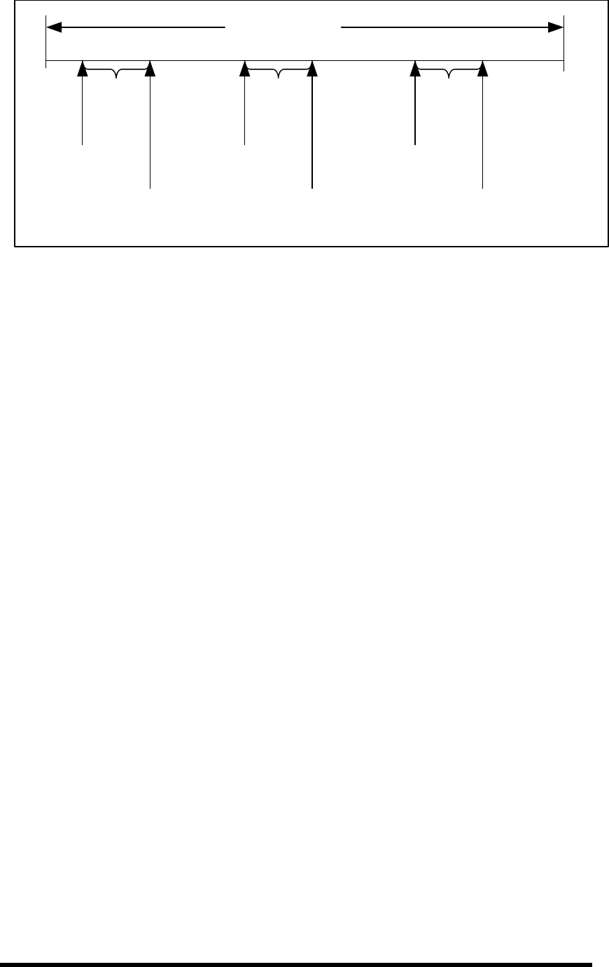
Toshiba Corporation Digital Media Network Company
Page 112 of 159
© 2004, Copyright TOSHIBA Corporation All Rights Reserved
LBA 0
User LBA space
LBA max
Test
span
1
Starting LBA for
test span 1
Ending LBA for
test span 1
Test
span
2
Starting LBA for
test span 2
Ending LBA for
test span 2
Test
span
3
Starting LBA for
test span 3
Ending LBA for
test span 3
Selective self-test test span example
After the scan of the selected spans described above, a user may wish to have the rest of media read scanned
as an off-line scan. In this case, the user shall set the flag to enable off-line scan in addition to the other settings.
If an error occurs during the scanning of the test spans, the error is reported in the self-test execution status in
the SMART READ DATA response and the off-line scan is not executed. When the test spans defined have
been scanned, the device shall then set the off-line scan pending and active flags in the Selective self-test log to
one, the span under test to a value greater than five, the self-test execution status in the SMART READ DATA
response to 00h, set a value of 03h in the off-line data collection status in the SMART READ DATA response
and shall proceed to do an off-line read scan through all areas not included in the test spans. This off-line read
scan shall completed as rapidly as possible, no pauses between block reads, and any errors encountered shall
not be reported to the host. Instead error locations may be logged for future reallocation. If the device is
powered-down before the off-line scan is completed, the off-line scan shall resume when the device is again
powered up. From power-up, the resumption of the scan shall be delayed the time indicated in the Selective
self-test pending time field in the Selective self-test log. During this delay time the pending flag shall be set to
one and the active flag shall be set to zero in the Selective self-test log. Once the time expires, the active flag
shall be set to one, and the off-line scan shall resume. When the entire media has been scanned, the off-line
scan shall terminate, both the pending and active flags shall be cleared to zero, and the off-line data collection
status in the SMART READ DATA response shall be set to 02h indicating completion.
During execution of the Selective self-test, the self-test executions time byte in the Device SMART Data
Structure may be updated but the accuracy may not be exact because of the nature of the test span segments.
For this reason, the time to complete off-line testing and the self-test polling times are not valid. Progress
through the test spans is indicated in the selective self-test log.
A hardware or software reset shall abort the Selective self-test except when the pending bit is set to one in the
Selective self-test log (see 11.8.42.6.5). The receipt of a SMART EXECUTE OFF-LINE IMMEDIATE command
with 0Fh, Abort off-line test routine, in the LBA Low register shall abort Selective self-test regardless of where
the device is in the execution of the command. If a second self-test is issued while a selective self-test is in
progress, the selective self-test is aborted and the newly requested self-test is executed.
Toshiba Corporation Digital Media Network Company
Page 113 of 159
© 2004, Copyright TOSHIBA Corporation All Rights Reserved
11.8.42.6 SMART Read Log Sector
COMMAND CODE 1 0 1 1 0 0 0 0 REGISTER
REGISTER SETTING NORMAL COMPLETION
DR DRIVE No. no change
CY C24Fh no change
HD no change
SN Log Sector Address no change
SC Number of sectors to read 00h
FT D5h no change
This command returns the indicated log sector contents to the host.
Sector count -specifies the number of sectors to be read from the specified log. The log transferred by the
drive shall start at the first sector in the specified log, regardless of the sector count requested.
Sector number indicates the log sector to be returned as described in the following Table.
Log Sector
Log sector address Content R/W
00h Log directory RO
01h SMART error log RO
02h Comprehensive SMART error log RO
03h Extended comprehensive SMART error log See Note
04h-05h Reserved RO
06h SMART self-test log RO
07h Extended SMART self-test log See Note
08h Reserved RO
09h Selective self-test log RO
0Ah-7Fh Reserved RO
80h-9Fh Host vendor specific R/W
A0h-FFh Reserved VS
Key −
RO –Log is read only by the host.
R/W –Log is read or written by the host.
VS –Log is vendor specific thus read/write ability is vendor specific.
NOTE - Log addresses 03hand 07h are used by the READ LOG EXT and WRITE LOG
EXT commands. If these log addresses are used with the SMART READ LOG
command, the device shall return command aborted.
11.8.42.6.1 SMART log directory
The following table defines the 512 bytes that make up the SMART Log Directory.The SMART Log Directory is
SMART Log address zero, and is defined as one sector long.
Toshiba Corporation Digital Media Network Company
Page 114 of 159
© 2004, Copyright TOSHIBA Corporation All Rights Reserved
SMART Log Directory
Byte Descriptions
0-1 SMART Logging Version
2 Number of sectors in the log at log address 1
3 Reserved
4 Number of sectors in the log at log address 2
5 Reserved
… …
510 Number of sectors in the log at log address 255
511 Reserved
The value of the SMART Logging Version word is set to 01h. Then the drive supports multi-sector SMART logs.
In addition, if the drive supports multi-sector logs, then the logs at log addresses 80-9Fh shall each be defined
as 16 sectors long.
11.8.42.6.2 Summary error log sector
The following Table defines the 512 bytes that make up the SMART summary error log sector.
SMART summary error log sector
Byte Descriptions
0 SMART error log version
1 Error log index
2-91 First error log data structure
92-181 Second error log data structure
182-271 Third error log data structure
272-361 Fourth error log data structure
362-451 Fifth error log data structure
452-453 Device error count
454-510 Reserved
511 Data structure checksum
11.8.42.6.2.1 Error log version
The value of the SMART error log version byte is set to 01h.
11.8.42.6.2.2 Error log data structure
An error log data structure will be presented for each of the last five errors reported by the device. These error
log data structure entries are viewed as a circular buffer. That is, the first error will create the first error log data
structure; the second error, the second error log structure; etc. The sixth error will create an error log data
structure that replaces the first error log data structure; the seventh error replaces the second error log structure,
etc. The error log pointer indicates the most recent error log structure. If fewer than five errors have occurred,
the unused error log structure entries will be zero filled. The following table describes the content of a valid error
log data structure.
Error log data structure
Byte Descriptions
n –n+11 First command data structure
N+12 –n+23 Second command data structure
N+24 –n+35 Third command data structure
N+36 – n+47 Fourth command data structure
N+48 – n+59 Fifth command data structure
N+60 – n+89 Error data structure

Toshiba Corporation Digital Media Network Company
Page 115 of 159
© 2004, Copyright TOSHIBA Corporation All Rights Reserved
11.8.42.6.2.3 Command data structure
The fifth command data structure will contain the command or reset for which the error is being reported. The
fourth command data structure should contain the command or reset that preceded the command or reset for
which the error is being reported, the third command data structure should contain the command or reset
preceding the one in the fourth command data structure, etc. If fewer than four commands and resets preceded
the command or reset for which the error is being reported, the unused command data structures will be zero
filled, for example, if only three commands and resets preceded the command or reset for which the error is
being reported, the first command data structure will be zero filled. In some devices, the hardware
implementation may preclude the device from reporting the commands that preceded the command for which
the error is being reported or that preceded a reset. In this case, the command data structures are zero filled.
If the command data structure represents a command or software reset, the content of the command data
structure will be as shown in the following Table.
Command data structure
Byte Descriptions
n Content of the Device Control register when the Command register was written.
n+1 Content of the Features register when the Command register was written.
n+2 Content of the Sector Count register when the Command register was written.
n+3 Content of the Sector Number register when the Command register was written.
n+4 Content of the Cylinder Low register when the Command register was written.
n+5 Content of the Cylinder High register when the Command register was written.
n+6 Content of the Device/Head register when the Command register was written.
n+7 Content written to the Command register.
n+8 Timestamp
n+9 Timestamp
n+10 Timestamp
n+11 Timestamp
Timestamp shall be the time since power-on in milliseconds when command acceptance occurred. This
timestamp may wrap around.
11.8.42.6.2.4 Error data structure
The error data structure will contain the error description of the command for which an error was reported
as described in the following table. Error data structure
Byte Descriptions
N Reserved
n+1 Content of the Error register after command completion occurred.
n+2 Content of the Sector Count register after command completion occurred.
n+3 Content of the Sector Number register after command completion occurred.
n+4 Content of the Cylinder Low register after command completion occurred.
n+5 Content of the Cylinder High register after command completion occurred.
n+6 Content of the Device/Head register after command completion occurred.
n+7 Content written to the Status register after command completion occurred.
n+8 - n+26 Extended error information
n+27 State
n+28 Life timestamp (least significant byte)
n+29 Life timestamp (most significant byte)
Extended error information will be vendor specific.
State will contain a value indicating the state of the device when command was written to the Command
register or the reset occurred as described in the following Table.

Toshiba Corporation Digital Media Network Company
Page 116 of 159
© 2004, Copyright TOSHIBA Corporation All Rights Reserved
State field values
Value State
x0h Unknown
x1h Sleep
x2h Standby
x3h Active/Idle with BSY cleared to zero
x4h Executing SMART off-line or self-test
x5h-xAh Reserved
xBh-xFh Vendor unique
The value of x is vendor specific and may be different for each state.
Sleep indicates the reset for which the error is being reported was received when the device was in the
Sleep mode.
Standby indicates the command or reset for which the error is being reported was received when the
device was in the Standby mode.
Active/Idle with BSY cleared to zero indicates the command or reset for which the error is being reported
was received when the device was in the Active or Idle mode and BSY was cleared to zero.
Executing SMART off-line or self-test indicates the command or reset for which the error is being reported
was received when the device was in the process of executing a SMART off-line or self-test.
Life timestamp will contain the power-on lifetime of the device in hours when command completion
occurred.
11.8.42.6.2.5 Device error count
The device error count field will contain the total number of errors attributable to the device that have been
reported by the device during the life of the device. These errors will include UNC errors, IDNF errors for
which the address requested was valid, servo errors, write fault errors, etc. This count will not include
errors attributed to the receipt of faulty commands such as commands codes not implemented by the
device or requests with invalid parameters or invalid addresses. If the maximum value for this field is
reached, the count will remain at the maximum value when additional errors are encountered and logged.
11.8.42.6.2.6 Data structure checksum
The data structure checksum is the two's complement of the sum of the first 511 bytes in the data structure.
Each byte will be added with unsigned arithmetic, and overflow will be ignored. The sum of all 512 bytes will be
zero when the checksum is correct. The checksum is placed in byte 511.
11.8.42.6.3 Comprehensive error log
The following defines the format of each of the sectors that comprise the SMART comprehensive error log. The
SMART Comprehensive error log provides logging for 28-bit addressing only. For 48-bit addressing see
11.8.43.2 . The size of the SMART comprehensive error log is 51 sectors. All multi-byte fields shown in this
structure follow the byte ordering described in 11.8.42.6.2.3 and 11.8.42.6.2.4. The comprehensive error log
data structures shall include UNC errors, IDNF errors for which the address requested was valid, servo errors,
write fault errors, etc. Comprehensive error log data structures shall not include errors attributed to the receipt of
faulty commands such as command codes not supported by the device or requests with invalid parameters or
invalid addresses.

Toshiba Corporation Digital Media Network Company
Page 117 of 159
© 2004, Copyright TOSHIBA Corporation All Rights Reserved
Comprehensive error log
Byte First sector Subsequent sectors
0 SMART error log version Reserved
1 Error log index Reserved
2-91 First error log data structure Data structure 5n+1
92-181 Second error log data structure Data structure 5n+2
182-271 Third error log data structure Data structure 5n+3
272-361 Fourth error log data structure Data structure 5n+4
362-451 Fifth error log data structure Data structure 5n+5
452-453 Device error count Reserved
454-510 Reserved Reserved
511 Data structure checksum Data structure checksum
n is the sector number within the log. The first sector is sector zero
11.8.42.6.3.1 Error log version
The value of the error log version byte shall be set to 01h.
11.8.42.6.3.2 Error log index
The error log index indicates the error log data structure representing the most recent error. If there have been
no error log entries, the error log index is set to zero. Valid values for the error log index are zero to 255.
11.8.42.6.3.3 Error log data structure
The error log is viewed as a circular buffer. The device may support from two to 51 error log sectors. When the
last supported error log sector has been filled, the next error shall create an error log data structure that replaces
the first error log data structure in sector zero. The next error after that shall create an error log data structure
that replaces the second error log data structure in sector zero. The sixth error after the log has filled shall
replace the first error log data structure in sector one, and so on.
The error log index indicates the most recent error log data structure. Unused error log data structures shall be
filled with zeros.
The content of the error log data structure entries is defined in 11.8.42.6.2.2.
11.8.42.6.3.4 Device error count
The device error count field is defined in 11.8.42.6.2.5.
11.8.42.6.3.5 Data structure checksum
The data structure checksum is defined in 11.8.42.6.2.6.
11.8.42.6.4 Self-test log sector
The following Table defines the 512 bytes that make up the SMART self-test log sector.

Toshiba Corporation Digital Media Network Company
Page 118 of 159
© 2004, Copyright TOSHIBA Corporation All Rights Reserved
Self-test log data structure
Byte Descriptions
0-1 Self-test log data structure revision number
2-25 First descriptor entry
26-49 Second descriptor entry
..... ............
482-505 Twenty-first descriptor entry
506-507 Vendor specific
508 Self-test index
509-510 Reserved
511 Data structure checksum
11.8.42.6.4.1 Self-test log data structure revision number
The value of the self-test log data structure revision number is set to 0001h.
11.8.42.6.4.2 Self-test log descriptor entry
This log is viewed as a circular buffer. The first entry will begin at byte 2, the second entry will begin at byte 26,
and so on until the twenty-second entry, that will replace the first entry. Then, the twenty-third entry will replace
the second entry, and so on. If fewer than 21 self-tests have been performed by the device, the unused
descriptor entries will be filled with zeroes.
The content of the self-test descriptor entry is shown in the following Table.
Self-test log descriptor entry
Byte Descriptions
n Content of the Sector Number
n+1 Content of the self-test execution status
n+2 Life timestamp (least significant byte).
n+3 Life timestamp (most significant byte).
n+4 Content of the self-test failure checkpoint
n+5 Failing LBA(least significant byte).
n+6 Failing LBA(next least significant byte).
n+7 Failing LBA(next most significant byte).
n+8 Failing LBA(most significant byte).
n+9 - n+23 Vendor specific.
Content of the Sector Number register will be the content of the Sector Number register when the nth self-test
subcommand was issued.
Content of the self-test execution status byte will be the content of the self-test execution status byte when the
nth self-test was completed
Life timestamp will contain the power-on lifetime of the device in hours when the nth self-test subcommand was
completed.
Content of the self-test failure checkpoint byte will be the content of the self-test failure checkpoint byte when the
nth self-test was completed.
The failing LBA will be the LBA of the uncorrectable sector that caused the test to fail. If the device
encountered more than one uncorrectable sector during the test, this field will indicate the LBA of the
first uncorrectable sector encountered. If the test passed or the test failed for some reason other than an
uncorrectable sector, the value of this field is undefined.

Toshiba Corporation Digital Media Network Company
Page 119 of 159
© 2004, Copyright TOSHIBA Corporation All Rights Reserved
11.8.42.6.4.3 Self-test index
The self-test index will point to the most recent entry. Initially, when the log is empty, the index will be set
to zero. It will be set to one when the first entry is made, two for the second entry, etc., until the 22nd
entry, when the index will be reset to one.
11.8.42.6.4.4 Data structure checksum
The data structure checksum is the two's complement of the sum of the first 511 bytes in the data
structure. Each byte will be added with unsigned arithmetic, and overflow will be ignored. The sum of all
512 bytes is zero when the checksum is correct. The checksum is placed in byte 511.
11.8.42.6.5 Selective self-test log
The Selective self-test log is a log that may be both written and read by the host. This log allows the host to
select the parameters for the self-test and to monitor the progress of the self-test. The following table defines the
content of the Selective self-test log.
Selective self-test log
Byte Description Read/write
0-1 Data structure revision number R/W
2-9 Starting LBA for test span 1 R/W
10-17 Ending LBA for test span 1 R/W
18-25 Starting LBA for test span 2 R/W
26-33 Ending LBA for test span 2 R/W
34-41 Starting LBA for test span 3 R/W
42-49 Ending LBA for test span 3 R/W
50-57 Starting LBA for test span 4 R/W
58-65 Ending LBA for test span 4 R/W
66-73 Starting LBA for test span 5 R/W
74-81 Ending LBA for test span 5 R/W
82-337 Reserved Reserved
338-491 Vendor specific Vendor specific
492-499 Current LBA under test Read
500-501 Current span under test Read
502-503 Feature flags R/W
504-507 Vendor specific Vendor specific
508-509 Selective self-test pending time R/W
510 Reserved Reserved
511 Data structure checksum R/W
11.8.42.6.5.1 Data structure revision number
The value of the data structure revision number filed shall be 01h. This value shall be written by the host and
returned unmodified by the device.
11.8.42.6.5.2 Test span definition
The Selective self-test log provides for the definition of up to five test spans. The starting LBA for each test span
is the LBA of the first sector tested in the test span and the ending LBA for each test span is the last LBA tested
in the test span. If the starting and ending LBA values for a test span are both zero, a test span is not defined
and not tested. These values shall be written by the host and returned unmodified by the device.
11.8.42.6.5.3 Current LBA under test

Toshiba Corporation Digital Media Network Company
Page 120 of 159
© 2004, Copyright TOSHIBA Corporation All Rights Reserved
The Current LBA under test field shall be written with a value of zero by the host. As the self-test progresses, the
device shall modify this value to contain the beginning LBA of the 65,536 sector block currently being tested.
When the self-test including the off-line scan between test spans has been completed, a zero value is placed in
this field.
11.8.42.6.5.4 Current span under test
The Current span under test field shall be written with a value of zero by the host. As the self-test progresses,
the device shall modify this value to contain the test span number of the current span being tested. If an off-line
scan between test spans is selected, a value greater then five is placed in this field during the off-line scan.
When the self-test including the off-line scan between test spans has been completed, a zero value is placed in
this field.
11.8.42.6.5.5 Feature flags
The Feature flags define the features of Selective self-test to be executed (see following table).
Selective self-test feature flags
Bit Description
0 Vendor specific
1 When set to one, perform off-line scan after selective test.
2 Vendor specific
3 When set to one, off-line scan after selective test is pending.
4 When set to one, off-line scan after selective test is active.
5-15 Reserved.
Bit (1) shall be written by the host and returned unmodified by the device. Bits (4:3) shall be written as zeros by
the host and the device shall modify them as the test progresses.
11.8.42.6.5.6 Selective self-test pending time
The selective self-test pending time is the time in minutes from power-on to the resumption of the off-line testing
if the pending bit is set. At the expiration of this time, sets the active bit to one, and resumes the off-line scan that
had begun before power-down.
11.8.42.6.5.7 Data structure checksum
The data structure checksum is the two's complement of the sum of the first 511 bytes in the data
structure. Each byte will be added with unsigned arithmetic, and overflow will be ignored. The sum of all
512 bytes is zero when the checksum is correct. The checksum is placed in byte 511.

Toshiba Corporation Digital Media Network Company
Page 121 of 159
© 2004, Copyright TOSHIBA Corporation All Rights Reserved
11.8.42.7 SMART Write Log Sector
COMMAND CODE 1 0 1 1 0 0 0 0 REGISTER
REGISTER SETTING NORMAL COMPLETION
DR DRIVE No. no change
CY C24Fh no change
HD no change
SN Log Sector Address no change
SC Number of sectors to write 00h
FT D6h no change
This command writes an indicated number of 512 byte data sectors to the indicated log.
Toshiba Corporation Digital Media Network Company
Page 122 of 159
© 2004, Copyright TOSHIBA Corporation All Rights Reserved
11.8.42.8 SMART Enable Operations
COMMAND CODE 1 0 1 1 0 0 0 0 REGISTER
REGISTER SETTING NORMAL COMPLETION
DR DRIVE No. no change
CY C24Fh no change
HD no change
SN no change
SC no change
FT D8h no change
This command enables access to all SMART capabilities of the drive. Prior to receipt of this command,
Parameters for drive failure prediction are neither monitored nor saved by the drive. The state of SMART
(either enabled or disabled) will be preserved by the drive across power cycles. Once enabled, the receipt
of subsequent SMART ENABLE OPERATIONS commands don’t affect any of the parameters for drive
failure prediction.
Upon receipt of this command from the host, the drive sets BSY, enables SMART capabilities and
functions, clears BSY and asserts INTRQ.
11.8.42.9 SMART Disable Operations
COMMAND CODE 1 0 1 1 0 0 0 0 REGISTER
REGISTER SETTING NORMAL COMPLETION
DR DRIVE No. no change
CY C24Fh no change
HD no change
SN no change
SC no change
FT D9h no change
This command disables all SMART capabilities within the drive including any and all timer functions related
exclusively to this function. After receipt of this command the drive may disable all SMART operations.
Parameters for drive failure prediction will no longer be monitored or saved by the drive. The state of
SMART (either enabled or disabled) will be preserved by the drive across power cycles.
Upon receipt of the SMART DISABLE OPERATIONS command from the host, the drive sets BSY, disables
SMART capabilities and functions, clears BSY and asserts INTRQ.
After receipt of this command by the drive, all other SMART commands, except for SMART ENABLE
OPERATIONS, are disabled and invalid and will be aborted by the drive (including SMART DISABLE
OPERATIONS commands) with an Aborted command error.
Toshiba Corporation Digital Media Network Company
Page 123 of 159
© 2004, Copyright TOSHIBA Corporation All Rights Reserved
11.8.42.10 SMART Return Status
COMMAND CODE 1 0 1 1 0 0 0 0 REGISTER
REGISTER SETTING NORMAL COMPLETION
DR DRIVE No. no change
CY C24Fh C24Fh/2CF4h
HD no change
SN no change
SC no change
FT DAh no change
If an impending failure is not predicted, the drive sets the Cylinder Low register to 4Fh and the Cylinder High
register to C2h. If an impending failure is predicted, the drive sets the Cylinder Low register to F4h and the
Cylinder High register to 2Ch.
This command is used to communicate the reliability status of the drive to the host’s request. Upon receipt of
this command the drive sets BSY, saves any parameters monitored by the drive to non-volatile memory and
checks the drive condition.
11.8.42.11 SMART Enable/Disable Automatic Off-line
COMMAND CODE 1 0 1 1 0 0 0 0 REGISTER
REGISTER SETTING NORMAL COMPLETION
DR DRIVE No. no change
CY C24Fh no change
HD no change
SN no change
SC 00h/F8h no change
FT DBh no change
This subcommand enables and disables the optional feature that causes the device to perform the set of off-line
data collection activities that automatically collect attribute data in an off-line mode and then save this data to the
device’s non-volatile memory. This subcommand may either cause the device automatically initiate or resume
performance of its off-line data collection activities; or this command may cause the automatic off-line data
collection feature to be disabled.
A value of zero written by the host into the device’s Sector Count register before issuing this subcommand will
cause the feature to be disabled. Disabling this feature does not preclude the device from saving attribute values
to non-volatile memory during some other normal operation such as during a power-on or power-off sequence or
during an error recovery sequence.
A value of F8h written by the host into the device’s Sector Count register before issuing this command will cause
this feature to be enabled. Any other non-zero value written by the host into this register before issuing this
subcommand is vendor specific.
Automatic off-line data collection is executed every 24 power-on hours.
Toshiba Corporation Digital Media Network Company
Page 124 of 159
© 2004, Copyright TOSHIBA Corporation All Rights Reserved
11.8.43 Read Log EXT (2Fh)
COMMAND CODE 0 0 1 0 1 1 1 1 REGISTER
REGISTER SETTING NORMAL COMPLETION
DR drive no. no change
LBA
Low Current
Previous log address
Reserved HOB=0
HOB=1 Reserved
Reserved
LBA
Mid Current
Previous Sector offset(7:0)
Sector offset(15:8) HOB=0
HOB=1 Reserved
Reserved
LBA
High Current
Previous Reserved
Reserved HOB=0
HOB=1 Reserved
Reserved
SC Current
Previous sector count(7:0)
sector count(15:8) HOB=0
HOB=1 Reserved
Reserved
FT Current
Previous Reserved
Reserved HOB=0
HOB=1 no change
no change
This command returns the specified log to the host. The device shall interrupt for each DRQ block
transferred.
Sector Count - Specifies the number of sectors to be read from the specified log. The log transferred by the
drive shall start at the sector in the specified log at the specified offset, regardless of the sector count
requested.
LBA Low - Specifies the log to be returned as described in the following Table.
LBA Mid - Specifies the first sector of the log to be read.
Log Sector
Log sector address Content R/W
00h Log directory RO
01h SMART error log See Note
02h Comprehensive SMART error log See Note
03h Extended comprehensive SMART error log RO
04h-05h Reserved -
06h SMART self-test log See Note
07h Extended SMART self-test log RO
08h Reserved -
09h Selective self-test log See Note
0Ah-7Fh Reserved -
80h-9Fh Host vendor specific R/W
A0h-FFh Reserved -
Key −
RO –Log is read only by the host.
R/W –Log is read or written by the host.
NOTE - Log addresses 01h,02,,06h and 09h are used by the SMART READ LOG
command commands. If these log addresses are used with the READ LOG EXT
command, the device shall return command aborted.
11.8.43.1 General Purpose Log Directory
The following table defines the 512 bytes that make up the General Purpose Log Directory.

Toshiba Corporation Digital Media Network Company
Page 125 of 159
© 2004, Copyright TOSHIBA Corporation All Rights Reserved
General Purpose Log Directory
Byte Descriptions
0-1 General Purpose Logging Version
2 Number of sectors in the log at log address 01h (7:0)
3 Number of sectors in the log at log address 01h (15:8)
4 Number of sectors in the log at log address 02h (7:0)
5 Number of sectors in the log at log address 02h (15:8)
…
256 10h sectors in the log at log address 80h
257 00h sectors in the log at log address 80h
…
510-511 Number of sectors in the log at log address FFh
The value of the General Purpose Logging Version word is 0001h.
The logs at log addresses 80-9Fh shall each be defined as 16 sectors long.
11.8.43.2 Extended Comprehensive SMART Error log
The fpllowing table defines the format of each of the sectors that comprise the Extended Comprehensive
SMART error log. The size of the Extended Comprehensive SMART error log is 64 sectors. Error log data
structures shall include UNC errors, IDNF errors for which the address requested was valid, servo errors, write
fault errors, etc. Error log data structures shall not include errors attributed to the receipt of faulty commands
such as command codes not implemented by the device or requests with invalid parameters or invalid
addresses.
All 28-bit entries contained in the Comprehensive SMART log, defined under section 11.8.42.6.3, shall also be
included in the Extended Comprehensive SMART error log with the 48-bit entries.
Extended Comprehensive SMART error log
Byte First sector Subsequent sectors
0 SMART error log version Reserved
1 Reserved Reserved
2 Error log index (7:0) Reserved
3 Error log index (15:8) Reserved
4-127 First error log data structure Data structure 4n+1
128-251 Second error log data structure Data structure 4n+2
252-375 Third error log data structure Data structure 4n+3
376-499 Fourth error log data structure Data structure 4n+4
500-501 Device error count Reserved
502-510 Reserved Reserved
511 Data structure checksum Data structure checksum
n is the sector number within the log. The first sector is sector zero
11.8.43.2.1 Error log version
The value of the SMART error log version byte is 01h.
11.8.43.2.2 Error log index
The error log index indicates the error log data structure representing the most recent error. If there have been
no error log entries, the error log index is cleared to zero. Valid values for the error log index are zero to 255.

Toshiba Corporation Digital Media Network Company
Page 126 of 159
© 2004, Copyright TOSHIBA Corporation All Rights Reserved
11.8.43.2.3 Extended Error log data structure
The error log is viewed as a circular buffer. When the last supported error log sector has been filled, the next
error shall create an error log data structure that replaces the first error log data structure in sector zero. The
next error after that shall create an error log data structure that replaces the second error log data structure in
sector zero. The fifth error after the log has filled shall replace the first error log data structure in sector one, and
so on.
The error log index indicates the most recent error log data structure. Unused error log data structures shall be
filled with zeros.
The content of the error log data structure entries is defined in the following table.
Extended Error log data structure
Byte Descriptions
n thru n+17 First command data structure
n+18 thru n+35 Second command data structure
n+36 thru n+53 Third command data structure
n+54 thru n+71 Fourth command data structure
n+72 thru n+89 Fifth command data structure
n+90 thru n+123 Error data structure
11.8.43.2.3.1 Command data structure
The fifth command data structure shall contain the command or reset for which the error is being reported. The
fourth command data structure should contain the command or reset that preceded the command or reset for
which the error is being reported, the third command data structure should contain the command or reset
preceding the one in the fourth command data structure, etc. If fewer than four commands and resets preceded
the command or reset for which the error is being reported, the unused command data structures shall be zero
filled, for example, if only three commands and resets preceded the command or reset for which the error is
being reported, the first command data structure shall be zero filled. In some devices, the hardware
implementation may preclude the device from reporting the commands that preceded the command for which
the error is being reported or that preceded a reset. In this case, the command data structures are zero filled.
If the command data structure represents a command or software reset, the content of the command data
structure shall be as shown in the following table. If the command data structure represents a hardware reset,
the content of byte n shall be FFh, the content of bytes n+1 through n+13 are vendor specific, and the content of
bytes n+14 through n+17 shall contain the timestamp.

Toshiba Corporation Digital Media Network Company
Page 127 of 159
© 2004, Copyright TOSHIBA Corporation All Rights Reserved
Command data structure
Byte Descriptions
n Content of the Device Control register when the Command register was written.
N+1 Content of the Features register (7:0) when the Command register was written. (see note)
n+2 Content of the Features register (15:8) when the Command register was written.
N+3 Content of the Sector Count register (7:0) when the Command register was written.
N+4 Content of the Sector Count register (15:8) when the Command register was written.
N+5 Content of the LBA Low register (7:0) when the Command register was written.
N+6 Content of the LBA Lowregister (15:8) when the Command register was written.
N+7 Content of the LBA Mid register (7:0) when the Command register was written.
N+8 Content of the LBA Mid register (15:8) when the Command register was written.
N+9 Content of the LBA High register (7:0) when the Command register was written.
N+10 Content of the LBA High register (15:8) when the Command register was written.
N+11 Content of the Device/Head register when the Command register was written.
N+12 Content written to the Command register.
N+13 Reserved
n+14 Timestamp (least significant byte)
n+15 Timestamp (next least significant byte)
n+16 Timestamp (next most significant byte)
n+17 Timestamp (most significant byte)
NOTE - bits (7:0) refer to the most recently written contents of the register. Bits (15:8) refer to the
contents of the register prior to the most recent write to the register.
Timestamp shall be the time since power-on in milliseconds when command acceptance occurred. This
timestamp may wrap around.
11.8.43.2.3.2 Error data structure
The error data structure shall contain the error description of the command for which an error was reported as
described in the following table. If the error was logged for a hardware reset, the content of bytes n+1 through
n+11 shall be vendor specific and the remaining bytes shall be as defined in the following table.
Toshiba Corporation Digital Media Network Company
Page 128 of 159
© 2004, Copyright TOSHIBA Corporation All Rights Reserved
Error data structure
Byte Descriptions
n Reserved
n+1 Content of the Error register after command completion occurred.
N+2 Content of the Sector Count register (7:0) after command completion occurred. (see note)
n+3 Content of the Sector Count register (15:8) after command completion occurred. (see note)
n+4 Content of the LBA Low register (7:0) after command completion occurred.
N+5 Content of the LBA Low register (15:8) after command completion occurred.
N+6 Content of the LBA Mid register (7:0) after command completion occurred.
N+7 Content of the LBA Mid register (15:8) after command completion occurred.
N+8 Content of the LBA High register (7:0) after command completion occurred.
N+9 Content of the LBA High register (15:8) after command completion occurred.
N+10 Content of the Device/Head register after command completion occurred.
N+11 Content written to the Status register after command completion occurred.
N+12
through
n+30
Extended error information
n+31 State
n+32 Life timestamp (least significant byte)
n+33 Life timestamp (most significant byte)
NOTE - bits (7:0) refer to the contents if the register were read with bit 7 of the Device Control register
cleared to zero. Bits (15:8) refer to the contents if the register were read with bit 7 of the Device
Control register set to one.
State shall contain a value indicating the state of the device when the command was written to the Command
register or the reset occurred as described in the following table.
State field values
Value State
x0h Unknown
x1h Sleep
x2h Standby
x3h Active/Idle with BSY cleared to zero
x4h Executing SMART off-line or self-test
x5h-xFh Reserved
The value of x is vendor specific and may be different for each state.
Sleep indicates the reset for which the error is being reported was received when the device was in the Sleep
mode.
Standby indicates the command or reset for which the error is being reported was received when the device was
in the Standby mode.
Active/Idle with BSY cleared to zero indicates the command or reset for which the error is being reported was
received when the device was in the Active or Idle mode and BSY was cleared to zero.
Executing SMART off-line or self-test indicates the command or reset for which the error is being reported was
received when the device was in the process of executing a SMART off-line or self-test.
Life timestamp shall contain the power-on lifetime of the device in hours when command completion occurred.
11.8.43.2.4 Device error count
The device error count field shall contain the total number of errors attributable to the device that have been
reported by the device during the life of the device. These errors shall include UNC errors, IDNF errors for which
the address requested was valid, servo errors, write fault errors, etc. This count shall not include errors
Toshiba Corporation Digital Media Network Company
Page 129 of 159
© 2004, Copyright TOSHIBA Corporation All Rights Reserved
attributed to the receipt of faulty commands such as commands codes not implemented by the device or
requests with invalid parameters or invalid addresses. If the maximum value for this field is reached, the count
shall remain at the maximum value when additional errors are encountered and logged.
11.8.43.2.5 Data structure checksum
The data structure checksum is the two’s complement of the sum of the first 511 bytes in the data structure.
Each byte shall be added with unsigned arithmetic, and overflow shall be ignored. The sum of all 512 bytes will
be zero when the checksum is correct. The checksum is placed in byte 511.
11.8.43.3 Extended Self-test log sector
The following table defines the format of each of the sectors that comprise the Extended SMART Self-test log.
The size of the self-test log is 1 sectors.
The Extended SMART self-test log sector shall support 48-bit and 28-bit addressing. All 28-bit entries
contained in the SMART self-test log, defined under section 11.8.42.6.4 shall also be included in the Extended
SMART self-test log with all 48-bit entries.
Extended Self-test log data structure
Byte First sector Subsequent sectors
0 Self-test log data structure revision number Reserved
1 Reserved Reserved
2 Self-test descriptor index (7:0) Reserved
3 Self-test descriptor index (15:8) Reserved
4-29 Descriptor entry 1 Descriptor entry 18n+1
30-55 Descriptor entry 2 Descriptor entry 18n+2
…. .... ....
472-497 Descriptor entry 18 Descriptor entry 18n+18
498-499 Vendor specific Vendor specific
500-510 Reserved Reserved
511 Data structure checksum Data structure checksum
n is the sector number within the log. The first sector is sector zero
This log is viewed as a circular buffer. The first entry will begin at byte 4, the second entry will begin at byte 30
and so on until the nineteen entry, that will replace the first entry. Then, the twenty entry will replace the
second entry, and so on. If fewer than 18 self-tests have been performed by the device, the unused descriptor
entries will be filled with zeroes.
11.8.43.3.1 Self-test descriptor index
The Self-test descriptor index indicates the most recent self-test descriptor. If there have been no self-tests, the
Self-test descriptor index is set to zero. Valid values for the Self-test descriptor index are zero to 18.
11.8.43.3.2 Self-test log data structure revision number
The value of the self-test log data structure revision number is 01h.
11.8.43.3.3 Extended Self-test log descriptor entry
The content of the self-test descriptor entry is shown in the following table..

Toshiba Corporation Digital Media Network Company
Page 130 of 159
© 2004, Copyright TOSHIBA Corporation All Rights Reserved
Extended Self-test log descriptor entry
Byte Descriptions
n Content of the LBA Low register.
n+1 Content of the self-test execution status byte.
n+2 Life timestamp (least significant byte).
n+3 Life timestamp (most significant byte).
n+4 Content of the self-test failure checkpoint byte.
n+5 Failing LBA (7:0).
n+6 Failing LBA (15:8).
n+7 Failing LBA (23:16).
n+8 Failing LBA (31:24).
n+9 Failing LBA (39:32).
n+10 Failing LBA (47:40).
n+1 - n+23 Vendor specific.
Content of the LBA Low register shall be the content of the LBA Low register when the nth self-test
subcommand was issued (see 11.8.42.5 ).
Content of the self-test execution status byte shall be the content of the self-test execution status byte when the
nth self-test was completed (see 11.8.42.5).
Life timestamp shall contain the power-on lifetime of the device in hours when the nth self-test subcommand
was completed.
Content of the self-test failure checkpoint byte may contain additional information about the self-test that failed.
The failing LBA shall be the LBA of the sector that caused the test to fail. If the device encountered more than
one failed sector during the test, this field shall indicate the LBA of the first failed sector encountered. If the test
passed or the test failed for some reason other than a failed sector, the value of this field is undefined.
11.8.43.3.4 Data structure checksum
The data structure checksum is the two's complement of the sum of the first 511 bytes in the data structure.
Each byte shall be added with unsigned arithmetic, and overflow shall be ignored. The sum of all 512 bytes is
zero when the checksum is correct. The checksum is placed in byte 511.

Toshiba Corporation Digital Media Network Company
Page 131 of 159
© 2004, Copyright TOSHIBA Corporation All Rights Reserved
11.8.44 Write Log EXT (3Fh)
COMMAND CODE 0 0 1 1 1 1 1 1 REGISTER
REGISTER SETTING NORMAL COMPLETION
DR drive no. no change
LBA
Low Current
Previous log address
Reserved HOB=0
HOB=1 Reserved
Reserved
LBA
Mid Current
Previous Sector offset(7:0)
Sector offset(15:8) HOB=0
HOB=1 Reserved
Reserved
LBA
High Current
Previous Reserved
Reserved HOB=0
HOB=1 Reserved
Reserved
SC Current
Previous sector count(7:0)
sector count(15:8) HOB=0
HOB=1 Reserved
Reserved
FT Current
Previous Reserved
Reserved HOB=0
HOB=1 no change
no change
This command writes a specified number of 512 byte data sectors to the specified log. The device shall
interrupt for each DRQ block transferred.

Toshiba Corporation Digital Media Network Company
Page 132 of 159
© 2004, Copyright TOSHIBA Corporation All Rights Reserved
11.8.45 Device Configuration (B1h)
This command has a number of separate functions which can be selected via the Feature Register when the
command is issued. The subcommands and their respective codes are listed below.
Subcommand Feature Register
DEVICE CONFIGURATION RESTORE C0h
DEVICE CONFIGURATION FREEZE LOCK C1h
DEVICE CONFIGURATION IDENTIFY C2h
DEVICE CONFIGURATION SET C3h
11.8.45.1 Device Configuration Restore
COMMAND CODE 1 0 1 1 0 0 0 1 REGISTER
REGISTER SETTING NORMAL COMPLETION
DR DRIVE No. no change
CY na no change
HD na no change
SN na no change
SC na no change
FT C0h no change
LBA na no change
The DEVICE CONFIGURATION RESTORE command disables any setting previously made by a DEVICE
CONFIGURATION SET command and returns the content of the IDENTIFY DEVICE or IDENTIFY PACKET
DEVICE command response to the original settings as indicated by the data returned from the execution of a
DEVICE CONFIGURATION IDENTIFY command.
11.8.45.2 Device Configuration Freeze Lock
COMMAND CODE 1 0 1 1 0 0 0 1 REGISTER
REGISTER SETTING NORMAL COMPLETION
DR DRIVE No. no change
CY na no change
HD na no change
SN na no change
SC na no change
FT C1h no change
LBA na no change

Toshiba Corporation Digital Media Network Company
Page 133 of 159
© 2004, Copyright TOSHIBA Corporation All Rights Reserved
The DEVICE CONFIGURATION FREEZE LOCK command prevents accidental modification of the Device
Configuration Overlay settings. After successful execution of a DEVICE CONFIGURATION FREEZE LOCK
command, all DEVICE CONFIGURATION SET, DEVICE CONFIGURATION FREEZE LOCK, DEVICE
CONFIGURATION IDENTIFY, and DEVICE CONFIGURATION RESTORE commands are aborted by the
device. The DEVICE CONFIGURATION FREEZE LOCK condition shall be cleared by a power-down. The
DEVICE CONFIGURATION FREEZE LOCK condition shall not be cleared by hardware or software reset.
11.8.45.3 Device Configuration Identify
COMMAND CODE 1 0 1 1 0 0 0 1 REGISTER
REGISTER SETTING NORMAL COMPLETION
DR DRIVE No. no change
CY na no change
HD na no change
SN na no change
SC na no change
FT C2h no change
LBA na no change
The DEVICE CONFIGURATION IDENTIFY command returns a 512 byte data structure via PIO data-in transfer.
The content of this data structure indicates the selectable commands, modes, and feature sets that the device is
capable of supporting. If a DEVICE CONFIGURATION SET command has been issued reducing the
capabilities, the response to an IDENTIFY DEVICE or IDENTIFY PACKET DEVICE command will reflect the
reduced set of capabilities, while the DEVICE CONFIGURATION IDENTIFY command will reflect the entire set
of selectable capabilities.
The format of the Device Configuration Overlay data structure is shown in Table 11.8-8.
Table 11.8-8 Device Configuration Identify data stracture

Toshiba Corporation Digital Media Network Company
Page 134 of 159
© 2004, Copyright TOSHIBA Corporation All Rights Reserved
Word Content
0 Data structure revision
1 Multiword DMA modes supported
15-3 Reserved
2 1 = Multiword DMA mode 2 and below are supported
1 1 = Multiword DMA mode 1 and below are supported
0 1 = Multiword DMA mode 0 is supported
2 Ultra DMA modes supported
15-5 Reserved
5 1 = Ultra DMA mode 5 and below are supported
4 1 = Ultra DMA mode 4 and below are supported
3 1 = Ultra DMA mode 3 and below are supported
2 1 = Ultra DMA mode 2 and below are supported
1 1 = Ultra DMA mode 1 and below are supported
0 1 = Ultra DMA mode 0 is supported
3-6 Maximum LBA address
7 Command set/feature set supported
15-9 Reserved
8 1 = 48-bit Addressing feature set supported
7 1 = Host Protected Area feature set supported
6 1 = Automatic acoustic management supported
5 1 = READ/WRITE DMA QUEUED commands supported
4 1 = Power-up in Standby feature set supported
3 1 = Security feature set supported
2 1 = SMART error log supported
1 1 = SMART self-test supported
0 1 = SMART feature set supported
8-254 Reserved
255 Integrity word
15-8 Checksum
7-0 Signature
11.8.45.3.1.1 Word 0: Data structure revision
Word 0 shall contain the value 0001h.
11.8.45.3.1.2 Word 1: Multiword DMA modes supported
Word 2 bits 2-0 contain the same information as contained in word 63 of the IDENTIFY DEVICE or IDENTIFY
PACKET DEVICE command response. Bits 15-3 of word 2 are reserved.
11.8.45.3.1.3 Word 2: Ultra DMA modes supported
Word 3 bits 5-0 contain the same information as contained in word 88 of the IDENTIFY DEVICE or IDENTIFY
PACKET DEVICE command response. Bits 15-6 of word 3 are reserved.
11.8.45.3.1.4 Words 3-6: Maximum LBA address
Words 4 through 7 define the maximum LBA address. This is the highest address accepted by the device in the
factory default condition. If no DEVICE CONFIGURATION SET command has been executed modifying the
factory default condition, this is the same value as that returned by a READ NATIVE MAX ADDRESS or READ
NATIVE MAX ADDRESS EXT command.

Toshiba Corporation Digital Media Network Company
Page 135 of 159
© 2004, Copyright TOSHIBA Corporation All Rights Reserved
11.8.45.3.1.5 Word 7: Command/features set supported
Word 7 bit 0 if set to one indicates that the device is capable of supporting the SMART feature set.
Word 7 bit 1 if set to one indicates that the device is capable of supporting SMART self-test including the
self-test log.
Word 7 bit 2 if set to one indicates that the device is capable of supporting SMART error logging.
Word 7 bit 3 if set to one indicates that the device is capable of supporting the Security feature set.
Word 7 bit 4 if set to one indicates that the device is capable of supporting the Power-up in Standby feature set.
Word 7 bit 5 if set to one indicates that the device is capable of supporting the READ DMA QUEUED and
WRITE DMA QUEUED commands.
Word 7 bit 6 if set to one indicates that the device is capable of supporting the Automatic Acoustic Management
feature set.
Word 7 bit 7 if set to one indicates that the device is capable of supporting the Host Protected Area feature set.
Word 7 bit 8 if set to one indicates that the device is capable of supporting the 48-bit Addressing feature set.
Word 7 bits 9 through 15 are reserved.
11.8.45.3.1.6 Words 8-254: Reserved
11.8.45.3.1.7 Word 255: Integrity word
Bits 7:0 of this word shall contain the value A5h. Bits 15:8 of this word shall contain the data structure checksum.
The data structure checksum shall be the two’s complement of the sum of all byte in words 0 through 254 and
the byte consisting of bits 7:0 of word 255. Each byte shall be added with unsigned arithmetic, and overflow shall
be ignored. The sum of all bytes is zero when the checksum is correct.
11.8.45.4 Device Configuration Set
COMMAND CODE 1 0 1 1 0 0 0 1 REGISTER
REGISTER SETTING NORMAL COMPLETION
DR DRIVE No. no change
CY na no change
HD na no change
SN na no change
SC na no change
FT C3h no change
LBA na no change

Toshiba Corporation Digital Media Network Company
Page 136 of 159
© 2004, Copyright TOSHIBA Corporation All Rights Reserved
11.8.45.4.1 Error outputs
Register 7 6 5 4 3 2 1 0
Error na na na na na ABRT na na
Sector Count na
Sector Number Bit location low
Cylinder Low Bit location high
Cylinder High Word location
Device/Head obs na obs DEV na
Status BSY DRD
Y DF na DRQ na na ERR
Error register -
ABRT shall be set to one if the device does not support this command, if a DEVICE CONFIGURATION
SET command has already modified the original settings as reported by a DEVICE
CONFIGURATION IDENTIFY command, if DEVICE CONFIGURATION FREEZE LOCK is set, if
any of the bit modification restrictions described in this section are violated, or if a Host
Protected Area has been established by the execution of a SET MAX ADDRESS command.
Sector Number –
If the command was aborted because an attempt was made to modify a mode or feature that cannot be
modified with the device in its current state, this register shall contain bits (7:0) set in the bit
positions that correspond to the bits in the device configuration overlay data structure words 1,
2, or 7 for each mode or feature that cannot be changed. If not, the value shall be 00h.
Cylinder Low –
If the command was aborted because an attempt was made to modify a mode or feature that cannot be
modified with the device in its current state, this register shall contain bits (15:8) set in the bit
positions that correspond to the bits in the device configuration overlay data structure words 1,
2, or 7 for each mode or feature that cannot be changed. If not, the value shall be 00h.
Cylinder High –
If the command was aborted because an attempt was made to modify a bit that cannot be modified with
the device in its current state, this register shall contain the offset of the first word encountered
that cannot be changed. If an illegal maximum LBA address is encountered, the offset of word 3
shall be entered. If a checksum error occurred, the value FFh shall be entered. A value of 00h
indicates that the Data Structure Revision was invalid.
Device register -
DEV shall indicate the selected device.
Status register -
BSY shall be cleared to zero indicating command completion.
DRDY shall be set to one.
DF (Device Fault) shall be set to one if a device fault has occurred.
DRQ shall be cleared to zero.
ERR shall be set to one if an Error register bit is set to one.
11.8.45.4.2 Description
The DEVICE CONFIGURATION SET command allows a device manufacturer or a personal computer system
manufacturer to reduce the set of optional commands, modes, or feature sets supported by a device as
indicated by a DEVICE CONFIGURATION IDENTIFY command. The DEVICE CONFIGURATION SET
command transfers an overlay that modifies some of the bits set in words 63, 82, 83, 84, and 88 of the
IDENTIFY DEVICE or IDENTIFY PACKET DEVICE command response. When the bits in these words are
cleared, the device shall no longer support the indicated command, mode, or feature set. If a bit is set in the
overlay transmitted by the device that is not set in the overlay received from a DEVICE CONFIGURATION
IDENTIFY command, no action is taken for that bit. Modifying the maximum LBA address of the device also
modifies the address value returned by a READ NATIVE MAX ADDRESS or READ NATIVE MAX ADDRESS
EXT command.

Toshiba Corporation Digital Media Network Company
Page 137 of 159
© 2004, Copyright TOSHIBA Corporation All Rights Reserved
The format of the overlay transmitted by the device is described inTable 11.8-9. The restrictions on changing
these bits is described in the text following Table 11.8-9. If any of the bit modification restrictions described are
violated, the device shall return command aborted.
Table 11.8-9 Device Configuration Overlay data stracture
Word Content
0 Data structure revision
1 Multiword DMA modes supported
15-3 Reserved
2 1 = Multiword DMA mode 2 and below are supported
1 1 = Multiword DMA mode 1 and below are supported
0 1 = Multiword DMA mode 0 is supported
2 Ultra DMA modes supported
15-5 Reserved
5 1 = Ultra DMA mode 5 and below are supported
4 1 = Ultra DMA mode 4 and below are supported
3 1 = Ultra DMA mode 3 and below are supported
2 1 = Ultra DMA mode 2 and below are supported
1 1 = Ultra DMA mode 1 and below are supported
0 1 = Ultra DMA mode 0 is supported
3-6 Maximum LBA address
7 Command set/feature set supported
15-9 Reserved
8 1 = 48-bit Addressing feature set supported
7 1 = Host Protected Area feature set supported
6 1 = Automatic acoustic management supported
5 1 = READ/WRITE DMA QUEUED commands supported
4 1 = Power-up in Standby feature set supported
3 1 = Security feature set supported
2 1 = SMART error log supported
1 1 = SMART self-test supported
0 1 = SMART feature set supported
8-254 Reserved
255 Integrity word
15-8 Checksum
7-0 Signature
11.8.45.4.2.1 Word 0: Data structure revision
Word 0 shall contain the value 0001h.
11.8.45.4.2.2 Word 1: Multiword DMA modes supported
Word 1 bits 15:3 are reserved.
Word 1 bit 2 is cleared to disable support for Multiword DMA mode 2 and has the effect of clearing bit 2 in word
63 of the IDENTIFY DEVICE or IDENTIFY PACKET DEVICE response. This bit shall not be cleared if Multiword
DMA mode 2 is currently selected.
Word 1 bit 1 is cleared to disable support for Multiword DMA mode 1 and has the effect of clearing bit 1 in word
63 of the IDENTIFY DEVICE or IDENTIFY PACKET DEVICE response. This bit shall not be cleared if Multiword
DMA mode 2 is supported or Multiword DMA mode 1 or 2 is selected.
Word 1 bit 0 shall not be cleared.

Toshiba Corporation Digital Media Network Company
Page 138 of 159
© 2004, Copyright TOSHIBA Corporation All Rights Reserved
11.8.45.4.2.3 Word 2: Ultra DMA modes supported
Word 2 bits 15:6 are reserved.
Word 2 bit 5 is cleared to disable support for Ultra DMA mode 5 and has the effect of clearing bit 5 in word 88 of
the IDENTIFY DEVICE or IDENTIFY PACKET DEVICE response. This bit shall not be cleared if Ultra DMA
mode 5 is currently selected.
Word 2 bit 4 is cleared to disable support for Ultra DMA mode 4 and has the effect of clearing bit 4 in word 88 of
the IDENTIFY DEVICE or IDENTIFY PACKET DEVICE response. This bit shall not be cleared if Ultra DMA
mode 5 is supported or if Ultra DMA mode 5 or 4 is selected.
Word 2 bit 3 is cleared to disable support for Ultra DMA mode 3 and has the effect of clearing bit 3 in word 88 of
the IDENTIFY DEVICE or IDENTIFY PACKET DEVICE response. This bit shall not be cleared if Ultra DMA
mode 5 or 4 is supported or if Ultra DMA mode 5, 4, or 3 is selected.
Word 2 bit 2 is cleared to disable support for Ultra DMA mode 2 and has the effect of clearing bit 2 in word 88 of
the IDENTIFY DEVICE or IDENTIFY PACKET DEVICE response. This bit shall not be cleared if Ultra DMA
mode 5, 4, or 3 is supported or if Ultra DMA mode 5, 4, 3, or 2 is selected.
Word 2 bit 1 is cleared to disable support for Ultra DMA mode 1 and has the effect of clearing bit 1 in word 88 of
the IDENTIFY DEVICE or IDENTIFY PACKET DEVICE response. This bit shall not be cleared if Ultra DMA
mode 5, 4, 3, or 2 is supported or if Ultra DMA mode 5, 4, 3, 2, or 1 is selected.
Word 2 bit 0 is cleared to disable support for Ultra DMA mode 0 and has the effect of clearing bit 0 in word 88 of
the IDENTIFY DEVICE or IDENTIFY PACKET DEVICE response. This bit shall not be cleared if Ultra DMA
mode 5, 4, 3, 2, or 1 is supported or if Ultra DMA mode 5, 4, 3, 2, 1, or 0 is selected.
11.8.45.4.2.4 Words 3-6: Maximum LBA address
Words 3 through 6 define the maximum LBA address. This shall be the highest address accepted by the device
after execution of the command. When this value is changed, the content of IDENTIFY DEVICE words 60, 61
100, 101, 102, and103 shall be changed as described in the SET MAX ADDRESS and SET MAX ADDRESS
EXT command descriptions to reflect the maximum address set with this command. This value shall not be
changed and command aborted shall be returned if a Host Protected Area has been established by the
execution of a SET MAX ADDRESS or SET MAX ADDRESS EXT command with an address value less than
that returned by a READ NATIVE MAX ADDRESS or READ NATIVE MAX ADDRESS EXT command.. Any data
contained in the Host Protected Area is not affected.
11.8.45.4.2.5 Word 7: Command/features set supported
Word 7 bits 15:9 are reserved.
Word 7 bit 8 is cleared to disable support for the 48-bit Addressing feature set and has the effect of clearing bit
10 in words 83 and 86 and clearing the value in words 103:100 of the IDENTIFY DEVICE or IDENTIFY PACKET
DEVICE response.
Word 7 bit 7 is cleared to disable support for the Host Protected Area feature set and has the effect of clearing
bit 10 in words 82 and 85 and clearing bit 8 in words 83 and 86 of the IDENTIFY DEVICE or IDENTIFY PACKET
DEVICE response. If a Host Protected Area has been established by use of the SET MAX ADDRESS command,
these bits shall not be cleared and the device shall return command aborted.
Word 7 bit 6 is cleared to disable for the Automatic Acoustic Management feature set and has the effect of
clearing bit 9 in word 83 and word 94 of the IDENTIFY DEVICE or IDENTIFY PACKET DEVICE response.

Toshiba Corporation Digital Media Network Company
Page 139 of 159
© 2004, Copyright TOSHIBA Corporation All Rights Reserved
Word 7 bit 5 is cleared to disable support for the READ DMA QUEUED and WRITE DMA QUEUED commands
and has the effect of clearing bit 1 in words 83 and 86 of the IDENTIFY DEVICE or IDENTIFY PACKET DEVICE
response.
Word 7 bit 4 is cleared to disable support for the Power-up in Standby feature set and has the effect of clearing
bits 5 and 6 in words 83 and 86 and clearing the value in word 94 of the IDENTIFY DEVICE or IDENTIFY
PACKET DEVICE response. If Power-up in Standby has been enabled by a jumper, these bits shall not be
cleared.
Word 7 bit 3 is cleared to disable support for the Security feature set and has the effect of clearing bit 1 in words
82 and 85 of the IDENTIFY DEVICE or IDENTIFY PACKET DEVICE response. These bits shall not be cleared if
the Security feature set has been enabled.
Word 7 bit 2 is cleared to disable support for the SMART error logging and has the effect of clearing bit 0 in
words 84 and 87 of the IDENTIFY DEVICE or IDENTIFY PACKET DEVICE response.
Word 7 bit 1 is cleared to disable support for the SMART self-test and has the effect of clearing bit 1 in words 84
and 87 of the IDENTIFY DEVICE or IDENTIFY PACKET DEVICE response.
Word 7 bit 0 is cleared to disable support for the SMART feature set and has the effect of clearing bit 0 in words
82 and 85 of the IDENTIFY DEVICE or IDENTIFY PACKET DEVICE response. If bits 1 and 2 of word 7 are not
cleared to zero or if the SMART feature set has been enabled by use of the SMART ENABLE OPERATIONS
command, these bits shall not be cleared and the device shall return command aborted.
11.8.45.4.2.6 Words 8-254: Reserved
11.8.45.4.2.7 Word 255: Integrity word
Bits 7:0 of this word shall contain the value A5h. Bits 15:8 of this word shall contain the data structure checksum.
The data structure checksum shall be the two’s complement of the sum of all byte in words 0 through 254 and
the byte consisting of bits 7:0 of word 255. Each byte shall be added with unsigned arithmetic, and overflow shall
be ignored. The sum of all bytes is zero when the checksum is correct.

Toshiba Corporation Digital Media Network Company
Page 140 of 159
© 2004, Copyright TOSHIBA Corporation All Rights Reserved
11.9 Security Mode Feature Set
The Security mode features allow the host to implement a security password system to prevent
unauthorized access to the disk drive.
• Following Commands are supported for this feature set .
• SECURITY SET PASSWORD
• SECURITY UNLOCK
• SECURITY ERASE PREPARE
• SECURITY ERASE UNIT
• SECURITY FREEZE LOCK
• SECURITY DISABLE PASSWORD
Parameter word for the Security mode feature set is described in IDENTIFY DEVICE response Word 128.
11.9.1 Security mode default setting
The drive is shipped with the master password set to 20h value (ASCII blanks) and the lock function disabled.
The system manufacturer/dealer may set a new master password by using the SECURITY SET PASSWORD
command, without enabling the lock function.
If the Master Password Revision Code feature is supported, the Master Password Revision Code is initially
set to FFFEh.
11.9.2 Initial setting of the user password
When a user password is set, the drive automatically enters lock mode by the next powered-on .
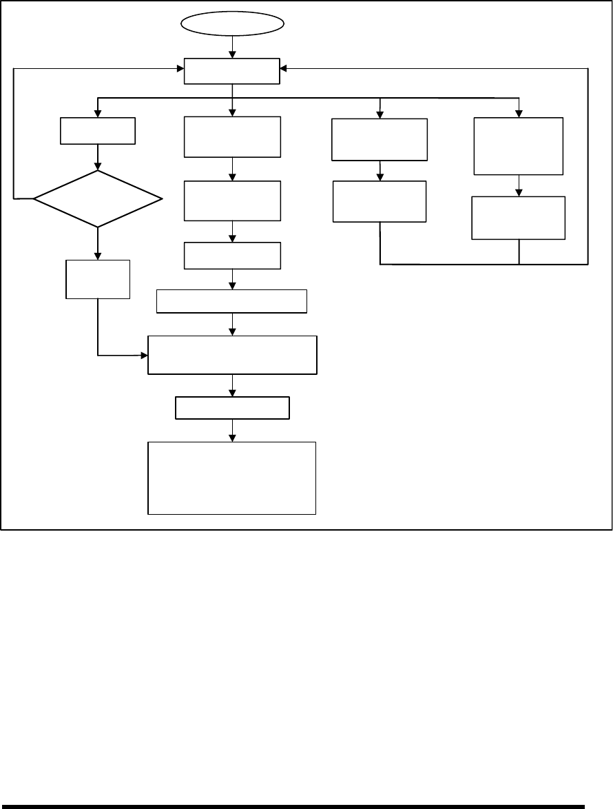
Toshiba Corporation Digital Media Network Company
Page 141 of 159
© 2004, Copyright TOSHIBA Corporation All Rights Reserved
11.9.3 Security mode operation from power-on
In locked mode, the drive rejects media access commands until a SECURITY UNLOCK command is
successfully completed.
Power-on
Locked mode
UNLOCK ERASE Media access Non-media
PREPARE access
No
Password ERASE Reject
match? UNIT Command Execute
Command
Yes
Unit erased
Unlock
mode
Lock function disabled
Normal operation, all
commands are available
FREEZE LOCK
Normal operation,
Frozen mode commands
are available
Figure 4 Password set security mode power-on flow
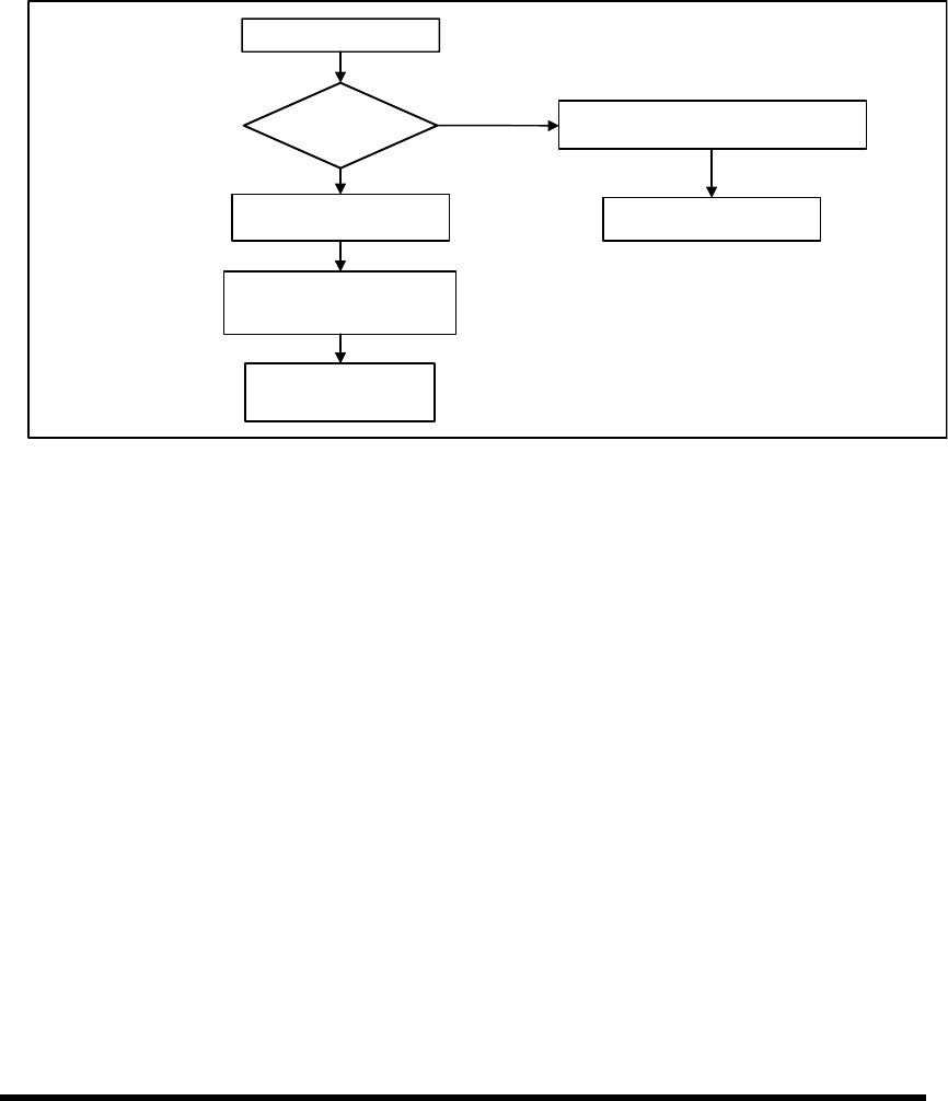
Toshiba Corporation Digital Media Network Company
Page 142 of 159
© 2004, Copyright TOSHIBA Corporation All Rights Reserved
11.9.4 Password lost
If the user password is lost and High level security is set, the drive does not allow the user to access any
data. However, the drive can be unlocked using the master password.
If the user password is lost and Maximum security level is set, it is impossible to access data. However, the
drive can be unlocked using the ERASE UNIT command with the master password. The drive will erase all
user data and unlock the drive.
User password lost
High
Level? UNLOCK with master password
Maximum
ERASE PREPARE Normal operation
ERASE UNIT
with master password
Normal operation
but data lost
Figure 5 User password lost
If both the user password and the master password are lost, the drive cannot be in normal operation mode.

Toshiba Corporation Digital Media Network Company
Page 143 of 159
© 2004, Copyright TOSHIBA Corporation All Rights Reserved
11.9.5 Command Table
This command table shows the drive’s response to commands when the Security Function is enabled.
Table 11.9-1 Security mode command actions
Command Locked mode Unlocked mode Frozen mode
CHECK POWER MODE O O O
EXECUTE DEVICE DIAGNOSTICS O O O
DEVICE CONFIGRATION X O O
DOWNLOAD MICROCODE O O O
FLUSH CACHE (EXT) X O O
FORMAT TRACK X O O
IDENTIFY DEVICE O O O
IDLE O O O
IDLE IMMEDIATE O O O
INITIALIZE DEVICE PARAMETERS O O O
NOP O O O
READ BUFFER O O O
READ DMA (EXT) X O O
READ MULTIPLE (EXT) X O O
READ NATIVE MAX ADDRESS (EXT) O O O
READ SECTORS (EXT) X O O
READ SENSE DATA O O O
READ VERIFY (EXT) X O O
RECALIBRATE O O O
SECURITY DISABLE PASSWORD X O X
SECURITY ERASE PREPARE O O O
SECURITY ERASE UNIT O O X
SECURITY FREEZE LOCK X O O
SECURITY SET PASSWORD X O X
SECURITY UNLOCK O O X
SEEK O O O
SET FEATURES O O O
SET MAX (EXT) X O O
SET MULTIPLE MODE O O O
SLEEP O O O
SMART O O O
STANDBY O O O
STANDBY IMMEDIATE O O O
WRITE BUFFER O O O
WRITE DMA (EXT) X O O
WRITE MULTIPLE (EXT) X O O
WRITE SECTORS (EXT) X O O
WRITE VERIFY X O O
O: Drive executes command normally
X: Drive rejects command with an Aborted command error

Toshiba Corporation Digital Media Network Company
Page 144 of 159
© 2004, Copyright TOSHIBA Corporation All Rights Reserved
11.10 Self-Monitoring, Analysis and Reporting Technology
Self-monitoring, analysis and reporting technology (SMART) is the function to protect user data and to
minimize the likelihood of unscheduled system downtime that may be caused by predictable degradation
and/or fault of the drive. By monitoring and storing the critical performance and calibration parameters,
SMART drives attempt to predict the likelihood of near-term degradation or fault condition. The host system
warns the user of the impending risk of data loss and advises the user of appropriate action by informing the
host system of the negative reliability .
SMART commands use a single command code and are differentiated by the value placed in the Features
register.
The Commands supported by this feature set are:
.
• SMART READ ATTRIBUTE VALUES
• SMART READ ATTRIBUTE THRESHOLDS
• SMART ENABLE/DISABLE ATTRIBUTE AUTOSAVE
• SMART SAVE ATTRIBUTE VALUE
• SMART EXECUTE OFF-LINE IMMEDIATE
• SMART READ LOG SECTOR
• SMART WRITE LOG SECTOR
• SMART ENABLE OPERATIONS
• SMART DISABLE OPERATIONS
• SMART RETURN STATUS
• SMART ENABLE/DISABLE AUTOMATIC OFF-LINE
11.10.1 Attributes
Attributes are the specific performance or calibration parameters that are used in analyzing the status of the
drive. Attributes are selected by the drive manufacturer based on that attribute’s ability to predict degrading or
faulty conditions for that particular drive. The specific set of attribute being used and the identity of these
attributes is vendor specific and proprietary.
11.10.2 Attributes values
Attribute values are used to measure the relative reliability of individual performance or calibration attributes.
11.10.3 SMART function default setting
The drives are shipped from the drive manufacturer’s factory with the SMART feature disabled. SMART
feature will be enabled by the system manufacturer or the application.

Toshiba Corporation Digital Media Network Company
Page 145 of 159
© 2004, Copyright TOSHIBA Corporation All Rights Reserved

Toshiba Corporation Digital Media Network Company
Page 146 of 159
© 2004, Copyright TOSHIBA Corporation All Rights Reserved
11.11 Adaptive Power Mode Control
Adaptive Power Mode Control is a function to reduce power consumption without performance degradation.
The drive supports the following Idle modes of 3 levels. The drive enters into idle mode adaptively in accordance
with the command pattern.
11.11.1 Performance Idle
The drive enters Performance Idle mode at the completion of a command from host. In this mode, electric
circuit and servo is ready to process the next command without delay.
11.11.2 Active Idle
Some of electric circuit and servo functions are powered off in this mode. The heads are stopped near the
disk center . If a shock is detected by Shock Sensor, the drive enters into Performance Idle mode automatically.
Power consumption for Active Idle mode is 55%∼65% lower than that of Performance Idle mode. Command
processing time is approximately 35ms longer than that of Performance Idle mode.
11.11.3 Low Power Idle
In Low Power Idle mode, the heads are unloaded on the ramp and the spindle motor continues normal rotation.
Power consumption for Low Power Idle mode is 60%∼70% lower than that of Performance Idle mode.
Command processing time is approximately 400ms longer than that of Performance Idle mode.
11.11.4 Transition time
The transition time changes dynamically in accordance with the current command pattern.
Toshiba Corporation Digital Media Network Company
Page 147 of 159
© 2004, Copyright TOSHIBA Corporation All Rights Reserved
11.12 Reset
A RESET condition sets the drive ( or both drives in case of Drive0/Drive1 connection ) BSY, allowing the
drive to perform the specified initialization required for normal operation.
A RESET condition can be generated by both hardware and software. There are two hardware resets,
one is by the Host (- RESET) and the other is by the drive power sense circuitry. These resets are set high
when the system and the drive respectively acknowledge specified supply voltage ( See 6.1).
The other reset is software generated. The Host can write to the Device Control register and set the
reset bit. The host software condition will continue until the reset bit is set to zero.
.
Once the reset is negated and the drive is re-enabled, with BSY still active, the drive will perform
necessary hardware initialization, clear any previously programmed drive parameters and revert
to the defaults, load the Task File registers with their initial values, and then clear BSY. No interrupt
is generated when initialization is complete. The initial values ( hex ) for the Task File registers are
as follows.
Table 11.12-1 Initialization of Task File registers
REGISTER POWER ON HARDWARE RESET SOFTWARE RESET
Data 00 00 00
Error 01 01 01
Sector Count 01 01 01
Sector Number 01 01 01
Cylinder Low 00 00 00
Cylinder High 00 00 00
Device/Head Register 00 00 00
Status/Alternate Status 50 or 52 50 or 52 50 or 52
Device address9 7E or FE 7E or FE 7E or FE
ECC Length 4 bytes 4 bytes no change(*1)
Data Buffer undefined undefined no change
Addressing mode default default no change
Auto stand-by mode disable disable no change
Read Cache enable enable no change (*1)
Write Cache10 enable enable no change (*1)
Multiple mode 16 sectors 16 sectors no change (*1)
DMA transfer mode Multiword
DMA mode 2 Multiword DMA mode
2 no change(*1)
PIO transfer mode PIO mode 4
flow control PIO mode 4 flow
control no change(*1)
(*1): Software reset settings are affected by set feature command.
9 ATA-2 Notes: This register is obsolete. It is recommended that a device not respond to a read of this address. If a
device does respond, it shall be sure not to drive the DD7 signal to prevent possible conflict with floppy disk
implementations.
The drive supports this register to maintain compatibility for ATA-1.
10 ATA-2 Notes: The default mode for write cache is “disable” after ATA-2. This is violation of ATA-2 specification. This setting can be
changed by factory.
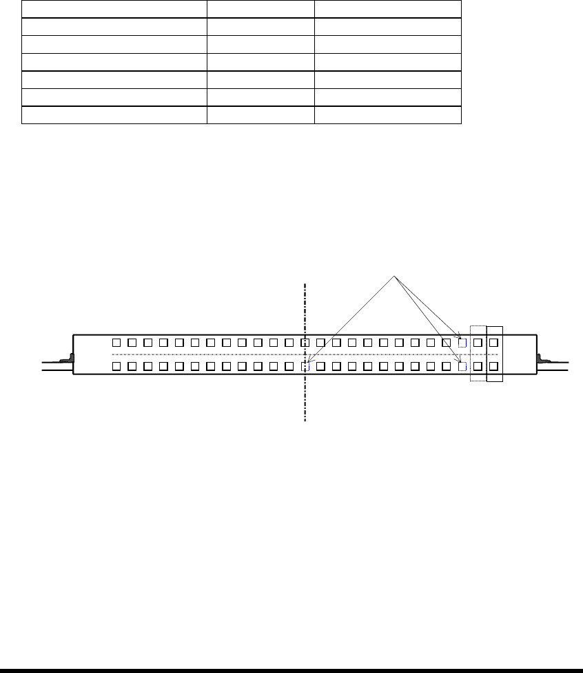
Toshiba Corporation Digital Media Network Company
Page 148 of 159
© 2004, Copyright TOSHIBA Corporation All Rights Reserved
11.13 Drive0/Drive1 Configuration
Drive address shall be set by the optional jumper of interface connector.
The drive runs as Drive0 when the jumper is open or if jumper plug is set to position B-D when
P28(CSEL) signal is low. The drive runs as Drive1 when the jumper plug is inserted into position C-D or
if jumper plug is set to position B-D when P28 (CSEL) signal is high. In case of two- drive configuration,
one shall be Drive0 and the other should be Drive1.
ATA /ATAPI specifies to use P28 with jumper plug set to position B-D. It is recommended to follow the
ATA / ATAPI specification.
Jumper P28 Drive
No Jumper - Drive0
C-D Jumper - Drive1
B-D Jumper LOW Drive0
B-D Jumper HIGH Drive1
A-B Jumper - Drive1
A-C Jumper - Prohibit
Figure 6 Optional jumper for Drive0/Drive1
Polarity key
43
44
1 C A
2 D B

Toshiba Corporation Digital Media Network Company
Page 149 of 159
© 2004, Copyright TOSHIBA Corporation All Rights Reserved
11.14 Cache Memory
11.14.1 Cache Operations
(1) READ CACHE OPERATION
Receiving a read command, the data in the buffer memory are sent to the host without access to the disk
media as long as the object data reside in the buffer memory and the conditions for the drive’s read cache
operation are fulfilled.
If any of the conditions of the read cache operation is not fulfilled, the drive carries out read data operation
and the object data for the read command is read from the media and kept in the buffer and then the data is
transferred from the buffer to the host.
The following data required by the read command may continuously be read by the buffer under the drive’s
read ahead cache operation until the buffer available for read cache is full or the new command is received.
(2) WRITE CACHE OPERATION
Receiving a write command, the drive continuously receives the write data from the host until all data are
transferred or the buffer available for write cache is full, whether the data are written on the media or not. If
all data for the command are received, the drive reports completion of the command by negating BSY bit
and issuing INTERRUPT.
If the command which follows the write cache command is also a write command for succeeding block
address, the drive receives write data from host without waiting for the previously received data to be written
on the media. And the drive reports completion of the command when the buffer receives all the data.
During a write cache operation, DASP (LED) signal line is kept “on” until all the data in the write buffer are
written on the media.
11.14.2 Notes for write cache
(1) Loss of data in write buffer
If write cache is enabled, hard reset or soft reset does not cause data loss . But power off immediate after
completion of the command may cause data loss, because actual writing of the data onto the media is not
completed at this moment. Therefore, it is recommended that any other command except write or read
command is executed and completion of the command is confirmed before powering off the drive. Stand-by
command can be helpful for this purpose.
(2) Error report
When write cache is enabled, any unrecoverable error encountered after the report of completion of a
command shall be reported by the later command. Actual writing of the data onto the media may not be
completed at this moment. In this case, READY bit is negated to show that the error has occurred during
the write cache operation previously executed.
Address validity check is performed with actual media access . The error may be reported during the
execution of a command or after completion of a write cache command if the address the data has tried to
access is non-existent.
11.15 Automatic Write Reallocation
If the drive has difficulty in executing normal write operation due to unrecoverable errors such as ID NOT
FOUND, the sectors those show some errors may be reallocated automatically to continue normal operation
and secure the write data. This operation is helpful especially in write cache, when the completion of the
command is reported before actual writing to media. During write operation including this AWRE function,
DASP signal is kept on . This operation takes 20 seconds maximum to be completed, therefore, the
time-out period should be set longer than this value. If the next command is a write command, the data of
the first block will be transferred without any delay.

Toshiba Corporation Digital Media Network Company
Page 150 of 159
© 2004, Copyright TOSHIBA Corporation All Rights Reserved
12. Protocol
Commands can be grouped into different classes according to the protocols used for command execution.
The command classes with their associated protocols are defined below.
For all commands, the host first checks BSY bit and DRDY bit. If BSY=1, the host should proceed no
further unless and until the BSY=0, and the DRDY=1.
Interrupts are cleared when host reads Status register, issues a reset, or writes to the Command register.
Interrupts are not cleared when host reads Alternate Status register.
A command shall only be interrupted with a hardware or software reset. The result of writing to the
command register while BSY=1 or DRQ=1 is unpredictable and may result in data corruption. Therefore,
a command should only be interrupted by a reset at times when the host judges that there is a problem,
such as receiving no response from a drive. Host programmers should set command time-out periods
enough long in order to avoid having effect on the device's ability to perform level retry and data recovery
activities.

Toshiba Corporation Digital Media Network Company
Page 151 of 159
© 2004, Copyright TOSHIBA Corporation All Rights Reserved
12.1 PIO data in commands
Commands for this class are:
• IDENTIFY DEVICE
• READ BUFFER
• READ SECTOR(S) (with and without retry)
• READ SECTOR(S) EXT
• READ MULTIPLE
• READ MULTIPLE EXT
• SMART Read Attribute Values
• SMART Read Attribute Thresholds
• SMART Read Log Sector
• DEVICE CONFIGRATION IDENTIFY
PIO data in protocol:
a) The host writes any required command parameters to the Features, Sector Count, Sector Number, Cylinder
High, Cylinder Low and Device/Head registers.
b) The host writes the command code to the Command register.
c) For each sector ( or block ) of data to be transferred:
1) The drive sets BSY bit and prepares to transfer a sector (or block) of data to the host.
2) When a sector (or block) of data is available for transfer to the host, the drive sets the DRQ bit and clears
the BSY bit and asserts INTRQ.
3) After detecting INTRQ, the host reads the contents of the Status register.
4) The drive negates INTRQ in response to the Status register being read.
5) The host reads a sector (or block) of data via the Data register.
6) In response to a sector (or block) of data being transferred, the drive clears the DRQ bit.
The Read Multiple command transfers one block ( the number of sectors defined by the Set Multiple
command ) of data for each interrupt. The other commands transfer one sector of data for each interrupt.
If the drive detects an invalid parameter in register setting, the drive clears BSY bit and sets the ERR bit in
the Status register and sets ABRT bit in the Error register and asserts INTRQ in order to terminate the
command execution.
If an uncorrectable error occurs, the drive will set DRQ bit and clear BSY bit and set ERR bit and stores the
error status in Error register and address the information of the error sector to Sector Number, Cylinder
High, Cylinder Low and Device/Head registers and asserts INTRQ.
If uncorrectable data error ( the UNC is set ) occurs, the drive will transfer a sector of the defective data to
the host. If the others error occur, the contents of the data to be transferred shall not be ensured. In both
cases, the host should complete transfer of the sector of data in response to INTRQ being asserted. In case
of Read Multiple command, the host should complete transfer of a block of data which includes the sector
with defective data.

Toshiba Corporation Digital Media Network Company
Page 152 of 159
© 2004, Copyright TOSHIBA Corporation All Rights Reserved
12.2 PIO data out commands
Commands for this class are:
• (FORMAT TRACK)
• WRITE BUFFER
• WRITE MULTIPLE
• WRITE MULTIPLE EXT
• WRITE SECTOR(S) (with and without retry)
• WRITE SECTOR(S) EXT
• WRITE VERIFY
• SECURITY DISABLE PASSWORD
• SECURITY ERASE UNIT
• SECURITY SET PASSWORD
• SECURITY UNLOCK
• SET MAX SET PASSWORD
• SMART Write Log Sector
• DOWNLOAD MICROCODE
PIO data out protocol:
a) The host writes any required command parameters to the Features, Sector Count, Sector Number, Cylinder
High, Cylinder Low and Device/Head registers.
b) The host writes the command code to the Command register.
c) The drive sets the BSY bit .
d) For each sector (or block) of data to be transferred:
1) When the drive is ready to receive a sector (or block) of data from the host, it sets the DRQ bit and clears
the BSY bit.
2) The host writes a sector (or block) of data via the Data Register.
3) After receiving the sector (or block) , the drive clears the DRQ bit and sets the BSY bit.
4) When the drive has finished processing the sector (or block) , it sets the DRQ bit and clears the BSY bit
and asserts INTRQ.
5) After detecting INTRQ, the host reads the Status register.
6) The drive negates INTRQ in response to the Status register being read.
The drive negates INTRQ in response to the Status register being read.

Toshiba Corporation Digital Media Network Company
Page 153 of 159
© 2004, Copyright TOSHIBA Corporation All Rights Reserved
The Write Multiple command transfers one block ( the number of sectors is defined by the Set Multiple
command ) of data for each interrupt. The other commands transfer one sector of data for each interrupt.
If the drive detects an invalid parameter in register setting, the drive clears the BSY bit and sets the ERR bit
in the Status register and sets the ABRT bit in the Error register and asserts INTRQ to terminate the
command execution.
If an unrecoverable error occurs, the drive sets the DRQ bit and clears the BSY bit and sets the ERR bit and
stores the error status in Error register and report the address information of the sector with error to Sector
Number, Cylinder High, Cylinder Low and Device/Head registers and asserts INTRQ.
12.3 Non-data commands
Commands for this class are:
• CHECK POWER MODE
• EXECUTE DEVICE DIAGNOSTICS
• FLUSH CACHE
• FLUSH CACHE EXT
• IDLE
• IDLE IMMEDIATE
• INITIALIZE DEVICE PARAMETERS
• NOP
• READ VERIFY SECTOR(S)
• READ VERIFY SECTOR(S) EXT
• READ NATIVE MAX ADDRESS
• READ NATIVE MAX ADDRESS EXT
• RECALIBRATE
• SEEK
• SET FEATURES
• SET MULTIPLE MODE
• SLEEP
• STANDBY
• STANDBY IMMEDIATE
• SECURITY ERASE PREPARE
• SECURITY FREEZE LOCK
• SMART Enable/Disable Attribute Autosave
• SMART Save Attribute Values
• SMART Executive Off-line Immediate
• SMART Enable Operation
• SMART Disable Operation
• SMART Return Status
• SMART Enable/Disable Automatic Off-line
• SET MAX ADDRESS
• SET MAX ADDRESS EXT
• SET MAX LOCK
• SET MAX UNLOCK
• SET MAX FREEZE LOCK
• DEVICE CONFIGRATION RESTORE
• DEVICE CONFIGRATION FREEZE LOCK
• DEVICE CONFIGRATION SET
• READ SENCE DATA

Toshiba Corporation Digital Media Network Company
Page 154 of 159
© 2004, Copyright TOSHIBA Corporation All Rights Reserved
Non-data protocol:
a) The host writes any required command parameters to the Features, Sector Count, Sector Number, Cylinder
High, Cylinder Low and Device/Head registers.
b) The host writes the command code to the Command register.
c) The drive sets the BSY bit .
d) When the drive has finished processing a sector (or block) of data, it clears the BSY bit and asserts INTRQ.
e) In response to the INTRQ, the host reads the Status register.
f) The drive negates INTRQ in response to the Status register being read
See each command description for error report protocol.

Toshiba Corporation Digital Media Network Company
Page 155 of 159
© 2004, Copyright TOSHIBA Corporation All Rights Reserved
12.4 DMA data transfer commands
Commands for this class are:
• READ DMA (with and without retry)
• READ DMA EXT
• WRITE DMA (with and without retry)
• WRITE DMA EXT
Data transfers using DMA commands differ in two ways from PIO transfers:
data transfers are performed using the DMA channel
the drive issues only one interrupt at the completion of each command
Initiation of the DMA transfer commands is identical to the READ SECTOR(S) or WRITE SECTOR(S)
commands except that the host initializes the DMA channel prior to issuing the command.
The interrupt handler for DMA transfers is different in that no intermediate sector interrupts are issued on
multi-sector transfer but issued only once at the completion of each command.
DMA data transfer protocol:
a) Host initializes the DMA channel.
b) Host writes any required command parameters to the Features, Sector Count, Sector Number, Cylinder High,
Cylinder Low and Device/Head registers.
c) Host writes the command code to the Command register.
d) The drive sets the BSY bit .
e) The drive sets DMARQ, when it is ready to transfer data.
f) Host transfers the data using DMA transfer mode set by the Set Features command .
g) When all of the data has been transferred, the drive issues INTRQ.
h) The host resets the DMA channel.
i) After detecting INTRQ, the host reads the Status register.
j) The drive negates INTRQ in response to the Status register being read.

Toshiba Corporation Digital Media Network Company
Page 156 of 159
© 2004, Copyright TOSHIBA Corporation All Rights Reserved
12.5 Ultra DMA
Ultra DMA protocol is used with Read DMA, and Write DMA commands. Ultra DMA modes are set by Set
features command. Since the setting after power-up ( Default setting ) is mode 2 of Multi Word DMA, Set
Features command shall be issued to be used in Ultra DMA mode.
An Ultra DMA data transfer is accomplished through a series of Ultra DMA data in or data out bursts. Each
Ultra DMA burst has three mandatory phases of operation: the initiation phase, the data transfer phase, and
the Ultra DMA burst termination phase. An Ultra DMA burst is defined as the period from an assertion of
DMACK- by the host to the subsequent negation of DMACK-. A recipient shall be prepared to receive at
least 2 data words.
Both the host and drive perform a CRC function during an Ultra DMA burst. At the end of an Ultra DMA
burst, the drive compares its CRC data to the data sent from the host. The drive requires an Ultra DMA
burst termination for each sector to compare CRC data to the data sent from the host.
1. Initiation phase
a) An Ultra DMA burst initiation phase begins with the assertion of DMARQ by the drive and ends when the
sender generates a STROBE edge to transfer the first data word.
b) An Ultra DMA burst is always requested by a drive asserting DMARQ.
c) A host indicates it is ready to initiate the requested Ultra DMA burst by asserting DMACK-.
d) A host shall never assert DMACK- without first detecting that DMARQ is asserted.
e) For Ultra DMA data in bursts: a drive may begin driving DD(15:0) after detecting that DMACK- is
asserted, STOP negated, and HDMARDY- is asserted.
f) After asserting DMARQ or asserting DDMARDY- for an Ultra DMA data out burst, the shall not negate
either signal until the first STROBE edge is generated.
g) After negating STOP or asserting HDMARDY- for an Ultra DMA data in burst, a host shall not change the
state of either signal until the first STROBE edge is generated.
2. Data transfer phase
a) The data transfer phase is in effect from after Ultra DMA burst initiation until Ultra DMA burst termination.
b) A recipient pauses an Ultra DMA burst by negating DMRDY- and resumes an Ultra DMA burst by
reasserting DMARDY-.
c) A sender pauses an Ultra DMA burst by not generating STROBE edges and resumes by generating
STROBE edges.
d) A recipient must not signal a termination request when a sender stops generating STROBE edges. In the
absence of a termination from the sender, the recipient should always negate DMARDY- and wait the
required period before signaling a termination request.
e) A sender may generate STROBE edges at greater than the minimum period specified by the enabled
Ultra DMA Mode . The sender should not generate STROBE edges at less than the minimum period
specified by the abled Ultra DMA Mode. A recipient should be able to receive data at the minimum
period specified by the enabled Ultra DMA Mode.

Toshiba Corporation Digital Media Network Company
Page 157 of 159
© 2004, Copyright TOSHIBA Corporation All Rights Reserved
3. Ultra DMA burst termination phase
a) Either a sender or a recipient may terminate an Ultra DMA burst.
b) Ultra DMA burst termination is not the same as command termination or completion. If an Ultra DMA
burst termination occurs before the command is complete, the command shall be completed by
initiation of a new Ultra DMA burst at some later time or aborted by the host issuing a hardware or
software reset to the drive.
c) An Ultra DMA shall be paused before a recipient requests a termination.
d) A host requests a termination by asserting STOP. A drive acknowledges a termination request by
negating DMARQ.
e) A drive requests a termination by negating DMARQ. A host acknowledges a termination request by
asserting STOP.
f) Once a sender requests a termination, it does not change the state of STROBE until the recipient
acknowledges the request. Then, if STROBE is not the asserted state, the sender returns STROBE to
the asserted state. No data shall be transferred on this transition of STROBE.
g) A sender returns STROBE to the asserted state whenever it detects a termination request from the
recipient. No data shall be transferred nor CRC calculated on this edge of DSTROBE.
h) Once a recipient requests a termination, it does not change DMARDY from the negated state for the
remainder of an Ultra DMA burst.
k) A recipient ignores a STROBE edge when DMARQ is negated or STOP is asserted.
CRC
Both the host and drive perform a CRC function during an Ultra DMA burst. the host and drive use 4ABAh
as an initial value. The host and the drive calculate CRC value during each STROBE edge of data transfer
using current value of CRC and transferred data with CRC polynomial. CRC function is not performed after
an Ultra DMA burst completion of STROBE set. At the completion of an Ultra DMA burst, the host reports
the CRC data on data bus and negates DMACK- to pass the result to the drive.
The drive compares the CRC data sent from the host. If the two values do not match, the drive reports an
error after at the end of the command. The generative polynomial for CRC is :
( X ) = X 16 + X 12 + X 5 + 1
The following figure shows an example of CRC generative logic ( ATA / ATAPI-6 )
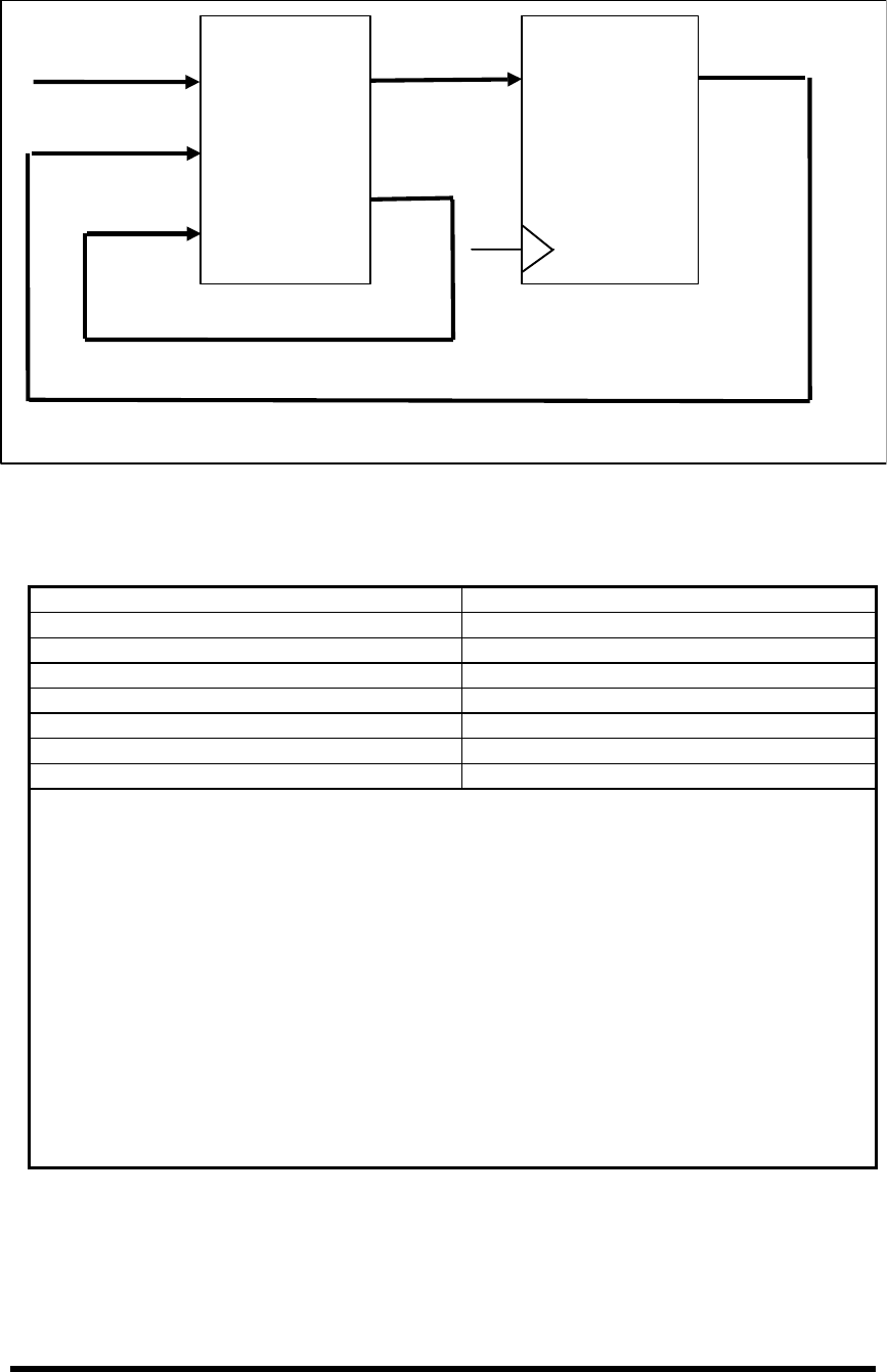
Toshiba Corporation Digital Media Network Company
Page 158 of 159
© 2004, Copyright TOSHIBA Corporation All Rights Reserved
Combinational
Logic Edge
Triggered
Register
Device
CRCOUT (15:0)
CRCIN (15:0:)DD(15:0)
f1-f16
Word
Clock
CRCIN0 = f16 CRCIN8 = f8 XOR f13
CRCIN1 = f15 CRCIN9 = f7 XOR f12
CRCIN2 = f14 CRCIN10 = f6 XOR f11
CRCIN3 = f13 CRCIN11 = f5 XOR f10
CRCIN4 = f12 CRCIN12 = f4 XOR f9 XOR f16
CRCIN5 = f11 XOR f16 CRCIN13 = f3 XOR f8 XOR f15
CRCIN6 = f10 XOR f15 CRCIN14 = f2 XOR f7 XOR f14
CRCIN7 = f9 XOR f14 CRCIN15 = f1 XOR f6 XOR f13
f1 = DD0 XOR CRCOUT15 f9 = DD8 XOR CRCOUT7 XOR f5
f2 = DD1 XOR CRCOUT14 f10 = DD9 XOR CRCOUT6 XOR f6
f3 = DD2 XOR CRCOUT13 f11 = DD10 XOR CRCOUT5 XOR f7
f4 = DD3 XOR CRCOUT12 f12 = DD11 XOR CRCOUT4 XOR f1 XOR f8
f5 = DD4 XOR CRCOUT11 XOR f1 f13 = DD12 XOR CRCOUT3 XOR f2 XOR f9
f6 = DD5 XOR CRCOUT10 XOR f2 f14 = DD13 XOR CRCOUT2 XOR f3 XOR f10
f7 = DD6 XOR CRCOUT9 XOR f3 f15 = DD14 XOR CRCOUT1 XOR f4 XOR f11
f8 = DD7 XOR CRCOUT8 XOR f4 f16 = DD15 XOR CRCOUT0 XOR f5 XOR f12
Notes:
1) f = feedback
2) DD = Data to or from the bus
3) CRCOUT = 16-bit edge triggered result (current CRC)
4) CRCOUT(15:0) are sent on matching order bits of DD(15:0)
5) CRCIN = Output of combinatorial logic (next CRC)

Toshiba Corporation Digital Media Network Company
Page 159 of 159
© 2004, Copyright TOSHIBA Corporation All Rights Reserved
12.6 Other timings
See HOST INTERFACE section for timings which are not shown here.
Table 12.6-1 Other timings.
Function and Intervals Timeout
• POWER ON TIMINGS
From power on to BSY=1 400 ns maximum
From Power on to BSY=0, DRDY=1 31 s maximum
• SOFT RESET TIMINGS
From soft reset assertion (SRST=1) to BSY=1 400 ns maximum
From soft reset negation (SRST=0) to drive ready (BSY=0, DRDY=1) 10 sec maximum
• HARD RESET TIMINGS
From hard reset assertion to BSY=1 400 ns maximum
From hard reset negation to drive ready (BSY=0, DRDY=1) 31 sec maximum
• DATA IN COMMANDS
From writing to command register to BSY=1 400 ns maximum
From BSY=1 to BSY=0, DRQ=1, INTRQ set (When the drive is in idle mode) 20 sec maximum
From BSY=1 to BSY=0, DRQ=1, INTRQ set (When the drive is in standby mode) 35 sec maximum
Drive Busy during data transfer 5 µs minimum
• DATA OUT COMMANDS
From writing to command register to BSY=1 400 ns maximum
From BSY=1 to BSY=0, DRQ=1 700 µs(*1) maximum
Drive Busy during data transfer 5 µs minimum
From BSY=1 to INTRQ set (When the drive is in idle mode) 10 sec maximum
From BSY=1 to INTRQ set (When the drive is in standby mode) 25 sec maximum
• NON-DATA COMMANDS
From writing to command register to BSY=1 400 ns maximum
From BSY=1 to INTRQ set (When the drive is in standby mode) 17 sec maximum
• DMA DATA TRANSFER COMMANDS
From writing to command register to BSY=1 400 ns maximum
(*1) When the following commands are issued by the host as First Command after hardware reset, the command’s
time-out value of the field is 10 seconds.
Security Diable Password
Security Erase Unit
Security Set Password
Security Unlock
