TransCore 2000B Vehicle Reporting System User Manual LEON G100 LEON G200
TransCore Vehicle Reporting System LEON G100 LEON G200
UserManual.wiki
>
TransCore
>
2000B User Manual
>
User Manual I
Contents
1.
User Manual I
2.
User Manual II
User Manual I
Navigation menu
Upload a User Manual
Namespaces
Wiki Guide
HTML
PDF
Info
Views
User Manual
Discussion / Help
Navigation
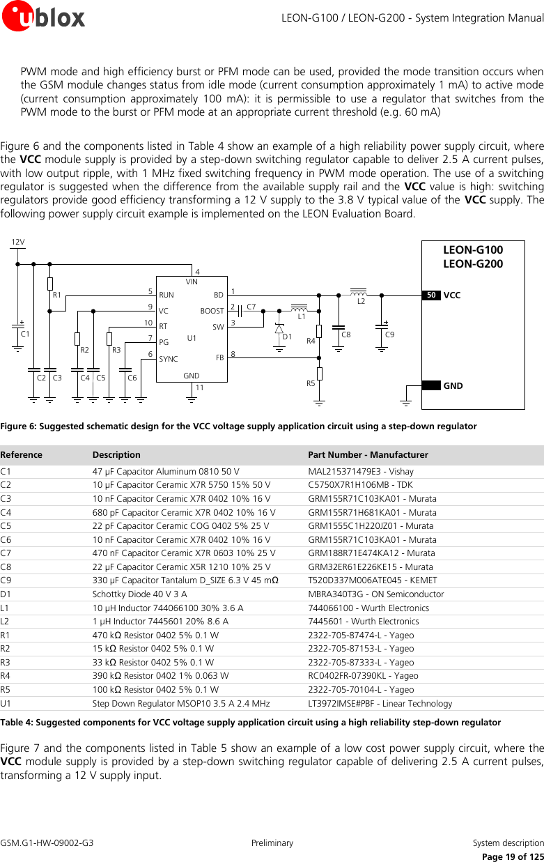
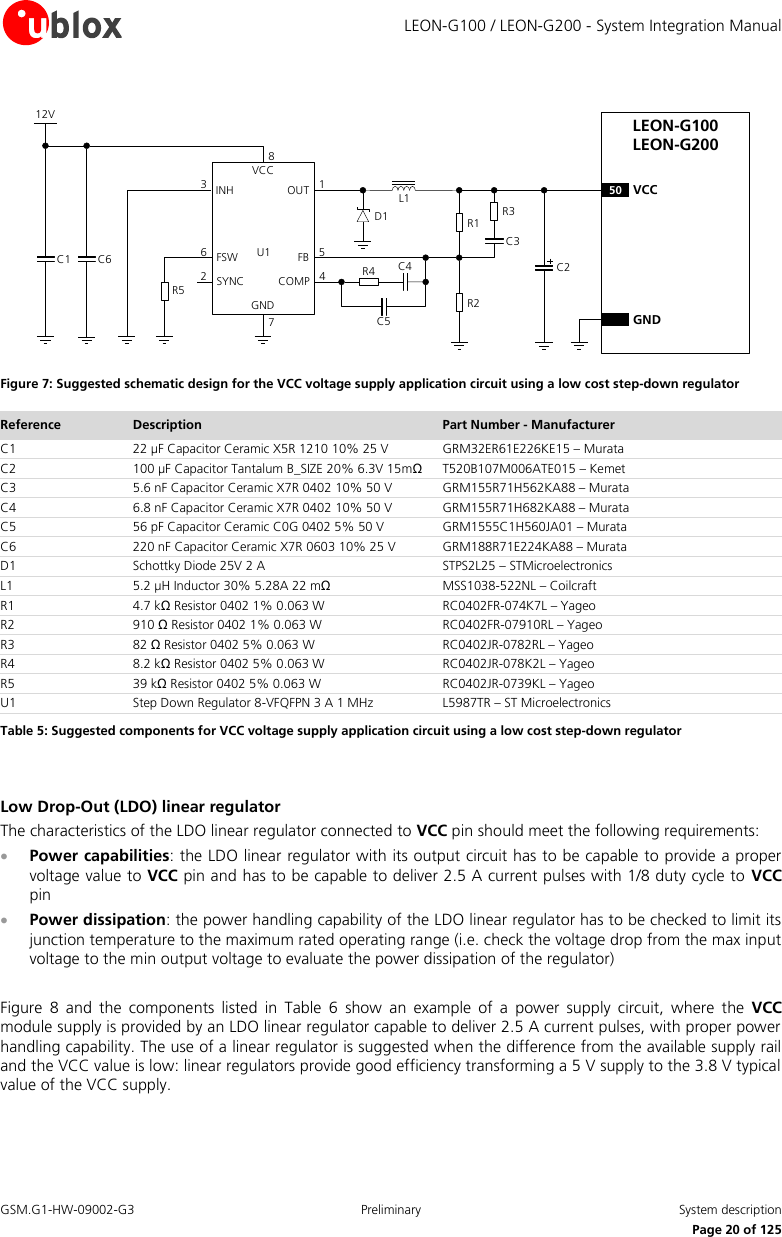
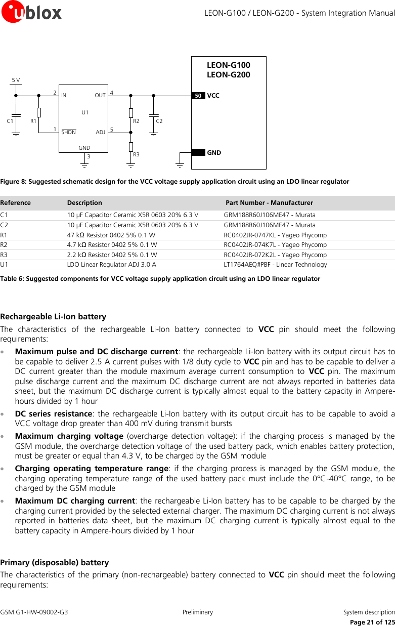
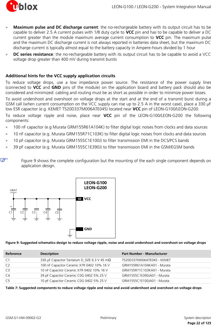
![LEON-G100 / LEON-G200 - System Integration Manual GSM.G1-HW-09002-G3 Preliminary System description Page 13 of 125 1.4 Operating modes LEON-G100/LEON-G200 modules include several operating modes, each have different features and interfaces. Table 2 summarizes the various operating modes and provides general guidelines for operation. Operating Mode Description Features / Remarks Transition condition General Status: Power-down Not-Powered Mode VCC supply not present or below normal operating range. Microprocessor switched off (not operating). RTC only operates if supplied through V_BCKP pin. Module is switched off. Application interfaces are not accessible. Internal RTC timer operates only if a valid voltage is applied to V_BCKP pin. Any external signal connected to the UART I/F, I2S I/F, HS_DET, GPIOs must be tristated to avoid an increase of module power-off consumption. Module cannot be switched on by a falling edge provided on the PWR_ON input, neither by a preset RTC alarm, nor by charger detection on the V_CHARGE and CHARGE_SENSE pins. Power-Off Mode VCC supply within normal operating range. Microprocessor not operating. Only RTC runs. Module is switched off: normal shutdown after sending the AT+CPWROFF command (refer to u-blox AT Commands Manual [2]). Application interfaces are not accessible. Only internal RTC timer in operation. Any external signal connected to the UART I/F, I2S I/F, HS_DET, GPIOs must be tristated to avoid an increase of the module power-off consumption. Module can be switched on by a falling edge provided on the PWR_ON input, by a preset RTC alarm, or by charger detection on the V_CHARGE and CHARGE_SENSE pins. General Status: Normal Operation Idle-Mode Microprocessor runs with 32 kHz as reference oscillator. Module does not accept data signals from an external device. If power saving is enabled, the module automatically enters idle mode whenever possible. If hardware flow control is enabled, the CTS line indicates that the module is in active-mode and the UART interface is enabled: the line is driven in the OFF state when the module is not prepared to accept data by the UART interface. If hardware flow control is disabled, the CTS line is fixed to ON state. Module by default is not set to automatically enter idle mode whenever possible, unless power saving configuration is enabled by appropriate AT command (refer to u-blox AT Commands Manual [2], AT+UPSV). If the module is registered with the network and power saving is enabled, it automatically enters idle mode and periodically wakes up to active mode to monitor the paging channel for the paging block reception according to network indication. If module is not registered with the network and power saving is enabled, it automatically enters idle mode and periodically wakes up to monitor external activity. Module wakes up from idle-mode to active-mode for an incoming voice or data call. Module wakes up from idle mode to active mode if an RTC alarm occurs. Module wakes up from idle mode to active mode when data is received on UART interface (refer to 1.9.1 section). Module wakes up from idle mode to active mode when the RTS input line is set to the ON state by the DTE if the AT+UPSV=2 command is sent to the module (refer to 1.9.1 section). Active-Mode Microprocessor runs with 26 MHz as reference oscillator. The module is ready to accept data signals from an external device. Module is switched on and is fully active: power saving is not enabled. The application interfaces are enabled. If power saving is enabled, the module automatically enters idle mode whenever possible.](https://usermanual.wiki/TransCore/2000B.User-Manual-I/User-Guide-2324779-Page-13.png)
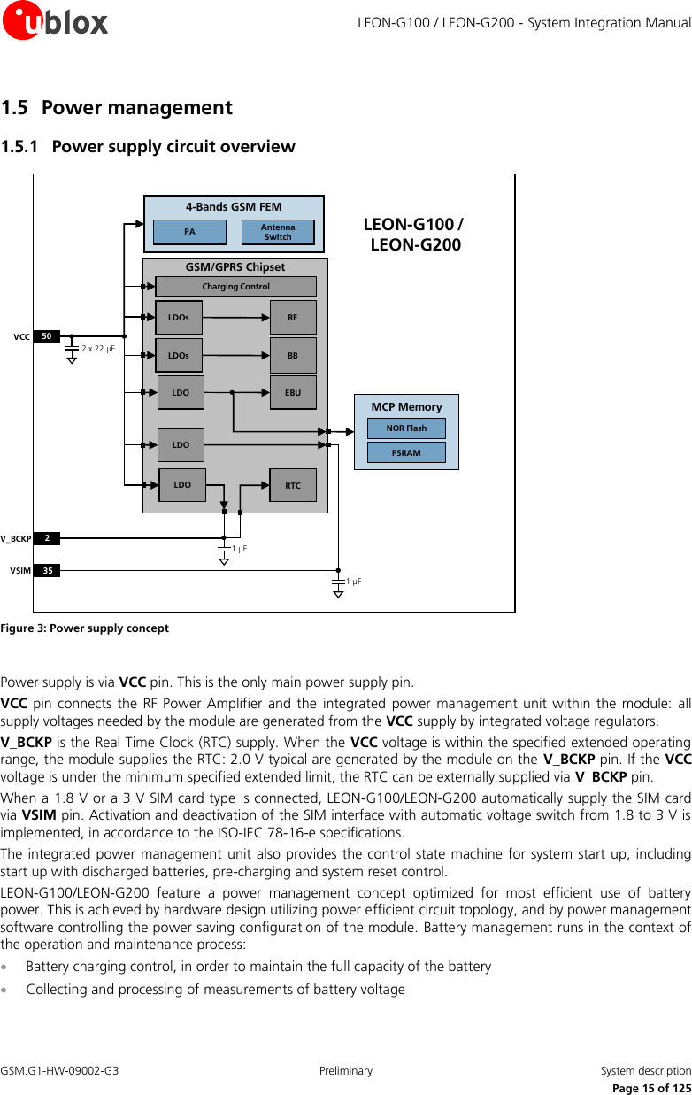
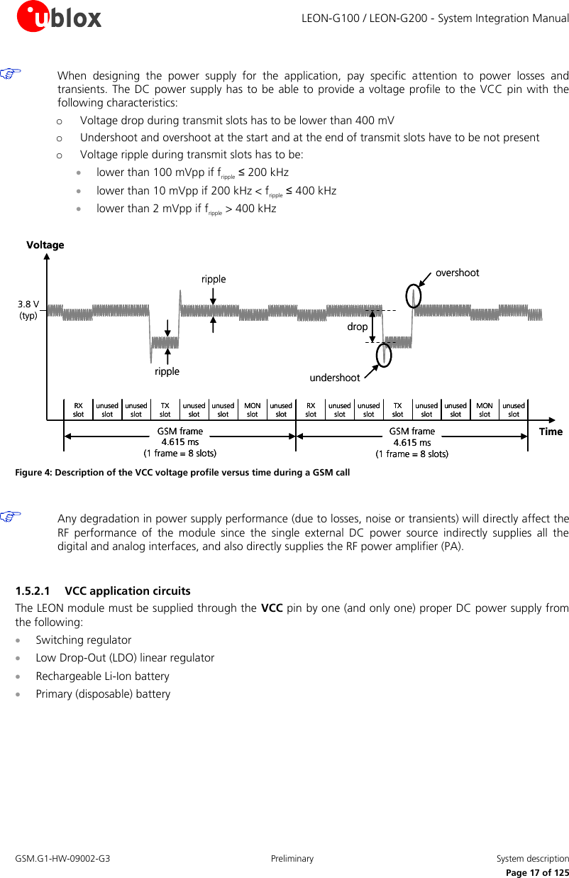
![LEON-G100 / LEON-G200 - System Integration Manual GSM.G1-HW-09002-G3 Preliminary System description Page 16 of 125 1.5.2 Module supply (VCC) LEON-G100/LEON-G200 modules must be supplied through VCC pin by a DC power supply. Voltages must be stable, due to the surging consumption profile of the GSM system (described in the section 1.5.3). Name Description Remarks VCC Module Supply Clean and stable supply is required: low ripple and low voltage drop must be guaranteed. Voltage provided has to be always above the minimum limit of the operating range. Consider that there are large current spike in connected mode, when a GSM call is enabled. GND Ground GND pins are internally connected but good (low impedance) external ground can improve RF performances: all GND pins must be externally connected to ground. Table 3: Module supply pins VCC pin ESD sensitivity rating is 1 kV (HBM JESD22-A114F). A higher protection level could be required if the line is externally accessible on the application board. A higher protection level can be achieved mounting an ESD protection (e.g. EPCOS CA05P4S14THSG varistor array) on the line connected to this pin if it is externally accessible on the application board. The voltage provided to VCC pin must be within the normal operating range limits specified in the LEON-G100 / LEON-G200 Data Sheet [1]. Complete functionality of the module is only guaranteed within the specified operational normal voltage range. The module cannot be switched on if the VCC voltage value is below the specified normal operating range minimum limit: ensure that the input voltage at VCC pin is above the minimum limit of the normal operating range for more than 1 second after the start of the switch-on of the module. When LEON-G100/LEON-G200 modules are in operation, the voltage provided to VCC pin can exceed the normal operating range limits but must be within the extended operating range limits specified in LEON-G100/LEON-G200 Data Sheet [1]. Module reliability is only guaranteed within the specified operational extended voltage range. The module switches off when VCC voltage value drops below the specified extended operating range minimum limit: ensure that the input voltage at VCC pin never drops below the minimum limit of the extended operating range when the module is switched on, not even during a GSM transmit burst, where the current consumption can rise up to maximum peaks of 2.5 A in case of a mismatched antenna load. Operation above the extended operating range maximum limit is not recommended and extended exposure beyond it may affect device reliability. Stress beyond the VCC absolute maximum ratings may cause permanent damage to the module: if necessary, voltage spikes beyond VCC absolute maximum ratings must be limited to values within the specified boundaries by using appropriate protection.](https://usermanual.wiki/TransCore/2000B.User-Manual-I/User-Guide-2324779-Page-16.png)
![LEON-G100 / LEON-G200 - System Integration Manual GSM.G1-HW-09002-G3 Preliminary System description Page 23 of 125 1.5.3 Current consumption profiles During operation, the current consumed by LEON-G100/LEON-G200 through VCC pin can vary by several orders of magnitude. This is applied to ranges from the high peak of current consumption during the GSM transmitting bursts at maximum power level in connected mode, to the low current consumption in idle mode when power saving configuration is enabled. 1.5.3.1 Current consumption profiles – Connected mode When a GSM call is established, the VCC consumption is determined by the current consumption profile typical of the GSM transmitting and receiving bursts. The current consumption peak during a transmission slot is strictly dependent on the transmitted power, which is regulated by the network. If the module transmits in GSM talk mode in the GSM 850 or in the EGSM 900 band at the maximum power control level (32.2 dBm typical transmitted power in the transmit slot/burst), the current consumption can reach up to 2500 mA (with highly unmatched antenna) for 576.9 µs (width of the transmit slot/burst) with a periodicity of 4.615 ms (width of 1 frame = 8 slots/bursts), so with a 1/8 duty cycle, according to GSM TDMA. During a GSM call, current consumption is in the order of 100-200 mA in receiving or in monitor bursts and is about 30-50 mA in the inactive unused bursts (low current period). The more relevant contribution to determine the average current consumption is set by the transmitted power in the transmit slot. Figure 10 shows an example of current consumption profile of the data module in GSM talk mode. Time [ms]RX slotunused slotunused slotTX slotunused slotunused slotMON slotunused slotRX slotunused slotunused slotTX slotunused slotunused slotMON slotunused slotGSM frame 4.615 ms (1 frame = 8 slots)Current [A]200 mA ~170 mA2500 mAPeak current depends on TX powerGSM frame 4.615 ms (1 frame = 8 slots)1.51.00.50.02.52.0~170 mA ~40 mA Figure 10: Description of the VCC current consumption profile versus time during a GSM call (1 TX slot) When a GPRS connection is established there is a different VCC current consumption profile also determined by the transmitting and receiving bursts. In contrast to a GSM call, during a GPRS connection more than one slot can be used to transmit and/or more than one slot can be used to receive. The transmitted power depends on network conditions and sets the peak of current consumption, but following the GPRS specifications the maximum transmitted power can be reduced if more than one slot is used to transmit, so the maximum peak of current consumption is not as high as can be the case in a GSM call. If the module transmits in GPRS class 10 connected mode in the GSM 850 or in the EGSM 900 band at the maximum power control level (30.5 dBm typical transmitted power in the transmit slot/burst), the current consumption can reach up to 1800 mA (with highly unmatched antenna) for 1.154 ms (width of the 2 transmit](https://usermanual.wiki/TransCore/2000B.User-Manual-I/User-Guide-2324779-Page-23.png)
![LEON-G100 / LEON-G200 - System Integration Manual GSM.G1-HW-09002-G3 Preliminary System description Page 24 of 125 slots/bursts) with a periodicity of 4.615 ms (width of 1 frame = 8 slots/bursts), so with a 1/4 duty cycle, according to GSM TDMA. In the following figure is reported the current consumption profiles with 2 slots used to transmit. Time [ms]RX slotunused slotunused slotTX slotTX slotunused slotMON slotunused slotRX slotunused slotunused slotTX slotTX slotunused slotMON slotunused slotGSM frame 4.615 ms (1 frame = 8 slots)Current [A]200mA ~170 mA1800 mAPeak current depends on TX power~170 mAGSM frame 4.615 ms (1 frame = 8 slots)1.51.00.50.02.52.0~40 mA Figure 11: Description of the VCC current consumption profile versus time during a GPRS connection (2 TX slots) 1.5.3.2 Current consumption profiles – Cyclic idle/active mode (power saving enabled) The power saving configuration is by default disabled, but it can be enabled using the appropriate AT command (refer to u-blox AT Commands Manual [2], AT+UPSV command). When the power saving is enabled, the module automatically enters idle-mode whenever possible. When power saving is enabled, the module is registered or attached to a network and a voice or data call is not enabled, the module automatically enters idle-mode whenever possible, but it must periodically monitor the paging channel of the current base station (paging block reception), in accordance to GSM system requirements. When the module monitors the paging channel, it wakes up to active mode, to enable the reception of paging block. In between, the module switches to idle-mode. This is known as GSM discontinuous reception (DRX). The module processor core is activated during the paging block reception, and automatically switches its reference clock frequency from the 32 kHz used in idle-mode to the 26 MHz used in active-mode. The time period between two paging block receptions is defined by the network. It can vary from 470.76 ms (width of 2 GSM multiframes = 2 x 51 GSM frames = 2 x 51 x 4.615 ms) up to 2118.42 ms (width of 9 GSM multiframes = 9 x 51 frames = 9 x 51 x 4.615 ms): this is the paging period parameter, fixed by the base station through broadcast channel sent to all users on the same serving cell. An example of the current consumption profile of the data module when power saving is enabled is shown in Figure 12: the module is registered with the network, automatically goes into idle mode and periodically wakes up to active mode to monitor the paging channel for paging block reception (cyclic idle/active mode).](https://usermanual.wiki/TransCore/2000B.User-Manual-I/User-Guide-2324779-Page-24.png)
![LEON-G100 / LEON-G200 - System Integration Manual GSM.G1-HW-09002-G3 Preliminary System description Page 25 of 125 ~30 msIDLE MODE ACTIVE MODE IDLE MODE500-700 µA 8-10 mA 20-22 mA~150 mAActive Mode EnabledIdle Mode EnabledPLL EnabledRX Enabled500-700 µA~150 mA0.44-2.09 sIDLE MODE~30 msACTIVE MODETime [s]Current [mA]150100500Time [ms]Current [mA]15010050038-40 mADSP Enabled Figure 12: Description of the VCC current consumption profile versus time when power saving is enabled: the module is in idle mode and periodically wakes up to active mode to monitor the paging channel for paging block reception 1.5.3.3 Current consumption profiles – Fixed active mode (power saving disabled) Power saving configuration is by default disabled, or it can be disabled using the appropriate AT command (refer to u-blox AT Commands Manual [2], AT+UPSV command). When power saving is disabled, the module doesn’t automatically enter idle-mode whenever possible: the module remains in active mode. The module processor core is activated during active-mode, and the 26 MHz reference clock frequency is used. An example of the current consumption profile of the data module when power saving is disabled is shown in Figure 13: the module is registered with the network, active-mode is maintained, and the receiver and the DSP are periodically activated to monitor the paging channel for paging block reception.](https://usermanual.wiki/TransCore/2000B.User-Manual-I/User-Guide-2324779-Page-25.png)
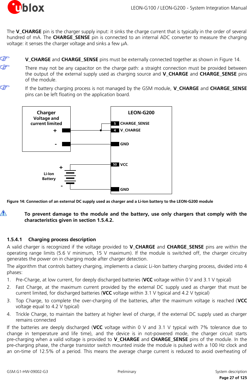
![LEON-G100 / LEON-G200 - System Integration Manual GSM.G1-HW-09002-G3 Preliminary System description Page 26 of 125 ACTIVE MODE20-22 mA 20-22 mA20-22 mA~150 mA0.47-2.12 sPaging periodTime [s]Current [mA]150100500Time [ms]Current [mA]150100500RX EnabledDSP Enabled~150 mA38-40 mA Figure 13: Description of the VCC current consumption profile versus time when power saving is disabled: active-mode is always held, and the receiver and the DSP are periodically activated to monitor the paging channel for paging block reception 1.5.4 Battery charger (LEON-G200 only) For battery charging functionalities the module is provided with integrated circuitry and software. Two pins are available to connect the positive pole of the external DC supply used as charger. Name Description Remarks V_CHARGE Charger Voltage Supply Input V_CHARGE and CHARGE_SENSE pins must be externally connected together. CHARGE_SENSE Charger Voltage Measurement Input V_CHARGE and CHARGE_SENSE pins must be externally connected together. Table 8: Battery charger pins V_CHARGE and CHARGE_SENSE pins ESD sensitivity rating is 1 kV (HBM JESD22-A114F). A higher protection level could be required if the lines are externally accessible on the application board. A higher protection level can be achieved mounting an ESD protection (e.g. EPCOS CA05P4S14THSG varistor array) on the lines connected to these pins if they are externally accessible on the application board.](https://usermanual.wiki/TransCore/2000B.User-Manual-I/User-Guide-2324779-Page-26.png)
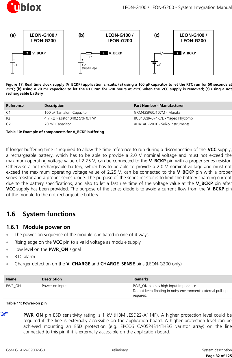
![LEON-G100 / LEON-G200 - System Integration Manual GSM.G1-HW-09002-G3 Preliminary System description Page 31 of 125 1.5.5 RTC Supply (V_BCKP) V_BCKP connects the Real Time Clock (RTC) supply, generated internally by a linear regulator integrated in the module chipset. The output of this linear regulator is enabled when the main voltage supply providing the module through VCC is within the valid operating range, or if the module is switched-off. Name Description Remarks V_BCKP Real Time Clock supply V_BCKP = 2.0 V (typical) generated by the module to supply Real Time Clock when VCC supply voltage is within valid operating range. Table 9: Real Time Clock supply pin V_BCKP pin ESD sensitivity rating is 1 kV (HBM JESD22-A114F). A higher protection level could be required if the line is externally accessible on the application board. A higher protection level can be achieved by mounting an ESD protection (e.g. EPCOS CA05P4S14THSG varistor array) on the line connected to this pin if it is externally accessible on the application board. The RTC provides the time reference (date and time) of the module, also in power-off mode, since the RTC runs when the V_BCKP voltage is within its valid range (specified in LEON-G100 / LEON-G200 Data Sheet [1]). The RTC block is able to provide programmable alarm functions by means of the internal 32.768 kHz clock. The RTC block has very low, but highly temperature dependent power consumption. For example at 25°C and a V_BCKP voltage of 2.0 V the power consumption is approximately 2 µA, whereas at 85°C and an equal voltage it increases to 5 µA. The RTC can be supplied from an external back-up battery through V_BCKP, when the main voltage supply is not provided to the module through VCC. This enables the time reference (date and time) to run even when the main supply is not provided to the module. The module cannot switch on if a valid voltage is not present on VCC, even when RTC is supplied through V_BCKP (meaning that VCC is mandatory to switch-on the module). If V_BCKP is left unconnected and the main voltage supply of the module is removed from VCC, the RTC is supplied from the 1 µF buffer capacitor mounted inside the module. However, this capacitor is not able to provide a long buffering time: within 0.5 seconds the voltage on V_BCKP will fall below the valid range (1 V min). If RTC is not required when VCC supply is removed, V_BCKP can be left floating on the application board. If RTC has to run for a time interval of T [seconds] at 25°C and VCC supply is removed, place a capacitor of nominal capacitance of C [µF] at the V_BCKP pin. Choose the capacitor using the following formula: C [µF] = (Current_Consumption [µA] x T [seconds]) / Voltage_Drop [V] = 2 x T [seconds] The current consumption of the RTC is around 2 µA at 25°C, and the voltage drop is equal to 1 V (from the V_BCKP typical value of 2.0 V to the valid range minimum limit of 1.0 V). For example, a 100 µF capacitor (such as the Murata GRM43SR60J107M) can be placed at V_BCKP to provide a long buffering time. This capacitor will hold V_BCKP voltage within its valid range for around 50 seconds at 25°C, after the VCC supply is removed. If a very long buffering time is required, a 70 mF super-capacitor (e.g. Seiko Instruments XH414H-IV01E) can be placed at V_BCKP, with a 4.7 k series resistor to hold the V_BCKP voltage within its valid range for around 10 hours at 25°C, after the VCC supply is removed. The purpose of the series resistor is to limit the capacitor charging current due to the big capacitor specifications, and also to let a fast rise time of the voltage value at the V_BCKP pin after VCC supply has been provided. These capacitors will allow the time reference to run during a disconnection of the VCC supply.](https://usermanual.wiki/TransCore/2000B.User-Manual-I/User-Guide-2324779-Page-31.png)
![LEON-G100 / LEON-G200 - System Integration Manual GSM.G1-HW-09002-G3 Preliminary System description Page 33 of 125 1.6.1.1 Rising edge on VCC When a supply is connected to VCC pin, the module supply supervision circuit controls the subsequent activation of the power up state machines: the module is switched-on when the voltage rises up to the VCC normal operating range minimum limit (3.35 V) starting from a voltage value lower than 2.25 V. 1.6.1.2 Low level on the PWR_ON Power-on sequence of the module starts when a low level is forced on the PWR_ON signal for at least 5 ms. The electrical characteristics of the PWR_ON input pin are different from the other digital I/O interfaces: the high and the low logic levels have different operating ranges and the pin is tolerant against voltages up to the battery voltage. The detailed electrical characteristics are described in LEON-G100 / LEON-G200 Data Sheet [1]. PWR_ON pin has high input impedance and is weakly pulled to the high level on the module. Avoid keep it floating in noisy environment. To hold the high logic level stable, the PWR_ON pin must be connected to a pull-up resistor (e.g. 100 kΩ) biased by the V_BCKP supply pin of the module. If PWR_ON input is connected to a push button that shorts the PWR_ON pin to ground, the V_BCKP supply pin of the module can be used to bias the pull-up resistor. If PWR_ON input is connected to an external device (e.g. application processor), it is suggested to use an open drain output of the external device with an external pull-up. Connect the pull-up the V_BCKP supply pin of the module. If PWR_ON pin is connected to a push-pull output pin of an application processor, the pull-up can be provided to pull high the PWR_ON level when the application processor is switched off. If the high-level voltage of the push-pull output pin of the application processor is greater than 2.0 V, the V_BCKP supply cannot be used to bias the pull-up resistor: the supply rail of the application processor, or the VCC supply could be used but this will increase the V_BCKP (RTC supply) current consumption when the module is in not-powered mode (i.e. VCC supply not present). Using a push-pull output of the external device, take care to fix the proper level in all the possible scenarios to avoid an inappropriate switch-on of the module. The module can be switched-on by forcing a low level for at least 5 ms on the PWR_ON pin: the module is not switched-on by a falling edge provided on the PWR_ON pin. The suggested PWR_ON pull-up resistor value is 100 kΩ: lower resistance value will increase the module power-off consumption. The suggested supply to bias the pull-up resistor is the V_BCKP supply pin of the module.](https://usermanual.wiki/TransCore/2000B.User-Manual-I/User-Guide-2324779-Page-33.png)
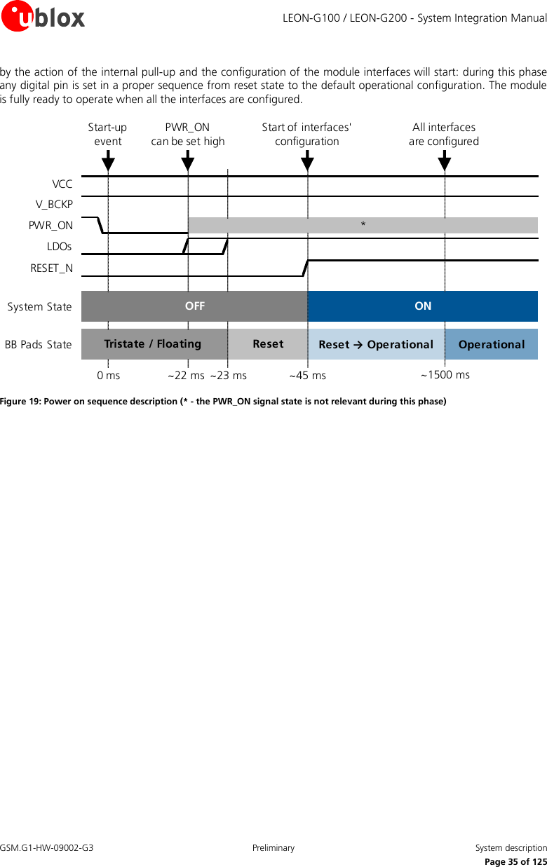
![LEON-G100 / LEON-G200 - System Integration Manual GSM.G1-HW-09002-G3 Preliminary System description Page 34 of 125 Power-on push buttonLEON-G100 / LEON-G20019 PWR_ONLEON-G100 / LEON-G20019 PWR_ONApplication Processor100 k2V_BCKPESD100 k2V_BCKP Figure 18: Power on (PWR_ON) application circuits using a push button or using an application processor 1.6.1.3 RTC alarm The module can be switched-on by the RTC alarm if a valid voltage is applied to VCC pin, when Real Time Clock system reaches a pre-defined scheduled time. The RTC system will then initiate the boot sequence by indicating to the power management unit to turn on power. Also included in this setup is an interrupt signal from the RTC block to indicate to the baseband processor, that a RTC event has occurred. 1.6.1.4 Charger detection on V_CHARGE and CHARGE_SENSE pins (LEON-G200 only) The module can be switched-on by a charger: when a voltage value within the valid range for charger detection is applied to the module V_CHARGE and CHARGE_SENSE pins (See LEON-G100 / LEON-G200 Data Sheet [1]), the module is switched on in charge mode. 1.6.1.5 Additional considerations The module is switched on when the voltage rises up to the VCC normal operating range: the first time that the module is used, it is switched on in this way. Then, the proper way to switch-off the module is by means of the AT+CPWROFF command. When the module is in power-off mode, i.e. the AT+CPWROFF command has been sent and a voltage value within the normal operating range limits is still provided to the VCC pin, the digital input-output pads of the baseband chipset (i.e. all the digital pins of the module) are locked in tri-state (i.e. floating). The power down tri-state function isolates the pins of the module from its environment, when no proper operation of the outputs can be guaranteed. To avoid an increase of the module current consumption in power down mode, any external signal of the digital interfaces connected to the module must be set low or tri-stated when the module is in not-powered mode or in the power-off mode. The module can be switched on from power-off mode by forcing a proper start-up event (i.e. a low level on the PWR_ON pin, or an RTC alarm, or a charger detection). After the detection of a start-up event, all the digital pins of the module are held in tri-state until all the internal LDO voltage regulators are turned on in a defined power-on sequence. Then, as described in Figure 19, the baseband core continues to be held in reset state for a time interval: the module still pulls the RESET_N pin low and any signal from the module digital interfaces is held in reset state. The reset state of all the digital pins is reported in the pin description table of the LEON-G100 / LEON-G200 Data Sheet [1]. When the module releases the RESET_N pin, the level at this pin will be pulled high](https://usermanual.wiki/TransCore/2000B.User-Manual-I/User-Guide-2324779-Page-34.png)
![LEON-G100 / LEON-G200 - System Integration Manual GSM.G1-HW-09002-G3 Preliminary System description Page 36 of 125 1.6.2 Module power off The correct way to switch off LEON-G100 / LEON-G200 modules is by means of the AT command AT+CPWROFF (more details in u-blox AT Commands Manual [2]): in this way the current parameter settings are saved in the module’s non-volatile memory and a proper network detach is performed. An under-voltage shutdown will be done if VCC falls below the extended operating range minimum limit (see LEON-G100 / LEON-G200 Data Sheet [1]), but in this case the current parameter settings are not saved in the module’s non-volatile memory and a proper network detach cannot be performed. When the AT+CPWROFF command is sent, the module starts the switch-off routine replying OK on the AT interface: during this phase, the current parameter settings are saved in the module’s non-volatile memory, a network detach is performed and all module interfaces are disabled (i.e. the digital pins are locked in tri-state by the module). Since the time to perform a network detach depends on the network settings, the duration of this phase can differ from the typical value reported in Figure 20. At the end of the switch-off routine, the module pulls the RESET_N pin low to indicate that it is in power-off mode: all the digital pins are locked in tri-state by the module and all the internal LDO voltage regulators except the RTC supply (V_BCKP) are turned off in a defined power-off sequence. The module remains in power-off mode as long as a switch-on event doesn’t occur (i.e. a low level on the PWR_ON pin, or an RTC alarm, or a charger detection), and enters not-powered mode if the supply is removed from the VCC pin. To avoid an increase of module current consumption in power-down mode, any external signal connected to the module digital pins (UART interface, Digital audio interface, HS_DET, GPIOs) must be tri-stated when the module is in the not-powered or power-off modes. If the external signals connected to the module digital pins cannot be set low or tri-stated, insert a switch (e.g. Texas Instruments SN74CB3Q16244, or Texas Instruments TS5A3159, or Texas Instruments TS5A63157) between the two-circuit connections. Set the switch to high impedance when the module is in power-down mode (to avoid an increase of the module power consumption). Figure 20 describes the power-off sequence. VCCV_BCKPPWR_ON *LDOsRESET_NSystem StateBB Pads State OperationalOFFTristate / Floating ONOperational → Tristate / FloatingAT+CPWROFFsent to the module0 ms~50 ms~400 msOKreplied by the module Figure 20: Power off sequence description (* - the PWR_ON signal state is not relevant during this phase)](https://usermanual.wiki/TransCore/2000B.User-Manual-I/User-Guide-2324779-Page-36.png)
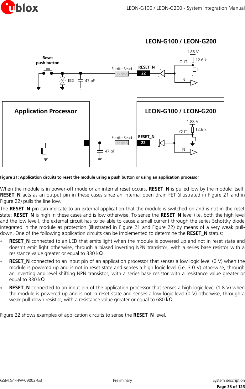
![LEON-G100 / LEON-G200 - System Integration Manual GSM.G1-HW-09002-G3 Preliminary System description Page 37 of 125 1.6.3 Module reset LEON-G100 / LEON-G200 modules can be reset using the RESET_N pin: when the RESET_N pin is forced low for at least 50 ms, an “external” or “hardware” reset is performed, that causes an asynchronous reset of the entire module, except for the RTC. Forcing an “external” or “hardware” reset, the current parameter settings are not saved in the module’s non-volatile memory and a proper network detach is not performed. LEON-G100 / LEON-G200 modules can also be reset by means of the AT command AT+CFUN (more details in u-blox AT Commands Manual [2]): in this case an “internal” or “software” reset is performed, that causes, like the “external” or “hardware” reset, an asynchronous reset of the entire module except for the RTC. Forcing an “internal” or “software” reset, the current parameter settings are saved in the module’s non-volatile memory and a proper network detach is performed. The RESET_N pin is pulled low by the module when the module is in power-off mode or an internal reset occurs. In these cases an internal open drain FET pulls the line low. Name Description Remarks RESET_N Reset signal A series Schottky diode is integrated in the module as protection. An internal 12.6 kΩ pull-up resistor pulls the line to 1.88 V when the module is not in the reset state. An internal open drain FET pulls the line low when an internal reset occurs and when the module is in power down mode. Table 12: Reset pin RESET_N pin ESD sensitivity rating is 1 kV (HBM JESD22-A114F). A higher protection level could be required if the line is externally accessible on the application board. A higher protection level can be achieved mounting an ESD protection (e.g. EPCOS CA05P4S14THSG varistor array) on the line connected to this pin if it is externally accessible on the application board. For more details about the general precautions for ESD immunity about RESET_N pin, refer to chapter 2.5.1. The reset state of each digital pin is reported in the pin description table in the LEON-G100 / LEON-G200 Data Sheet [1]. The electrical characteristics of RESET_N are different from the other digital I/O interfaces. The high and low logic levels have different operating ranges and absolute maximum ratings. The detailed electrical characteristics are described in the LEON-G100 / LEON-G200 Data Sheet [1]. As described in the Figure 21, a series Schottky diode is mounted inside the module on the RESET_N pin to increase the maximum allowed input voltage up to 4.5 V as operating range. Nevertheless the module senses a low level when the RESET_N pin is forced low from the external. As described in Figure 21, the module has an internal pull-up resistor (12.6 kΩ typical) which pulls the level on the RESET_N pin to 1.88 V (typical) when the module is not in reset state. Therefore an external pull-up is not required on the application board. Forcing RESET_N low for at least 50 ms will cause an external reset of the module. When RESET_N is released from the low level, the module automatically starts its power-on reset sequence. If RESET_N is connected to an external device (e.g. an application processor on an application board) an open drain output can be directly connected without any external pull-up. Otherwise, use a push-pull output. Make sure to fix the proper level on RESET_N in all possible scenarios, to avoid unwanted reset of the module. As an ESD immunity test precaution, a 47 pF bypass capacitor (e.g. Murata GRM1555C1H470JA01) and a series ferrite bead (e.g. Murata BLM15HD182SN1) must be added on the RESET_N line pin to avoid a module reset caused by an electrostatic discharge applied to the application board (for more details, refer to chapter 2.5.1).](https://usermanual.wiki/TransCore/2000B.User-Manual-I/User-Guide-2324779-Page-37.png)
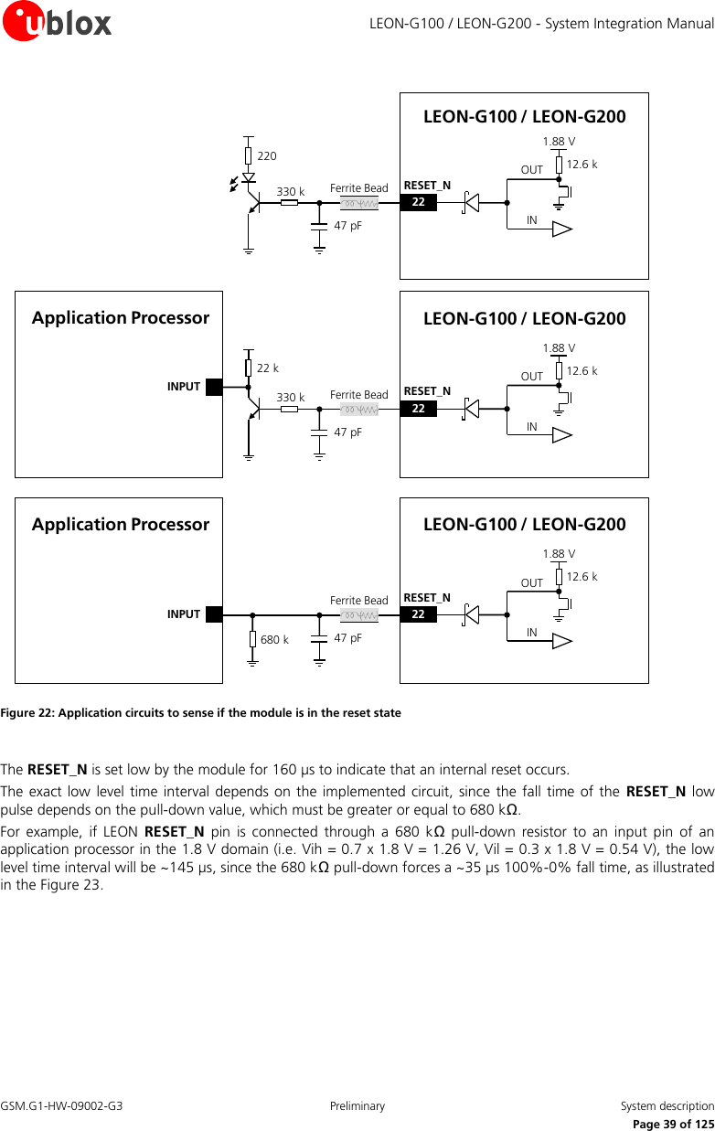
![LEON-G100 / LEON-G200 - System Integration Manual GSM.G1-HW-09002-G3 Preliminary System description Page 40 of 125 Depends on the pull-down strength(~35 µs with 680 k)time [µs]1600LOW = 0 VHIGH = 1.88 VReset state start Reset state endRESET_N Figure 23: RESET_N behavior due to an internal reset 1.6.4 Note: Tri-stated external signal Any external signal connected to the UART interface, I2S interfaces and GPIOs must be tri-stated when the module is in power-down mode, when the external reset is forced low, and during the module power-on sequence (at least for 3 s after the start-up event), to avoid latch-up of circuits and allow a proper boot of the module. If the external signals connected to the wireless module cannot be tri-stated, insert a multi channel digital switch (e.g. Texas Instruments SN74CB3Q16244, TS5A3159, or TS5A63157) between the two-circuit connections and set to high impedance during module power down mode, when external reset is forced low and during power-on sequence. 1.7 RF connection The ANT pin has 50 Ω nominal impedance and must be connected to the antenna through a 50 Ω transmission line to allow transmission and reception of radio frequency (RF) signals in the GSM operating bands. Name Description Remarks ANT RF antenna 50 nominal impedance. Table 13: Antenna pin ANT port ESD immunity rating is 4 kV (according to IEC 61000-4-2). A higher protection level could be required if the line is externally accessible on the application board. A higher protection level can be achieved with an external high pass filter, consists of a 15 pF capacitor (e.g. the Murata GRM1555C1H150JA01) and a 39 nH coil (e.g. Murata LQG15HN39NJ02) connected to the ANT port. The antenna detection functionality will be not provided implementing this high pass filter for ESD protection on the ANT port. Choose an antenna with optimal radiating characteristics for the best electrical performance and overall module functionality. An internal antenna, integrated on the application board, or an external antenna, connected to the application board through a proper 50 Ω connector, can be used. See section 2.4 and 2.2.1.1 for further details regarding antenna guidelines.](https://usermanual.wiki/TransCore/2000B.User-Manual-I/User-Guide-2324779-Page-40.png)
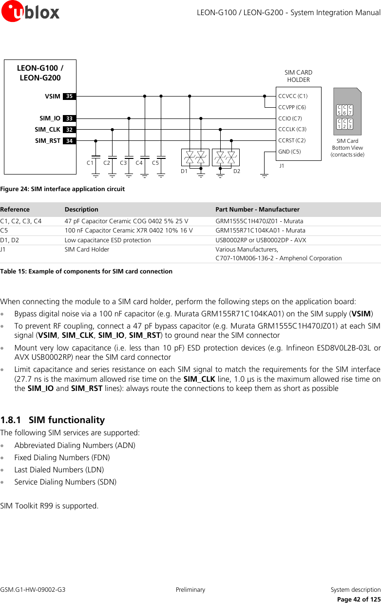
![LEON-G100 / LEON-G200 - System Integration Manual GSM.G1-HW-09002-G3 Preliminary System description Page 41 of 125 The recommendations of the antenna producer for correct installation and deployment (PCB layout and matching circuitry) must be followed. If an external antenna is used, the PCB-to-RF-cable transition must be implemented using either a suitable 50 Ω connector, or an RF-signal solder pad (including GND) that is optimized for 50 Ω characteristic impedance. If antenna supervisor functionality is required, the antenna should have built in DC diagnostic resistor to ground to get proper antenna detection functionality (See section 2.4.3 Antenna detection functionality). 1.8 SIM interface An SIM card interface is provided on the board-to-board pins of the module. High-speed SIM/ME interface is implemented as well as automatic detection of the required SIM supporting voltage. Both 1.8 V and 3 V SIM types are supported: activation and deactivation with automatic voltage switch from 1.8 to 3 V is implemented, according to ISO-IEC 78-16-e specifications. The SIM driver supports the PPS (Protocol and Parameter Selection) procedure for baud-rate selection, according to the values determined by the SIM Card. Table 14 describes the pins related to the SIM interface: Name Description Remarks VSIM SIM supply 1.80 V typical or 2.85 V typical automatically generated by the module SIM_CLK SIM clock 3.25 MHz clock frequency SIM_IO SIM data Internal 4.7 kΩ pull-up to VSIM SIM_RST SIM reset Table 14: SIM Interface pins A low capacitance (i.e. less than 10 pF) ESD protection device (e.g. Infineon ESD8V0L2B-03L or AVX USB0002RP or AVX USB0002DP) must be placed near the SIM card holder on each line (VSIM, SIM_IO, SIM_CLK, SIM_RST). SIM interface pins ESD sensitivity rating is 1 kV (HBM JESD22-A114F): higher protection level is required if the lines are connected to a SIM card holder/connector, so they are externally accessible on the application board. For more details about the general precautions for ESD immunity about SIM pins, refer to chapter 2.5.1. Figure 24 shows the minimal circuit connecting the LEON and the SIM card. This shows the VSIM supply connected to the VPP pin (contact C6) of the SIM card as well as VCC (contact C1). Providing VPP was a requirement for 5 V cards, but under 3GPP TS 51.011 specification [16], 3 V and 1.8 V SIM cards do not require VPP and the mobile equipment (ME) need not provide contact C6. If the ME provides contact C6, then it can either provide the same voltage as on VCC or it can leave the signal open, but it cannot connect VPP to GND.](https://usermanual.wiki/TransCore/2000B.User-Manual-I/User-Guide-2324779-Page-41.png)
![LEON-G100 / LEON-G200 - System Integration Manual GSM.G1-HW-09002-G3 Preliminary System description Page 43 of 125 1.9 Serial Communication 1.9.1 Asynchronous serial interface (UART) The UART interface is a 9-wire unbalanced asynchronous serial interface that provides an AT commands interface, GPRS data and CSD data, software upgrades. The UART interface provides RS-232 functionality conforming with ITU-T V.24 Recommendation [4], with CMOS compatible signal levels: 0 V for low data bit or ON state, and 2.85 V for high data bit or OFF state. An external voltage translator (Maxim MAX3237) is required to provide RS-232 compatible signal levels. For the detailed electrical characteristics refer to the LEON-G100 / LEON-G200 Data Sheet [1]. LEON-G100 / LEON-G200 modules are designed to operate as a GSM/GPRS modem, which represents the data circuit-terminating equipment (DCE) as described by the ITU-T V.24 Recommendation [4]. A customer application processor connected to the module through the UART interface represents the data terminal equipment (DTE). The signal names of the LEON-G100 / LEON-G200 UART interface conform to ITU-T V.24 Recommendation [4]. The UART interface includes the following lines: Name Description Remarks DSR Data set ready Module output, functionality of ITU-T V.24 Circuit 107 (Data set ready) RI Ring Indicator Module output, functionality of ITU-T V.24 Circuit 125 (Calling indicator) DCD Data carrier detect Module output, functionality of ITU-T V.24 Circuit 109 (Data channel received line signal detector) DTR Data terminal ready Module input, functionality of ITU-T V.24 Circuit 108/2 (Data terminal ready) Internal active pull-up to 2.85 V enabled. RTS Ready to send Module hardware flow control input, functionality of ITU-T V.24 Circuit 105 (Request to send) Internal active pull-up to 2.85 V enabled. CTS Clear to send Module hardware flow control output, functionality of ITU-T V.24 Circuit 106 (Ready for sending) TxD Transmitted data Module data input, functionality of ITU-T V.24 Circuit 103 (Transmitted data) Internal active pull-up to 2.85 V enabled. RxD Received data Module data output, functionality of ITU-T V.24 Circuit 104 (Received data) Table 16: UART pins UART interface pins ESD sensitivity rating is 1 kV (HBM JESD22-A114F). A higher protection level could be required if the lines are externally accessible on the application board. A higher protection level can be achieved mounting an ESD protection (e.g. EPCOS CA05P4S14THSG varistor array) on the lines connected to these pins if they are externally accessible on the application board. 1.9.1.1 UART features UART interface is controlled and operated with: AT commands according to 3GPP TS 27.007 [5] AT commands according to 3GPP TS 27.005 [6] AT commands according to 3GPP TS 27.010 [7] u-blox AT commands](https://usermanual.wiki/TransCore/2000B.User-Manual-I/User-Guide-2324779-Page-43.png)
![LEON-G100 / LEON-G200 - System Integration Manual GSM.G1-HW-09002-G3 Preliminary System description Page 44 of 125 All flow control handshakes are supported by the UART interface and can be set by appropriate AT commands (see u-blox AT Commands Manual [2], AT&K command): hardware flow control (RTS/CTS), software flow control (XON/XOFF), or no flow control. Autobauding is supported. It can be enabled or disabled by an AT command (see u-blox AT Commands Manual [2], AT+IPR command). Autobauding is enabled by default. Hardware flow control is enabled by default. For the complete list of supported AT commands and their syntax refer to the u-blox AT Commands Manual [2]. Autobauding result can be unpredictable with spurious data if idle-mode (power-saving) is entered and the hardware flow control is disabled. The following baud rates can be configured using AT commands: 2400 b/s 4800 b/s 9600 b/s 19200 b/s 38400 b/s 57600 b/s 115200 b/s (default value when autobauding is disabled) The following baud-rates are available with autobauding only: 1200 b/s 230400 b/s Automatic frame recognition is supported: this feature is enabled in conjunction with autobauding only, which is enabled by default. The frame format can be: 8N2 (8 data bits, No parity, 2 stop bits) 8E1 (8 data bits, even parity, 1 stop bit) 8O1 (8 data bits, odd parity, 1 stop bit) 8N1 (8 data bits, No parity, 1 stop bit) 7E1 (7 data bits, even parity, 1 stop bit) 7O1 (7 data bits, odd parity, 1 stop bit) The default frame configuration with fixed baud rate is 8N1, described in the Figure 25. D0 D1 D2 D3 D4 D5 D6 D7Start of 1-BytetransferStart Bit(Always 0)Possible Start ofnext transferStop Bit(Always 1)tbit = 1/(Baudrate)Normal Transfer, 8N1 Figure 25: UART default frame format (8N1) description](https://usermanual.wiki/TransCore/2000B.User-Manual-I/User-Guide-2324779-Page-44.png)
![LEON-G100 / LEON-G200 - System Integration Manual GSM.G1-HW-09002-G3 Preliminary System description Page 45 of 125 1.9.1.2 UART signal behavior (AT commands interface case) Refer to Table 2 for a description of operating modes and states referred to in this section. At the module switch-on, before the initialization of the UART interface (each pin is first tristated and then set to its relative reset state reported in the pin description table in LEON-G100 / LEON-G200 Data Sheet [1] (see the power on sequence description in Figure 19). At the end of the boot sequence, the UART interface is initialized, the module is by default in active mode and the UART interface is enabled. The configuration and the behavior of the UART signals after the boot sequence are described below. For a complete description of data and command mode, refer to u-blox AT Commands Manual [2]. RxD signal behavior The module data output line (RxD) is set by default to OFF state (high level) at UART initialization. The module holds RxD in OFF state until no data is transmitted by the module. TxD signal behavior The module data input line (TxD) is set by default to OFF state (high level) at UART initialization. The TxD line is then held by the module in the OFF state if the line is not activated by the DTE: an active pull-up is enabled inside the module on the TxD input. CTS signal behavior The module hardware flow control output (CTS line) is set to the ON state (low level) at UART initialization. If the hardware flow control is enabled (for more details refer to u-blox AT Commands Manual [2], AT&K, AT\Q, AT+IFC commands) the CTS line indicates when the module is in active mode and the UART interface is enabled: the module drives the CTS line to the ON state or to the OFF state when it is either able or not able to accept data from the DTE (refer to chapter 1.9.1.3 for the complete description). If the hardware flow control is not enabled, the CTS line is always held in the ON state after UART initialization. When the power saving configuration is enabled and the hardware flow-control is not implemented in the DTE/DCE connection, data sent by the DTE can be lost: the first character sent when the module is in idle-mode won’t be a valid communication character (refer to chapter 1.9.1.3 for the complete description). During the MUX mode, the CTS line state is mapped to FCon / FCoff MUX command for flow control issues outside the power saving configuration while the physical CTS line is still used as a power state indicator. For more details refer to Mux Implementation Application Note [14]. RTS signal behavior The hardware flow control input (RTS line) is set by default to the OFF state (high level) at UART initialization. The RTS line is then held by the module in the OFF state if the line is not activated by the DTE: an active pull-up is enabled inside the module on the RTS input. If the HW flow control is enabled (for more details refer to u-blox AT Commands Manual [2] AT&K, AT\Q, AT+IFC commands) the RTS line is monitored by the module to detect permission from the DTE to send data to the DTE itself. If the RTS line is set to OFF state, any on-going data transmission from the module is interrupted or any subsequent transmission forbidden until the RTS line changes to ON state. The DTE must be able to still accept a certain number of characters after the RTS line has been set to OFF state: the module guarantees the transmission interruption within 2 characters from RTS state change.](https://usermanual.wiki/TransCore/2000B.User-Manual-I/User-Guide-2324779-Page-45.png)
![LEON-G100 / LEON-G200 - System Integration Manual GSM.G1-HW-09002-G3 Preliminary System description Page 46 of 125 If AT+UPSV=2 is set and HW flow control is disabled, the RTS line is monitored by the module to manage the power saving configuration: When an OFF-to-ON transition occurs on the RTS input line, the module switches from idle-mode to active-mode after 20 ms and the module doesn’t enter idle-mode until the RTS input line is held in the ON state If RTS is set to OFF state by the DTE, the module automatically enters idle-mode whenever possible as in the AT+UPSV=1 configuration (cyclic idle/active mode) For more details refer to chapter 1.9.1.3 and u-blox AT Commands Manual [2], AT+UPSV command. DSR signal behavior If AT&S0 is set, the DSR module output line is set by default to ON state (low level) at UART initialization and is then always held in the ON state. If AT&S1 is set, the DSR module output line is set by default to OFF state (high level) at UART initialization. The DSR line is then set to the OFF state when the module is in command mode and is set to the ON state when the module is in data mode. DTR signal behavior The DTR module input line is set by default to OFF state (high level) at UART initialization. The DTR line is then held by the module in the OFF state if the line is not activated by the DTE: an active pull-up is enabled inside the module on the DTR input. Module behavior according to DTR status depends on the AT command configuration (see u-blox AT Commands Manual [2], AT&D command). DCD signal behavior If AT&C0 is set, the DCD module output line is set by default to ON state (low level) at UART initialization and is then always held in the ON state. If AT&C1 is set, the DCD module output line is set by default to OFF state (high level) at UART initialization. The DCD line is then set by the module in accordance with the carrier detect status: ON if the carrier is detected, OFF otherwise. In case of voice call DCD is set to ON state when the call is established. For a data call there are the following scenarios: GPRS data communication: Before activating the PPP protocol (data mode) a dial-up application must provide the ATD*99***<context_number># to the module: with this command the module switches from command mode to data mode and can accept PPP packets. The module sets the DCD line to the ON state, then answers with a CONNECT to confirm the ATD*99 command. The DCD ON is not related to the context activation but with the data mode CSD data call: To establish a data call the DTE can send the ATD<number> command to the module which sets an outgoing data call to a remote modem (or another data module). Data can be transparent (non reliable) or non transparent (with the reliable RLP protocol). When the remote DCE accepts the data call, the module DCD line is set to ON and the CONNECT <communication baudrate> string is returned by the module. At this stage the DTE can send characters through the serial line to the data module which sends them through the network to the remote DCE attached to a remote DTE RI signal behavior The RI module output line is set by default to the OFF state (high level) at UART initialization. Then, during an incoming call, the RI line is switched from OFF state to ON state with a 4:1 duty cycle and a 5 s period (ON for 1 s, OFF for 4 s, see Figure 26), until the DTE attached to the module sends the ATA string and the module accepts the incoming data call. The RING string sent by the module (DCE) to the serial port at constant time intervals is not correlated with the switch of the RI line to the ON state.](https://usermanual.wiki/TransCore/2000B.User-Manual-I/User-Guide-2324779-Page-46.png)
![LEON-G100 / LEON-G200 - System Integration Manual GSM.G1-HW-09002-G3 Preliminary System description Page 47 of 125 Figure 26: RI behavior during an incoming call The RI line can notify an SMS arrival. When the SMS arrives, the RI line switches from OFF to ON for 1 s (see Figure 27), if the feature is enabled by the proper AT command (refer to u-blox AT Commands Manual [2], AT+CNMI command). Figure 27: RI behavior at SMS arrival This behavior allows the DTE to remain in power saving mode until the DCE related event requests service. If more than one SMS arrives coincidently or in quick succession the RI line will be independently triggered, although the line will not be deactivated between each event. As a result, the RI line may remain in the ON state for more than 1 second. If an incoming call is answered within less than 1 second (with ATA or if auto-answering is set to ATS0=1) then the RI line will be set to OFF earlier. As a result: RI line monitoring can’t be used by the DTE to determine the number of received SMSes In case of multiple events (incoming call plus SMS received), the RI line can’t be used to discriminate between the two events, but the DTE must rely on the subsequent URCs and interrogate the DCE with the proper commands 1.9.1.3 UART and power-saving The power saving configuration is controlled by the AT+UPSV command (for the complete description refer to u-blox AT Commands Manual [2], AT+UPSV command). When power saving is enabled, the module automatically enters idle-mode whenever possible, otherwise the active-mode is maintained by the module. The AT+UPSV command sets the module power saving configuration, but also configures the UART behavior in relation to the power saving configuration. The conditions for the module entering idle-mode also depend on the UART power saving configuration. The different power saving configurations that can be set by the AT+UPSV command are described in the following subchapters and are summarized in Table 17. For more details on the command description, refer to u-blox AT commands Manual [2]. SMS arrives time [s] 0 RI ON RI OFF 1s SMS time [s] 0 RI ON RI OFF 1s 1stime [s]151050RI ONRI OFFCall incomes1stime [s]151050RI ONRI OFFCall incomes](https://usermanual.wiki/TransCore/2000B.User-Manual-I/User-Guide-2324779-Page-47.png)
![LEON-G100 / LEON-G200 - System Integration Manual GSM.G1-HW-09002-G3 Preliminary System description Page 49 of 125 Every subsequent character received during the active-mode, resets and restarts the timer; hence the active-mode duration can be extended indefinitely. The behavior of hardware flow-control output (CTS line) during normal module operations with power-saving and HW flow control enabled (cyclic idle-mode and active-mode) is illustrated in Figure 28. Figure 28: CTS behavior with power saving enabled: the CTS line indicates when the module is able (CTS = ON = low level) or not able (CTS = OFF = high level) to accept data from the DTE and communicate through the UART interface AT+UPSV=2: power saving enabled and controlled by the RTS line The module behavior is the same as for AT+UPSV=1 case if the RTS line is set to OFF by the DTE. When an OFF-to-ON transition occurs on the RTS input line, the module switches from idle-mode to active-mode after 20 ms and then the module doesn’t enter the idle-mode until the RTS input line is held in the ON state. This configuration can only be enabled with the module HW flow control disabled. Even if HW flow control is disabled, if the RTS line is set to OFF by the DTE, the CTS line is set by the module accordingly to its power saving configuration (like for AT+UPSV=1 with HW flow control enabled). When the RTS line is set to OFF by the DTE, the timeout to enter idle-mode from the last data received at the serial port during the active-mode is the one previously set with the AT+UPSV=1 configuration or it is the default value. time [s] CTS ON CTS OFF max ~2.1 s UART disabled min ~11 ms UART enabled ~9.2 s (default) UART enabled Data input time [s] CTS ON CTS OFF max ~2.1 s UART disabled min ~11 ms UART enabled ~9.2 s (default) UART enabled](https://usermanual.wiki/TransCore/2000B.User-Manual-I/User-Guide-2324779-Page-49.png)
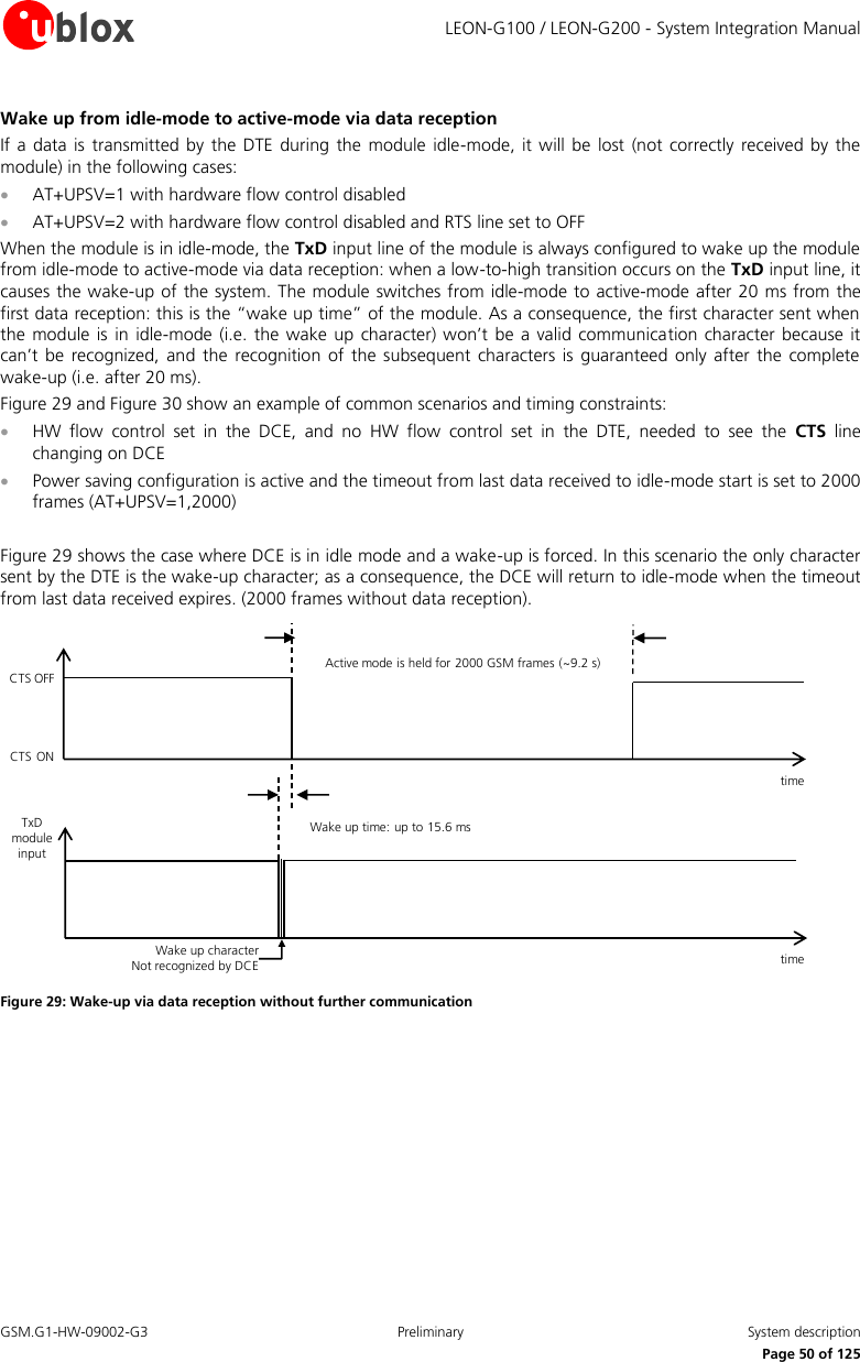
![LEON-G100 / LEON-G200 - System Integration Manual GSM.G1-HW-09002-G3 Preliminary System description Page 51 of 125 Figure 30 shows the case where in addition to the wake-up character further (valid) characters are sent. The wake up character wakes-up the DCE. The other characters must be sent after the “wake up time” of 20 ms. If this condition is met, the characters are recognized by the DCE. The DCE is allowed to re-enter idle-mode after 2000 GSM frames from the latest data reception. CTS OFFCTS ONActive mode is held for 2000 GSM frames (~9.2s) after the last data receivedtime Wake up time: up to 15.6 mstime TxD module inputWake up character Not recognized by DCEValid characters Recognized by DCE Figure 30: Wake-up via data reception with further communication The “wake-up via data reception” feature can’t be disabled. The “wake-up via data reception” feature can be used in both AT+UPSV=1 and AT+UPSV=2 case (when RTS line is set to OFF). In command mode, if autobauding is enabled and HW flow control is not implemented by the DTE, the DTE must always send a character to the module before the “AT” prefix set at the beginning of each command line: the first character will be ignored if the module is in active-mode, or it will represent the wake up character if the module is in idle-mode. In command mode, if autobauding is disabled, the DTE must always send a dummy “AT” to the module before each command line: the first character will not be ignored if the module is in active-mode (i.e. the module will reply “OK”), or it will represent the wake up character if the module is in idle-mode (i.e. the module won’t reply). No wake-up character or dummy “AT” is required from the DTE during connected-mode since the module continues to be in active-mode and doesn’t need to be woken-up. Furthermore in data mode a wake-up character or a dummy “AT” would affect the data communication. 1.9.1.4 UART application circuits Providing the full RS-232 functionality (using the complete V.24 link) For complete RS-232 functionality conforming to ITU-T Recommendation [4] in DTE/DCE serial communication, the complete UART interface of the module (DCE) must be connected to the DTE as described in Figure 31.](https://usermanual.wiki/TransCore/2000B.User-Manual-I/User-Guide-2324779-Page-51.png)
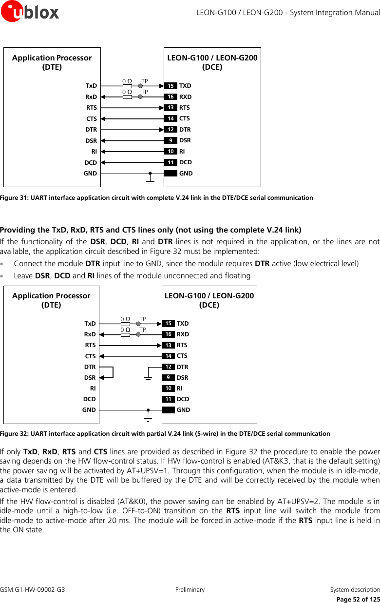
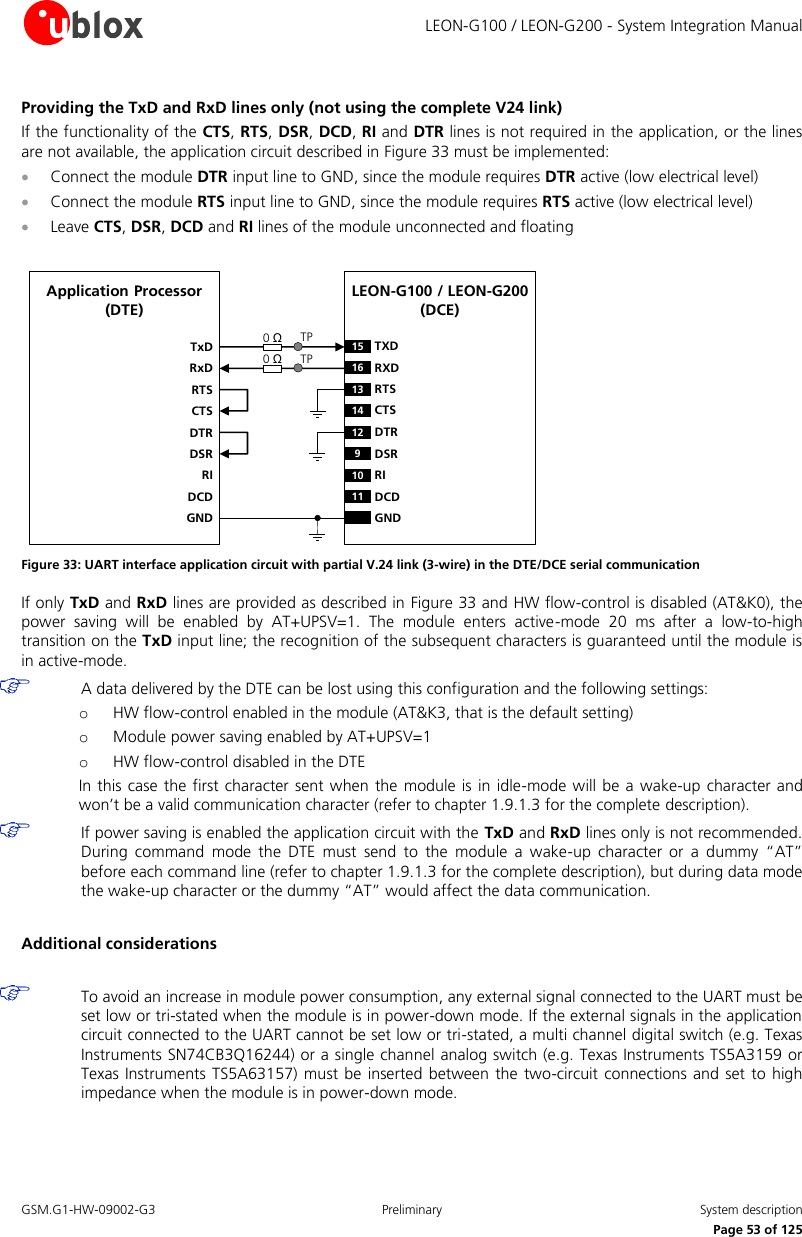
![LEON-G100 / LEON-G200 - System Integration Manual GSM.G1-HW-09002-G3 Preliminary System description Page 54 of 125 It is highly recommended to provide on an application board a direct access to RxD and TxD lines of the module (in addition to access to these lines from an application processor). This enables a direct connection of PC (or similar) to the module for execution of Firmware upgrade over the UART. The module FW upgrade over UART (using the RxD and TxD pins) starts at the module switch-on or when the module is released from the reset state: it is suggested to provide access to the PWR_ON pin, or to provide access to the RESET_N pin, or to provide access to the enabling of the DC supply connected to the VCC pin, to start the module firmware upgrade over the UART. 1.9.1.5 MUX Protocol (3GPP 27.010) The module has a software layer with MUX functionality complaint with 3GPP 27.010 [7]. This is a data link protocol (layer 2 of OSI model) using HDLC-like framing and operates between the module (DCE) and the application processor (DTE). The protocol allows simultaneous sessions over the UART. Each session consists of a stream of bytes transferring various kinds of data like SMS, CBS, GPRS, AT commands in general. This permits, for example, SMS to be transferred to the DTE when a data connection is in progress. The following channels are defined: Channel 0: control channel Channel 1 – 5: AT commands /data connection Channel 6: GPS tunneling For more details refer to GSM Mux implementation Application Note [14].](https://usermanual.wiki/TransCore/2000B.User-Manual-I/User-Guide-2324779-Page-54.png)
![LEON-G100 / LEON-G200 - System Integration Manual GSM.G1-HW-09002-G3 Preliminary System description Page 55 of 125 1.9.2 DDC (I2C) interface 1.9.2.1 Overview An I2C compatible Display Data Channel (DDC) interface for communication with u-blox GPS receivers is available on LEON-G100 / LEON-G200 modules. This interface is intended exclusively to access u-blox GPS receivers. Name Description Remarks SCL I2C bus clock line Fixed open drain. External pull-up required. SDA I2C bus data line Fixed open drain. External pull-up required. Table 18: DDC (I2C) pins DDC (I2C) interface pins ESD sensitivity rating is 1 kV (HBM JESD22-A114F). A higher protection level could be required if the lines are externally accessible on the application board. A higher protection level can be achieved mounting an ESD protection (e.g. EPCOS CA05P4S14THSG varistor array) on the lines connected to these pins if they are externally accessible on the application board. u-blox has implemented special features in LEON-G100 / LEON-G200 modules to ease the design effort required to integrate a u-blox wireless module with a u blox GPS receiver. Combining a LEON-G100 / LEON-G200 wireless module with a u-blox GPS receiver allows designers full access to the GPS receiver directly via the wireless module: it relays control messages to the GPS receiver via a dedicated DDC (I2C) interface. A 2nd interface connected to the GPS receiver isn’t necessary: AT commands via the UART serial interface of the wireless module allow full control of the GPS receiver from any host processor. LEON-G100 / LEON-G200 modules feature embedded u-blox GPS aiding functionalities for enhanced GPS performance. These provide decreased Time To First Fix (TTFF) and allow faster position calculation with higher accuracy. For more details regarding the handling of the DDC (I2C) interface and the GPS aiding features refer to u-blox AT Commands Manual [2] (AT+UGPS, AT+UGPRF, AT+UGPIOC commands) and GPS Implementation Application Note [3].](https://usermanual.wiki/TransCore/2000B.User-Manual-I/User-Guide-2324779-Page-55.png)
![LEON-G100 / LEON-G200 - System Integration Manual GSM.G1-HW-09002-G3 Preliminary System description Page 56 of 125 1.9.2.2 DDC application circuit General considerations The DDC (I2C) interface of the LEON-G100 / LEON-G200 modules is used only to connect the wireless module to a u-blox GPS receiver: the DDC (I2C) interface is enabled by the AT+UGPS command only (for more details refer to u-blox AT Commands Manual [2]). The SDA and SCL lines must be connected to the DDC (I2C) interface pins of the u-blox GPS receiver (i.e. the SDA2 and SCL2 pins of the u-blox GPS receiver) on the application board. To be complaint with the I2C bus specifications, the module pads of the bus interface are open drain output and pull-up resistors must be used. Since the pull-up resistors are not mounted on the module, they must be mounted externally. Resistor values must conform to the I2C bus specifications [8]. If LEON-G100 / LEON-G200 modules are connected through the DDC bus to a u-blox GPS receiver (only one device can be connected on the DDC bus), use a pull-up resistor of 4.7 k. Pull-up resistors must be connected to a supply voltage of 2.85 V (typical), since this is the voltage domain of the DDC pins (for detailed electrical characteristics see the LEON-G100 / LEON-G200 Data Sheet [1]). DDC Slave-mode operation is not supported, the module can act as master only. Two lines, serial data (SDA) and serial clock (SCL), carry information on the bus. SCL is used to synchronize data transfers, and SDA is the data line. Since both lines are open drain outputs, the DDC devices can only drive them low or leave them open. The pull-up resistor pulls the line up to the supply rail if no DDC device is pulling it down to GND. If the pull-ups are missing, SCL and SDA lines are undefined and the DDC bus will not work. The signal shape is defined by the values of the pull-up resistors and the bus capacitance. Long wires on the bus will increase the capacitance. If the bus capacitance is increased, use pull-up resistors with nominal resistance value lower than 4.7 k, to match the I2C bus specifications [8] regarding rise and fall times of the signals. Capacitance and series resistance must be limited on the bus to match the I2C specifications [8] (1.0 µs is the maximum allowed rise time on the SCL and SDA lines): route connections as short as possible. If the pins are not used as DDC bus interface, they can be left floating on the application board. LEON-G100-06x / LEON-G200-06S and subsequent versions LEON-G100-06x / LEON-G200-06S and subsequent versions support these GPS aiding types: Local aiding AssistNow Online AssistNow Offline AssistNow Autonomous The embedded GPS aiding features can be used only if the DDC (I2C) interface of the wireless module is connected to the u-blox GPS receivers. The GPIO pins can handle: The power on/off of the GPS receiver (“GPS supply enable” function provided by GPIO2) The wake up from idle-mode when the GPS receiver is ready to send data (“GPS data ready” function provided by GPIO3) The RTC synchronization signal to the GPS receiver (“GPS RTC sharing” function provided by GPIO4) GPIO2 is by default configured to provide the “GPS supply enable” function (parameter <gpio_mode> of AT+UGPIOC command set to 3 by default), to enable or disable the supply of the u-blox GPS receiver connected to the wireless module by the AT+UGPS command. The pin is set as Output / High, to switch on the u-blox GPS receiver, if the parameter <mode> of AT+UGPS command is set to 1 Output / Low, to switch off the u-blox GPS receiver, if the parameter <mode> of AT+UGPS command is set to 0 (default setting)](https://usermanual.wiki/TransCore/2000B.User-Manual-I/User-Guide-2324779-Page-56.png)
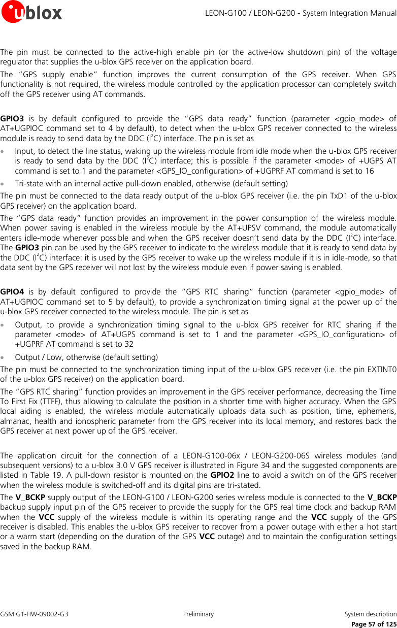
![LEON-G100 / LEON-G200 - System Integration Manual GSM.G1-HW-09002-G3 Preliminary System description Page 59 of 125 The pin must be connected to the active-high enable pin (or the active-low shutdown pin) of the voltage regulator that supplies the u-blox GPS receiver on the application board. The “GPS supply enable” function improves the power consumption of the GPS receiver. When GPS functionality is not required, the wireless module controlled by the application processor can completely switch off the GPS receiver using AT commands. The application circuit for connecting LEON-Gx00-04S and LEON-Gx00-05S versions to a u-blox 3.0 V GPS receiver is illustrated in Figure 35, and the suggested components are listed in Table 20. A pull-down resistor is mounted on the GPIO2 line to avoid a switch-on of the GPS receiver when the wireless module is switched-off and its digital pins are tri-stated. The V_BCKP supply output of the LEON-G100 / LEON-G200 series wireless module is connected to the V_BCKP backup supply input pin of the GPS receiver to provide the supply for the GPS real time clock and backup RAM when the VCC supply of the wireless module is within its operating range and the VCC supply of the GPS receiver is disabled. This enables the u-blox GPS receiver to recover from a power outage with either a hot start or a warm start (depending on the duration of the GPS VCC outage) and to maintain the configuration settings saved in the backup RAM. LEON-Gx00-04S LEON-Gx00-05SR1INOUTGNDGPS LDORegulatorSHDNu-blox3.0 V GPS receiverSDA2SCL2R23V0 3V0VMAIN3V0U121 GPIO2SDASCLC13130VCCR32V_BCKPV_BCKP Figure 35: Application circuit for LEON-Gx00-04S and LEON-Gx00-05S versions and u-blox 3.0 V GPS receivers Reference Description Part Number - Manufacturer R1, R2 4.7 kΩ Resistor 0402 5% 0.1 W RC0402JR-074K7L - Yageo Phycomp R3 47 kΩ Resistor 0402 5% 0.1 W RC0402JR-0747KL - Yageo Phycomp U1 Voltage Regulator for GPS Receiver See GPS Receiver Hardware Integration Manual Table 20: Component for application circuit for LEON-Gx00-04S and LEON-Gx00-05S versions and u-blox 3.0 V GPS receivers Comment [tgri1]: This paragraph is repeated in the previous description (LEON-Gx00-06 and subsequent versions). Would it be possible to restructure or add a cross reference to prevent the repetition?](https://usermanual.wiki/TransCore/2000B.User-Manual-I/User-Guide-2324779-Page-59.png)
![LEON-G100 / LEON-G200 - System Integration Manual GSM.G1-HW-09002-G3 Preliminary System description Page 60 of 125 1.10 Audio LEON-G100 / LEON-G200 modules provide four analog and one digital audio interfaces: Two microphone inputs: First microphone input can be used for direct connection of the electret condenser microphone of a handset. This input is used when the main uplink audio path is “Handset Microphone” (refer to u-blox AT Commands Manual [2]; AT+USPM command: <main_uplink> parameter) Second microphone input can be used for direct connection of the electret condenser microphone of a headset. This input is used when the main uplink audio path is “Headset Microphone” (refer to u-blox AT Commands Manual [2]; AT+USPM command: <main_uplink> parameter) Two speaker outputs: First speaker output is a single ended low power audio output that can be used to directly connect the receiver (earpiece) of a handset or a headset. This output is used when the main downlink audio path is “Normal earpiece” or “Mono headset” (refer to u-blox AT Commands Manual [2]; AT+USPM command: <main_downlink> parameter). These two downlink path profiles use the same physical output but have different sets of audio parameters (Refer to u-blox AT Commands Manual [2]: AT+USGC, AT+UDBF, AT+USTN commands) Second speaker output is a differential high power audio output that can be used to directly connect a speaker or a loud speaker used for ring-tones or for speech in hands-free mode. This output is used when audio downlink path is “Loudspeaker” (refer to u-blox AT Commands Manual [2]; AT+USPM command, <main_downlink> and <alert_sound> parameters) Headset detection input: If enabled, causes the automatic switch of uplink audio path to “Headset Microphone” and downlink audio path to “Mono headset”. Enabling/disabling the detection can be controlled by parameter <headset_indication> in AT+USPM command (refer to u-blox AT Commands Manual [2]) I2S digital audio interface: This path is selected when parameters <main_uplink> and <main_downlink> in AT+USPM command (refer to u-blox AT Commands Manual [2]) are respectively “I2S input line” and “I2S output line” Not all combinations of Input-Output audio paths are allowed. Check audio command AT+USPM in u-blox AT Commands Manual [2] for allowed combinations of audio path and for their switching during different use cases (speech/alert tones). The default values for audio parameters tuning commands (Refer to u-blox AT Commands Manual [2]; AT+UMGC, AT+UUBF, AT+UHFP, AT+USGC, AT+UDBF, AT+USTN commands) are tuned for audio device connected as suggested above (i.e. Handset microphone connected on first microphone input, headset microphone on second microphone input). For a different connection, (i.e. connection of a Hands Free microphone) these parameters should be changed on the audio path corresponding to the connection chosen. 1.10.1 Analog Audio interface 1.10.1.1 Uplink path (microphone inputs) The TX (uplink) path of the analog audio front-end on the module consists of two identical microphone circuits. Two electret condenser microphones can be directly connected to the two available microphone inputs. The main required electrical specifications for the electret condenser microphone are 2.2 k as maximum output impedance at 1 kHz and 2 V maximum standard operating voltage. LEON-G100 / LEON-G200 pins related to the uplink path (microphones inputs) are: First microphone input:](https://usermanual.wiki/TransCore/2000B.User-Manual-I/User-Guide-2324779-Page-60.png)
![LEON-G100 / LEON-G200 - System Integration Manual GSM.G1-HW-09002-G3 Preliminary System description Page 61 of 125 MIC_BIAS1: single ended supply to the first microphone and represents the microphone signal input MIC_GND1: local ground for the first microphone Second microphone input: MIC_BIAS2: single ended supply to the second microphone and represents the microphone signal input MIC_GND2: local ground for the second microphone For a description of the internal function blocks see Figure 41. 1.10.1.2 Downlink path (speaker outputs) The RX (downlink) path of the analog audio front-end of the module consists of two speaker outputs available on the following pins: First speaker output: HS_P: low power single ended audio output. This pin is internally connected to the output of the single ended audio amplifier of the chipset Second speaker output: SPK_N/SPK_P: high power differential audio output. These two pins are internally connected to the output of the high power differential audio amplifier of the chipset See Figure 41 for a description of the internal function blocks. Warning: excessive sound pressure from headphones can cause hearing loss. Detailed electrical characteristics of the low power single-ended audio receive path and the high power differential audio receive path can be found in LEON-G100 / LEON-G200 Data Sheet [1]. Table 21 lists the signals related to analog audio functions. Name Description Remarks HS_DET Headset detection input Internal active pull-up to 2.85 V enabled. HS_P First speaker output with low power single-ended analog audio This audio output is used when audio downlink path is “Normal earpiece“ or “Mono headset“ SPK_P Second speaker output with high power differential analog audio This audio output is used when audio downlink path is “Loudspeaker“. SPK_N Second speaker output with power differential analog audio output This audio output is used when audio downlink path is “Loudspeaker“. MIC_BIAS2 Second microphone analog signal input and bias output This audio input is used when audio uplink path is set as “Headset Microphone“. Single ended supply output and signal input for the second microphone. MIC_GND2 Second microphone analog reference Local ground of second microphone. Used for “Headset microphone” path. MIC_GND1 First microphone analog reference Local ground of the first microphone. Used for “Handset microphone” path MIC_BIAS1 First microphone analog signal input and bias output This audio input is used when audio uplink path is set as “Handset Microphone“. Single ended supply output and signal input for first microphone. Table 21: Analog Audio Signal Pins All audio lines on an Application Board must be routed in pairs, be embedded in GND (have the ground lines as close as possible to the audio lines), and maintain distance from noisy lines such as VCC and from components such as switching regulators. Audio pins ESD sensitivity rating is 1 kV (HBM JESD22-A114F). A higher protection level could be required if the lines are externally accessible on the application board. A higher protection level can be achieved mounting an ESD protection (e.g. EPCOS CA05P4S14THSG varistor array) on the lines connected to these pins if they are externally accessible on the application board. If the audio pins are not used, they can be left floating on the application board.](https://usermanual.wiki/TransCore/2000B.User-Manual-I/User-Guide-2324779-Page-61.png)
![LEON-G100 / LEON-G200 - System Integration Manual GSM.G1-HW-09002-G3 Preliminary System description Page 62 of 125 1.10.1.3 Handset mode Handset mode is the default audio operating mode of LEON-G100 / LEON-G200 modules. In this mode the main uplink audio path is “Handset microphone”, the main downlink audio path is “Normal earpiece” (refer to u-blox AT Commands Manual [2]; AT+USPM command: <main_uplink>, <main_downlink> parameters). Handset microphone must be connected to inputs MIC_BIAS1/MIC_GND1 Handset receiver must be connected to output HS_P Figure 36 shows an example of an application circuit connecting a handset (with a 2.2 kΩ electret microphone and a 32 Ω receiver) to the LEON-G100 / LEON-G200 modules. The following actions should be done on the application circuit: Mount a series capacitor on the HS_P line to decouple the bias Mount a 10 µF ceramic capacitor (e.g. Murata GRM188R60J106M) if connecting a 32 Ω receiver, or a load with greater impedance (such as a single ended analog input of a codec). Otherwise if a 16 Ω receiver is connected to the line, a ceramic capacitor with greater nominal capacitance must be used: a 22 µF series capacitor (e.g. Murata GRM21BR60J226M) is required Mount a 82 nH series inductor (e.g. Murata LQG15HS82NJ02) on each microphone line and a 27 pF bypass capacitor (e.g. Murata GRM1555C1H270J) on all audio lines to minimize RF coupling and TDMA noise LEON-G100 / LEON-G200C1AUDIO HANDSET CONNECTORC2 C3J14321L1L237HS_P43MIC_GND144MIC_BIAS1C4D1 Figure 36: Handset connector application circuit Reference Description Part Number - Manufacturer C1, C2, C3 27 pF Capacitor Ceramic COG 0402 5% 25 V GRM1555C1H270JZ01 - Murata C4 10 µF Capacitor Ceramic X5R 0603 20% 6.3V GRM188R60J106M - Murata L1, L2 82 nH Multilayer inductor 0402 (self resonance frequency ~1 GHz) LQG15HS82NJ02 - Murata J1 Audio Handset Jack Connector, 4Ckt (4P4C) 52018-4416 - Molex D1 Varistor Array for ESD protection CA05P4S14THSG - EPCOS Table 22: Example of components for handset connection 1.10.1.4 Headset mode The audio path is automatically switched from handset mode to headset mode when a rising edge is detected by the module on HS_DET pin. The audio path returns to the handset mode when the line returns to low level. In headset mode the main uplink audio path is “Headset microphone”, the main downlink audio path is “Mono headset” (refer to u-blox AT Commands Manual [2]; AT+USPM command: <main_uplink>, <main_downlink> parameters). The audio path used in headset mode: Headset microphone must be connected to MIC_BIAS2/MIC_GND2 Headset receiver must be connected to HS_P](https://usermanual.wiki/TransCore/2000B.User-Manual-I/User-Guide-2324779-Page-62.png)
![LEON-G100 / LEON-G200 - System Integration Manual GSM.G1-HW-09002-G3 Preliminary System description Page 63 of 125 Figure 37 shows an application circuit connecting a headset (with a 2.2 kΩ electret microphone and a 32 Ω receiver) to the LEON-G100 / LEON-G200 modules. Pin 2 & 5 are shorted in the headset connector, causing HS_DET to be pulled low. When the headset plug is inserted HS_DET is pulled up internally by the module, causing a rising edge for detection. Perform the following steps on the application board (as shown in Figure 37; the list of components to be mounted is shown in Table 23): Mount a series capacitor on the HS_P line to decouple the bias. 10 µF ceramic capacitor (e.g. Murata GRM188R60J106M) is required if a 32 Ω receiver or a load with greater impedance (as a single ended analog input of a codec) is connected to the line. 22 µF series capacitor (e.g. Murata GRM21BR60J226M) is required if a 16 Ω receiver is connected to the line Mount a 82 nH series inductor (e.g. Murata LQG15HS82NJ02) on each microphone line, and a 27 pF bypass capacitor (e.g. Murata GRM1555C1H270J) on all audio lines to minimize RF coupling and the TDMA noise LEON-G100 / LEON-G200C4AUDIO HEADSET CONNECTORC1 C2 C3J1253461L1L218HS_DET37HS_P42MIC_GND241MIC_BIAS2D1 Figure 37: Headset mode application circuit Reference Description Part Number - Manufacturer C1, C2, C3 27 pF Capacitor Ceramic COG 0402 5% 25 V GRM1555C1H270JZ01 - Murata C4 10 µF Capacitor Ceramic X5R 0603 20% 6.3V GRM188R60J106M - Murata L1, L2 82nH Multilayer inductor 0402 (self resonance frequency ~1 GHz) LQG15HS82NJ02 - Murata J1 Audio Headset 2.5 mm Jack Connector SJ1-42535TS-SMT - CUI, Inc. D1 Varistor Array for ESD protection CA05P4S14THSG - EPCOS Table 23: Example of components for headset jack connection 1.10.1.5 Hands-free mode Hands-free mode can be implemented using a loudspeaker and a dedicated microphone. Hands-free functionality is implemented using appropriate DSP algorithms for voice-band handling (echo canceller and automatic gain control), managed via software (Refer to u-blox AT Commands Manual [2]; AT+UHFP command). In this mode the main downlink audio path must be “Loudspeaker”, the main uplink audio path can be “Handset microphone” or “Headset microphone” (refer to u-blox AT Commands Manual [2]; AT+USPM command: <main_uplink>, <main_downlink> parameters). Use of an uplink audio path for hands-free makes it unavailable for another device (handset/headset). Therefore: Microphone can be connected to the input pins MIC_BIAS1/MIC_GND1 or MIC_BIAS2/MIC_GND2 High power loudspeaker must be connected to the output pins SPK_P/SPK_N](https://usermanual.wiki/TransCore/2000B.User-Manual-I/User-Guide-2324779-Page-63.png)
![LEON-G100 / LEON-G200 - System Integration Manual GSM.G1-HW-09002-G3 Preliminary System description Page 64 of 125 The default parameters for audio uplink profiles “Handset microphone” and “Headset microphone” (refer to u-blox AT Commands Manual [2]; AT+UMGC, AT+UUBF, AT+UHFP) are for a handset and a headset microphone. To implement hands-free mode, these parameters should be changed on the audio path corresponding to the connection chosen. Procedure to tune parameters for hands-free mode (gains, echo canceller) can be found in LEON Audio Application Note [12]. When hands-free mode is enabled, the audio output signal on HS_P is disabled. The physical width of the high-power audio outputs lines on the application board must be wide enough to minimize series resistance. Figure 38 shows an application circuit for hands-free mode. In this example the LEON-G100 / LEON-G200 modules are connected to an 8 Ω speaker and a 2.2 kΩ electret microphone. Insert an 82 nH series inductor (e.g. Murata LQG15HS82NJ02) on each microphone line, and a 27 pF bypass capacitor (e.g. Murata GRM1555C1H270J) on all audio lines to minimize RF coupling and the TDMA noise. LEON-G100 / LEON-G200SPKC1 C2L2L1MICC3 C439SPK_N38SPK_P43MIC_GND144MIC_BIAS1 Figure 38: Hands free mode application circuit Reference Description Part Number - Manufacturer C1, C2, C3, C4 27 pF Capacitor Ceramic COG 0402 5% 25 V GRM1555C1H270JZ01 - Murata L1, L2 82nH Multilayer inductor 0402 (self resonance frequency ~1 GHz) LQG15HS82NJ02 - Murata SPK Loudspeaker MIC Active Elected Microphone Table 24: Example of components for hands-free connection 1.10.1.6 Connection to an external analog audio device MIC_BIAS1 / MIC_GND single ended analog audio inputs and the HS_P single ended analog audio output of LEON-G100 / LEON-G200 can be used to connect the module to an external analog audio device. If the external analog audio device is provided with a single ended analog audio input, the HS_P single ended output of the module must be connected to the single ended input of the external audio device by a DC-block 10 µF series capacitor (e.g. Murata GRM188R60J106M) to decouple the bias present at the module output (see HS_P common mode output voltage in LEON-G100 / LEON-G200 Data Sheet [1]). Use a suitable power-on sequence to avoid audio bump due to charging of the capacitor: the final audio stage should always be the last one enabled. If the external analog audio device is provided with a differential analog audio input, a proper single ended to differential circuit must be inserted from the HS_P single ended output of the module to the differential input of the external audio device. A simple application circuit is described in Figure 39: a DC-block 10 µF series capacitor](https://usermanual.wiki/TransCore/2000B.User-Manual-I/User-Guide-2324779-Page-64.png)
![LEON-G100 / LEON-G200 - System Integration Manual GSM.G1-HW-09002-G3 Preliminary System description Page 65 of 125 (e.g. Murata GRM188R60J106M) is provided to decouple the bias present at the module output. A voltage divider is provided to correctly adapt the signal level from the module output to the external audio device input. The DC-block series capacitor acts as high-pass filter for audio signals, with cut-off frequency depending on both the values of capacitor and on the input impedance of the audio device. For example: in case of a single ended connection to 600 external device, the 10 µF capacitor will set the -3 dB cut-off frequency to 103 Hz. The high-pass filter has a low enough cut-off to not impact the audio signal frequency response. If the external analog audio device is provided with a single ended analog audio output, the MIC_BIAS1 single ended input of the module must be connected to the single ended output of the external audio device by a DC-block 10 µF series capacitor (e.g. Murata GRM188R60J106M) to decouple the bias present at the module input (see MIC_BIAS1 microphone supply characteristics in LEON-G100 / LEON-G200 Data Sheet [1]). If the external analog audio device is provided with a differential analog audio output, a proper differential to single ended circuit must be inserted from the differential output of the external audio device to the MIC_BIAS1 single ended input of the module. Figure 39 describes a simple application circuit: a DC-block 10 µF series capacitor (e.g. Murata GRM188R60J106M) is provided to decouple the bias present at the module input, and a voltage divider is provided to correctly adapt the signal level from the external audio device output to the module input. Use a suitable power-on sequence to avoid audio bump due to capacitor charging: the final audio stage should always be the last one enabled. Additional circuitry should be inserted depending on the external audio device characteristics. To enable the audio path corresponding to these input/output, refer to u-blox AT Commands Manual [2], AT+USPM command. To tune audio levels for the external device refer to u-blox AT Commands Manual [2], AT+USGC, AT+UMGC commands. LEON-G100 / LEON-G200C137HS_P43MIC_GND144MIC_BIAS1GNDAnalog INAnalog OUTAudio DeviceReferenceReferenceLEON-G100 / LEON-G20037HS_P43MIC_GND144MIC_BIAS1GNDPositive Analog INAudio DeviceNegative Analog OUTNegative Analog INPositive Analog OUTC3R2R1R4R3C2C4 Figure 39: Application circuits to connect the module to audio devices with proper single-ended or differential input/output](https://usermanual.wiki/TransCore/2000B.User-Manual-I/User-Guide-2324779-Page-65.png)
![LEON-G100 / LEON-G200 - System Integration Manual GSM.G1-HW-09002-G3 Preliminary System description Page 66 of 125 Reference Description Part Number - Manufacturer C1, C2, C3, C4 10 µF Capacitor X5R 0603 5% 6.3 V GRM188R60J106M - Murata R1, R3 0 Ω Resistor 0402 5% 0.1 W RC0402JR-070RL - Yageo Phycomp R2, R4 Not populated Table 25: Example of components for the connection to an analog audio device 1.10.2 Digital Audio interface LEON-G100 / LEON-G200 modules support a bidirectional 4-wire I2S digital audio interface. The module acts as master only. Table 26 lists the I2S pins: Name Description Remarks I2S_WA I2S word alignment Module output (master).1 I2S_TXD I2S transmit data Module output 1 I2S_CLK I2S clock Module output (master) 1 I2S_RXD I2S receive data Module input 1 Internal active pull-up to 2.85 V enabled. Table 26: I2S interface pins I2S interface pins ESD sensitivity rating is 1 kV (HBM JESD22-A114F). A higher protection level could be required if the lines are externally accessible on the application board. A higher protection level can be achieved mounting an ESD protection (e.g. EPCOS CA05P4S14THSG varistor array) on the lines connected to these pins if they are externally accessible on the application board. The I2S interface can be can be used in two modes: PCM mode: I2Sx Normal I2S mode: I2Sy Beyond the supported transmission modality, the main difference between the PCM mode and the normal I2S mode is represented by the logical connection to the digital audio processing system integrated in the chipset firmware (see Figure 41): PCM mode provides complete audio processing functionality Normal I2S mode: digital filters, digital gains, side tone, some audio resources as tone generator, info tones (e.g. free tone, connection tone, low battery alarm), and ringer are not available The I2S interface is activated and configured using AT commands, see the u-blox AT Commands Manual [2] (AT+UI2S command). If the I2S interface is used in PCM mode, digital path parameters can be configured and saved as the normal analog paths, using appropriate path index as described in the u-blox AT Commands Manual [2]. Analog gain parameters of microphone and speakers are unused when digital path is selected. Refer to u-blox AT Commands Manual [2], AT+UI2S command for possible combinations of connections and settings. Figure 40 shows an application circuit for digital audio interface. 1 Check device specifications to ensure compatibility of supported modes to LEON-G100/G200 module. Add a test point to provide access to the pin for debugging.](https://usermanual.wiki/TransCore/2000B.User-Manual-I/User-Guide-2324779-Page-66.png)
![LEON-G100 / LEON-G200 - System Integration Manual GSM.G1-HW-09002-G3 Preliminary System description Page 67 of 125 LEON-G100 / LEON-G2003.0V Digital Audio DeviceI2S_TXD (Output)I2S_CLK (Input)I2S_RXD (Input)I2S_WA (Input)I2S_RXDI2S_CLKI2S_TXDI2S_WA292827260 Ω0 ΩTPTP0 Ω0 ΩTPTPGNDGND Figure 40: Digital audio interface application circuit Any external signal connected to the digital audio interface must be tri-stated when the module is in power-down mode and must be tri-stated during the module power-on sequence (at least for 1500 ms after the start-up event). If the external signals connected to the digital audio interface cannot be tri-stated, insert a multi channel digital switch (e.g. Texas Instruments SN74CB3Q16244, TS5A3159, or TS5A63157) between the two-circuit connections and set to high impedance when the module is in power down mode and during the module power-on sequence. If I2S pins are not used, they can be left floating on the application board. For debug purposes, include a test point at each I2S pin also if the digital audio interface is not used. 1.10.2.1 PCM mode In PCM mode I2S_TX and I2S_RX are respectively parallel to the analog front end I2S_RX and I2S_TX as internal connections to the voice processing system (see Figure 41), so resources available for analog path can be shared: Digital filters and digital gains are available in both uplink and downlink direction. They can be configured using AT commands; refer to the u-blox AT Commands Manual [2] Ringer tone and service tone are mixed on the TX path when active (downlink) The HF algorithm acts on I2S path Main features of the I2S interface in PCM mode: I2S runs in PCM - short alignment mode (configurable with AT commands) Module functions as I2S master (I2S_CLK and I2S_WA signals generated by the module) I2S_WA signal always runs at 8 kHz I2S_WA toggles high for 1 or 2 CLK cycles of synchronism (configurable), then toggles low for 16 CLK cycles of sample width. Frame length can be 1 + 16 = 17 bits or 2 + 16 = 18 bits I2S_CLK frequency depends on frame length. Can be 17 x 8 kHz = 136 kHz or 18 x 8 kHz = 144 kHz I2S_TX, I2S_RX data are 16 bit words with 8 kHz sampling rate, mono. Data are in 2’s complement notation. MSB is transmitted first When I2S_WA toggles high, first synchronization bit is always low. Second synchronism bit (present only in case of 2 bit long I2S_WA configuration) is MSB of the transmitted word (MSB is transmitted twice in this case) I2S_TX changes on I2S_CLK rising edge, I2S_RX changes on I2S_CLK falling edge](https://usermanual.wiki/TransCore/2000B.User-Manual-I/User-Guide-2324779-Page-67.png)
![LEON-G100 / LEON-G200 - System Integration Manual GSM.G1-HW-09002-G3 Preliminary System description Page 68 of 125 1.10.2.2 Normal I2S mode Normal I2S mode supports: 16 bits word Mono interface 8 kHz frequency Main features of I2S interface in Normal I2S mode: I2S_WA signal always runs at 8 kHz and the channel can be either high or low I2S_TX data 16 bit words with 32 bit frame and 2, dual mono (the word can be written on 2 channels). Data are in 2’s complement notation. MSB is transmitted first. The MSB is first transmitted; the bits change on I2S_CLK rising or falling edge (configurable) I2S_RX data are read on the I2S_CLK edge opposite to I2S_TX writing edge I2S_CLK frequency depends by the number of bits and number of channels so is 16 x 2 x 8 kHz = 256 kHz The modes are configurable through a specific AT command (refer to u-blox AT Commands Manual [2]) and the following parameters can be set: I2S_TX word can be written while I2S_WA is high, low or both MSB can be 1 bit delayed or non-delayed on I2S_WA edge I2S_TX data can change on rising or falling edge of I2S_CLK signal I2S_RX data read on the opposite front of I2S_CLK signal](https://usermanual.wiki/TransCore/2000B.User-Manual-I/User-Guide-2324779-Page-68.png)
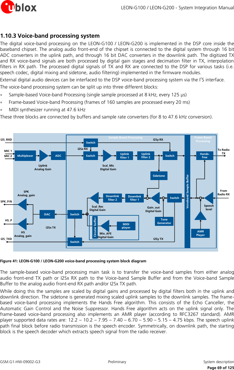
![LEON-G100 / LEON-G200 - System Integration Manual GSM.G1-HW-09002-G3 Preliminary System description Page 70 of 125 The circular buffer is a 3000 word buffer to store and mix the voice-band samples from Midi synthesizer. The buffer has a circular structure, so that when the write pointer reaches the end of the buffer, it is wrapped to the begin address of the buffer. Two different sample-based sample rate converters are used: an interpolator, required to convert the sample-based voice-band processing sampling rate of 8 kHz to the analog audio front-end output rate of 47.6 kHz; a decimator, required to convert the circular buffer sampling rate of 47.6 kHz to the I2Sx TX or the uplink path sample rate of 8 kHz. 1.10.3.1 Audio codecs The following speech codecs are supported by firmware on the DSP: GSM Half Rate (TCH/HS) GSM Full Rate (TCH/FS) GSM Enhanced Full Rate (TCH/EFR) 3GPP Adaptive Multi Rate (AMR) (TCH/AFS+TCH/AHS) 1.10.3.2 Echo cancelation and noise reduction LEON-G100 / LEON-G200 support algorithms for echo cancellation, noise suppression and automatic gain control. Algorithms are configurable with AT commands (refer to the u-blox AT Commands Manual [2]). 1.10.3.3 Digital filters and gains Audio parameters such as digital filters, digital gain, Side-tone gain (feedback from uplink to downlink path) and analog gain are available for uplink and downlink audio paths. These parameters can be modified by dedicated AT commands and be saved in 2 customer profiles in the non-volatile memory of the module (refer to the u-blox AT Commands Manual [2]). 1.10.3.4 Ringer mode LEON-G100 / LEON-G200 modules support polyphonic ring tones. The ringer tones are generated by a built-in generator on the chipset and then amplified by the internal amplifier. The synthesizer output is only mono and cannot be mixed with TCH voice path (the two are mutually exclusive). To perform in-band alerting during TCH with voice path open, only Tone Generator can be used. The analog audio path used in ringer mode can be the high power differential audio output (refer to u-blox AT Commands Manual [2]; AT+USPM command, <main_downlink> and <alert_sound> parameters for alert sounds routing). In this case the external high power loudspeaker must be connected to the SPK_P/SPK_N output pins of the module as shown in the application circuit (Figure 38) described in section 1.10.1.5. 1.11 ADC input (LEON-G100 only) One Analog to Digital Converter input is available (ADC1) and is configurable using u-blox AT command (see u-blox AT Commands Manual [2]). The resolution of this converter is 12-bit with a single ended input range. Name Description Remarks ADC1 ADC input Resolution: 12 bits. Table 27: ADC pin ADC1 pin ESD sensitivity rating is 1 kV (HBM JESD22-A114F). A higher protection level could be required if the line is externally accessible on the application board. A higher protection level can be achieved mounting an ESD protection (e.g. EPCOS CA05P4S14THSG varistor array) on the line connected to this pin if it is externally accessible on the application board.](https://usermanual.wiki/TransCore/2000B.User-Manual-I/User-Guide-2324779-Page-70.png)
![LEON-G100 / LEON-G200 - System Integration Manual GSM.G1-HW-09002-G3 Preliminary System description Page 71 of 125 If the ADC1 pin is not used, it can be left floating on the application board. The electrical behavior of the measurement circuit in voltage mode can be modeled by a circuit equivalent to that shown in Figure 42. This includes a resistor (Req), voltage source (Ueq), analog preamplifier (with typical gain G=0.5), and a digital amplifier (with typical gain gADC=2048 LSB/V). LEON-G100ADC1UeqReqUsigRsigUadcG5gADC Figure 42: Equivalent network for ADC single-ended measurement The ADC software driver takes care of the parameters shown in Figure 42 (Req, Ueq, G, gADC): the voltage measured by ADC1 is Uadc and its value expressed in mV is given by the AT+UADC=0 response (for more details on the AT command refer to u-blox AT Commands Manual [2]). The detailed electrical specifications of the Analog to Digital Converter input (Input voltage span, Input resistance in measurement mode Req, Internal voltage Ueq): are reported in the LEON-G100 / LEON-G200 Data Sheet [1]. As described in the ADC equivalent network shown in Figure 42, one part of the whole ADC circuit is outside the module: the (Usig) and the (Rsig) are characteristics of the application board because they represent the Thévenin's equivalent of the electrical network developed on the application board. If an external voltage divider is implemented to increase the voltage range, check the input resistance in measurement mode (Req) of ADC1 input and all the electrical characteristics. If the Thévenin's equivalent of the voltage source (Usig) has a significant internal resistance (Rsig) compared to the input resistance in measurement mode (Req) of the ADC, this should be taken into account and corrected to properly associate the AT+UADC=0 response to the voltage source value, implementing the ADC calibration procedure suggested in the section 1.11.1 below. If the customer implements the calibration procedure on the developed application board, the influence of the internal series resistance (Rsig) of the voltage source (Usig) is taken into account in the measurement: the AT+UADC=0 response can be correctly associated to the value of the voltage source applied on the application board. 1.11.1 ADC Calibration To improve the absolute accuracy of the 12-bit analog-to-digital converter (ADC), it is suggested to follow the calibration procedure here described. The calibration aim is to evaluate the relationship between the value, expressed in mV, of the voltage source (V_S, which Thévenin's equivalent is represented by Usig and Rsig shown in Figure 42) that has to be measured and the AT+UADC=0 response (ADC_VALUE, that is the Uadc value expressed in mV) when V_S is applied, calculating the calibration GAIN and OFFSET parameters value.](https://usermanual.wiki/TransCore/2000B.User-Manual-I/User-Guide-2324779-Page-71.png)
![LEON-G100 / LEON-G200 - System Integration Manual GSM.G1-HW-09002-G3 Preliminary System description Page 73 of 125 1.12 General Purpose Input/Output (GPIO) LEON-G100 / LEON-G200 modules provide some pins which can be configured as general purpose input or output, or to provide special functions via u-blox AT commands (for further details refer to u-blox AT Commands Manual [2], AT+UGPIOC, AT+UGPIOR, AT+UGPIOW, AT+UGPS, AT+UGPRF, AT+USPM). The number of available general purpose input/output pins and the special functions availability can vary depending on the LEON-G100 / LEON-G200 ordering code. For each pin the GPIO configuration is saved in the non volatile memory. For more details refer to u-blox AT commands manual [2]. 1.12.1 LEON-G100-06x / LEON-G200-06S and subsequent versions LEON-G100-06x / LEON-G200-06S and subsequent versions provide 5 general purpose input/output pins: GPIO1, GPIO2, GPIO3, GPIO4, HS_DET. The available functions are described below: GPS supply enable: GPIO2 is by default configured by AT+UGPIOC command to enable or disable the supply of the u-blox GPS receiver connected to the wireless module. The GPIO1, GPIO3, GPIO4 or HS_DET pins can be configured to provide the “GPS supply enable” function, alternatively to the default GPIO2 pin, setting the parameter <gpio_mode> of AT+UGPIOC command to 3. The pin configured to provide the “GPS supply enable” function is set as o Output / High, to switch on the u-blox GPS receiver, if the parameter <mode> of AT+UGPS command is set to 1 o Output / Low, to switch off the u-blox GPS receiver, if the parameter <mode> of AT+UGPS command is set to 0 (default setting) The pin configured to provide the “GPS supply enable” function must be connected to the active-high enable pin (or the active-low shutdown pin) of the voltage regulator that supplies the u-blox GPS receiver on the application board. GPS data ready: GPIO3 is by default configured by AT+UGPIOC command to sense when the u-blox GPS receiver connected to the wireless module is ready to send data by the DDC (I2C) interface. Only the GPIO3 pin can be configured to provide the “GPS data ready” function, setting the parameter <gpio_mode> of AT+UGPIOC command to 4 (default setting). The pin configured to provide the “GPS data ready” function is set as o Input, to sense the line status, waking up the wireless module from idle-mode when the u-blox GPS receiver is ready to send data by the DDC (I2C) interface, if the parameter <mode> of AT+UGPS command is set to 1 and the parameter <GPS_IO_configuration> of AT+UGPRF command is set to 16 o Tri-state with an internal active pull-down enabled, otherwise (default setting) The pin must be connected to the data ready output of the u-blox GPS receiver (i.e. the pin TxD1 of the u-blox GPS receiver) on the application board. GPS RTC sharing: GPIO4 is by default configured by AT+UGPIOC command to provide a synchronization timing signal to the u-blox GPS receiver connected to the wireless module. Only the GPIO4 pin can be configured to provide the “GPS RTC sharing” function, setting the parameter <gpio_mode> of AT+UGPIOC command to 5 (default setting). The pin configured to provide the “GPS RTC sharing” function is set as](https://usermanual.wiki/TransCore/2000B.User-Manual-I/User-Guide-2324779-Page-73.png)
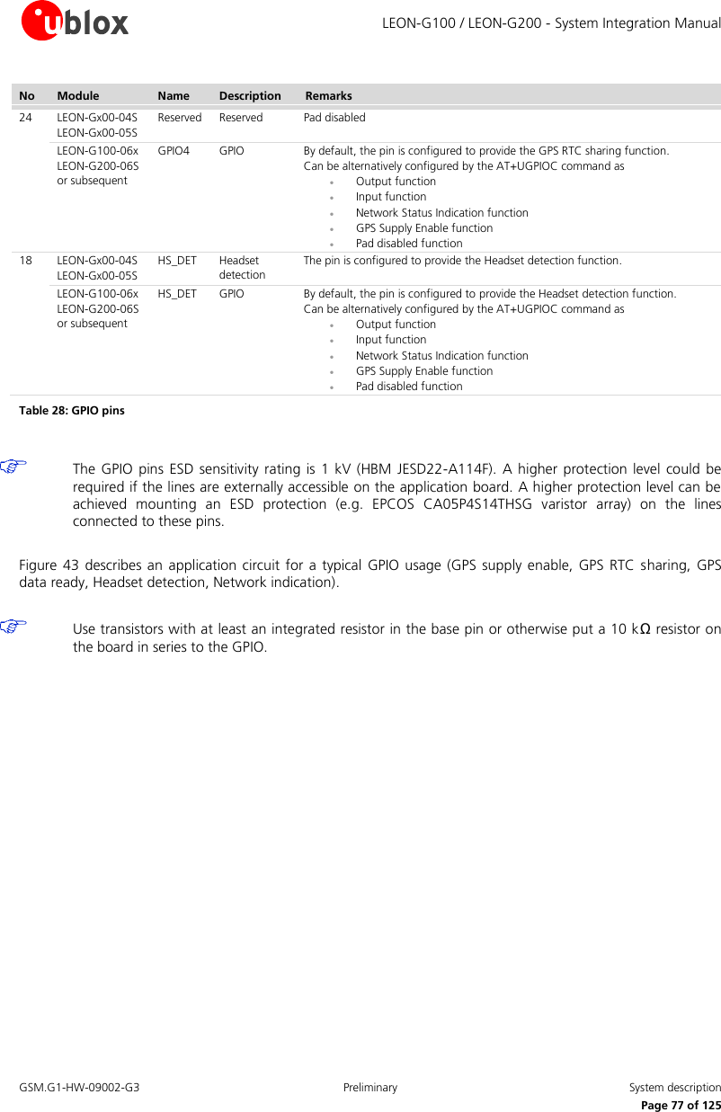
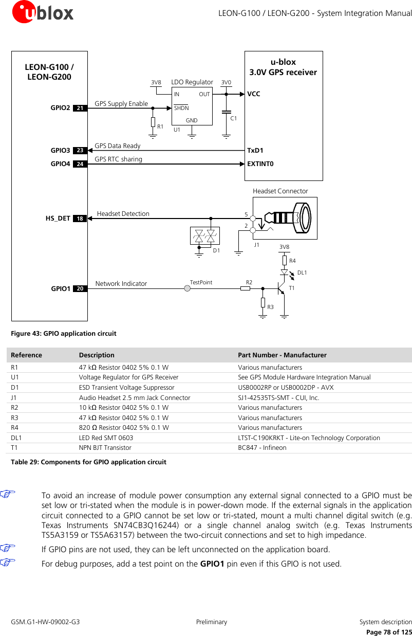
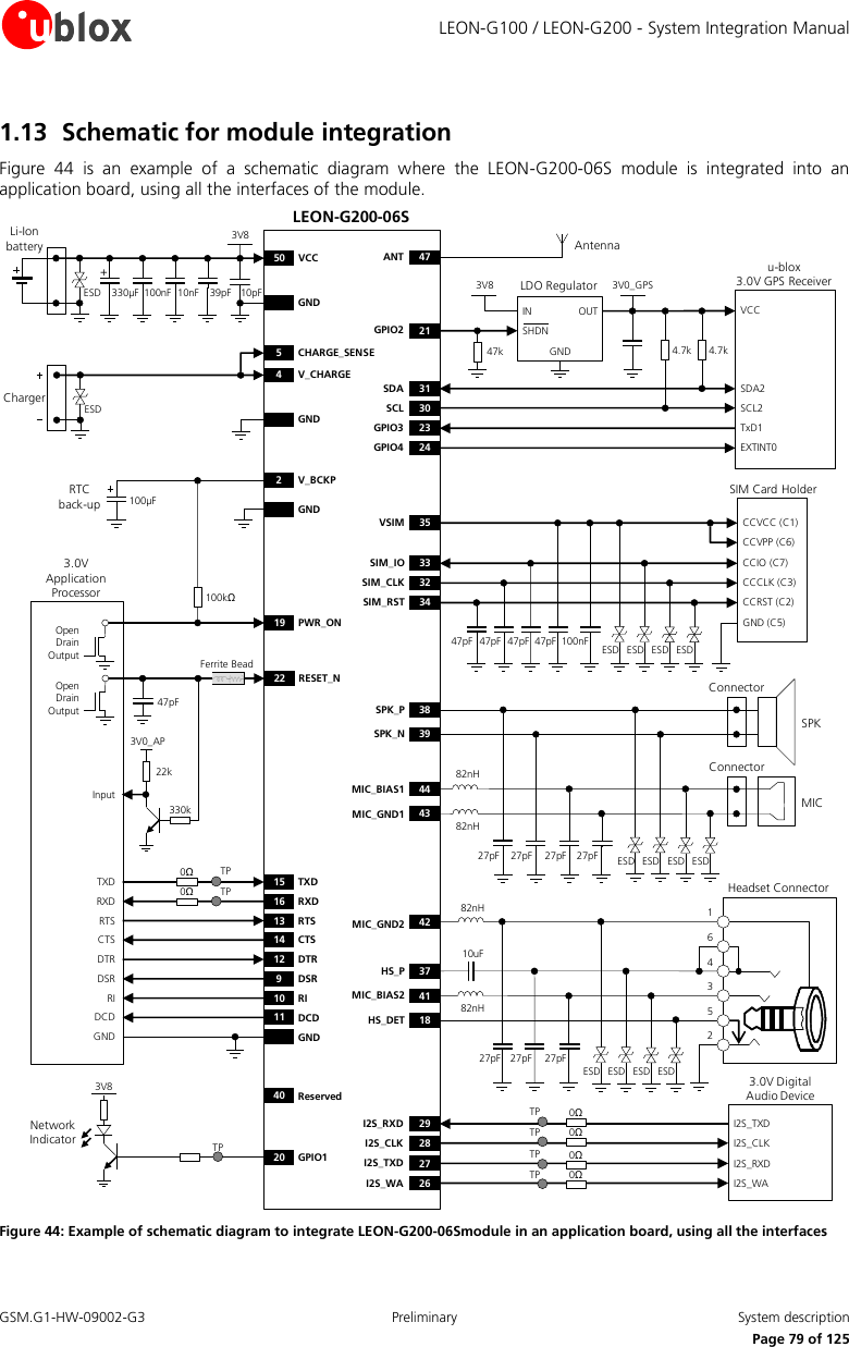
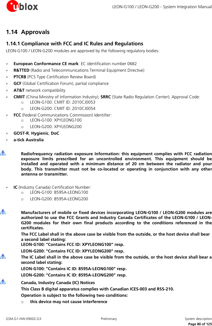
![LEON-G100 / LEON-G200 - System Integration Manual GSM.G1-HW-09002-G3 Preliminary Design-In Page 83 of 125 2 Design-In 2.1 Design-in checklist This section provides a design-in checklist. 2.1.1 Schematic checklist The following are the most important points for a simple schematic check: DC supply must provide a nominal voltage at VCC pin above the minimum normal operating range limit. DC supply must be capable to provide 2.5 A current bursts with maximum 400 mV voltage drop at VCC pin. VCC supply should be clean, with very low ripple/noise: suggested passive filtering parts can be inserted. Connect only one DC supply to VCC: different DC supply systems are mutually exclusive. V_CHARGE and CHARGE_SENSE must be externally shorted (LEON-G200 only). The DC supply used as charger must be voltage and current limited as specified (LEON-G200 only). Do no leave PWR_ON floating: add a pull-up resistor to a proper supply (i.e. V_BCKP). Check that voltage level of any connected pin does not exceed the relative operating range. Capacitance and series resistance must be limited on each SIM signal to match the SIM specifications. Insert the suggested low capacitance ESD protection and passive filtering parts on each SIM signal. Check UART signals direction, since the signal names follow the ITU-T V.24 Recommendation [4]. Add a proper pull-up resistor to a proper supply on each DDC (I2C) interface line, if the interface is used. Capacitance and series resistance must be limited on each line of the DDC (I2C) interface. Insert the suggested passive filtering parts on each used analog audio line. Check the digital audio interface specifications to connect a proper device. For debug purposes, add a test point on each I2S pin and on GPIO1 also if they are not used. Use transistors with at least an integrated resistor in the base pin or otherwise put a 10 kΩ resistor on the board in series to the GPIO when those are used to drive LEDs. To avoid an increase of module current consumption in power down mode, any external signals connected to the module digital pins (UART interface, HS_DET, GPIOs) must be set low or tri-stated when the module is in power down mode. Any external signal connected to the UART interface, I2S interfaces and GPIOs must be tri-stated when the module is in power-down mode, when the external reset is forced low and during the module power-on sequence (at least for 3 s after the start-up event), to avoid latch-up of circuits and let a proper boot of the module. Provide proper precautions for ESD immunity as required on the application board. All the not used pins can be left floating on the application board. 2.1.2 Layout checklist The following are the most important points for a simple layout check: Check 50 Ω impedance of ANT line. Follow the recommendations of the antenna producer for correct antenna installation and deployment (PCB layout and matching circuitry). Ensure no coupling occurs with other noisy or sensitive signals (primarily MIC signals, audio output signals, SIM signals). VCC line should be wide and short.](https://usermanual.wiki/TransCore/2000B.User-Manual-I/User-Guide-2324779-Page-83.png)
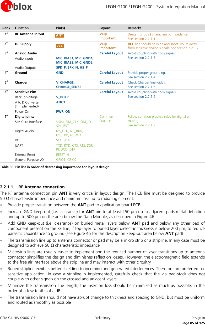
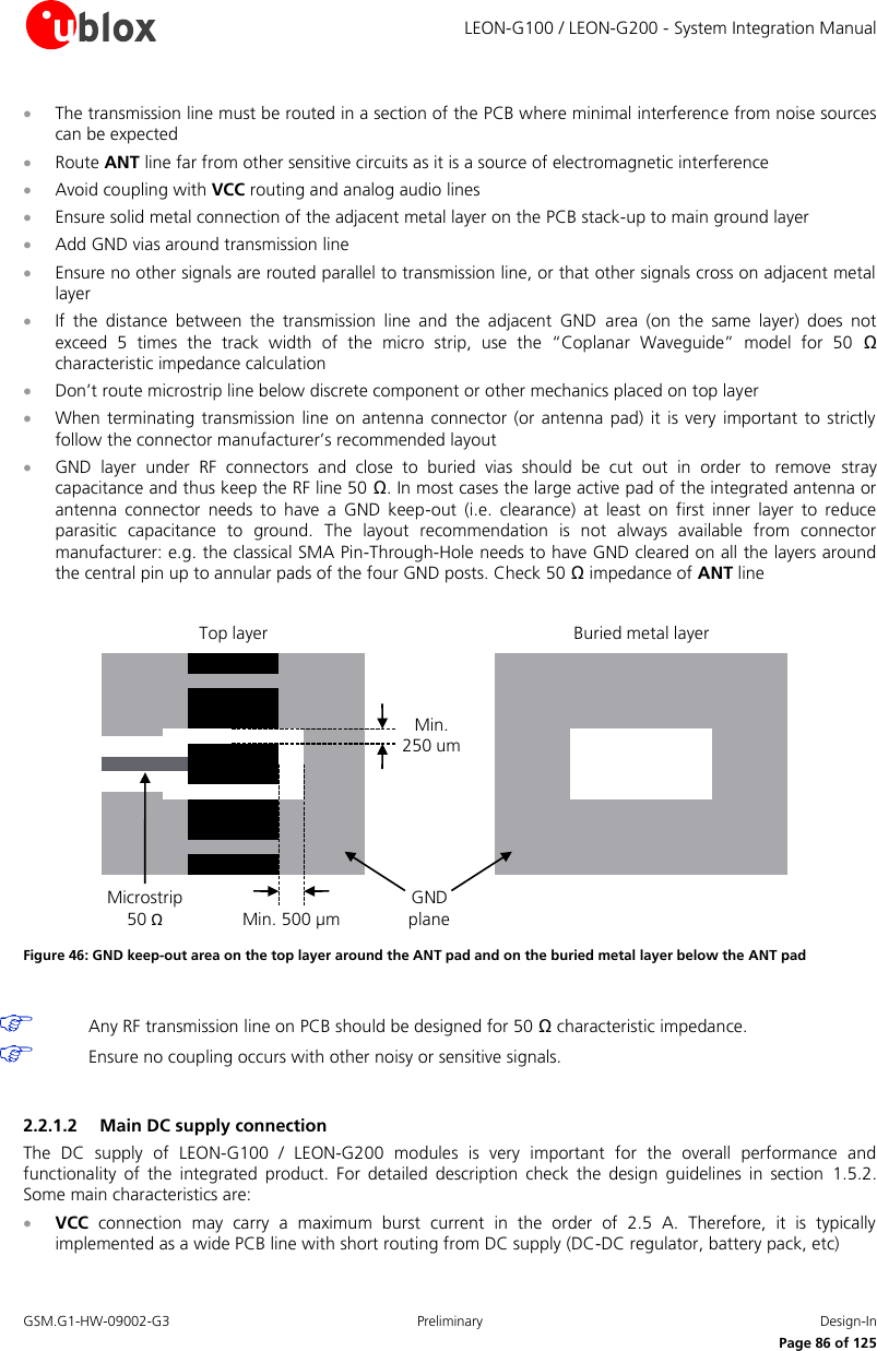
![LEON-G100 / LEON-G200 - System Integration Manual GSM.G1-HW-09002-G3 Preliminary Design-In Page 90 of 125 2.2.2 Footprint and paste mask Figure 47 and Figure 48 describe the footprint and provide recommendations for the paste mask for LEON modules. These are recommendations only and not specifications. The copper and solder masks have the same size and position. 29.5 mm [1161.4 mil]18.9 mm [744.1 mil]0.8 mm [31.5 mil]1.1 mm [43.3 mil]1.55 mm [61.0 mil]1.0 mm [39.3 mil] 0.8 mm [31.5 mil] Figure 47: LEON-G100 / LEON-G200 footprint 21.3 mm [838.6 mil]18.9 mm [744.1 mil]Stencil: 120 µm17.1 mm [673.2 mil]0.6 mm [23.6 mil]0.8 mm [31.5 mil] Figure 48: LEON-G100 / LEON-G200 paste mask To improve the wetting of the half vias, reduce the amount of solder paste under the module and increase the volume outside of the module by defining the dimensions of the paste mask to form a T-shape (or equivalent) extending beyond the Copper mask. The solder paste should have a total thickness of 120 µm. The paste mask outline needs to be considered when defining the minimal distance to the next component. The exact geometry, distances, stencil thicknesses and solder paste volumes must be adapted to the specific production processes (e.g. soldering etc.) of the customer. The bottom layer of LEON-G100 / LEON-G200 shows some unprotected copper areas for GND and VCC signals, plus GND keep-out for internal RF signals routing. Consider “No-routing” areas for the LEON-G100 / LEON-G200 footprint as follows: 1. Ground copper and signals keep-out below LEON-G100 / LEON-G200 on Application Motherboard due to VCC area, RF ANT pin and exposed GND pad on module bottom layer (see Figure 49). 2. Signals Keep-Out below module on Application Motherboard due to GND opening on LEON-G100 / LEON-G200 bottom layer for internal RF signals (see Figure 50).](https://usermanual.wiki/TransCore/2000B.User-Manual-I/User-Guide-2324779-Page-90.png)
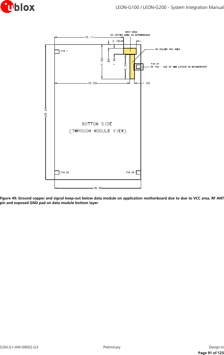
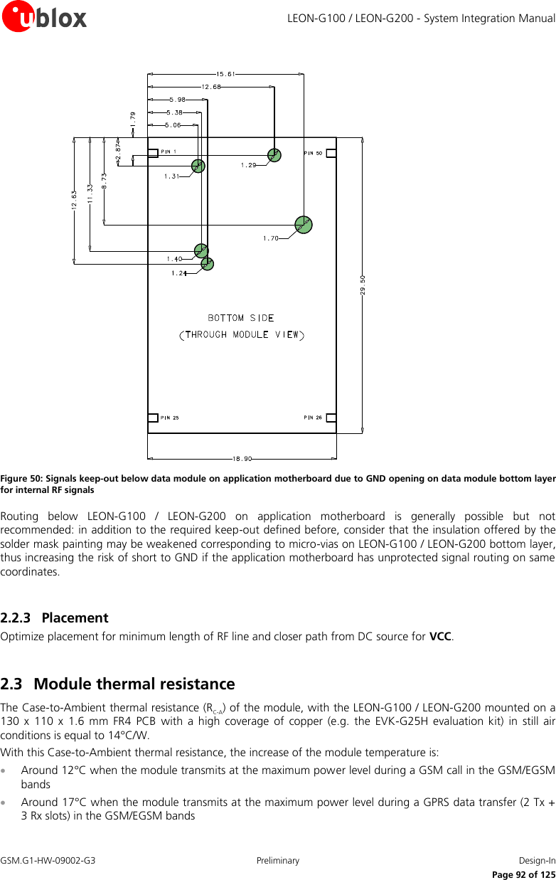
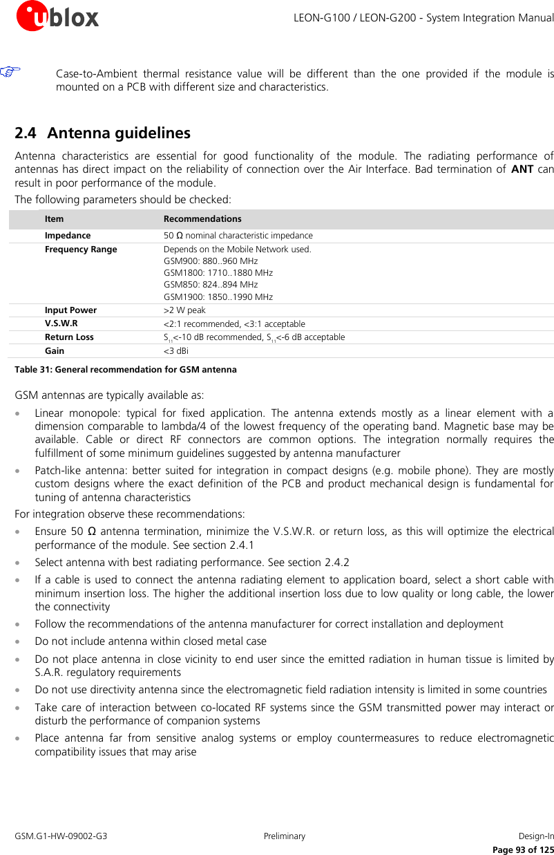
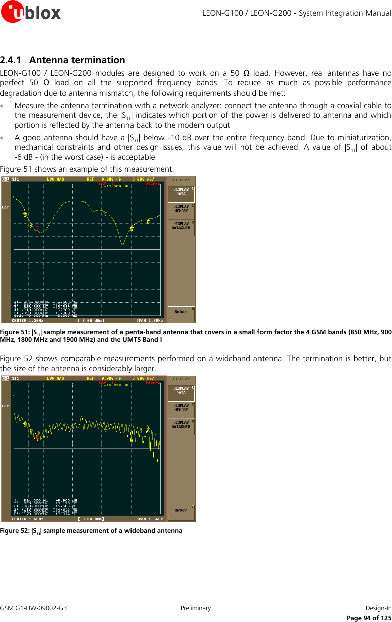
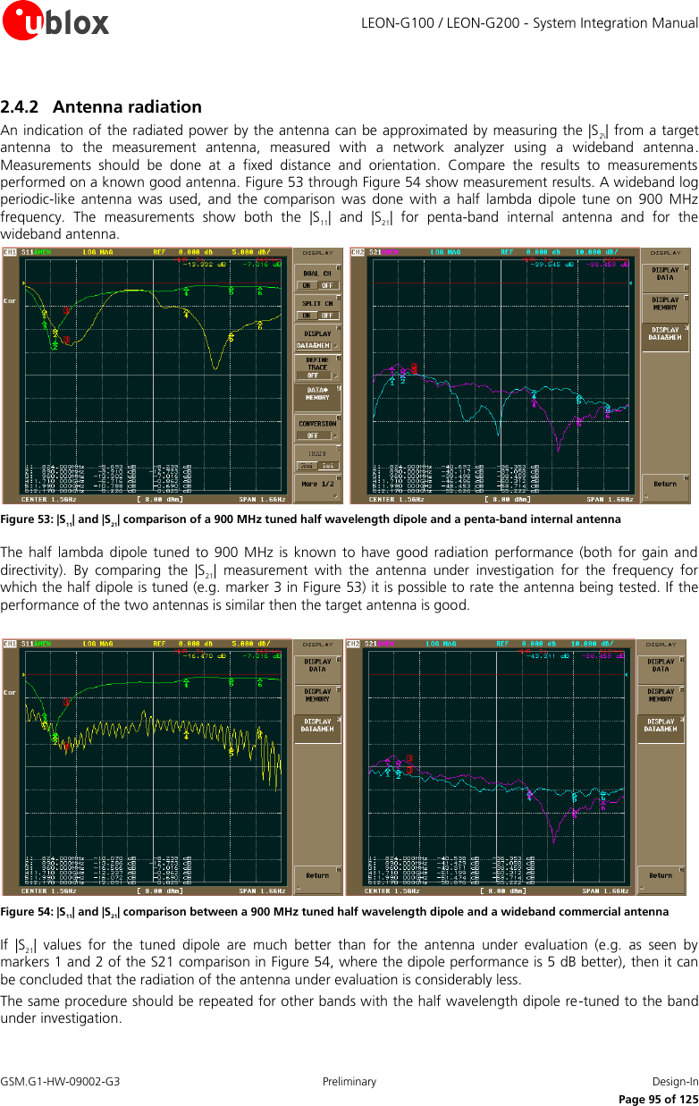
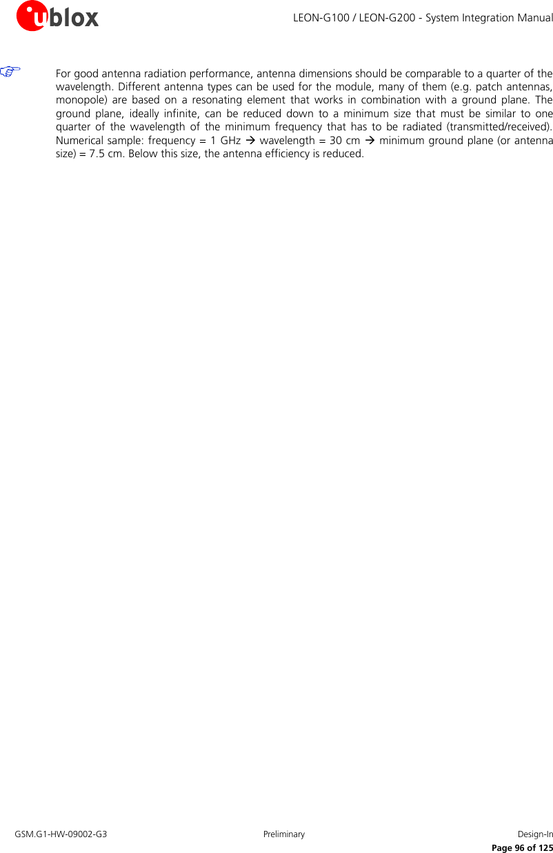
![LEON-G100 / LEON-G200 - System Integration Manual GSM.G1-HW-09002-G3 Preliminary Design-In Page 97 of 125 2.4.3 Antenna detection functionality The internal antenna detect circuit is based on ADC measurement at ANT pin: the RF port is DC coupled to the ADC unit in the baseband chip which injects a DC current (30 µA for 250 µs) on ANT and measures the resulting DC voltage to evaluate the resistance from ANT pad to GND. The antenna detection is performed by the measurement of the resistance from ANT pad to GND (DC element of the GSM antenna), that is forced by the AT+UANTR command: refer to u-blox AT Commands Manual [2] for more details on how to access to this feature. To achieve good antenna detection functionality, use an RF antenna with built-in resistor from ANT signal to GND, or implement an equivalent solution with a circuit between the antenna cable connection and the radiating element as shown in Figure 55. Antenna AssemblyDiagnostic CircuitApplication BoardLEON-G100/G200ANTADCCurrent SourceRF ChokeDC BlockingFront-End RF ModuleRF ChokeDC BlockingRadiating ElementZo=50 OhmResistor for DiagnosticCoaxial Antenna CableInternal Resistor Figure 55: Module Antenna Detection circuit and antenna with diagnostic resistor Examples of components for the antenna detection diagnostic circuit are reported in the following table: Description Part Number - Manufacturer DC Blocking Capacitor Murata GRM1555C1H220JA01 or equivalent RF Choke Inductor Murata LQG15HS68NJ02, LQG15HH68NJ02 or equivalent Resistor for Diagnostic 15kΩ 5%, various Manufacturers Table 32: Example of components for the antenna detection diagnostic circuit The DC impedance at RF port for some antennas may be a DC open (e.g. linear monopole) or a DC short to reference GND (e.g. PIFA antenna). For those antennas, without the diagnostic circuit Figure 55, the measured DC resistance will be always on the extreme of measurement range (respectively open or short), and there will be no mean to distinguish from defect on antenna path with similar characteristic (respectively: removal of linear antenna or RF cable shorted to GND for PIFA antenna). Furthermore, any other DC signal injected to the RF connection from ANT connector to radiating element will alter the measurement and produce invalid results for antenna detection.](https://usermanual.wiki/TransCore/2000B.User-Manual-I/User-Guide-2324779-Page-97.png)
![LEON-G100 / LEON-G200 - System Integration Manual GSM.G1-HW-09002-G3 Preliminary Design-In Page 99 of 125 2.5 ESD Immunity Test Precautions The immunity of the device (i.e. the application board where LEON module is mounted) to the EMS phenomenon Electrostatic Discharge must be certified in compliance to the testing requirements standard [9] and the requirements for radio and digital cellular radio telecommunications system equipment standards [10] [11]. The ESD test is performed at the enclosure port [10] referred to as the physical boundary through which the EM field radiates. If the device implements an integral antenna [10] the enclosure port is seen as all insulating and conductive surfaces housing the device. If the device implements a removable antenna [10], the antenna port [10] can be separated from the enclosure port. The antenna port comprises the antenna element and its interconnecting cable surfaces. The applicability of the ESD test depends to the device classification [10], as well the test on other ports [10] or on interconnecting cables to auxiliary equipments depends to the device accessible interfaces and manufacturer requirements. Contact discharges [9] are performed at conductive surfaces whereas air discharges [9] are performed at insulating surfaces. Indirect contact discharges are performed to the measurement setup horizontal and vertical coupling planes [9]. Implement the following precautions to satisfy ESD immunity test requirements [9] [10] [11] performed at the device enclosure in compliance to the category level [10] and shown in Table 33. Application Category Immunity Level All exposed surfaces of the radio equipment and ancillary equipment in a representative configuration Contact Discharge 4 kV Air Discharge 8 kV Table 33: Electromagnetic Compatibility (EMC) ESD immunity requirement, standards “EN 61000-4-2, EN 301 489-1 V1.8.1, EN 301 489-7 V1.3.1” Although EMC certification (including ESD immunity testing) must be performed in the final application of the radio equipment EUT, results are provided for LEON modules performing the test with a representative configuration to show that requirements can be met. The reference application design consists of a LEON soldered onto a motherboard which provides an interface to power supply, SIM card, headset, and communication port. GSM external antenna in connected to SMA connector provided on the motherboard. Since an external antenna is used, the antenna port can be separated from the enclosure port. The reference application is not enclosed in a box so the enclosure port is not identified with physical surfaces. Therefore, some test cases cannot be applied. Only the antenna port is identified as accessible for direct ESD exposure. The reference application implements all precautions described in the sections below. ESD immunity test results and applicability are reported in Table 34 according to test requirements [9] [10] [11].](https://usermanual.wiki/TransCore/2000B.User-Manual-I/User-Guide-2324779-Page-99.png)
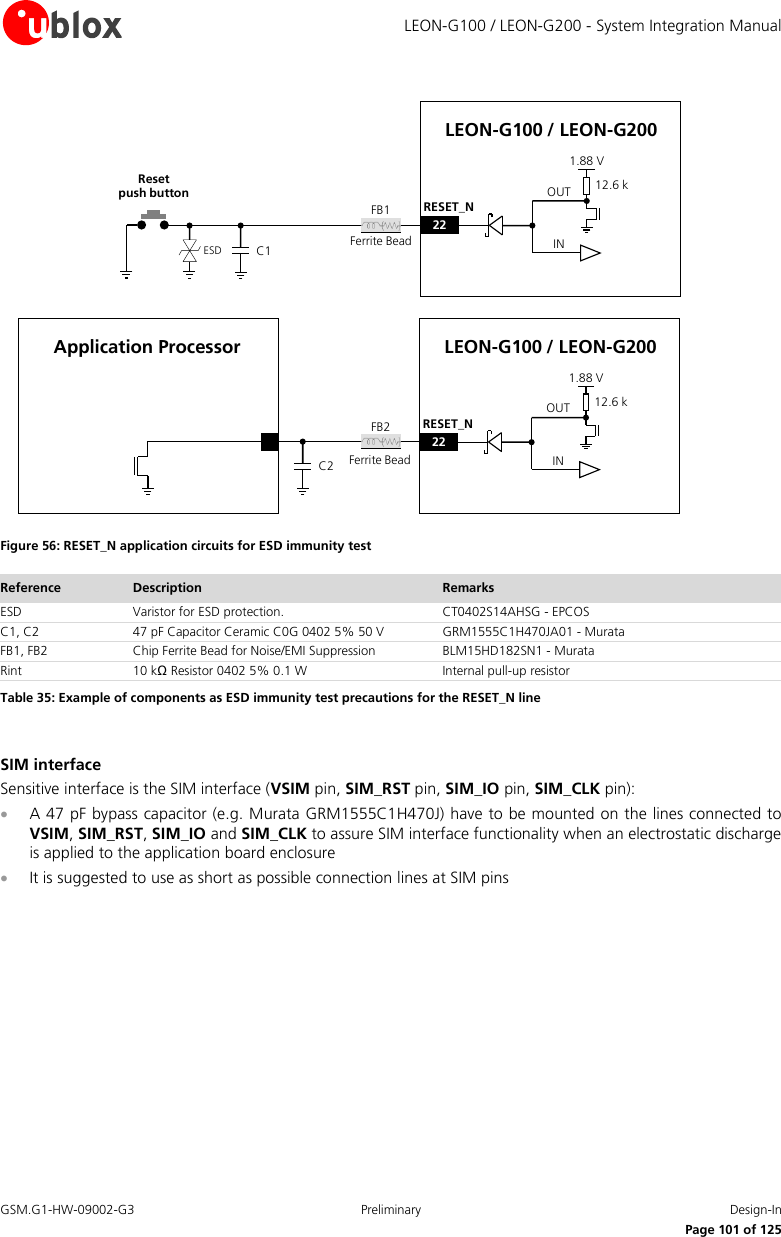
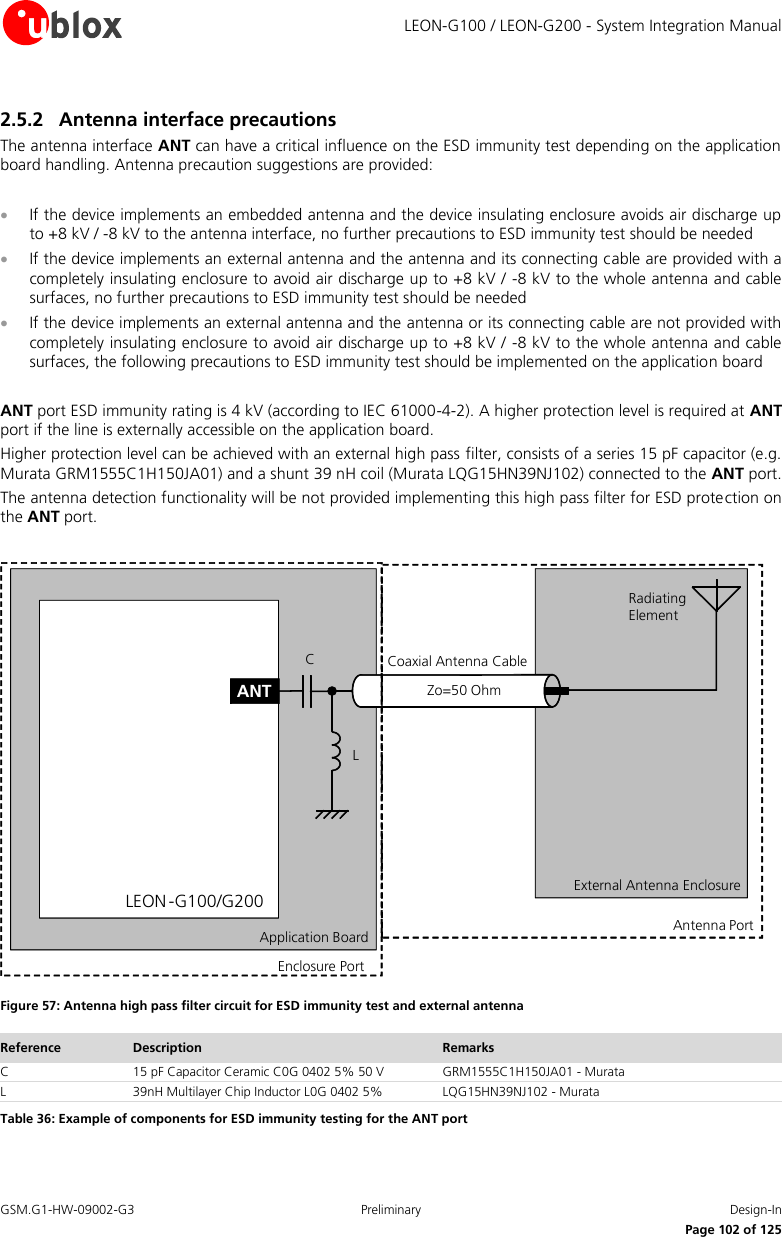
![LEON-G100 / LEON-G200 - System Integration Manual GSM.G1-HW-09002-G3 Preliminary Design-In Page 103 of 125 2.5.3 Module interfaces precautions All module pins that are externally accessible should be included in the ESD immunity test since they are considered to be a port [10]. Depending on applicability, and in order to satisfy ESD immunity test requirements and ESD category level, pins connected to the port should be protected up to +4 kV / -4 kV for direct Contact Discharge, and up to +8 kV / -8 kV for Air Discharge applied to the enclosure surface. The maximum ESD sensitivity rating of all the pins of the module, except the ANT pin, is 1 kV (Human Body Model according to JESD22-A114F). A higher protection level can be achieved by mounting an ESD protection (e.g. EPCOS CA05P4S14THSG varistor array). For the SIM interface a low capacitance (i.e. less than 10 pF) ESD protection (e.g. Infineon ESD8V0L2B-03L or AVX USB0002) must be placed near the SIM card holder on each line (VSIM, SIM_IO, SIM_CLK, SIM_RST).](https://usermanual.wiki/TransCore/2000B.User-Manual-I/User-Guide-2324779-Page-103.png)
![LEON-G100 / LEON-G200 - System Integration Manual GSM.G1-HW-09002-G3 Preliminary Feature description Page 104 of 125 3 Feature description 3.1 Firmware (upgrade) Over The Air (FOTA) (LEON-G200 only) LEON-G200 Firmware can be updated Over The Air. The main idea with updating Firmware over the air is to reduce the amount of data required for transmission to the LEON module. This is achieved by downloading only a “delta file” instead of the full Firmware. The delta contains only the differences between the two firmware versions (old and new), and is compressed. For more details refer to Firmware Update Application Note [13]. 3.2 Firmware (upgrade) Over AT (FOAT) Firmware upgrade is available with LEON-G100 / LEON-G200 modules using AT commands. 3.2.1 Overview This feature allows upgrade the module Firmware over UART, using AT Commands. AT Command AT+UFWUPD triggers a reboot and followed by upgrade procedure at specified baud rate (refer to u-blox AT Commands Manual [2] for more details) The Xmodem-1k protocol is used for downloading the new Firmware image via a terminal application A special boot loader on the module performs Firmware installation, security verifications and module reboot Firmware authenticity verification is performed via a security signature during the download. Firmware is then installed, overwriting the current version. In case of power loss during this phase, the boot loader detects a fault at the next wake-up, and restarts the Firmware download from the Xmodem-1k handshake. After completing the upgrade, the module is reset again and wakes-up in normal boot 3.2.2 FOAT procedure The application processor must proceed in the following way: send through the UART the AT+UFWUPD command, specifying the file type and the desired baud rate reconfigure the serial communication at the selected baud rate, without flow control with the Xmodem-1k protocol send the new FW image via Xmodem-1k 3.3 Firewall The feature allows the LEON-G100 / LEON-G200 user to reject incoming connections originated from IP addresses different from the specified list and inserted in a black list. 3.4 TCP/IP Via the AT commands it’s possible to access the TCP/IP functionalities over the GPRS connection. For more details about AT commands see the u-blox AT Commands Manual [2]. 3.4.1 Multiple IP addresses and sockets Using LEON’s embedded TCP/IP or UDP/IP stack, only 1 IP instance (address) is supported. The IP instance supports up to 16 sockets. Using an external TCP/IP stack (on the application processor), it is possible to have 3 IP instances (addresses). Comment [tgri2]: Is this not covered by the Application Note? Same as with previous,](https://usermanual.wiki/TransCore/2000B.User-Manual-I/User-Guide-2324779-Page-104.png)
![LEON-G100 / LEON-G200 - System Integration Manual GSM.G1-HW-09002-G3 Preliminary Feature description Page 105 of 125 3.5 FTP LEON-G100 / LEON-G200 modules support the File Transfer Protocol functionalities via AT commands. Files are read and stored in the local file system of the module. For more details about AT commands see the u-blox AT Commands Manual [2]. 3.6 HTTP HTTP client is implemented in LEON. HEAD, GET, POST, DELETE and PUT operations are available. The file size to be uploaded / downloaded depends on the free space available in the local file system (FFS) at the moment of the operation. Up to 4 HTTP client contexts to be used simultaneously. For more details about AT commands see the u-blox AT Commands Manual [2]. 3.7 SMTP LEON-G100 / LEON-G200 modules supports SMTP client functionalities. It is possible to specify the common parameters (e.g. server data, authentication method, etc.) can be specified, to send an email to a SMTP server. Emails can be sent with or without attachment. Attachments are store in the local module file system. For more details about AT commands see the u-blox AT Commands Manual [2]. 3.8 GPS The LEON-G100 / LEON-G200 modules allow a simple and fast connection with the u-blox GPS modules (u-blox 5 family and above). Via the DDC bus it’s possible to communicate and exchange data, while the available GPIOs can handle the GPS device power on/off. For information about implementing u-blox GPS with LEON-G100 / LEON-G200 modules, including using u-blox’ AssistNow Assisted GPS (A-GPS) service see the GPS Integration Application Note [3]. 3.9 Jamming detection In real network situations modules can experience various kind of out-of-coverage conditions: limited service conditions when roaming to networks not supporting the specific SIM, limited service in cells which are not suitable or barred due to operators’ choices, no cell condition when moving to poorly served or highly interfered areas. In the latter case, interference can be artificially injected in the environment by a noise generator covering a given spectrum, thus obscuring the operator’s carriers entitled to give access to the GSM service. The Jamming Detection Feature detects such “artificial” interference and reports the start and stop of such condition to the client, which can react appropriately by e.g. switching off the radio transceiver in order to reduce the power consumption and monitoring the environment at constant periods. The feature consists in detecting, at radio resource level, an anomalous source of interference and signaling it to the client with an unsolicited indication when the detection is entered or released. The jamming condition occurs when: The module has lost synchronization with the serving cell and cannot select any other cell The band scan reveals at least n carriers with power level equal or higher than threshold On all such carriers, no synchronization is possible The number of minimum disturbing carriers and the power level threshold can be configured by the client by using the AT+UCD command [2]. The jamming condition is cleared when any of the above mentioned statements does not hold. The congestion (i.e. jamming) detection feature can be enabled and configured by the +UCD AT command (for more details refer to the u-blox AT Commands Manual [2]).](https://usermanual.wiki/TransCore/2000B.User-Manual-I/User-Guide-2324779-Page-105.png)
![LEON-G100 / LEON-G200 - System Integration Manual GSM.G1-HW-09002-G3 Preliminary Feature description Page 106 of 125 3.10 Smart Temperature Management Wireless modules – independent of the specific model –always have a well defined operating temperature range. This range should be respected to guarantee full device functionality and long life span. Nevertheless there are environmental conditions that can affect operating temperature, e.g. if the device is located near a heating/cooling source, if there is/isn’t air circulating, etc. The module itself can also influence the environmental conditions; such as when it is transmitting at full power. In this case its temperature increases very quickly and can raise the temperature nearby. The best solution is always to properly design the system where the module is integrated. Nevertheless an extra check/security mechanism embedded into the module is a good solution to prevent operation of the device outside of the specified range. Smart Temperture Management feauture is not supported by LEON-Gx00-05S and previous versions. 3.10.1 Smart Temperature Supervisor (STS) The Smart Temperature Supervisor is activated and configured by a dedicated AT+USTS command. For more details refer to u-blox AT Commands Manual [2]. The wireless module measures the internal temperature (Ti) and its value is compared with predefined thresholds to identify the actual working temperature range. Temperature measurement is done inside the wireless module: the measured value could be different from the environmental temperature (Ta). Warningareat-1 t+1 t+2t-2Valid temperature rangeSafeareaDangerousarea Dangerousarea Warningarea Figure 58: Temperature range and limits The entire temperature range is divided into sub-regions by limits (see Figure 58) named t-2, t-1, t+1 and t+2. Within the first limit, (t-1 < Ti < t+1), the wireless module is in the normal working range, the Safe Area In the Warning Area, (t-2 < Ti < t.1) or (t+1 < Ti < t+2), the wireless module is still inside the valid temperature range, but the measured temperature approaches the limit (upper or lower). The module sends a warning to the user (through the active AT communication interface), which can take, if possible, the necessary actions to return to a safer temperature range or simply ignore the indication. The module is still in a valid and good working condition Outside the valid temperature range, (Ti < t-2) or (Ti > t+2), the device is working outside the specified range represents a dangerous working condition. This condition is indicated and the device shuts down to avoid damage For security reasons the shutdown is suspended in case an emergency call in progress. In this case the device will switch off at call termination. The user can decide at anytime to enable/disable the Smart Temperature Supervisor feature. If the feature is disabled there is no embedded protection against disallowed temperature conditions.](https://usermanual.wiki/TransCore/2000B.User-Manual-I/User-Guide-2324779-Page-106.png)
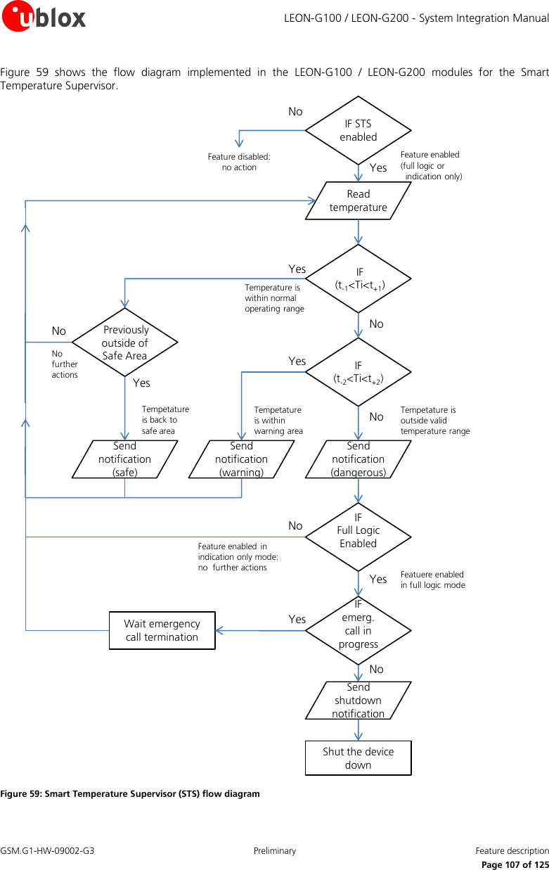
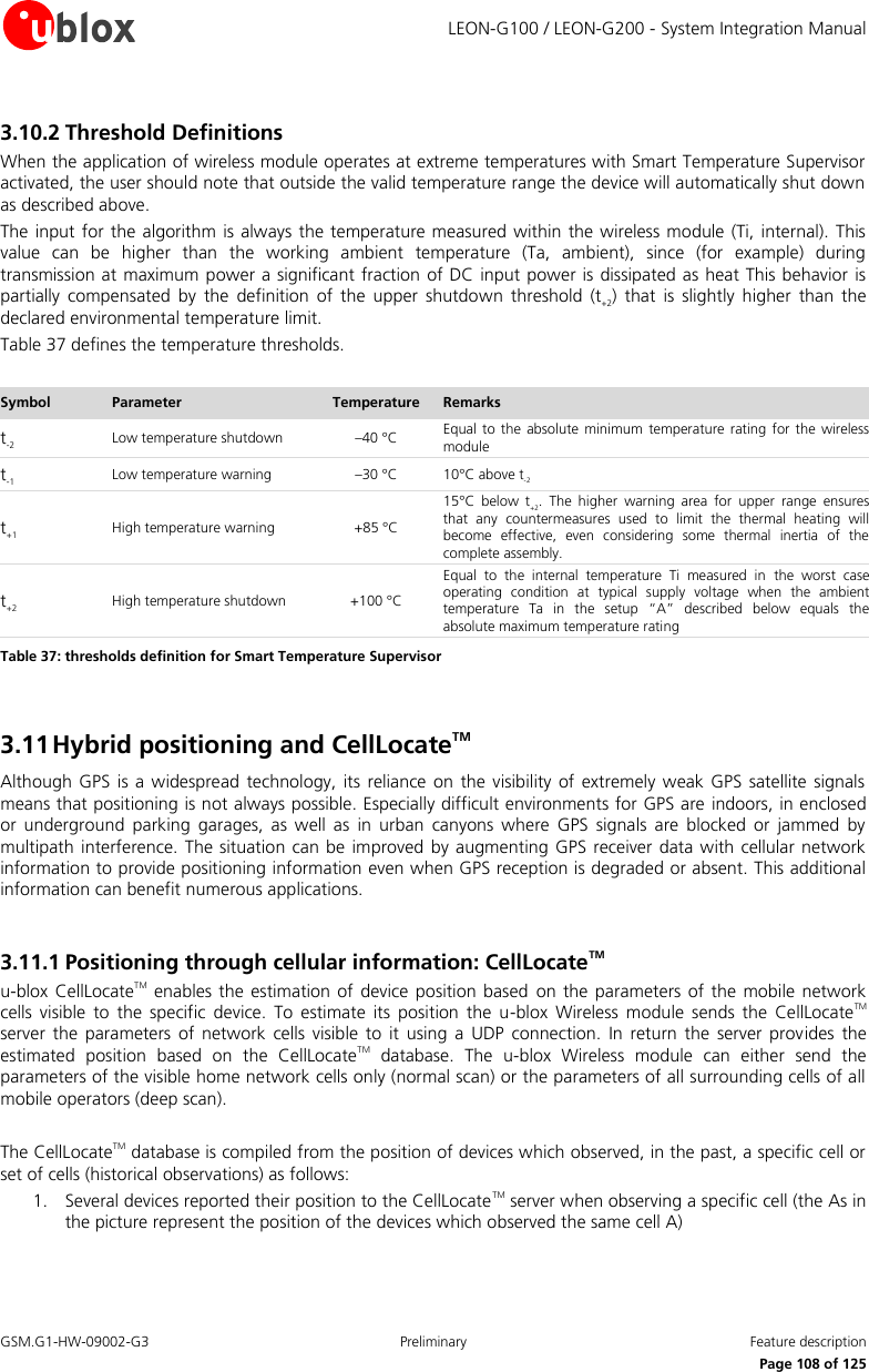
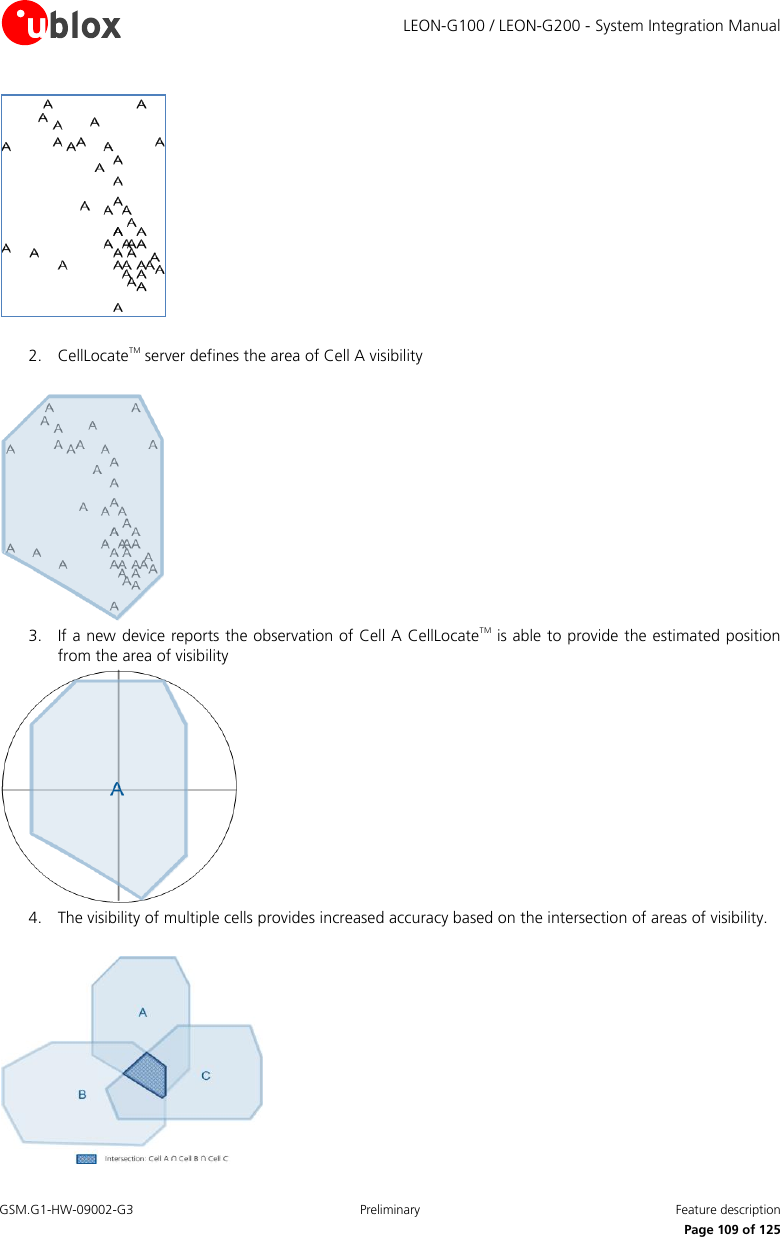
![LEON-G100 / LEON-G200 - System Integration Manual GSM.G1-HW-09002-G3 Preliminary Feature description Page 110 of 125 CellLocateTM is implemented using a set of two AT commands that allow configuration of the CellLocateTM service (AT+ULOCCELL) and requesting position according to the user configuration (AT+ULOC). The answer is provided in the form of an unsolicited AT command including latitude, longitude and estimated accuracy. The accuracy of the position estimated by CellLocateTM depends on the availability of historical observations in the specific area. 3.11.2 Hybrid positioning With u-blox Hybrid positioning technology, u-blox Wireless devices can be triggered to provide their current position using either a u-blox GPS receiver or the position estimated from CellLocateTM. The choice depends on which positioning method provides the best and fastest solution according to the user configuration, exploiting the benefit of having multiple and complementary positioning methods. Hybrid positioning is implemented through a set of three AT commands that allow configuration of the GNSS receiver (AT+ULOCGNSS), configuration of the CellLocateTM service (AT+ULOCCELL), and requesting the position according to the user configuration (AT+ULOC). The answer is provided in the form of an unsolicited AT command including latitude, longitude and estimated accuracy (if the position has been estimated by CellLocateTM), and additional parameters if the position has been computed by the GNSS receiver. The configuration of mobile network cells does not remain static (e.g. new cells are continuously added or existing cells are reconfigured by the network operators). For this reason, when a Hybrid positioning method has been triggered and the GNSS receiver calculates the position, a database self-learning mechanism has been implemented so that these positions are sent to the server to update the database and maintain its accuracy. The use of hybrid positioning requires a connection via the DDC (I2C) bus between the LEON module and the u-blox GPS receiver (Refer to chapter 1.9.2). Refer to GPS application note [3] for the complete description of the feature. u-blox is extremely mindful of user privacy. When a position is sent to the CellLocateTM server u-blox is unable to track the SIM used or the specific device. CellLocate and Hybrid positioning features are not supported by LEON-G100-05S and LEON-G200-05S modules and previous versions.](https://usermanual.wiki/TransCore/2000B.User-Manual-I/User-Guide-2324779-Page-110.png)
![LEON-G100 / LEON-G200 - System Integration Manual GSM.G1-HW-09002-G3 Preliminary Handling and soldering Page 111 of 125 4 Handling and soldering No natural rubbers, no hygroscopic materials nor materials containing asbestos are employed. 4.1 Packaging, shipping, storage and moisture preconditioning For information pertaining to reels and tapes, Moisture Sensitivity levels (MSD), shipment and storage information, as well as drying for preconditioning see the LEON-G100 / LEON-G200 Data Sheet [1]. LEON-G100 / LEON-G200 modules are Electro-Static Discharge (ESD) sensitive devices. Ensure ESD precautions are implemented during handling of the module. 4.2 Soldering 4.2.1 Soldering paste Use of "No Clean" soldering paste is strongly recommended, as it does not require cleaning after the soldering process has taken place. The paste listed in the example below meets these criteria. Soldering Paste: OM338 SAC405 / Nr.143714 (Cookson Electronics) Alloy specification: Sn 95.5 / Ag 3.9 / Cu 0.6 (95.5% Tin / 0.6 % Silver / 0.6% Copper) 95.5% Sn / 4.0% Ag / 0.5% Cu (95.5% Tin / 4.0 % Silver / 0.5% Copper) Melting Temperature: 217°C Stencil Thickness: 120 µm for base boards The final choice of the soldering paste depends on the approved manufacturing procedures. The paste-mask geometry for applying soldering paste should meet the recommendations in section 2.2.2 The quality of the solder joints on the connectors (’half vias’) should meet the appropriate IPC specification. 4.2.2 Reflow soldering A convection type-soldering oven is strongly recommended over the infrared type radiation oven. Convection heated ovens allow precise control of the temperature and all parts will be heated up evenly, regardless of material properties, thickness of components and surface color. Consider the "IPC-7530 Guidelines for temperature profiling for mass soldering (reflow and wave) processes, published 2001". Preheat phase Initial heating of component leads and balls. Residual humidity will be dried out. This preheat phase will not replace prior baking procedures. Temperature rise rate: max 3°C/s If the temperature rise is too rapid in the preheat phase it may cause excessive slumping. Time: 60 – 120 s If the preheat is insufficient, rather large solder balls tend to be generated. Conversely, if performed excessively, fine balls and large balls will be generated in clusters.](https://usermanual.wiki/TransCore/2000B.User-Manual-I/User-Guide-2324779-Page-111.png)
![LEON-G100 / LEON-G200 - System Integration Manual GSM.G1-HW-09002-G3 Preliminary Handling and soldering Page 112 of 125 End Temperature: 150 - 200°C If the temperature is too low, non-melting tends to be caused in areas containing large heat capacity. Heating/ reflow phase The temperature rises above the liquidus temperature of 217°C. Avoid a sudden rise in temperature as the slump of the paste could become worse. Limit time above 217°C liquidus temperature: 40 - 60 s Peak reflow temperature: 245°C Cooling phase A controlled cooling avoids negative metallurgical effects (solder becomes more brittle) of the solder and possible mechanical tensions in the products. Controlled cooling helps to achieve bright solder fillets with a good shape and low contact angle. Temperature fall rate: max 4°C / s To avoid falling off, modules should be placed on the topside of the motherboard during soldering. The final soldering temperature chosen at the factory depends on additional external factors like choice of soldering paste, size, thickness and properties of the base board, etc. Exceeding the maximum soldering temperature in the recommended soldering profile may permanently damage the module. Preheat Heating Cooling[°C] Peak Temp. 245°C [°C]250 250Liquidus Temperature217 217200 20040 - 60 sEnd Temp.max 4°C/s150 - 200°C150 150max 3°C/s60 - 120 s100 Typical Leadfree 100Soldering Profile50 50050 100 150 200 250 300Elapsed time [s] Figure 60: Recommended soldering profile When soldering lead-free LEON-G100 / LEON-G200 modules in a leaded process, check the following temperatures: PB- Technology Soaktime: 40-80 s Time above Liquidus: 40-90 s Peak temperature: 225-235°C LEON-G100 / LEON-G200 modules must not be soldered with a damp heat process.](https://usermanual.wiki/TransCore/2000B.User-Manual-I/User-Guide-2324779-Page-112.png)

![LEON-G100 / LEON-G200 - System Integration Manual GSM.G1-HW-09002-G3 Preliminary Product Testing Page 116 of 125 Components assembly on the device; it should be verified that: o Communication with host controller can be established o The interfaces between module and device are working o Overall RF performance test of the device including antenna Dedicated tests can be implemented to check the device. For example, the measurement of module current consumption when set in a specified status can detect a short circuit if compared with a “Golden Device” result. Module AT commands is used to perform functional tests (communication with host controller, check SIM card interface, check communication between module and GPS, GPIOs, ADC input, etc.) and to perform RF performance tests. 5.2.1 ‘Go/No go’ tests for integrated devices A ‘Go/No go’ test is to compare the signal quality with a “Golden Device” in a position with excellent GSM network coverage and after having dialed a call (refer to u-blox AT Commands Manual [2], AT+CSQ command: <rssi>, <ber> parameters). These kind of test may be useful as a ‘go/no go’ test but not for RF performance measurements. This test is suitable to check the communication with host controller and SIM card, the audio and power supply functionality and verify if components at antenna interface are well soldered. 5.2.2 Functional tests providing RF operation The command used to perform these functional tests is not available on LEON-Gx00-05S and previous versions. Refer to u-blox AT Commands Manual [2], for AT+UTEST command syntax description. Refer to End user test Application Note [15], for AT+UTEST command user guide, limitations and examples of use. Overall RF performance test of the device including antenna can be performed with basic instruments like standard spectrum analyzer and signal generator using an AT interface and AT+UTEST command. The AT+UTEST command gives a simple interface to set the module in Rx and Tx test modes ignoring GSM signalling protocol. The command can set the module: To transmit in a single time slot a GSM burst in a specified channel and power level In receiving mode in a specified channel to returns the measured power level](https://usermanual.wiki/TransCore/2000B.User-Manual-I/User-Guide-2324779-Page-116.png)
![LEON-G100 / LEON-G200 - System Integration Manual GSM.G1-HW-09002-G3 Preliminary Product Testing Page 117 of 125 APPLICATION PROCESSORLEONSPECTRUMANALYZERAT COMMANDGSMANTENNAAPPLICATION BOARDAPPLICATION PROCESSORLEONSIGNAL GENERATORAT COMMANDAPPLICATION BOARDRF POWERRXRF POWERTXWIDEBAND ANTENNAGSMANTENNAWIDEBAND ANTENNA Figure 62: Setup with spectrum analyzer and signal generator for radiated measurement This feature allows the measurement of the transmitter and receiver power level to check components assembly related to the module antenna interface and to check other device interfaces from which depends the RF performance. To avoid module damage during transmitter test a quad-band GSM antenna or a 50 Ω termination must be connected to ANT pin. To avoid module damage during receiver test the maximum power level received at ANT pin must meet module specifications. It is suggested not to exceed power level -15 dBm at antenna input. The AT+UTEST command sets the module to emit RF power ignoring GSM signalling protocol. This emission can generate interference that can be prohibited by law in some countries. The use of this feature is intended for testing purpose in controlled environments by qualified user and must not be used during the normal module operation. Follow instructions suggested in u-blox documentation. u-blox assumes no responsibilities for the inappropriate use of this feature. Example of production tests for OEM manufacturer: 1. Trigger TX burst at low PCL (lower than 10) or trigger a RX measurement to check: o If ANT pin is soldered o If ANT pin is in short circuit o If module was damaged during soldering process or during handling (ESD, mechanical shock…) o If antenna matching components on application board are soldered o If integrated antenna is correctly connected Comment [tgri3]: This is a specification and belongs in the Data Sheet.](https://usermanual.wiki/TransCore/2000B.User-Manual-I/User-Guide-2324779-Page-117.png)
![LEON-G100 / LEON-G200 - System Integration Manual GSM.G1-HW-09002-G3 Preliminary Related documents Page 121 of 125 Related documents [1] u-blox LEON-G100 / LEON-G200 Data Sheet, Docu No GSM.G1-HW-10004 [2] u-blox AT Commands Manual, Docu No WLS-SW-11000 [3] GPS Implementation Application Note, Docu No GSM.G1-CS-09007 [4] ITU-T Recommendation V.24, 02-2000. List of definitions for interchange circuits between data terminal equipment (DTE) and data circuit-terminating equipment (DCE). http://www.itu.int/rec/T-REC-V.24-200002-I/en [5] 3GPP TS 27.007 - AT command set for User Equipment (UE) (Release 1999) [6] 3GPP TS 27.005 - Use of Data Terminal Equipment - Data Circuit terminating; Equipment (DTE - DCE) interface for Short Message Service (SMS) and Cell Broadcast Service (CBS) (Release 1999) [7] 3GPP TS 27.010 - Terminal Equipment to User Equipment (TE-UE) multiplexer protocol (Release 1999) [8] The I2C-bus specification, Version 2.1, Jan 2000, http://www.nxp.com/acrobat_download/literature/9398/39340011_21.pdf [9] CENELEC EN 61000-4-2 (2001): "Electromagnetic compatibility (EMC) - Part 4-2: Testing and measurement techniques - Electrostatic discharge immunity test". [10] ETSI EN 301 489-1 V1.8.1: “Electromagnetic compatibility and Radio spectrum Matters (ERM); ElectroMagnetic Compatibility (EMC) standard for radio equipment and services; Part 1: Common technical requirements” [11] ETSI EN 301 489-7 V1.3.1 “Electromagnetic compatibility and Radio spectrum Matters (ERM); ElectroMagnetic Compatibility (EMC) standard for radio equipment and services; Part 7: Specific conditions for mobile and portable radio and ancillary equipment of digital cellular radio telecommunications systems (GSM and DCS)“ [12] LEON Audio Application Note, Docu No. GSM.G1-CS-10005 [13] Firmware Update Application Note, Docu No WLS-CS-11001 [14] GSM Mux implementation Application Note in Wireless Modules Docu No WLS-CS-11002 [15] End user test Application Note, Docu No WLS-CS-12002 [16] 3GPP TS 51.011 - Specification of the Subscriber Identity Module - Mobile Equipment (SIM-ME) interface Part of the documents mentioned above can be downloaded from u-blox web-site (http://www.u-blox.com).](https://usermanual.wiki/TransCore/2000B.User-Manual-I/User-Guide-2324779-Page-121.png)