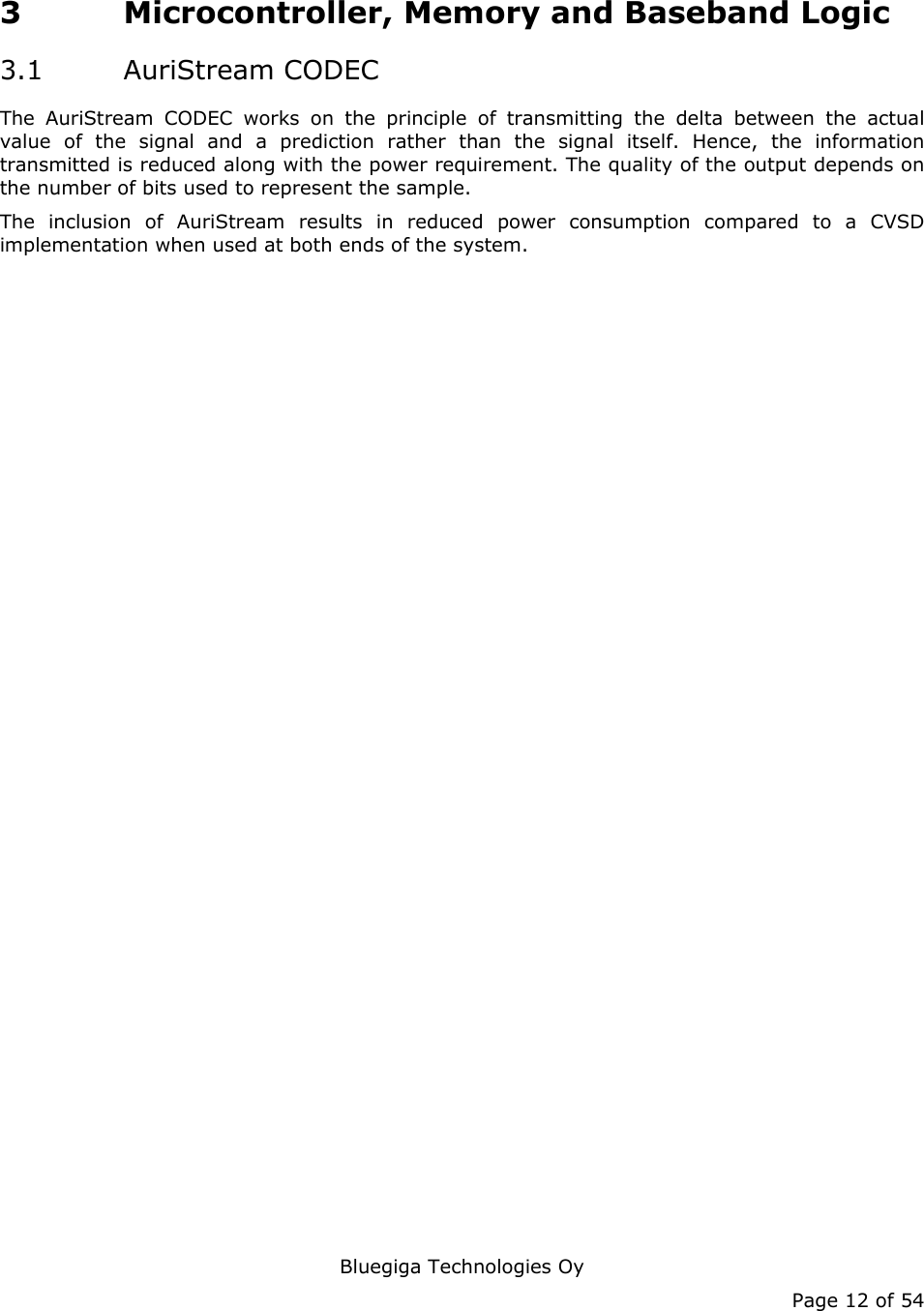
Trapeze Software Group RAN49110 RUGGED AND COMPACT VEHICULAR COMPUTER User Manual WT21 Datasheet
Trapeze Software Group, Inc. RUGGED AND COMPACT VEHICULAR COMPUTER WT21 Datasheet
Contents
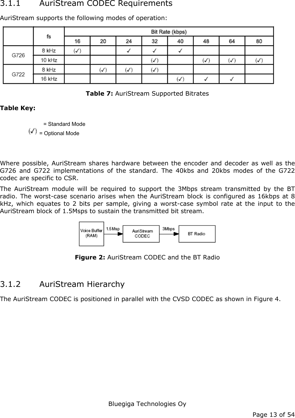
- 1. Users Guide
- 2. Installation Guide
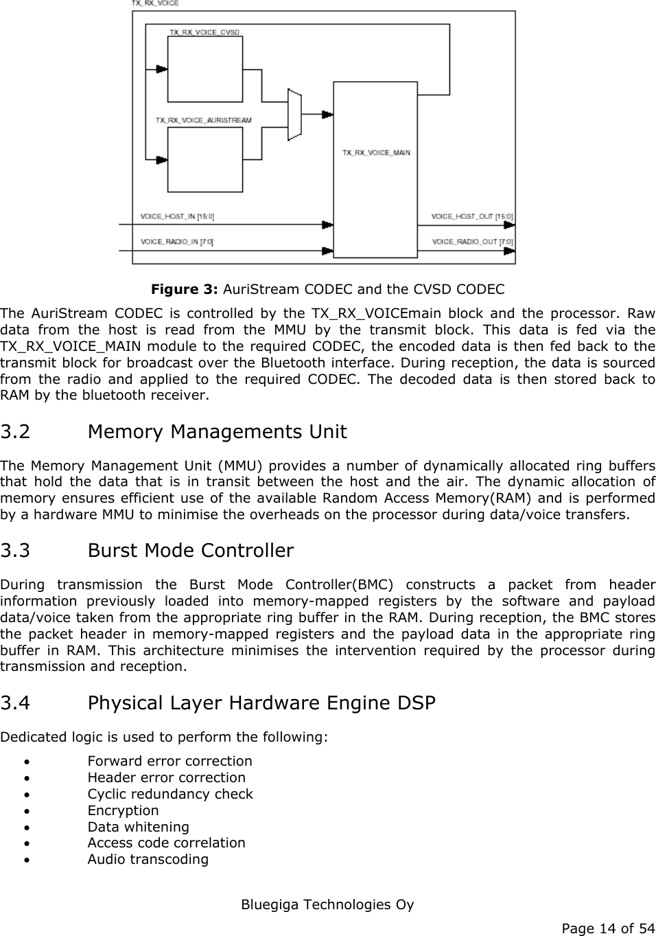
- 3. Users Info
- 4. Install Guide
Users Info
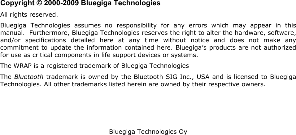
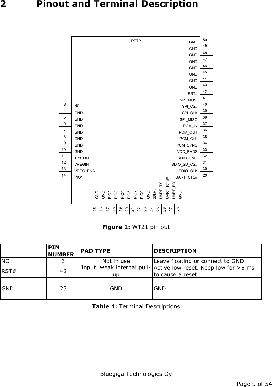
![Bluegiga Technologies Oy Page 10 of 54 POWER SUPPLIES PIN NUMBER DESCRIPTIONVREGIN 12 Input for the internal 1,8V regulator1v8_OUT 11 1,8V regulator outputVREG_ENA 13 Take high to enable internal voltage regulatorsGND 4-10, 15-16, 28, 43-50 GroundVDD_PADS 33 Positive supply for the digital interfaces Table 2: Terminal Descriptions PIO PORT PIN NUMBER PAD TYPE DESCRIPTIONPIO[1] 14 Bi-directional, programmamble strength internal pull-down/pull-upProgrammamble input/output linePIO[2] 17 Bi-directional, programmamble strength internal pull-down/pull-upProgrammamble input/output linePIO[3] 18 Bi-directional, programmamble strength internal pull-down/pull-upProgrammamble input/output linePIO[4] 19 Bi-directional, programmamble strength internal pull-down/pull-upProgrammamble input/output linePIO[5] 20 Bi-directional, programmamble strength internal pull-down/pull-upProgrammamble input/output linePIO[7] 21 Bi-directional, programmamble strength internal pull-down/pull-upProgrammamble input/output linePIO[9] 22 Bi-directional, programmamble strength internal pull-down/pull-upProgrammamble input/output line Table 3: Terminal Descriptions](https://usermanual.wiki/Trapeze-Software-Group/RAN49110.Users-Info/User-Guide-1647794-Page-10.png)
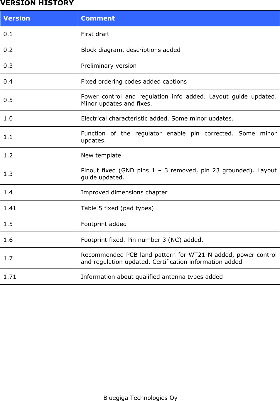
![Bluegiga Technologies Oy Page 11 of 54 SPI INTERFACEPIN NUMBER PAD TYPE DESCRIPTIONPCM_OUT 36 Output, tri-state, weak internal pull-down Synchronous data outputPCM_IN 37 Input, weak internal pull-down Synchronous data inputPCM_SYNC 34 Bi-directional, weak internal pull-down Synchronous data syncPCM_CLK 35 Bi-directional, weak internal pull-down Synchronous data clock Table 4: Terminal Descriptions SDIO/CSPI/UART InterfacesPIN NUMBER PAD TYPE DESCRIPTIONSDIO_DATA[0]Synchronous data input/outputCSPI_MISO CSPI data outputUART_TX UART data output, active highSDIO_DATA[1]Synchronous data input/outputCSPI_INT CSPI data inputUART_RTS# UART request to send, active lowSDIO_DATA[2]Synchronous data input/outputUART_RX UART data input, active highSDIO_DATA[3]Synchronous data input/outputCSPI_CS# Chip select for CSR Serial Peripheral Interface, active lowUART_CTS# UART clear to send, active lowSDIO_CLK SDIO clockCSPI_CLK CSPI clockSDIO_SD_CS# 31Bi-directional, weak internal pull-downSDIO chip select to allow SDIO accessessSDIO_CMD SDIO data inputCSPI_MOSI CSPI data input25Bi-directional, tri-state, weak internal pull-down26Bi-directional, weak internal pull-down27 Bi-directional, weak internal pull-29Bi-directional, weak internal pull-down30 Bi-directional, weak internal pull-32 Bi-directional, weak internal pull- Table 5: Terminal Descriptions SPI INTERFACEPIN NUMBER PAD TYPE DESCRIPTIONSPI_MOSI 41 Weak internal pull-down SPI data inputSPI_CS# 40 Bi-directional, weak internal pull-downChip select for Serial Peripheral Interface, active lowSPI_CLK 39 Bi-directional, weak internal pull-down SPI clockSPI_MISO 38 Output, tri-state, weak internal pull-down SPI data output Table 6: Terminal Descriptions](https://usermanual.wiki/Trapeze-Software-Group/RAN49110.Users-Info/User-Guide-1647794-Page-11.png)
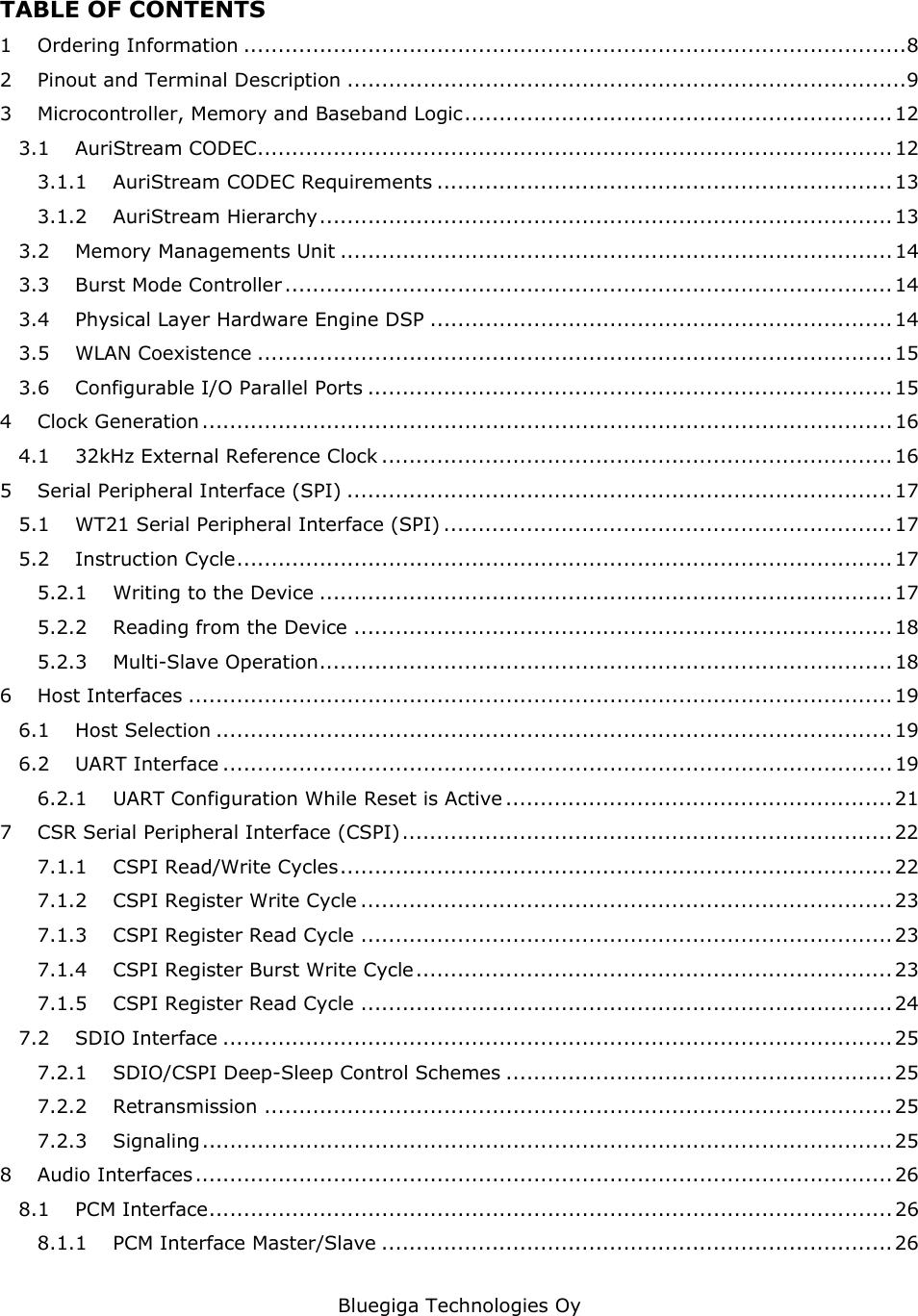
![Bluegiga Technologies Oy Page 15 of 54 The following voice data translations and operations are performed by firmware: • A-law/µ-law/linear voice data (from host) • A-law/µ-law/Continuously variable Slope Delta (CVSD) (over the air) • Voice interpolation for lost packets • Rate mismatches The hardware supports all optional and mandatory features of Bluetooth v2.1 + EDR including AFH and eSCO. 3.5 WLAN Coexistence Dedicated hardware is provided to implement a variety of coexistence schemes. Channel skipping AFH, priority signalling, channel signalling and host passing of channel instructions are all supported. The features are configured in firmware. For more information contact Buegiga technical support. 3.6 Configurable I/O Parallel Ports lines of programmable bi-directional input/outputs (I/O) are provided. PIO[1: 5, 7, 9] are powered from VDD_PADS. PIO lines can be configured through software to have either weak or strong pull-ups or pull-downs. All PIO lines are configured as inputs with weak pull-downs at reset. Any of the PIO lines can be configured as interrupt request lines or as wake-up lines from sleep modes. Bluegiga cannot guarantee that the PIO assignments remain as described. Refer to the relevant software release note for the implementation of these PIO lines, as they are firmware build-specific.](https://usermanual.wiki/Trapeze-Software-Group/RAN49110.Users-Info/User-Guide-1647794-Page-15.png)
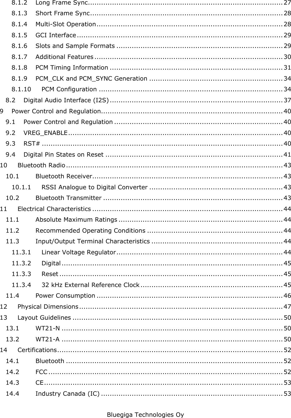
![Bluegiga Technologies Oy Page 16 of 54 4 Clock Generation WT21 uses an internal 26 MHz crystal as a Bluetooth reference clock. All WT21 internal digital clocks are generated using a phase locked loop, which is locked to the 26 MHz reference clock. Also supplied to the digits is a watchdog clock, for use in low power modes. This uses a frequency of 32.768kHz from CLK_32K, or an internally generated reference clock frequency of 1kHz, determined by PSKEY_DEEP_SLEEP_EXTERNAL_CLOCK_SOURCE. The use of the watchdog clock is determined with respect to Bluetooth operation in low power modes. Bluetooth RadioDigitsPLL26 MHz1 kHzCLK_32kHzAIO[0]Watchdog clock Figure 4: Clock Architecture 4.1 32kHz External Reference Clock A 32kHz clock can be applied to CLK_32K, using PSKEY_DEEP_SLEEP_EXTERNAL_CLOCK_SOURCE. The CLK_32K pad is in the VDD_PADS domain with all the other digital I/O pads and is driven between levels specified in Section 11.3.4.](https://usermanual.wiki/Trapeze-Software-Group/RAN49110.Users-Info/User-Guide-1647794-Page-16.png)
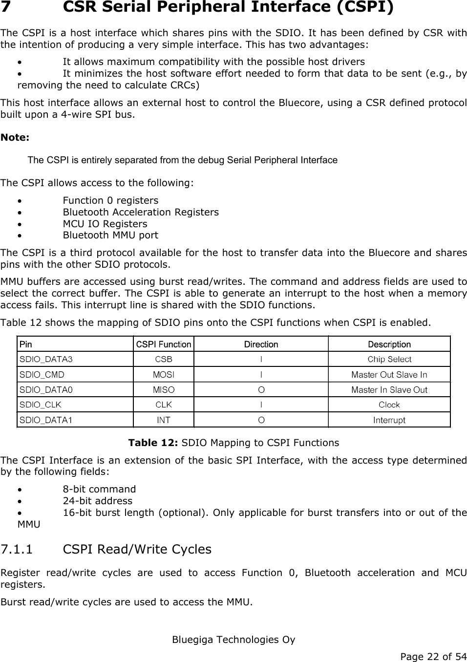
![Bluegiga Technologies Oy Page 17 of 54 5 Serial Peripheral Interface (SPI) 5.1 WT21 Serial Peripheral Interface (SPI) SPI is used for debuging primarily. This section details the considerations required when interfacing to WT21 via the SPI. Data may be written or read one word at a time or the auto increment feature may be used to access blocks. 5.2 Instruction Cycle WT21 is the slave and receives commands on SPI_MOSI and outputs data on SPI_MISO. Table 8 shows the instruction cycle for an SPI transaction. Table 8: Instruction Cycle for an SPI Transaction With the exception of reset, SPI_CS# must be held low during the transaction. Data on SPI_MOSI is clocked into the WT21 on the rising edge of the clock line SPI_CLK. When reading, WT21 replies to the master on SPI_MISO with the data changing on the falling edge of the SPI_CLK. The master provides the clock on SPI_CLK. The transaction is terminated by taking SPI_CS# high. Sending a command word and the address of a register for every time it is to be read or written is a significant overhead, especially when large amounts of data are to be transferred. To overcome this WT21 offers increased data transfer efficiency via an auto increment operation. To invoke auto increment, SPI_CS# is kept low, which auto increments the address, while providing an extra 16 clock cycles for each extra word to be written or read. 5.2.1 Writing to the Device To write to WT21, the 8-bit write command (00000010) is sent first (C[7:0]) followed by a 16-bit address (A[15:0]). The next 16-bits (D[15:0]) clocked in on SPI_MOSI are written to the location set by the address (A). Thereafter for each subsequent 16-bits clocked in, the address (A) is incremented and the data written to consecutive locations until the transaction terminates when SPI_CS# is taken high.](https://usermanual.wiki/Trapeze-Software-Group/RAN49110.Users-Info/User-Guide-1647794-Page-17.png)
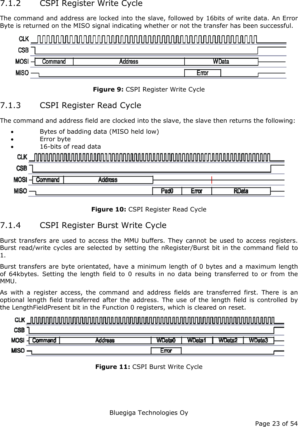
![Bluegiga Technologies Oy Page 18 of 54 Figure 5: SPI Write Operation 5.2.2 Reading from the Device Reading from WT21 is similar to writing to it. An 8-bit read command (00000011) is sent first (C [7:0]), followed by the address of the location to be read (A[15:0]). WT21 then outputs on SPI_MISO a check word during T[15:0] followed by the 16-bit contents of the addressed location during bits D[15:0]. The check word is composed of {command, address [15:8]}. The check word may be used to confirm a read operation to a memory location. This overcomes the problems encountered with typical serial peripheral interface slaves, whereby it is impossible to determine whether the data returned by a read operation is valid data or the result of the slave device not responding. If SPI_CS# is kept low, data from consecutive locations is read out on SPI_MISO for each subsequent 16 clocks, until the transaction terminates when SPI_CS# is taken high. Figure 6: SPI Read Operation 5.2.3 Multi-Slave Operation WT21 should not be connected in a multi-slave arrangement by simple parallel connection of slave MISO lines. When WT21 is deselected (SPI_CS# = 1), the SPI_MISO line does not float. Instead, WT21 outputs 0 if the processor is running or 1 if it is stopped.](https://usermanual.wiki/Trapeze-Software-Group/RAN49110.Users-Info/User-Guide-1647794-Page-18.png)
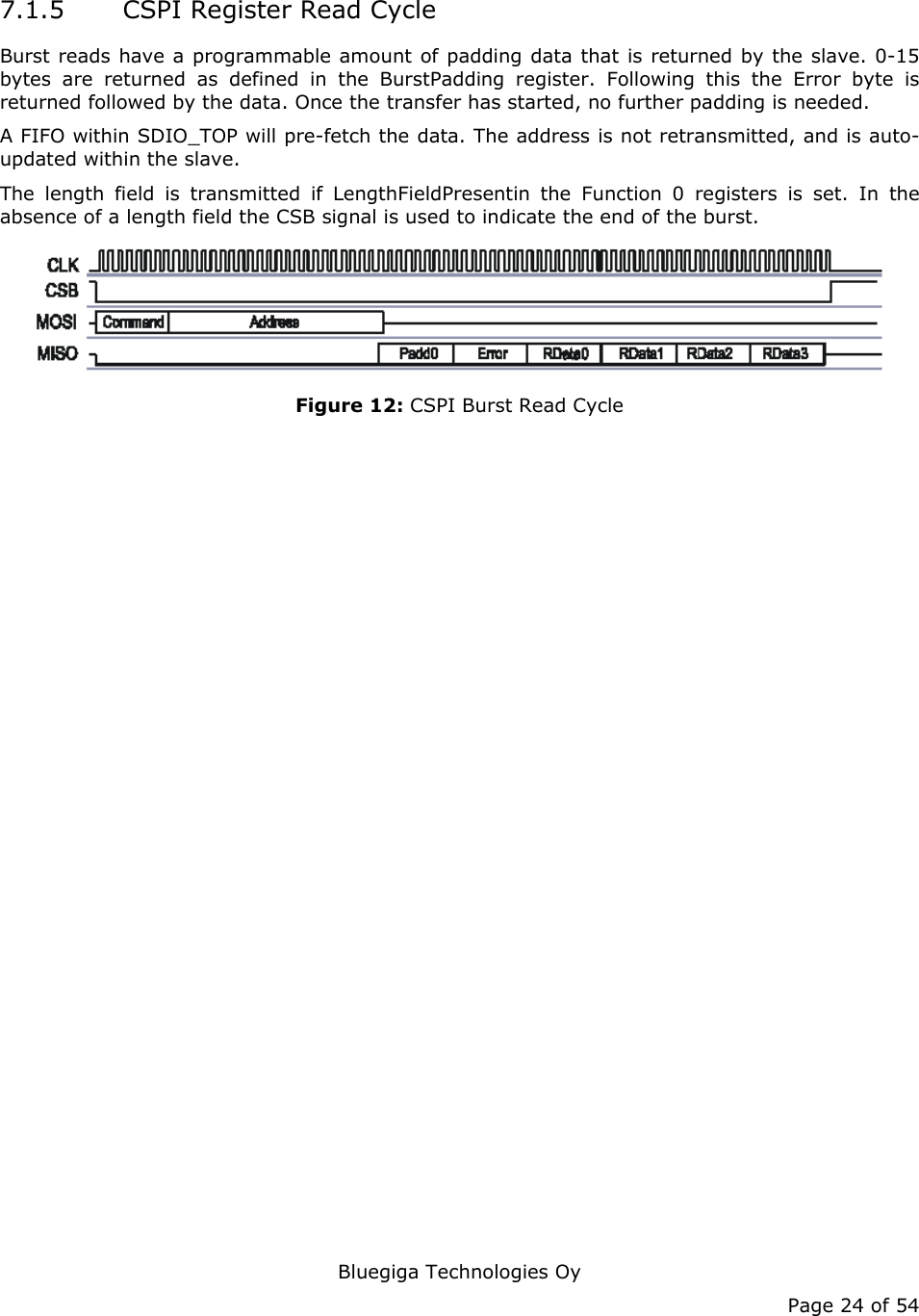
![Bluegiga Technologies Oy Page 19 of 54 6 Host Interfaces 6.1 Host Selection The MCU selects the UART/SDIO interfaces by reading PIO[4] at boot-time. When PIO[4] is high, the SDIO interface is enabled; when PIO[4] is low, the UART is enabled. If in UART mode, the MCU selects the UART transfer protocol automatically using the unused SDIO pins shown in Table 9 SDIO_CLK SDIO_CMD Protocol0 0 bcsp01h41 0 h4ds11h5 Table 9: SDIO_CLK and SDIO_CMD transfer Protocols 6.2 UART Interface This is a standard UART interface for communicating with other serial devices. WT21 UART interface provides a simple mechanism for communicating with other serial devices using the RS232 protocol. Note: WT21 uses RS232 protocol, but voltage levels are 0V to VDD_PADS (requires external RS232 transceiver chip. UART_TXUART_RXUART_RTS#UART_CTS# Figure 7: Universal Asynchronous Receiver Four signals implement the UART function, as shown in Figure 8. When WT21 is connected to another digital device, UART_RX and UART_TX transfer data between the two devices. The remaining two signals, UART_CTS and UART_RTS, can be used to implement RS232 hardware flow control where both are active low indicators.](https://usermanual.wiki/Trapeze-Software-Group/RAN49110.Users-Info/User-Guide-1647794-Page-19.png)
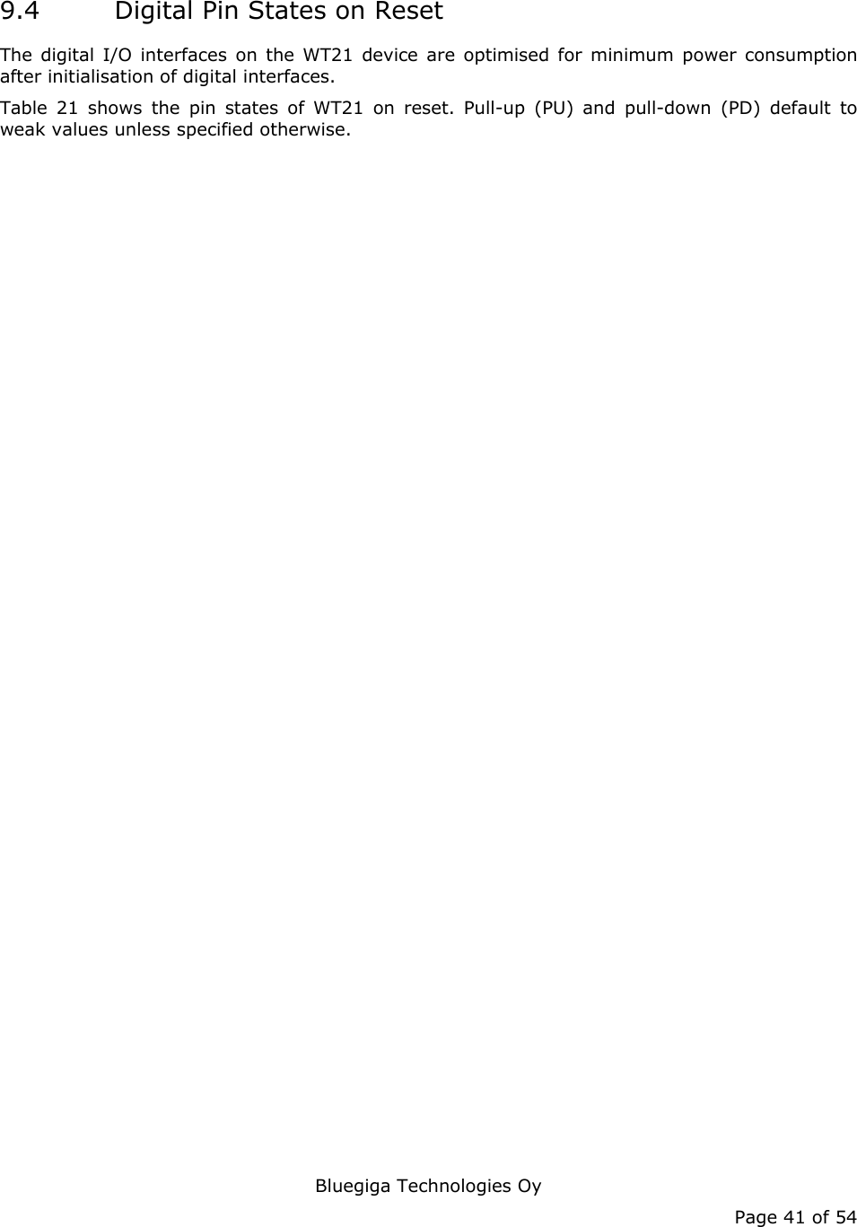
![Bluegiga Technologies Oy Page 42 of 54 Pull R I/O Pull R I/ORST# Digital Input PU Input PU InputPull R I/O Pull R I/OSDIO_DATA[3] Digital bi-directional PD Input PU InputSDIO_DATA[2] Digital bi-directional PD Input PU InputSDIO_DATA[1] Digital bi-directional PD Input PU InputSDIO_DATA[0] Digital bi-directional PD Input PU InputSDIO_SD_CS# Digital bi-directional PD Input PU InputSDIO_CMD Digital bi-directional PD Input PU InputSDIO_CLK Digital bi-directional PD Input PU InputPull R I/O Pull R I/OPCM_IN Digital Input PD Input PD InputPCM_OUT Digital tri-state output PD High impedance PD High impedancePCM_CLK Digital bidirectional PD Input PD InputPCM_SYNC Digital bidirectional PD Input PD InputPull R I/O Pull R I/OSPI_MOSI Digital input PD Input PD InputSPI_CLK Digital input PD Input PD InputSPI_CS# Digital input PU PU PU InputSPI_MISO Digital tri-state output PD PD PD High impedancePull R I/O Pull R I/OPIO[0] Digital bi-directional PD Input PD InputPIO[1] Digital bi-directional PD Input PD InputPIO[2] Digital bi-directional PD Input PD InputPIO[3] Digital bi-directional PD Input PD InputPIO[4] Digital bi-directional PD Input PD InputPIO[5] Digital bi-directional PD Input PD InputPIO[7] Digital bi-directional PD Input PD InputPIO[9] Digital bi-directional PD Input PD InputPull R I/O Pull R I/OCLK_32K Digital input PD Input PD InputPIOsSPI InterfacePin Name / Group I/O Type No Core Voltage Reset Full Chip ResetPin Name / Group I/O Type No Core Voltage Reset Full Chip ResetPin Name / Group I/O Type No Core Voltage Reset Full Chip ResetReset / ControlPin Name / Group I/O Type Full Chip ResetPCM InterfaceDigital Interfaces - SDIONo Core Voltage ResetPin Name / Group I/O Type No Core Voltage Reset Full Chip ResetClockPin Name / Group I/O Type No Core Voltage Reset Full Chip Reset Table 21: Pin States of WT21 on Reset](https://usermanual.wiki/Trapeze-Software-Group/RAN49110.Users-Info/User-Guide-1647794-Page-42.png)