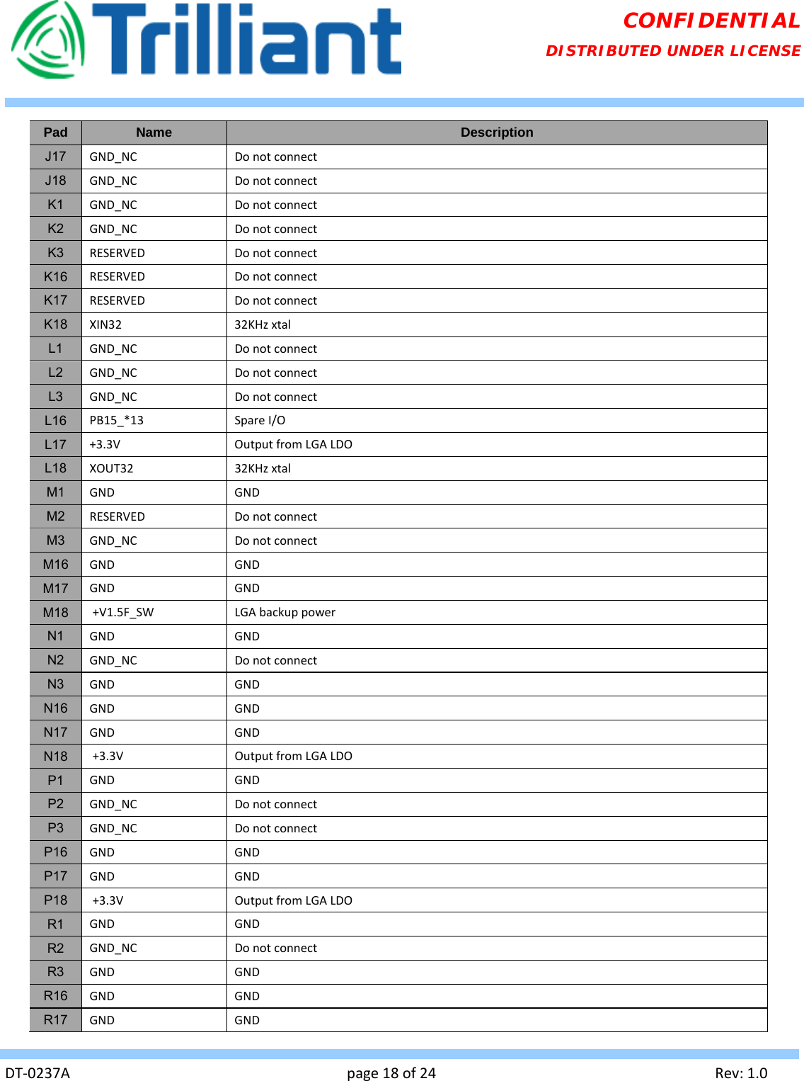
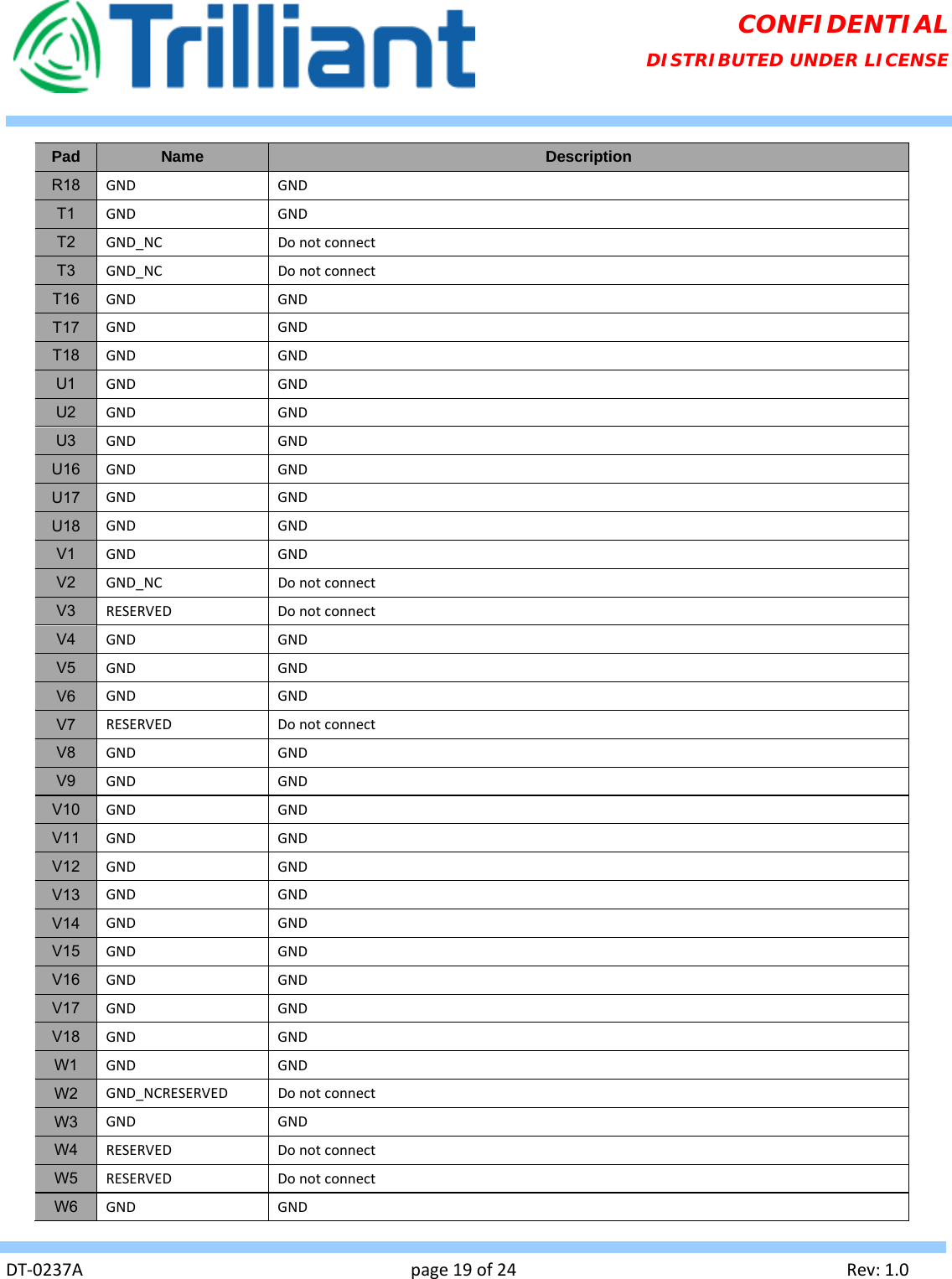
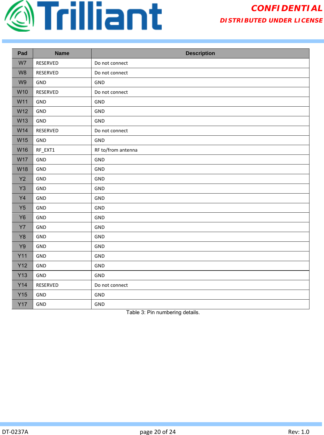
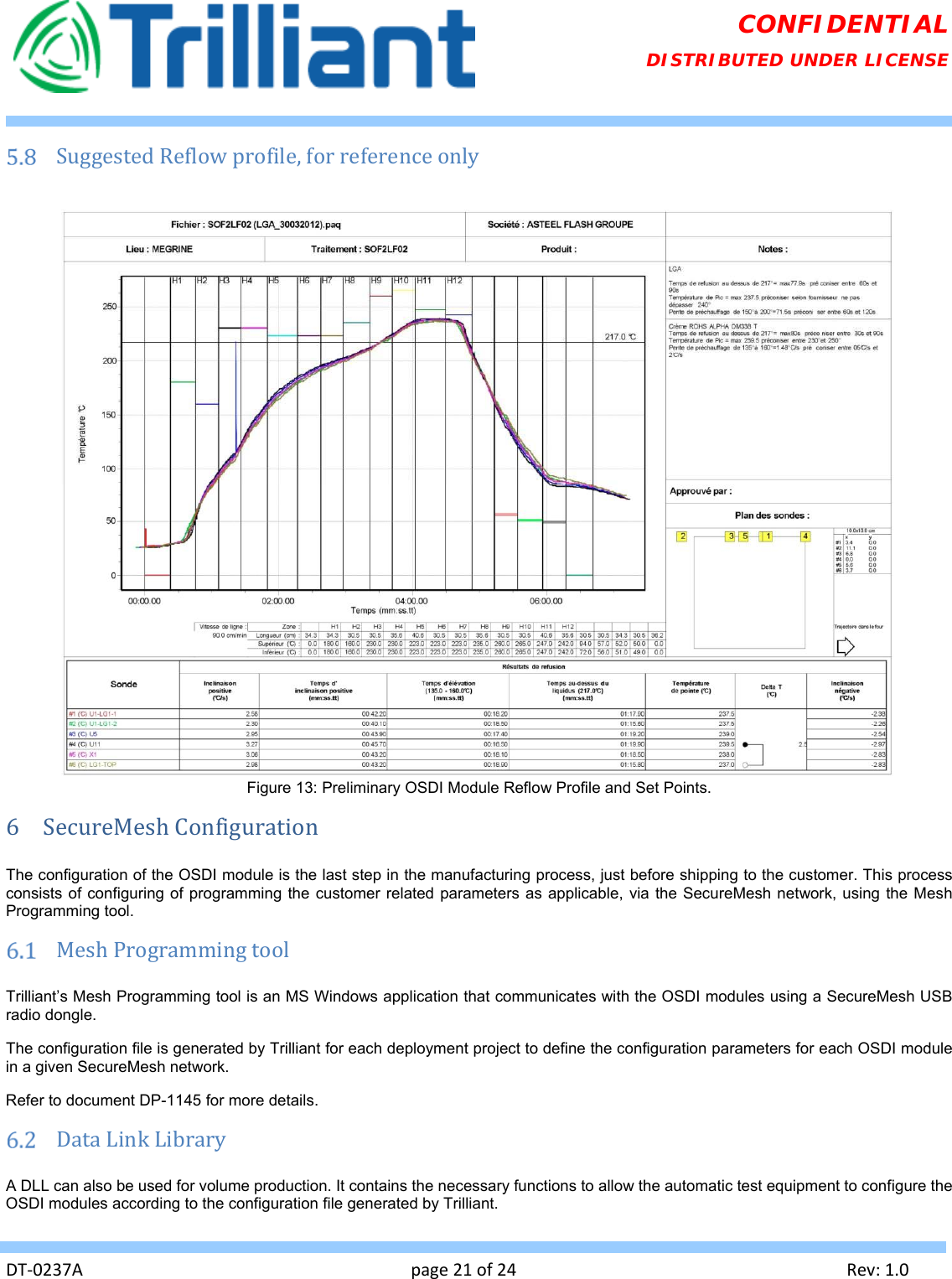
Trilliant Networks OSDI4W1 IEEE 802.15.4 Transceiver Module User Manual

Trilliant Networks IEEE 802.15.4 Transceiver Module

Contents

User Manual

  DT‐0237Apage1of24Rev:1.0CONFIDENTIAL DISTRIBUTED UNDER LICENSE  Hardware User Guide Overview for Open Smart Device Interface (OSDI) SecureMesh™ Module    Models:   OSDI-4000-1D  OSDI-4000-1A PRINTEDVERSIONSOFTHISDOCUMENTAREUNCONTROLLEDDistributedunderlegalcommercialagreementDOCUMENT RELEASE/APPROVALS  document #  DT-0237A current revision  1.0 approvals name  title date         
  DT‐0237Apage2of24Rev:1.0CONFIDENTIAL DISTRIBUTED UNDER LICENSE  LEGAL NOTICES  THIS DOCUMENT CONTAINS SENSITIVE PROPRIETARY AND CONFIDENTIAL INFORMATION OWNED BY TRILLIANT NETWORKS.  THIS DOCUMENT HAS BEEN PROVIDED TO YOUR COMPANY THROUGH A PREVIOUSLY EXECUTED OSDI MODULE DESIGN LICENSE AGREEMENT AND MAY NOT BE DISTRIBUTED TO ANY OTHER 3RD PARTY, IN ANY FORM OR PORTION, WITHOUT TRILLIANT’S EXPRESSED WRITTEN PERMISSION.  LICENSEE ACKNOWLEDGES THAT  THE OSDI MODULE DOCUMENTATION PACKAGE AND TOOLS ARE LICENSED TO IT ON  AN "AS IS" BASIS.  TRILLIANT MAKES NO OTHER REPRESENTATIONS AND EXTENDS NO OTHER WARRANTIES OR CONDITIONS OF ANY KIND,  EXPRESS, IMPLIED OR STATUTORY INCLUDING WARRANTIES OF  NONINFRINGEMENT, MERCHANTABILITY AND FITNESS FOR A PARTICULAR USE.  EXCEPT AS OTHERWISE EXPRESSLY SET FORTH IN THIS LICENSE, TRILLIANT ASSUMES NO RESPONSIBILITIES OR  LIABILITIES WHATSOEVER WITH RESPECT TO USE OR SALE BY EITHER LICENSEE OR ITS VENDEES OR TRANSFEREES OF COMBINED PRODUCTS.   THE INFORMATION CONTAINED IN THIS DOCUMENT IS SUBJECT TO CHANGE WITHOUT NOTICE. TRILLIANT RESERVES THE RIGHT TO CHANGE THE PRODUCT SPECIFICATIONS WITHOUT CONSEQUENCE OF LIABILITY.                   Trilliant Incorporated 1100 Island Drive, Redwood City, CA 94065 USA +1.650.204.5050 www.trilliantinc.com Trilliant™, CellReader®, CellGateway™, SecureMesh™, SerViewCom®, UnitySuite™, SkyPilot®, SyncMesh™, the Trilliant logo, and the SkyPilot logo are trademarks of Trilliant Incorporated and/or its subsidiaries.  All other trademarks are the property of their respective owners.   Copyright © 2015 Trilliant Incorporated.  ALL RIGHTS RESERVED.
  DT‐0237Apage3of24Rev:1.0CONFIDENTIAL DISTRIBUTED UNDER LICENSE TableofContents1Overview..................................................................42FeaturesandSpecifications.......................................4SecureMeshNANRadioPerformance..................4Electricalspecifications.........................................4Physical,&Environmental....................................5Compliance...........................................................53FunctionalDescription..............................................6OSDIModule.........................................................6HostInterface&OptionalIOs...............................6InterfaceandControlSignals...............................64Antennas..................................................................8AntennaPlacement..............................................8Externalantennas.................................................95HostPCBRequirements...........................................11RecommendedFootprint....................................11PasteMask..........................................................11Layoutrequirements..........................................11Referencetracedesign.......................................12ModifyingtheRFSignalRouting........................13PinNumbering....................................................15PinDescription....................................................15SuggestedReflowprofile,forreferenceonly......216SecureMeshConfiguration.......................................21MeshProgrammingtool....................................21DataLinkLibrary................................................217RegulatoryAgencyApprovals..................................22UnitedStates......................................................22Canada...............................................................23 FiguresFigure1:TypicalapplicationwithOSDIModule.............................................................................................................................6Figure2:LarsenRO2406NMDrawing.............................................................................................................................................9Figure3:LarsenRO2406NMRadiationPatterns.............................................................................................................................9Figure4:MobileMarkCVS‐2400..................................................................................................................................................10Figure5:MobileMarkCVS‐2400RadiationPatterns....................................................................................................................10Figure6FootprintOSDI‐4000‐1X..................................................................................................................................................11Figure7FCCandICapprovedtracedesignlayoutandpicture.....................................................................................................12Figure8Couponrequirementstovalidatetraceimpedance........................................................................................................13Figure9:Micro‐striptraceparameters.........................................................................................................................................14Figure10:Examplestack‐up........................................................................................................................................................14Figure11:50ohmscalculation(mm)Tracewidth:0.7mmCopperclearance:0.1445mm..............................................................14Figure12:PinNumberingDiagramBottomview..........................................................................................................................15Figure13:PreliminaryOSDIModuleReflowProfileandSetPoints...............................................................................................21TablesTable1:OSDImodulecontrolsignalsdescriptionandusage..........................................................................................................6Table2Antennamicro‐striptraceparts......................................................................................................................................13Table3:Pinnumberingdetails.....................................................................................................................................................20
  DT‐0237Apage4of24Rev:1.0CONFIDENTIAL DISTRIBUTED UNDER LICENSE 1 OverviewThe SecureMesh Ready, Open Smart Device Interface Modules (OSDI) are Trilliant 2.4GHz RF modules which can be integrated into a variety of third party OEM products. These small and versatile modules include a microcontroller, memory, transceiver, power management all on an LGA circuit board.  Based on IEEE 802.15.4 wireless communication standard and utilizing Trilliant’s robust SecureMesh networking protocol, the OSDI modules deliver industry leading 2.4GHz networking solution. The modules are easy to integrate, provide low power consumption, long range and many more features and functionalities. The OSDI family of products are currently available in 2 base hardware models:  Hardware Model  Description OSDI-4000-1A 4th generation OSDI module with maximum transmit power of 1 watt; ANSI protocol OSDI-4000-1D 4th generation OSDI module with maximum transmit power of 1 watt; DLMS/COSEM Protocol  Throughout the remainder of this document, the OSDI module platforms will be referred to by the base hardware model. 2 FeaturesandSpecificationsThe OSDI modules are designed for a broad range of applications and products, and provide a compliant ready RF mesh solution for both domestic and international markets. The modules have a unique set of features, including:   Reporting Retries and Acknowledgements.   Remote Firmware upgrades.   Programmable Network Parameters.   AES, DES Encryption crypto module.   Frequency hopping for a reliable communication link against interference (future enhancement)  SecureMeshNANRadioPerformanceProtocols   SecureMesh NAN Transport layer   SecureMesh NAN Network layer   IEEE 802.15.4 MAC layer    IEEE 802.15.4 PHY layer (2.4 GHz) Modulations DSSS – OQPSK  Direct Sequence Spread Spectrum Offset Quadrature Phase-Shift Keying Data rate: 250 kbps (transmit/receive) Frequency band  2.400 - 2.4835 GHz (unlicensed operation) Frequency channels  15 Channel spacing  5 MHz Maximum transmit power  +30dBm Receive sensitivity  -103dBm    Electricalspecifications Min.  Typ.  Max. Voltage 4.0  4.5  5.0 Current   1. 2A
  DT‐0237Apage5of24Rev:1.0CONFIDENTIAL DISTRIBUTED UNDER LICENSE   Physical,&EnvironmentalMounting method  LGA (Land Grid Array)  Dimensions (L x W x H)  29.8 x 35.3 x 4.4 mm Operating temperature   -40 °C to +85 °C  Humidity  5 to 95% non-condensing    ComplianceRadio emissions   FCC Part 15 Class B   Industry Canada ICES-003 Class B  MID   others pending Unlicensed radio operation   FCC Part 15.212, 15.247   Industry Canada RSS-Gen, RSS-247  MID  others pending Human Exposure   FCC Part 1.1310  RSS-102  
  DT‐0237Apage6of24Rev:1.0CONFIDENTIAL DISTRIBUTED UNDER LICENSE 3 FunctionalDescription OSDIModuleThe OSDI modules are low power 2.4GHz ISM band transceivers. Figure 1 below shows a block diagram of the OSDI-4000 modules and the surrounding optional functionalities that are intended as a reference implementation example.  The configuration of the transceiver, reading and writing of Frame Buffer is controlled by a SPI interface and additional control lines. The control of the RF front-end is done via the transceiver digital control pins. The OSDI modules are equipped with a Low Drop Out voltage (LDO) regulator that enables them to work in standalone mode with a voltage supply between 4 and 5 volts.  The VCPU power supply line of the microcontroller is available on the external connection for optional backup supply when Real Time Power Outage Reporting (RTPOR) is required.  Figure 1: Typical application with OSDI Module  HostInterface&OptionalIOsCommunication with the host is achieved using a serial communication port and control signals that are bundled with the power lines inside the host connector. Diagnostic and programming signals are available to the host.  See Table 1 below for the description of the various signals found in the diagnostic and programming interface.  The RF input/output signal must be routed through the host device as described in section 5.4.  Antennas of section 4 can be used in relation with regulation.   The OSDI module is designed with outputs to drive a multicolor LED indicator that allows visual diagnostic and status monitoring of the device. See Table 1 below for an interpretation of the existing LED patterns.  InterfaceandControlSignalsTable 1: OSDI module control signals description and usage. Signal  Description  Usage TX_EXT-RX_LGA  Transmit from the meter / Receive to the module.  Signal Type: UART.   Meter Connector serial port.   Meter USB Port.   Default baud rate is set to 9.6 kbps. RX_EXT-TX_LGA  Receive to the meter / Transmit from the module.  Signal Type: UART.
  DT‐0237Apage7of24Rev:1.0CONFIDENTIAL DISTRIBUTED UNDER LICENSE Signal  Description  Usage DIAG-RX_LGA  Module receive diagnostic port.  Signal Type: UART.   Diagnostic serial port   Diagnostic USB Port.   Default baud rate is set to 9.6 kbps in diagnostic mode and 19.2 kbps in trace mode.   Should be accessible via test points in normal design. DIAG-TX_LGA Module transmit diagnostic port.  Signal Type: UART. RED_LED and GRN_LED Control Red and Green LEDs. Signal Type: Active low output. 0=LED on, 1= LED off. Note: Red and green led are in one physical unit. Yellow is produced when both LEDs are on.  Diagnostic LEDs.   Needs to be visible from the outside of the meter for installation purposes in normal design. LEDs off: Power save mode/POR mode or no power. Flashing green: Initialization (5 sec). Steady Red: Working but not associated to a network. Steady Yellow: Working and trying to associate to a network. Steady Green: Working and associated to a network. Flashing Yellow: Working and exchanging info. P-FAIL_EXT   External signal from the meter indicating that an interruption of power has been detected. Signal Type: Active low input from the meter. 0 = Power fail, 1 = Normal condition.  Meter Connector.  PFAIL Circuit. Provides an early detection of power outage events. P-FAIL   Signal indicating that an interruption of power has been detected. Signal Type: Interrupt input. 0 = Power fail, 1 = Normal condition.  PFAIL Circuit.   CPU Reset Control Circuit. Provides early detection of power outage events. RESET  Signal Type: Hardware reset. 0 = Reset, 1 = Normal operation.   CPU Reset Control Circuit.   For use during development only.   Do not connect to the meter. TEST  Select test / diagnostic mode. Signal Type: Active high input. 1 = Diagnostic mode, 0 = Normal mode.  Reserved  Diagnostic/Programming Connector.   Should be accessible via test points in normal design. SC_HI  Signal Type: Input. 1 = Supercap voltage > 3.6V   On/off signal from the fail safe circuit to detect if the super cap is higher than 3.6V. PWR_MON  Power supply monitoring signal. Signal Type: Analog.  Meter Connector. Provision for self-detection of power outages by the OSDI modules, if P-FAIL is not available. RESET-PDI_CLK,  TDI-PDI_DATA, TDO, TMS, TCK Program and Debug Interface.  Diagnostic/Programming Connector.   Used only during development.   See schematic for proper use.    Should be accessible via test points in normal design. SLEEP  Sleep mode power activation. Signal Type: low open-drain output. 0 = SLEEP Enabled, 1 = SLEEP Disabled.   RTPOR Supply Management circuit. Used to send the command to the power management circuit to connect the 1.5 Farad capacitor (+V1.5F) directly to the input supply (+VCPU) of OSDI module’s CPU in order to feed it with minimum power waste, in sleep mode. MESURE_VCAP  1.5 Farad capacitor voltage monitoring. Signal Type: Analog, feeds ADC input. Provision for monitoring of voltage level of the 1.5F capacitor. +3.3V  LDO voltage regulator’s output.  Regulated 3.3V voltage supply from the OSDI module. +VMAIN  Main power supply input.  Used by the power management circuit as input to the LDO regulator and to charge the 1.5 Farad super capacitor. +VCPU2  3.3 Volts supply for OSDI module’s CPU.  Used to feed power to the CPU during debug and programming. +VCPU  3.3 Volts supply for OSDI module’s CPU.  Input supply (+VCPU) of OSDI module’s CPU. +VLDO_IN  LDO regulator’s input.  Input of the LDO regulator (+VLDO) of the OSDI module. +V1.5F_SW  1.5 Farad capacitor switched voltage.  Power path for the sleep mode power supply.
  DT‐0237Apage8of24Rev:1.0CONFIDENTIAL DISTRIBUTED UNDER LICENSE 4 AntennasThe maximum output power authorized by the FCC and industry Canada in the 2.4GHz band is 36 dBm EIRP. For the OSDI-4000-1X, the maximum output power of the radio is 30 dBm which can be combined to an antenna with a maximum gain of 6 dBi. The OSDI module has been certified with two different types of integrated antennas as described in the following sections. The information shown was taken from datasheets or measured when mounted on specific products. Actual patterns will be influenced by the PCB layout and by surrounding material.  NOTE: Certification regulations differ from one country to the other. It remains the responsibility of the meter manufacturer to choose an antenna that will meet the requirements of the country where the meters will be deployed as well as any local certifications that may be required to comply with specific market regulations. See section 7 for more details.  AntennaPlacementAntenna performance is significantly impacted by the type and physical placement of the antenna.  The antenna should be oriented in the device to properly radiate the RF emissions from the face of the device forward and in an upward direction for optimal connectivity to the Trilliant SecureMesh network infrastructure. In addition, there should be as few obstacles as possible between the antenna and the outside of the device. Through the following examples, Trilliant is attempting to provide antenna options for the most commonly used antenna design scenarios but keep in mind that this is greatly dependent on the host device design. If you are unsure about which antenna to select, or how it should be implemented into the overall design, please contact Trilliant for guidance. The RF connection from the OSDI module to the antenna is made using a 50 ohms micro-strip trace on the host’s PCB. See section 5.4 for routing instructions.
  DT‐0237Apage9of24Rev:1.0CONFIDENTIAL DISTRIBUTED UNDER LICENSE  ExternalantennasThe following section describes types of external antennas that have been certified with the OSDI-4000 module. Note that a Reverse Polarity connector must be used for external antennas.4.2.1 LarsenRO2406NMVendor: Larsen  Vendor #: RO2406NM Frequency: 2400-2500 MHz Nominal Impedance: 50 Ohms VSWR: 2:1 Max Gain: 6 dBi Polarization: Vertical Power withstanding: 20 W Connector: N-Type Male (To use this antenna with the OSDI module, a RP connector that is actually in discussion, must be used; the part number will change accordingly)   Figure 2: Larsen RO2406NM Drawing.  Figure 3: Larsen RO2406NM Radiation Patterns.
  DT‐0237Apage10of24Rev:1.0CONFIDENTIAL DISTRIBUTED UNDER LICENSE 4.2.2 MobileMarkCVS‐2400 Vendor = Mobile Mark Vendor #: CVS-2400-2SA-BLK-13 Frequency: 2.4 – 2.5 GHz Gain: 2.0 dBi max VSWR: 2:1 over band Impedance: 50 ohm nominal Maximum Power: 10 Watts Connector: SMA Plug-RP Temperature Range: -40° to +85°C   Antenna Dimensions:  3 3/4" Length x 1 1/4" Width x 3/8” Deep (95 mm x 32 mm x 9 mm)     Figure4:MobileMarkCVS‐2400.       Figure 5: Mobile Mark CVS-2400 Radiation Patterns.
  DT‐0237Apage11of24Rev:1.0CONFIDENTIAL DISTRIBUTED UNDER LICENSE 5 HostPCBRequirements RecommendedFootprintThe footprints shown below are available upon request as a PAD Layout source file. OSDI-4000-1X      Overall (L x W x H), including shield: 29.8 x 35.3 x 4.0mm   Suggested Silkscreen Outline (L x W): 30.3 x 35.8mm   Avoid vias, traces or copper inside Keep-Out Areas Figure 6 Footprint OSDI-4000-1X  PasteMaskPaste Mask Stencil openings can be of the same size as the recommended footprint (1:1); suggested thickness of stencil foil ≥ 120µm.  Layoutrequirements  Traces routed to RF_EXT pad must be 50 ohm.   Traces current rating:  +VCPU  ≥ 90 mA +3.3V  ≥ 90 mA +VLDO_IN  ≥ 1.4 Amp +V1.5F_SW  ≥ 90mA   Thermal reliefs are strongly recommended for all pads connected to Ground net.   Finish recommendation for PCB pad surfaces: ROHS Compliant (EU Directive 2002/95/EC) 2-10 µIN Immersion Gold Over 50-200µIN Electro less Nickel (ENIG)   Non Solder Mask Defined (NSMD) type is recommended for the solder pads on the PCB.
  DT‐0237Apage12of24Rev:1.0CONFIDENTIAL DISTRIBUTED UNDER LICENSE    Pads Solder Mask Opening of 0.1mm is recommended.   Referencetracedesign5.4.1 LayoutandpartsRF traces from OSDI module pads W10 and W16 to the antenna must be made using micro-strip traces.  This micro-strip trace must respect the design of the Gerber file associated with the following figures in order to obtain a uniform transmission line with a characteristic impedance of 50 ohms.  The reference trace design is shown as the green trace along with the side copper filled with vias on the left side of Figure 7 where components G8, G10, G15, G16 and G18 are not installed; they were options on the reference board for future uses; these uses are not FCC authorized yet.  As preliminary information the traces width of all sections are all 0.27mm and the length of each section, starting from the LGA pad to J53 connector are: LGA pad to G7: 15.38mm; G7 to G9: 12.37mm; G9 to G17: 6.7mm; G17 to R52: 2.1mm; R52 to J53: 7.2mm.  However, refer to associated Gerber files for more accurate details on dimensions and refer to Trilliant Networks Inc for more details on the Gerber files.  Table 2 shows the parts used in the reference trace design.     Figure 7  FCC and IC approved trace design layout and picture
  DT‐0237Apage13of24Rev:1.0CONFIDENTIAL DISTRIBUTED UNDER LICENSE Table 2  Antenna micro-strip trace parts Part Number  Designator  Description  Manufacturer N/A  G8, G10, G15, G16, G18  Not installed  N/A RK73Z1ETTP  G7, G9, G17, R52  RESISTOR 0.0 OHMS 1/16W 5% 0402 SMT KOA Speer Electronics LQW18AN75NG00D  L2  INDUCTOR 75nH, 2%, 270mA 560mΩ, 0603 SMT Murata Manufacturing 1-1478979-0  J53  SMA JACK CONNECTOR (FEMALE) PCB Mount 4 legs, SS/Gold pl. TE Connectivity 5.4.2 Designvalidation&productionproceduresTo verify compliance of the reference trace, a coupon must be requested with every manufacturing panel form and for which the characteristics are described in the Gerber files.  Part of these characteristic are shown in Figure 8.  Then a network analyzer is used to measure the impedance of this coupon in order to validate the antenna trace.  Figure 8  Coupon requirements to validate trace impedance 5.4.3 OtherconsiderationsThe only antennas, also describe is section 4.2, that can be used with the module using the reference trace design are the: - Larsen Antennas, RO2406NM, 6 dBi  - Mobile Mark, CVS-2400, 2.5 dBi The use of any other antenna or any changes to the reference trace design are subject to additional testing and authorization through a Class II permissive change.  ModifyingtheRFSignalRoutingAs previously mentioned, any changes to the RF traces is subject to approbation, additional testing and authorization through a Class II permissive change on the FCC and IC grants. The objective is to use the W10 and W16 pads from OSDI module to route a micro-strip traces in order to obtain a uniform transmission line with a characteristic impedance of 50 ohms.  The characteristic impedance depends on the geometry of the trace and on the relative dielectric constant of the PCB as shown in Figure 9. However, the characteristic impedance does not depend on the length of the trace. Many tools are available on the web to help calculate the optimum dimensions.
  DT‐0237Apage14of24Rev:1.0CONFIDENTIAL DISTRIBUTED UNDER LICENSE  Figure 9: Micro-strip trace parameters H1 and T1 are taken from the stack-up parameter of the host’s PCB as shown in Figure 10, the relative dielectric constant depend on the material used.  Figure 10: Example stack-up An example stack-up, copper thickness, RF traces width and traces to copper clearance in order to get 50 ohms is presented below. The calculation toll is then used to find the remaining parameters of the micro-strip traces as shown in Figure 11.  Figure 11: 50 ohms calculation (mm) Trace width: 0.7mm Copper clearance: 0.1445mm The resulting parameters can then be used to define the trace width and copper clearance on RF traces of the host’s PCB. The RF traces must be surrounded by copper all along the path of undefined length; the path should be as short as possible to reduce losses. Vias must be added all along the RF traces.  See reference trace design in Figure 7 for an example. Note: a new trace design is subject to validation, additional testing and authorization through a Class II Permissive change on the FCC and IC grants.
  DT‐0237Apage15of24Rev:1.0CONFIDENTIAL DISTRIBUTED UNDER LICENSE  PinNumbering Figure 12: Pin Numbering Diagram Bottom view  PinDescriptionPad  Name  Description A2  *8_NRSTTestpointonlyA3  PB31DonotconnectA4  PB23/AD4SpareI/OA5  PA12/AD0SpareI/OA6  RESERVEDDonotconnectA7  +VCPU+VCPUA8  *12_PA16SpareI/OA9  PB28SpareI/OA10  PB4/RX0TestpointonlyA11  PB5/TX0TestpointonlyA12  PB7StatusLEDA13  RESERVEDDonotconnect
  DT‐0237Apage16of24Rev:1.0CONFIDENTIAL DISTRIBUTED UNDER LICENSE Pad  Name  Description A14  +VCPU+VCPUA15  RESERVEDDonotconnectA16  PA0_*1SpareI/OA17  *1_PB26SpareI/OB1  PA13/SCK_EXT1ProvisionforexternalSPIB2  PA14/CS_EXT1ProvisionforexternalSPIB3  PA15SpareI/OB4  PB27PowermanagementsignalB5  RESERVEDDonotconnectB6  RESERVEDDonotconnectB7  RESERVEDDonotconnectB8  RESERVEDDonotconnectB9  PA2_*5SpareI/OB10  RESERVEDDonotconnectB11  SHDNPowermanagementsignalB12  PB8StatusLEDB13  PB25SpareI/OB14  PB10_*4SpareI/OB15  PB14_*5SpareI/OB16  PB11_*6SpareI/OB17  PB12_*1SpareI/OB18  PB16/MISO_EXT2_*2SpareI/OC1  PA10/MOSI_EXT1ProvisionforexternalSPIC2  PB1/TDO_*11SpareI/OC3  RESERVEDDonotconnectC4  PA17/PFAILPowermanagementsignalC5  RESERVED DonotconnectC6  RESERVEDDonotconnectC7  RESERVEDDonotconnectC8  RESERVEDDonotconnectC9  RESERVEDDonotconnectC10  RESERVEDDonotconnectC11  +VCPU+VCPUC12  GND_NCDonotconnectC13  PB29SpareI/OC14  RESERVEDDonotconnectC15  PC0/TX1Meterinterface
  DT‐0237Apage17of24Rev:1.0CONFIDENTIAL DISTRIBUTED UNDER LICENSE Pad  Name  Description C16  RESERVEDDonotconnectC17  RESERVEDDonotconnectC18  RESERVEDDonotconnectD1  PA9/MISO_EXT1ProvisionforexternalSPID2  PB3/TCK_*11SpareI/OD3  PB2/TMS_*11SpareI/OD16  GND_NCDonotconnectD17  RESERVEDDonotconnectD18  PC1/RX1MeterinterfaceE1  *9_NRSTTestpointonlyE2  RESERVEDDonotconnectE3  PB13/AD3PowermanagementsignalE16  PA19/CS_EXT2_*2SpareI/OE17  PB18/SCK_EXT2_*2SpareI/OE18  PB17/MOSI_EXT2_*2SpareI/OF1  PB0/TDISpareI/OF2  PA4/AD1PowermanagementsignalF3  RESERVEDDonotconnectF16  RESERVEDDonotconnectF17  RESERVEDDonotconnectF18  +VLDO_INInputofLGALDOG1  RESERVEDDonotconnectG2  *3_PC5SpareI/OG3  +VCPU+VCPUG16  GND_NCDonotconnectG17  GND_NCDonotconnectG18  +VLDO_INInputofLGALDOH1  RESERVEDDonotconnectH2  GND_NCDonotconnectH3  RESERVEDConnectedtoGndvia0ohmsresistor.H16  GND_NCDonotconnectH17  GND_NCDonotconnectH18  GND_NCDonotconnectJ1  GND_NCDonotconnectJ2  GND_NCDonotconnectJ3  RESERVEDConnectedtoGndvia0ohmsresistor.J16  GND_NCDonotconnect
  DT‐0237Apage18of24Rev:1.0CONFIDENTIAL DISTRIBUTED UNDER LICENSE Pad  Name  Description J17  GND_NCDonotconnectJ18  GND_NCDonotconnectK1  GND_NCDonotconnectK2  GND_NCDonotconnectK3  RESERVEDDonotconnectK16  RESERVEDDonotconnectK17  RESERVEDDonotconnectK18  XIN3232KHzxtalL1  GND_NCDonotconnectL2  GND_NCDonotconnectL3  GND_NCDonotconnectL16  PB15_*13SpareI/OL17  +3.3VOutputfromLGALDOL18  XOUT3232KHzxtalM1  GNDGNDM2  RESERVEDDonotconnectM3  GND_NCDonotconnectM16  GNDGNDM17  GNDGNDM18  +V1.5F_SWLGAbackuppowerN1  GNDGNDN2  GND_NCDonotconnectN3  GNDGNDN16  GNDGNDN17  GNDGNDN18  +3.3VOutputfromLGALDOP1  GNDGNDP2  GND_NCDonotconnectP3  GND_NCDonotconnectP16  GNDGNDP17  GNDGNDP18  +3.3VOutputfromLGALDOR1  GNDGNDR2  GND_NCDonotconnectR3  GNDGNDR16  GNDGNDR17  GNDGND
  DT‐0237Apage19of24Rev:1.0CONFIDENTIAL DISTRIBUTED UNDER LICENSE Pad  Name  Description R18  GNDGNDT1  GNDGNDT2  GND_NCDonotconnectT3  GND_NCDonotconnectT16  GNDGNDT17  GNDGNDT18  GNDGNDU1  GNDGNDU2  GNDGNDU3  GNDGNDU16  GNDGNDU17  GNDGNDU18  GNDGNDV1  GNDGNDV2  GND_NCDonotconnectV3  RESERVEDDonotconnectV4  GNDGNDV5  GNDGNDV6  GNDGNDV7  RESERVEDDonotconnectV8  GNDGNDV9  GNDGNDV10  GNDGNDV11  GNDGNDV12  GNDGNDV13  GNDGNDV14  GNDGNDV15  GNDGNDV16  GNDGNDV17  GNDGNDV18  GNDGNDW1  GNDGNDW2  GND_NCRESERVEDDonotconnectW3  GNDGNDW4  RESERVEDDonotconnectW5  RESERVEDDonotconnectW6  GNDGND
  DT‐0237Apage20of24Rev:1.0CONFIDENTIAL DISTRIBUTED UNDER LICENSE Pad  Name  Description W7  RESERVEDDonotconnectW8  RESERVEDDonotconnectW9  GNDGNDW10  RESERVEDDonotconnectW11  GNDGNDW12  GNDGNDW13  GNDGNDW14  RESERVEDDonotconnectW15  GNDGNDW16  RF_EXT1RFto/fromantennaW17  GNDGNDW18  GNDGNDY2  GNDGNDY3  GNDGNDY4  GNDGNDY5  GNDGNDY6  GNDGNDY7  GNDGNDY8  GNDGNDY9  GNDGNDY11  GNDGNDY12  GNDGNDY13  GNDGNDY14  RESERVEDDonotconnectY15  GNDGNDY17  GNDGNDTable 3: Pin numbering details.
  DT‐0237Apage21of24Rev:1.0CONFIDENTIAL DISTRIBUTED UNDER LICENSE  SuggestedReflowprofile,forreferenceonly Figure 13: Preliminary OSDI Module Reflow Profile and Set Points. 6 SecureMeshConfigurationThe configuration of the OSDI module is the last step in the manufacturing process, just before shipping to the customer. This process consists of configuring of programming the customer related parameters as applicable, via the SecureMesh network, using the Mesh Programming tool.  MeshProgrammingtoolTrilliant’s Mesh Programming tool is an MS Windows application that communicates with the OSDI modules using a SecureMesh USB radio dongle.  The configuration file is generated by Trilliant for each deployment project to define the configuration parameters for each OSDI module in a given SecureMesh network. Refer to document DP-1145 for more details.  DataLinkLibraryA DLL can also be used for volume production. It contains the necessary functions to allow the automatic test equipment to configure the OSDI modules according to the configuration file generated by Trilliant.
  DT‐0237Apage22of24Rev:1.0CONFIDENTIAL DISTRIBUTED UNDER LICENSE 7 RegulatoryAgencyApprovalsModular approval allows end users to place the OSDI module inside a finished product without the need for regulatory testing, provided no changes or modifications are made to the module circuitry. Changes or modifications could void the user’s authority to operate the equipment. The end user must comply with all of the instructions provided by the grantee, which indicate installation and/or operating conditions necessary for compliance. The OSDI Module has been tested and conforms to FCC and IC regulation for unlicensed transmitter module.  The module tests can be applied toward final product certification. Additional testing may be required depending on the targeted application. The integrator may still be responsible for testing the end product for any additional compliance requirements that become necessary. For more information on regulatory compliance, refer to the specific country radio regulations in the following sections.  UnitedStatesWith the approval of Federal Communications Commission (FCC) CFR47 Telecommunications, Part 15 Subpart C-Intentional Radiators 15.212 Modular Transmitter approval, the OSDI module is authorized to be integrated into a finished product without obtaining subsequent and separate FCC approvals for intentional radiation. The OSDI module is labeled with its own FCC ID number. If the FCC ID is not visible when the module is installed inside another device, then the outside of the finished product into which the module is installed shall display a label referring to the enclosed module. This exterior label shall bear the following statement:  A user manual for the finish product shall include the following statement:  7.1.1 RFHumanExposureAll transmitters regulated by FCC must comply with RF exposure requirements. Part 1.1310, Evaluating Compliance with FCC Guidelines for Human Exposure to Radio Frequency Electromagnetic Fields, provides assistance in determining whether proposed or existing transmitting facilities, operations or devices comply with limits for human exposure to Radio Frequency (RF) fields adopted by the Federal Communications Commission (FCC). The bulletin offers guidelines and suggestions for evaluating compliance. Contains Transmitter Module FCC ID: TMB-OSDI4W1 Or Contains FCC ID: TMB- OSDI4W1  This device complies with Part 15 of the FCC Rules. Operation is subject to the following two conditions: (1) this device may not cause harmful interference, and (2) this device must accept any interference received, including interference that may cause undesired operation. This equipment has been tested and found to comply with the limits for a Class B digital device, pursuant to part 15 of the FCC Rules. These limits are designed to provide reasonable protection against harmful interference in a residential installation. This equipment generates, uses and can radiate radio frequency energy, and if not installed and used in accordance with the instructions, may cause harmful interference to radio communications. However, there is no guarantee that interference will not occur in a particular installation. If this equipment does cause harmful interference to radio or television reception, which can be determined by turning the equipment off and on, the user is encouraged to try to correct the interference by one or more of the following measures:   Reorient or relocate the receiving antenna.   Increase the separation between the equipment and receiver.   Connect the equipment into an outlet on a circuit different from that to which the receiver is connected.   Consult the dealer or an experienced radio/TV technician for help.
  DT‐0237Apage23of24Rev:1.0CONFIDENTIAL DISTRIBUTED UNDER LICENSE If appropriate, compliance with exposure guidelines for mobile and unlicensed devices can be accomplished by the use of warning labels and by providing users with information concerning minimum separation distances from transmitting structures and proper installation of antennas. The following statement must be included as a CAUTION statement in manuals and OEM products to alert users of FCC RF exposure compliance:  If the OSDI modules are used in a portable application (i.e., the antenna is less than 20 cm from persons during operation), the integrator is responsible for performing Specific Absorption Rate (SAR) testing in accordance with FCC rules 2.1091. 7.1.2 ApprovedExternalAntennaTypesTo maintain modular approval in the United States, only the antenna types that have been tested shall be used. It is permissible to use different antenna manufacturer provided the same antenna type and antenna gain (equal to or less than) is used. Also, the antenna(s) used for this transmitter must not be co-located or operating in conjunction with any other antenna or transmitter. Testing of the OSDI module has been performed with the antenna types listed in Section 4.2 above. 7.1.3 HelpfulWebSitesFederal Communications Commission (FCC): http://www.fcc.gov.  CanadaThe OSDI module targets certification for use in Canada under Industry Canada (IC) Radio Standards Specification (RSS) RSS-247 and RSS-Gen. Modular approval permits the installation of a module in a host device without the need to recertify the device. Labeling Requirements for the Host Device (from Section 7.2, RSP-100, Issue 10, November 2014): The host device shall be properly labeled to identify the module within the host device. The Industry Canada certification label of a module shall be clearly visible at all times when installed in the host device, otherwise the host device must be labeled to display the Industry Canada certification number of the module, preceded by the words “Contains transmitter module”, or the word “Contains”, or similar wording expressing the same meaning, as follows:  User Manual Notice for License-Exempt Radio Apparatus (from Section 8.4 RSS-Gen, Issue 4, November 2014): User manuals for license-exempt radio apparatus shall contain the following or equivalent notice in a conspicuous location in the user manual or alternatively on the device or both:  To satisfy FCC RF Exposure requirements for mobile and base station transmission devices, a separation distance of 20 cm or more should be maintained between the antenna of this device and persons during operation. To ensure compliance, operation at closer than this distance is not recommended. Contains transmitter module IC: 6028A-OSDI4W1Or Contains IC: 6028A-OSDI4W1 This device complies with Industry Canada license-exempt RSS standard(s). Operation is subject to the following two conditions: (1) this device may not cause interference, and (2) this device must accept any interference, including interference that may cause undesired operation of the device. Le présent appareil est conforme aux CNR d'Industrie Canada applicables aux appareils radio exempts de licence. L'exploitation est autorisée aux deux conditions suivantes: (1) l'appareil ne doit pas produire de brouillage, et (2) l'utilisateur de l'appareil doit accepter tout brouillage radioélectrique subi, même si le brouillage est susceptible d'en compromettre le fonctionnement.
  DT‐0237Apage24of24Rev:1.0CONFIDENTIAL DISTRIBUTED UNDER LICENSE 7.2.1 RFHumanExposureAll transmitters regulated by Industry Canada must comply with RF exposure requirements.  RSS-102, Radio Frequency (RF) Exposure Compliance of Radiocommunication Apparatus (All Frequency Bands), sets out the requirements and measurement techniques used to evaluate radio frequency (RF) exposure compliance of radiocommunication apparatus designed to be used within the vicinity of the human body. If appropriate, compliance with exposure requirements for mobile and unlicensed devices can be accomplished by the use of warning labels and by providing users with information concerning minimum separation distances from transmitting structures and proper installation of antennas. The following statement must be included as a CAUTION statement in manuals of OEM products to alert users of Industry Canada RF exposure compliance:  If the OSDI modules are used in a portable application (i.e., the antenna is less than 20 cm from persons during operation), the integrator is responsible for performing Specific Absorption Rate (SAR) testing in accordance with Industry Canada RSS-102. 7.2.2 ApprovedExternalAntennaTypesThe OSDI modules may operate with different types of antennas. However, it is not permissible to exceed the maximum equivalent isotropically radiated power (e.i.r.p.) limits specified in the applicable standard (RSS) for the licence-exempt apparatus. Testing shall be performed using the highest gain antenna of each combination of transmitter and antenna type, with the transmitter output power set at the maximum level. When a measurement at the antenna connector is used to determine RF output power, the effective gain of the device's antenna shall be stated, based on measurement or on data from the antenna manufacturer. User manuals for transmitters equipped with detachable antennas shall also contain the following notice in a conspicuous location:  Immediately following the above notice, the manufacturer shall provide a list of all antenna types approved for use with the transmitter, indicating the maximum permissible antenna gain (in dBi). The antenna(s) used for this transmitter must not be co-located or operating in conjunction with any other antenna or transmitter. Projected approved external antenna types for the OSDI modules  are listed  in Section 4.2 above. 7.2.3 HelpfulWebSitesIndustry Canada: http://www.ic.gc.ca/ To satisfy Industry Canada RF Exposure requirements for mobile and base station transmission devices, a separation distance of 20 cm or more should be maintained between the antenna of this device and persons during operation. To ensure compliance, operation at closer than this distance is not recommended. Pour satisfaire les requis d'industrie Canda sur les expositions aux radiofréquences pour les appareils mobiles et les stations de transmission, une distance de 20 cm ou plus doit être maintenue entre l'antenne de cet appareil et les personnes durant l'opération.  Pour assurer la conformité, les opérations à des distances inférieures ne sont pas recommandées. This radio transmitter TMB-OSDI4W1 has been approved by Industry Canada to operate with the antenna types listed below with the maximum permissible gain indicated. Antenna types not included in this list, having a gain greater than the maximum gain indicated for that type, are strictly prohibited for use with this device.  Le présent émetteur radio TMB-OSDI4W1 a été approuvé par Industrie Canada pour fonctionner avec les types d'antenne énumérés ci‑dessous et ayant un gain admissible maximal. Les types d'antenne non inclus dans cette liste, et dont le gain est supérieur au gain maximal indiqué, sont strictement interdits pour l'exploitation de l'émetteur.

Navigation menu