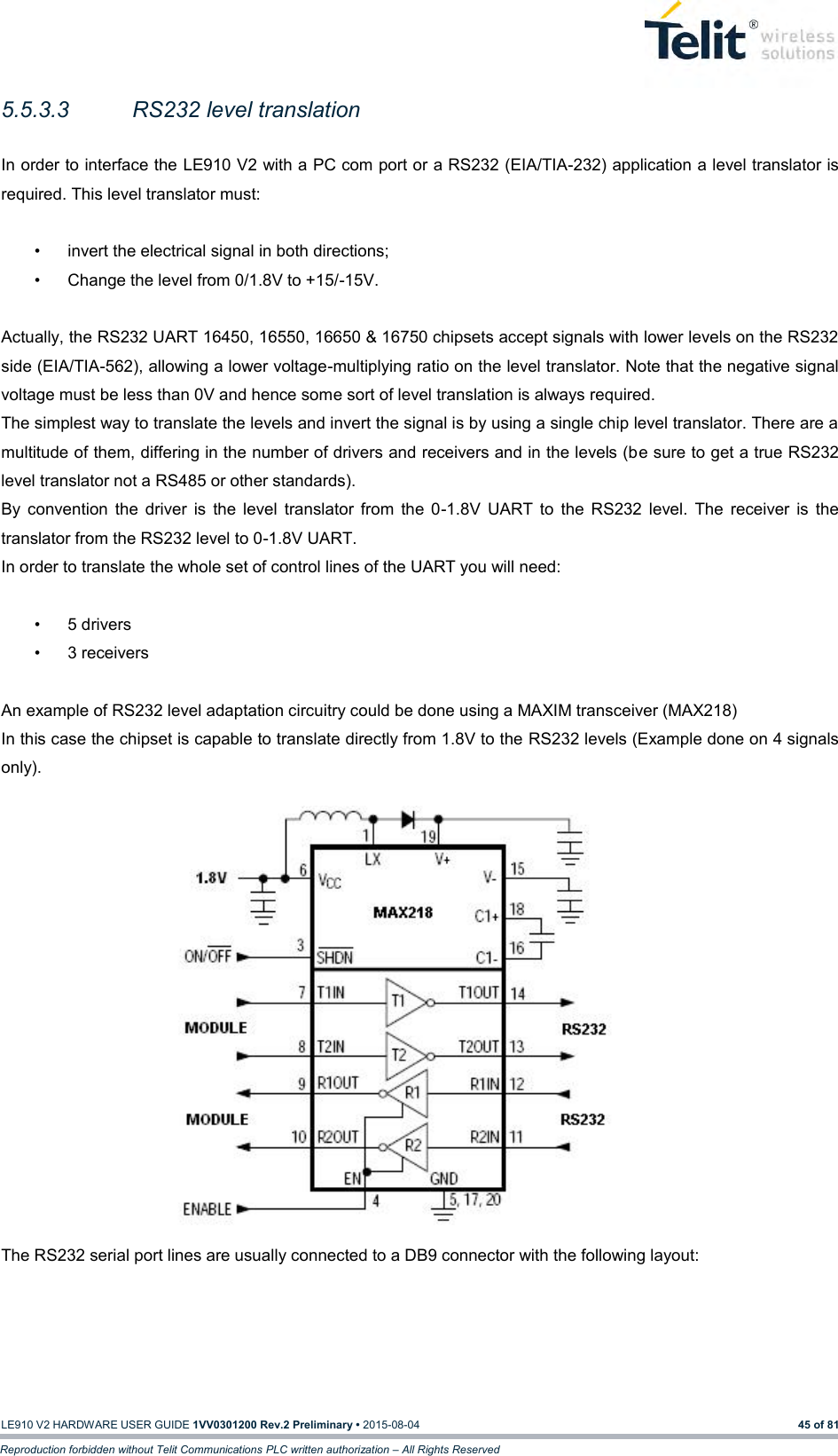
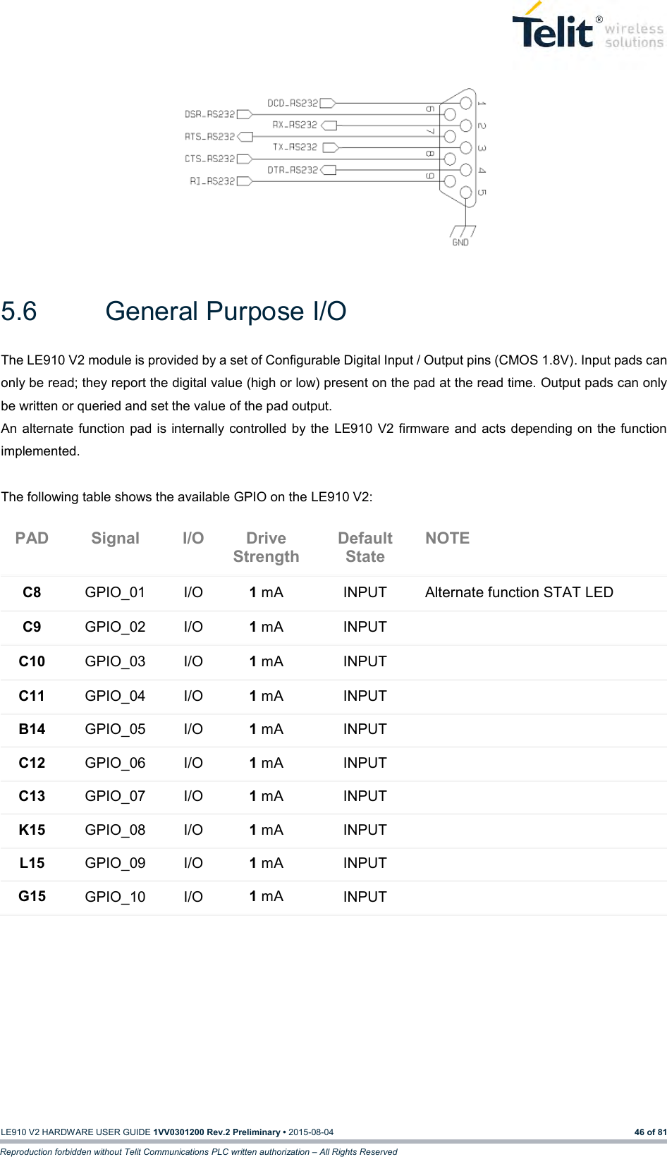
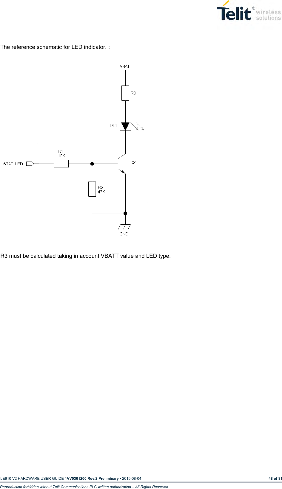
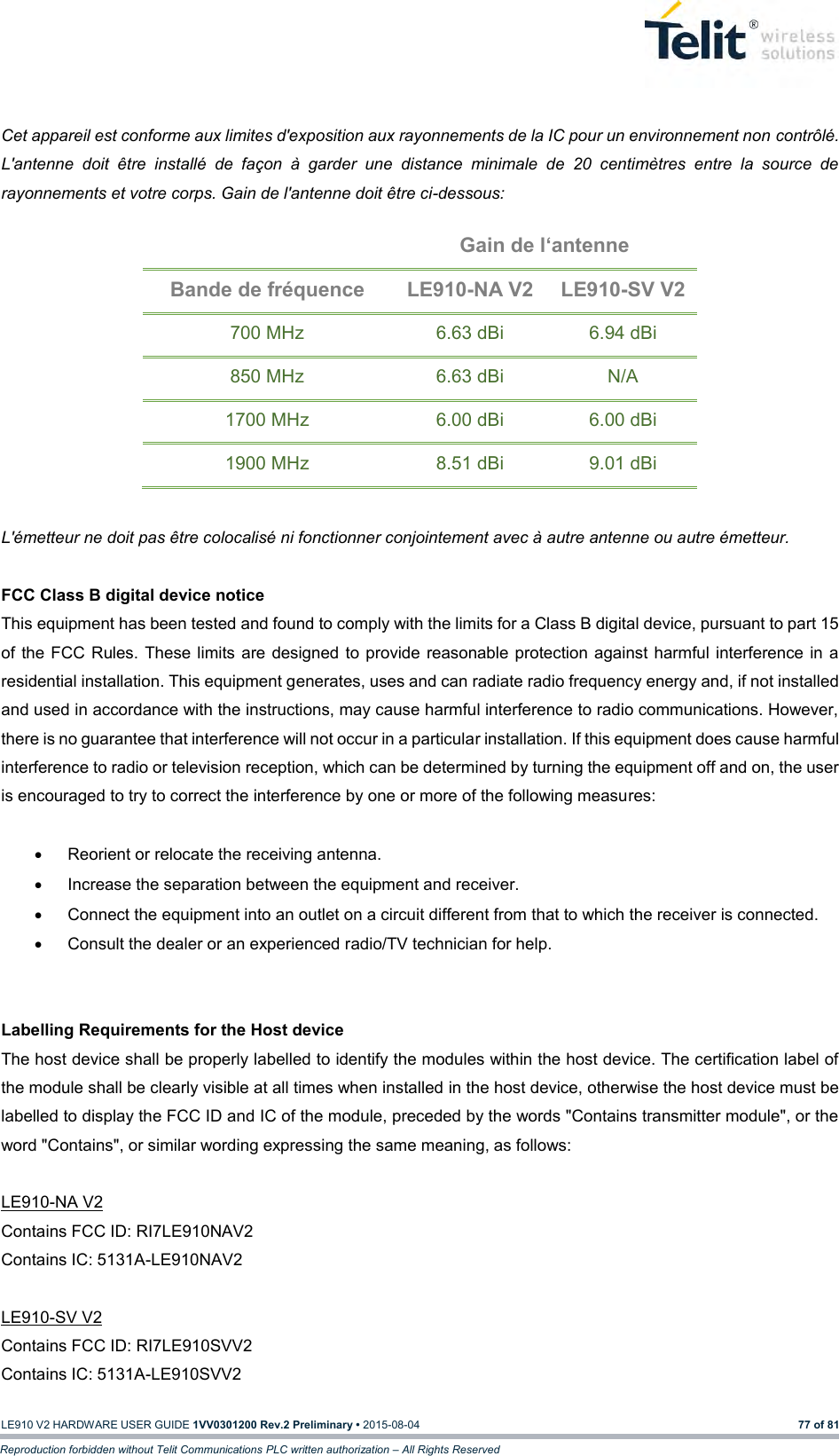
Tyco Safety Canada 17LE4010 LTE Cellular Alarm Communicator User Manual LE910 V2 Hardware User Guide

Digital Security Controls Ltd. LTE Cellular Alarm Communicator LE910 V2 Hardware User Guide

Contents

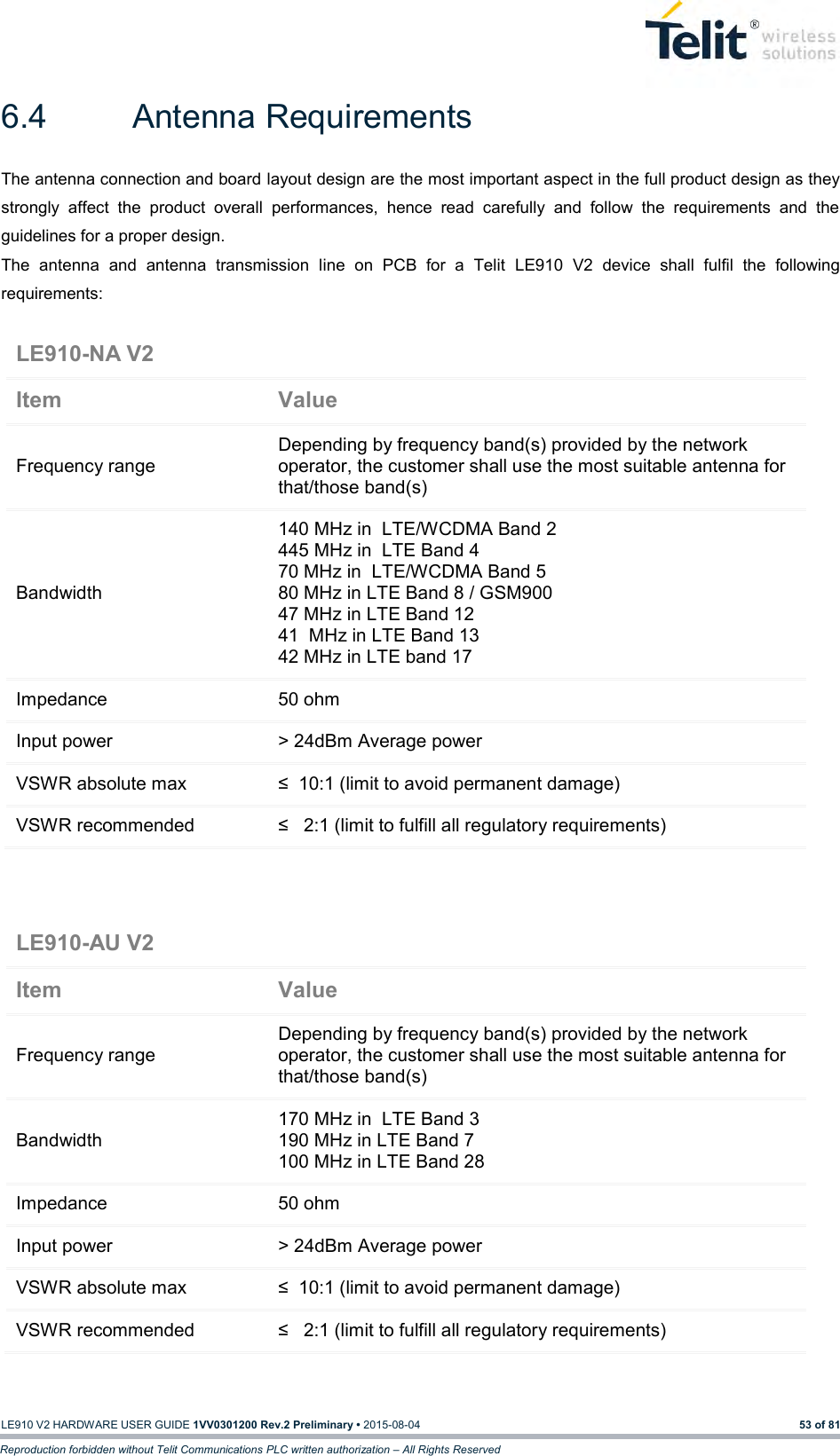
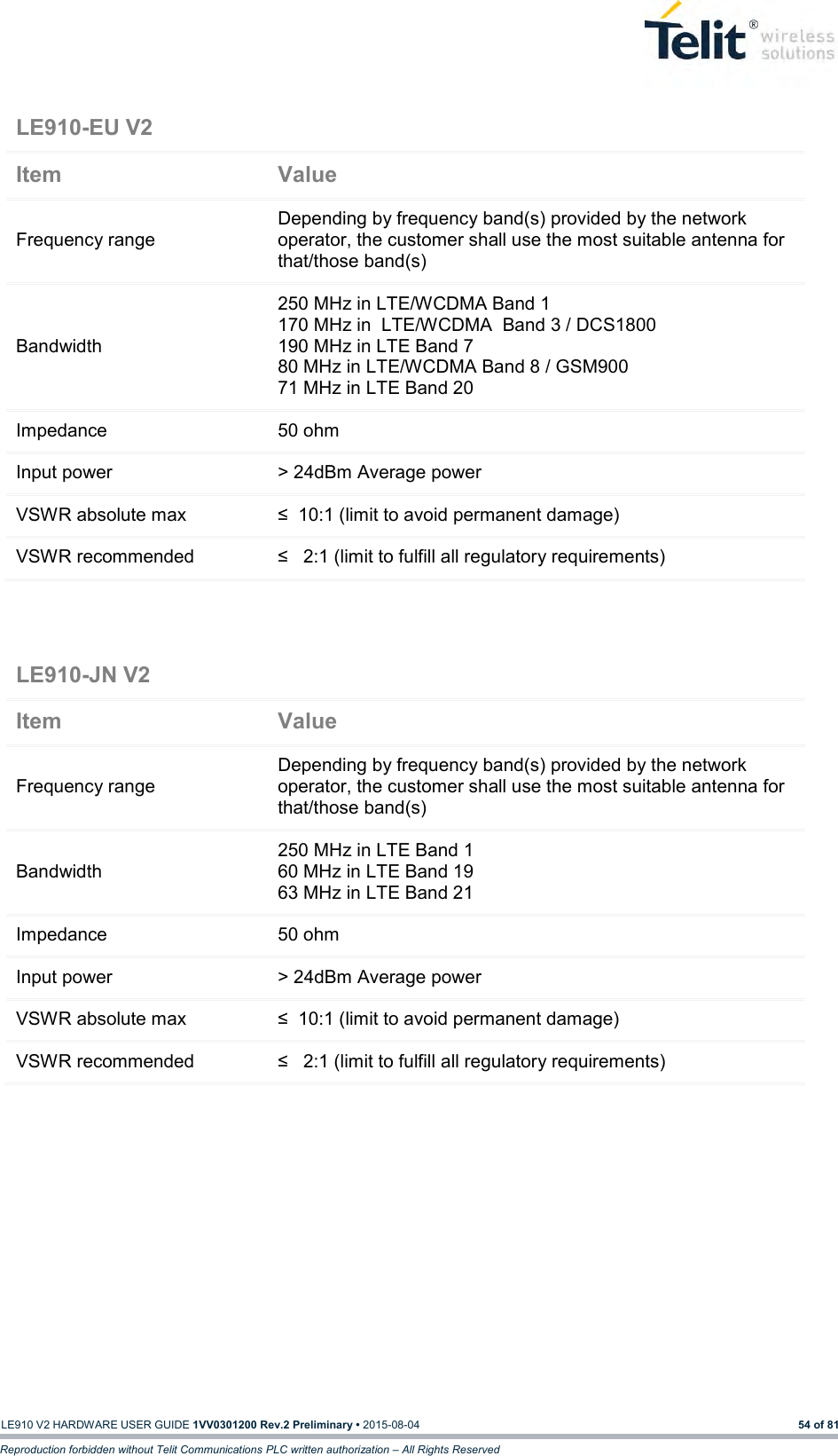
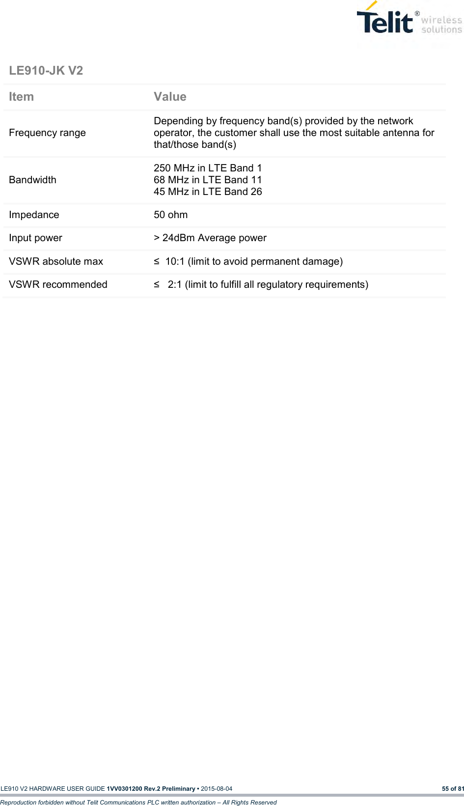
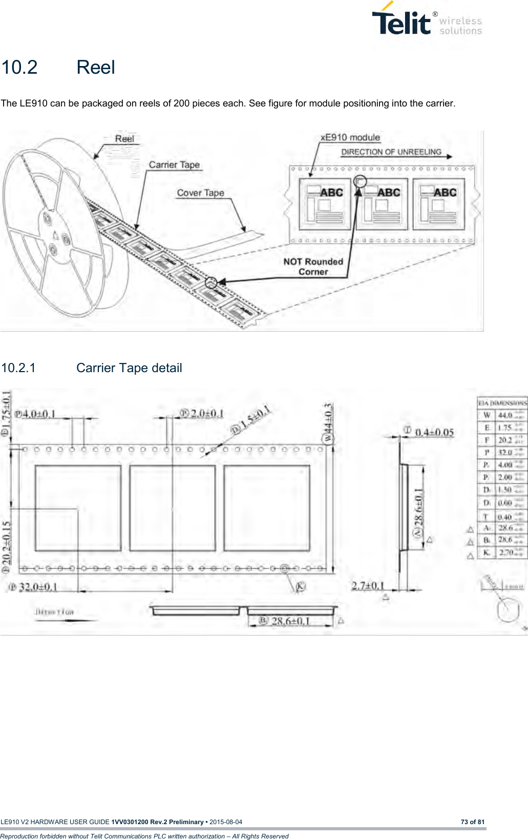
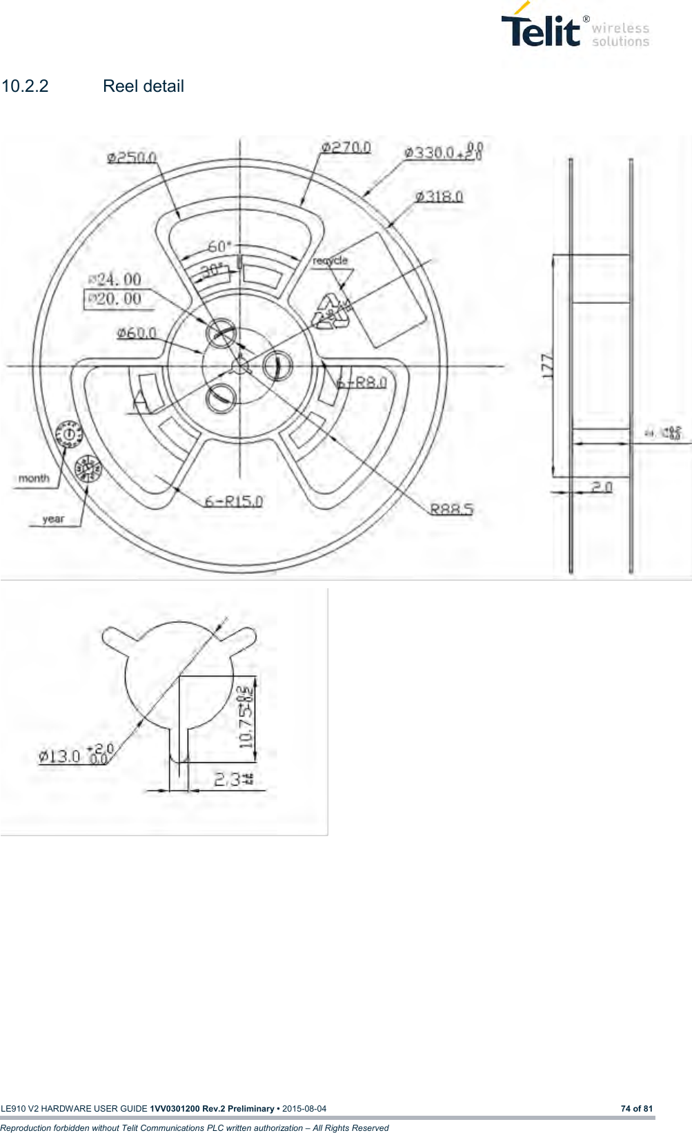
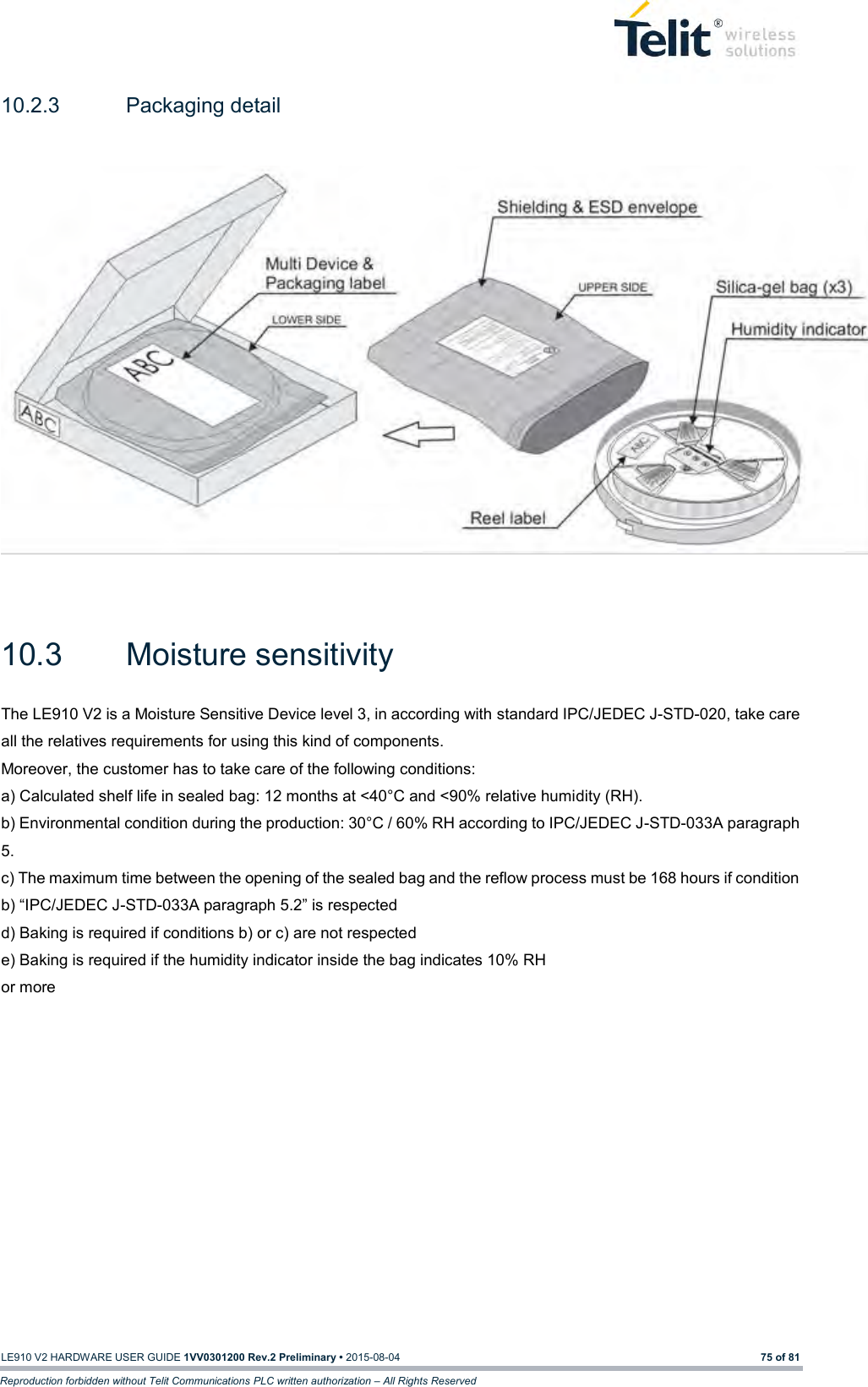
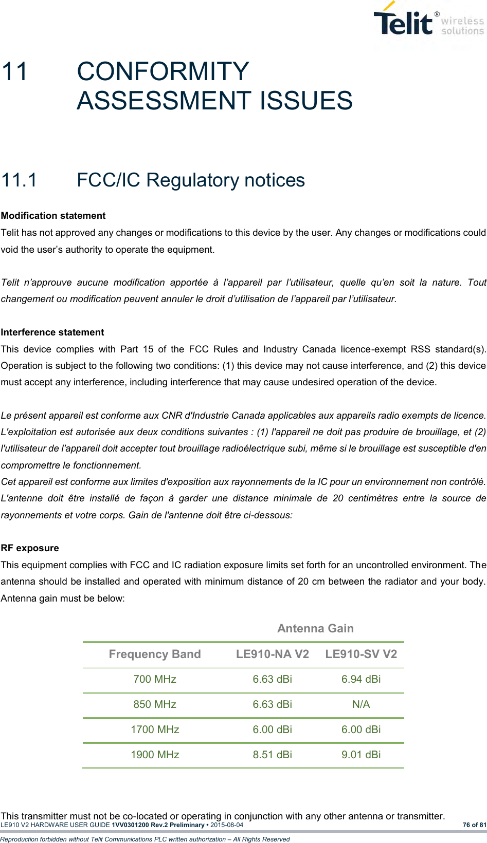
RI7LE910NAV2 User Manual

1VV0301200 Rev.2 - Preliminary  2015-08-04 LE910 V2 HARDWARE USER GUIDE
 LE910 V2 HARDWARE USER GUIDE 1VV0301200 Rev.2 Preliminary • 2015-08-04 2 of 81 Reproduction forbidden without Telit Communications PLC written authorization – All Rights Reserved APPLICABILITY TABLE PRODUCTS    LE910-NA V2    LE910-SV V2    LE910-EU V2    LE910-AU V2    LE910-JN V2    LE910-JK V2
 LE910 V2 HARDWARE USER GUIDE 1VV0301200 Rev.2 Preliminary • 2015-08-04 3 of 81 Reproduction forbidden without Telit Communications PLC written authorization – All Rights Reserved SPECIFICATIONS SUBJECT TO CHANGE WITHOUT NOTICE LEGAL NOTICE These  Specifications  are  general  guidelines  pertaining  to  product  selection  and  application  and  may  not  be appropriate  for  your  particular  project.  Telit  (which  hereinafter  shall  include,  its  agents,  licensors  and  affiliated companies)  makes  no  representation  as  to  the  particular  products  identified  in  this  document  and  makes  no endorsement of any product. Telit disclaims any warranties, expressed or implied, relating to these specifications, including without limitation, warranties or merchantability, fitness  for a particular purpose or satisfactory  quality. Without limitation, Telit reserves the right to make changes to any products described herein and to remove any product, without notice.   It  is  possible  that  this  document  may  contain  references  to,  or  information  about  Telit  products,  services  and programs, that are not available in your region. Such references or information must not be construed to mean that Telit intends to make available such products, services and programs in your area.    USE AND INTELLECTUAL PROPERTY RIGHTS These Specifications (and the products and services contained herein) are proprietary to Telit and its licensors and constitute the intellectual property of Telit (and its licensors). All title and intellectual property rights in and to the Specifications  (and the products and services contained herein)  is  owned  exclusively by Telit and its licensors.  Other than as expressly set forth herein, no license or other rights in or to the Specifications and intellectual property rights related thereto are granted to you.   Nothing in these Specifications shall, or shall be deemed to, convey license or any other right under Telit’s patents, copyright, mask work or other intellectual property rights or the rights of others.      You may not, without the express written permission of Telit:  (i) copy, reproduce, create derivative works of, reverse engineer, disassemble, decompile, distribute, merge or modify in any manner these Specifications or the products and components described herein; (ii) separate any component part of the products described herein, or separately use any component part thereof on any equipment, machinery, hardware or system; (iii) remove or destroy any proprietary  marking  or  legends  placed  upon  or  contained  within  the  products  or  their  components  or  these Specifications; (iv) develop methods to enable unauthorized parties to use the products or their components; and (v) attempt to reconstruct or discover any source code, underlying ideas, algorithms, file formats or programming or  interoperability  interfaces  of  the products  or  their components  by  any means  whatsoever.    No  part  of  these Specifications or any products or components described herein may be reproduced, transmitted, transcribed, stored in a retrieval system, or translated into any language or computer language, in any form or by any means, without the prior express written permission of Telit.   HIGH RISK MATERIALS Components, units, or third-party products contained or used with the      products described herein are NOT fault-tolerant and are NOT designed, manufactured, or intended for use as on-line control equipment in the following hazardous  environments  requiring  fail-safe  controls:  the  operation  of  Nuclear  Facilities,  Aircraft  Navigation  or
 LE910 V2 HARDWARE USER GUIDE 1VV0301200 Rev.2 Preliminary • 2015-08-04 4 of 81 Reproduction forbidden without Telit Communications PLC written authorization – All Rights Reserved Aircraft Communication Systems, Air Traffic Control, Life Support, or Weapons Systems (“High Risk Activities"). Telit, its licensors and its supplier(s) specifically disclaim any expressed or implied warranty of fitness for such High Risk Activities. TRADEMARKS You may not and may not allow others to use Telit or its third party licensors’ trademarks.  To the extent that any portion of the products, components and any accompanying documents contain proprietary and confidential notices or legends, you will not remove such notices or legends.   Copyright © Telit Communications PLC.
 LE910 V2 HARDWARE USER GUIDE 1VV0301200 Rev.2 Preliminary • 2015-08-04 5 of 81 Reproduction forbidden without Telit Communications PLC written authorization – All Rights Reserved CONTENTS 1 Introduction  8 1.1 Scope  8 1.2 Audience  8 1.3 Contact Information, Support  8 1.4 List of acronyms  9 1.5 Text Conventions  11 1.6 Related Documents  11 2 Overview  12 3 Pins Allocation  13 3.1 Pin-out 13 3.2 LGA Pads Layout  20 4 Power Supply  21 4.1 Power Supply Requirements  21 4.2 Power Consumption  22 4.3 General Design Rules  23 4.3.1 Electrical Design Guidelines  23 4.3.1.1 +5V Source Power Supply Design Guidelines  23 4.3.1.3 Battery Source Power Supply Design Guidelines  25 4.3.1.4 Thermal Design Guidelines  26 4.3.1.5 Power Supply PCB layout Guidelines  27 4.4 RTC Bypass out  29 4.5 VAUX Power Output  29 5 Digital Section  30 5.1 Logic Levels  30 5.2 Power on  31 5.3 Power off  36 5.4 Unconditional Shutdown  38 5.5 Communication ports  41 5.5.1 USB 2.0 HS  41 5.5.2 SPI  42 5.5.2.1 SPI Connections  42 5.5.3 Serial Ports  43 5.5.3.1 Modem serial port 1 (USIF0)  43
 LE910 V2 HARDWARE USER GUIDE 1VV0301200 Rev.2 Preliminary • 2015-08-04 6 of 81 Reproduction forbidden without Telit Communications PLC written authorization – All Rights Reserved 5.5.3.2 Modem serial port 2 (USIF1)  44 5.5.3.3 RS232 level translation  45 5.6 General Purpose I/O  46 5.6.1 Using a GPIO as INPUT  47 5.6.2 Using a GPIO as OUTPUT  47 5.6.3 Indication of network service availability  47 5.7 External SIM Holder  49 5.8 ADC Converter  49 6 RF Section  50 6.1 Bands Variants  50 6.2 TX Output Power  50 6.3 RX Sensitivity  51 6.4 Antenna Requirements  53 6.4.1 PCB design guidelines  56 6.4.2 PCB Guidelines in case of FCC Certification  57 6.4.2.1 Transmission line design  57 6.4.2.2 Transmission Line Measurements  58 6.4.2.3 Antenna Installation Guidelines  60 7 Audio Section Overview  64 7.1 Electrical Characteristics  64 7.2 Codec examples  64 8 Mechanical Design  65 8.1 Drawing  65 9 Application PCB Design  66 9.1 Footprint  66 9.2 PCB pad design  67 9.3 PCB pad dimensions  67 9.4 Stencil  69 9.5 Solder paste  69 9.6 Solder reflow  69 10 Packaging  71 10.1 Tray  71 10.2 Reel  73 10.2.1 Carrier Tape detail  73 10.2.2 Reel detail  74 10.2.3 Packaging detail  75 10.3 Moisture sensitivity  75
 LE910 V2 HARDWARE USER GUIDE 1VV0301200 Rev.2 Preliminary • 2015-08-04 7 of 81 Reproduction forbidden without Telit Communications PLC written authorization – All Rights Reserved 11 Conformity Assessment Issues  76 11.1 FCC/IC Regulatory notices  76 12 Safety Recommendations  79 12.1 READ CAREFULLY  79 13 Document History  80 13.1 Revisions  80
  LE910 V2 HARDWARE USER GUIDE 1VV0301200 Rev.2 Preliminary • 2015-08-04 8 of 81 Reproduction forbidden without Telit Communications PLC written authorization – All Rights Reserved 1  INTRODUCTION 1.1  Scope Scope of this document is to give a description of some hardware solutions useful for developing a product with the Telit LE910 V2 module.  1.2  Audience This document is intended for Telit customers, who are integrators, about to implement their applications using our LE910 V2 modules. 1.3  Contact Information, Support For general contact, technical support services, technical questions and report documentation errors contact Telit Technical Support at: TS-EMEA@telit.com  TS-AMERICAS@telit.com  TS-APAC@telit.com   Alternatively, use: http://www.telit.com/support   For detailed information about where you can buy the Telit modules or for recommendations on accessories and components visit: http://www.telit.com   Our aim is  to make this  guide as helpful as  possible. Keep us  informed of your  comments and suggestions for improvements. Telit appreciates feedback from the users of our information.
  LE910 V2 HARDWARE USER GUIDE 1VV0301200 Rev.2 Preliminary • 2015-08-04 9 of 81 Reproduction forbidden without Telit Communications PLC written authorization – All Rights Reserved 1.4  List of acronyms Acronym Description LTE Long Term Evolution RF Radio Frequency EMC Electromagnetic Compatibility FDD Frequency Division Duplexing EM Electromagnetic EMI Electromagnetic Interference PCB Printed Circuit Board USB Universal Serial Bus HS High Speed DTE Data Terminal Equipment UMTS Universal Mobile Telecommunication System WCDMA Wideband Code Division Multiple Access HSDPA High Speed Downlink Packet Access HSUPA High Speed Uplink Packet Access UART Universal Asynchronous Receiver Transmitter HSIC High Speed Inter Chip SIM Subscriber Identification Module SPI Serial Peripheral Interface ADC Analog – Digital Converter DAC Digital – Analog Converter I/O Input Output GPIO General Purpose Input Output CMOS Complementary Metal – Oxide Semiconductor MOSI Master Output – Slave Input MISO Master Input – Slave Output CLK Clock
  LE910 V2 HARDWARE USER GUIDE 1VV0301200 Rev.2 Preliminary • 2015-08-04 10 of 81 Reproduction forbidden without Telit Communications PLC written authorization – All Rights Reserved  Acronym Description DVI Digital Voice Interface MRDY Master Ready SRDY Slave Ready CS Chip Select RTC Real Time Clock ESR Equivalent Series Resistance VSWR Voltage Standing Wave Radio VNA Vector Network Analyzer
  LE910 V2 HARDWARE USER GUIDE 1VV0301200 Rev.2 Preliminary • 2015-08-04 11 of 81 Reproduction forbidden without Telit Communications PLC written authorization – All Rights Reserved 1.5  Text Conventions   Danger – This information MUST be followed or catastrophic equipment failure or bodily injury may occur.     Caution or Warning – Alerts the user to important points about integrating the module, if these points are not followed, the module and end user equipment may fail or malfunction.     Tip or Information – Provides advice and suggestions that may be useful when integrating the module.   All dates are in ISO 8601 format, i.e. YYYY-MM-DD.   1.6  Related Documents ●  Telit_xE910_Global_Form_Factor_Application_Note_r13 ●  Telit_Event_Monitor_Application_Note_r6 ●  Telit_SIM/USIM_Toolkit_Application_Note_r4 ●  Telit_Modem_Integration_Design_Guide_r0 ●  SIM Holder Design Guides, 80000NT10001a
  LE910 V2 HARDWARE USER GUIDE 1VV0301200 Rev.2 Preliminary • 2015-08-04 12 of 81 Reproduction forbidden without Telit Communications PLC written authorization – All Rights Reserved 2  OVERVIEW The aim of this document is the description of some hardware solutions useful for developing a product with the Telit LE910 V2 module. In this document all the basic functions of a mobile phone will be taken into account; for each one of them a proper hardware solution will be suggested and eventually the wrong solutions and common errors to be avoided will be evidenced.  Obviously  this  document  cannot  embrace  the  whole  hardware  solutions  and  products  that  may  be designed. The wrong solutions to be avoided shall be considered as mandatory, while the suggested hardware configurations shall not be considered mandatory, instead the information given shall be used as a guide and a starting point for properly developing your product with the Telit LE910 V2 module. For further hardware details that may not  be explained in this document refer  to the Telit  LE910 V2 Product Description document where all the hardware information is reported.    NOTE: (EN) The integration of the LE910 V2 cellular module within user application shall be done according to the design rules described in this manual.  (IT) L’integrazione del modulo cellulare LE910 V2 all’interno dell’applicazione dell’utente dovrà rispettare le indicazioni progettuali descritte in questo manuale.  (DE)  Die  Integration  des  LE910 V2  Mobilfunk-Moduls  in  ein  Gerät  muß gemäß der  in diesem Dokument beschriebenen Kunstruktionsregeln erfolgen.  (SL) Integracija LE910 V2 modula v uporabniški aplikaciji bo morala upoštevati projektna navodila, opisana v tem priročniku.  (SP) La utilización del modulo LE910 V2 debe ser conforme a los usos para los cuales ha sido deseñado descritos en este manual del usuario.  (FR) L’intégration du module cellulaire LE910 V2 dans l’application de l’utilisateur sera faite selon les règles de conception décrites dans ce manuel.  (HE)   The information presented in this document is believed to be accurate and reliable. However, no responsibility is assumed by Telit Communications S.p.A. for its use, nor any infringement of patents or other rights of third parties which may result from its use. No license is granted by implication or  otherwise under any patent rights of Telit Communications  S.p.A.  other than for circuitry embodied in Telit  products. This  document  is  subject  to change without notice. LE910 V2
  LE910 V2 HARDWARE USER GUIDE 1VV0301200 Rev.2 Preliminary • 2015-08-04 13 of 81 Reproduction forbidden without Telit Communications PLC written authorization – All Rights Reserved 3  PINS ALLOCATION 3.1  Pin-out Pin Signal I/O Function Type Comment USB HS 2.0 COMMUNICATION PORT B15 USB_D+ I/O USB differential Data (+)   C15 USB_D- I/O USB differential Data (-)   A13 VUSB I Power sense for the internal USB transceiver.   Asynchronous Serial Port (USIF0) - Prog. / Data + HW Flow Control N15 C103/TXD I Serial data input from DTE CMOS 1.8V  M15 C104/RXD O Serial data output to DTE CMOS 1.8V  M14 C108/DTR I Input for (DTR) from DTE CMOS 1.8V  L14 C105/RTS I Input for Request to send signal (RTS) from DTE CMOS 1.8V  P15 C106/CTS O Output for Clear to Send signal (CTS) to DTE CMOS 1.8V  N14 C109/DCD O Output for  (DCD) to DTE CMOS 1.8V  P14 C107/DSR O Output for  (DSR) to DTE CMOS 1.8V  R14 C125/RING O Output for Ring (RI) to DTE CMOS 1.8V  Asynchronous Auxiliary Serial Port (USIF1) D15 TX_AUX O Auxiliary UART (TX Data to DTE) CMOS 1.8V  E15 RX_AUX I Auxiliary UART (RX Data from DTE) CMOS 1.8V        SIM card interface A6 SIMCLK O External SIM signal – Clock 1.8 / 3V  A7 SIMRST O External SIM signal – Reset 1.8 / 3V
  LE910 V2 HARDWARE USER GUIDE 1VV0301200 Rev.2 Preliminary • 2015-08-04 14 of 81 Reproduction forbidden without Telit Communications PLC written authorization – All Rights Reserved A5 SIMIO I/O External SIM signal – Data I/O 1.8 / 3V  A4 SIMIN I External SIM signal – Presence (active low) CMOS 1.8 Internal pullup 47K A3 SIMVCC - External SIM signal – Power supply for the SIM 1.8 / 3V  Digital Voice Interface (DVI) B9 DVI_WA0 I/O Digital Audio Interface (WA0) 1.8V  B6 DVI_RX I Digital Audio Interface (RX) 1.8V  B7 DVI_TX I/O Digital Audio Interface (TX) 1.8V  B8 DVI_CLK I/O Digital Audio Interface (CLK) 1.8V  SPI      D15 SPI_MOSI I SPI MOSI CMOS 1.8V  E15 SPI_MISO O SPI_MISO CMOS 1.8V  F15 SPI_CLK I SPI Clock CMOS 1.8V  H15 SPI_MRDY I SPI_MRDY CMOS 1.8V  J15 SPI_SRDY O SPI_SRDY CMOS 1.8V  DIGITAL IO C8 GPIO_01 I/O GPIO_01 /STAT LED CMOS 1.8V STAT LED is alternate function C9 GPIO_02 I/O GPIO_02 CMOS 1.8V  C10 GPIO_03 I/O GPIO_03 CMOS 1.8V  C11 GPIO_04 I/O GPIO_04 CMOS 1.8V  B14 GPIO_05 I/O GPIO_05 CMOS 1.8V  C12 GPIO_06 I/O GPIO_06 CMOS 1.8V  C13 GPIO_07 I/O GPIO_07 CMOS 1.8V  K15 GPIO_08 I/O GPIO_08 CMOS 1.8V  L15 GPIO_09 I/O GPIO_09 CMOS 1.8V  G15 GPIO_10 I/O GPIO_10 CMOS 1.8V  ADC
  LE910 V2 HARDWARE USER GUIDE 1VV0301200 Rev.2 Preliminary • 2015-08-04 15 of 81 Reproduction forbidden without Telit Communications PLC written authorization – All Rights Reserved B1 ADC_IN1 AI Analog / Digital converter input A/D Accepted values 0 to 1.2V DC RF SECTION K1 ANTENNA I/O GSM/EDGE/UMTS  Antenna (50 ohm) RF  F1 ANT_DIV I Antenna Diversity Input (50 ohm) RF  Miscellaneous Functions R13 HW_SHUTDOWN* I HW Unconditional Shutdown 1.8V Active low R12 ON_OFF* I Input command for power ON 1.8V Active low C14 VRTC I VRTC Backup capacitor Power backup for the embedded RTC supply (1.8V) R11 VAUX/PWRMON O Supply Output for external accessories / Power ON Monitor 1.8V  Power Supply M1 VBATT - Main power supply (Baseband) Power  M2 VBATT - Main power supply (Baseband) Power  N1 VBATT_PA - Main power supply (Radio PA) Power  N2 VBATT_PA - Main power supply (Radio PA) Power  P1 VBATT_PA - Main power supply (Radio PA) Power  P2 VBATT_PA - Main power supply (Radio PA) Power  E1 GND - Ground Power  G1 GND - Ground Power  H1 GND - Ground Power  J1 GND - Ground Power  L1 GND - Ground Power  A2 GND - Ground Power  E2 GND - Ground Power
  LE910 V2 HARDWARE USER GUIDE 1VV0301200 Rev.2 Preliminary • 2015-08-04 16 of 81 Reproduction forbidden without Telit Communications PLC written authorization – All Rights Reserved F2 GND - Ground Power  G2 GND - Ground Power  H2 GND - Ground Power  J2 GND - Ground Power  K2 GND - Ground Power  L2 GND - Ground Power  R2 GND - Ground Power  M3 GND - Ground Power  N3 GND - Ground Power  P3 GND - Ground Power  R3 GND - Ground Power  D4 GND - Ground Power  M4 GND - Ground Power  N4 GND - Ground Power  P4 GND - Ground Power  R4 GND - Ground Power  N5 GND - Ground Power  P5 GND - Ground Power  R5 GND - Ground Power  N6 GND - Ground Power  P6 GND - Ground Power  R6 GND - Ground Power  P8 GND - Ground Power  R8 GND - Ground Power  P9 GND - Ground Power  P10 GND - Ground Power  R10 GND - Ground Power  M12 GND - Ground Power  B13 GND - Ground Power  P13 GND - Ground Power
  LE910 V2 HARDWARE USER GUIDE 1VV0301200 Rev.2 Preliminary • 2015-08-04 17 of 81 Reproduction forbidden without Telit Communications PLC written authorization – All Rights Reserved E14 GND - Ground Power  RESERVED C1 RESERVED - RESERVED   D1 RESERVED - RESERVED   B2 RESERVED - RESERVED   C2 RESERVED - RESERVED   D2 RESERVED - RESERVED   B3 RESERVED - RESERVED   C3 RESERVED - RESERVED   D3 RESERVED - RESERVED   E3 RESERVED - RESERVED   F3 RESERVED - RESERVED   G3 RESERVED - RESERVED   H3 RESERVED - RESERVED   J3 RESERVED - RESERVED   K3 RESERVED - RESERVED   L3 RESERVED - RESERVED   B4 RESERVED - RESERVED   C4 RESERVED - RESERVED   B5 RESERVED - RESERVED   C5 RESERVED - RESERVED   C6 RESERVED - RESERVED   C7 RESERVED - RESERVED   N7 RESERVED - RESERVED   P7 RESERVED - RESERVED   N8 RESERVED - RESERVED   N9 RESERVED - RESERVED   A10 RESERVED - RESERVED   N10 RESERVED - RESERVED   N11 RESERVED - RESERVED
  LE910 V2 HARDWARE USER GUIDE 1VV0301200 Rev.2 Preliminary • 2015-08-04 18 of 81 Reproduction forbidden without Telit Communications PLC written authorization – All Rights Reserved P11 RESERVED - RESERVED   B12 RESERVED - RESERVED   D12 RESERVED - RESERVED   N12 RESERVED - RESERVED   P12 RESERVED - RESERVED   F14 RESERVED - RESERVED   G14 RESERVED - RESERVED   H14 RESERVED - RESERVED   J14 RESERVED - RESERVED   K14 RESERVED - RESERVED   N13 RESERVED - RESERVED   L13 RESERVED - RESERVED   J13 RESERVED - RESERVED   M13 RESERVED - RESERVED   K13 RESERVED - RESERVED   H13 RESERVED - RESERVED   G13 RESERVED - RESERVED   F13 RESERVED - RESERVED   B11 RESERVED - RESERVED   B10 RESERVED - RESERVED   A9 RESERVED - RESERVED   A8 RESERVED - RESERVED   E13 RESERVED - RESERVED   D13 RESERVED - RESERVED   D14 RESERVED - RESERVED   A14 RESERVED - RESERVED   A12 RESERVED - RESERVED   A11 RESERVED - RESERVED   H15 RESERVED - RESERVED   F15 RESERVED - RESERVED
  LE910 V2 HARDWARE USER GUIDE 1VV0301200 Rev.2 Preliminary • 2015-08-04 19 of 81 Reproduction forbidden without Telit Communications PLC written authorization – All Rights Reserved     WARNING: Reserved pins must not be connected.    K15 RESERVED - RESERVED   J15 RESERVED - RESERVED
  LE910 V2 HARDWARE USER GUIDE 1VV0301200 Rev.2 Preliminary • 2015-08-04 20 of 81 Reproduction forbidden without Telit Communications PLC written authorization – All Rights Reserved 3.2  LGA Pads Layout  TOP VIEW    A B C D E F G  H J K L M N P R    1   ADC_IN1 RES RES GND ANT_DIV GND GND GND ANT GND VBATT VBATT_PA VBATT_PA     2 GND RES RES RES GND GND GND GND GND GND GND VBATT VBATT_PA VBATT_PA GND   3 SIMVCC RES RES RES RES RES RES RES RES RES RES GND GND GND GND   4 SIMIN RES RES GND               GND GND GND GND   5 SIMIO RES RES                   GND GND GND   6 SIMCLK DVI_RX RES                   GND GND GND   7 SIMRST DVI_TX RES                   RES RES RES   8 RES DVI_CLK GPIO_01                   RES GND GND   9 RES DVI_WA0 GPIO_02                   RES GND RES   10 RES RES GPIO_03                   RES GND GND   11 RES RES GPIO_04                   RES RES VAUX/PWRMON   12 RES RES GPIO_06 RES               GND RES RES ON_OFF*   13 VUSB GND GPIO_07 RES RES RES RES RES RES RES RES RES RES GND HW_SHUTDOWN*   14 RES GPIO_05 VRTC RES GND RES RES RES RES RES C105/RTS C108/DTR C109/DCD C107/DSR C125/RING   15   USB_D+ USB_D- TX AUX RX AUX SPI_CLK GPIO_10 SPI_MRDY SPI_SRDY GPIO_08 GPIO_09 C104/RXD C103/TXD C106/CTS
  LE910 V2 HARDWARE USER GUIDE 1VV0301200 Rev.2 Preliminary • 2015-08-04 21 of 81 Reproduction forbidden without Telit Communications PLC written authorization – All Rights Reserved 4  POWER SUPPLY The power supply circuitry and board layout are a very important part in the full  product design and they strongly reflect on the product overall performances, hence read carefully the requirements and the guidelines that will follow for a proper design. 4.1  Power Supply Requirements The  external  power  supply  must  be  connected  to  VBATT  &  VBATT_PA  signals  and  must  fulfil  the  following requirements: Power Supply Value Nominal Supply Voltage 3.8V Normal Operating Voltage Range 3.40 V÷ 4.20 V Extended Operating Voltage Range 3.10 V÷ 4.50 V     NOTE: The  Operating  Voltage  Range  MUST  never  be  exceeded;  care  must  be  taken  when designing the application’s power supply section to avoid having an excessive voltage drop. If the voltage drop is exceeding the limits it could cause a Power Off of the module. The Power supply must be higher than 3.10 V to power on the module.  Overshoot  voltage  (regarding  MAX  Extended  Operating  Voltage)  and  drop  in  voltage (regarding MIN Extended Operating Voltage) MUST never be exceeded;  The “Extended Operating Voltage Range” can be used only with completely assumption and application of the HW User guide suggestions.
  LE910 V2 HARDWARE USER GUIDE 1VV0301200 Rev.2 Preliminary • 2015-08-04 22 of 81 Reproduction forbidden without Telit Communications PLC written authorization – All Rights Reserved 4.2  Power Consumption The reported values in the following table has to be considered preliminary: Mode Average (mA) Mode Description Switched Off 94uA Module supplied but switched off AT+CFUN=5 1.3mA  (WCDMA) EGPRS mode 550mA Typical (max UL throughput, class 33, 3.80V supply) HSUPA mode 550mA Typical (max UL throughput, 3.80V supply) LTE mode 550mA Typical (max UL throughput, 3.80V supply)    NOTE: The electrical design for the Power supply should be made ensuring it will be capable of a peak current output of at least: 0.8 A for WCDMA and LTE mode (3.80V supply). 2A for GSM mode (3.80V supply).
  LE910 V2 HARDWARE USER GUIDE 1VV0301200 Rev.2 Preliminary • 2015-08-04 23 of 81 Reproduction forbidden without Telit Communications PLC written authorization – All Rights Reserved 4.3  General Design Rules The principal guidelines for the Power Supply Design embrace three different design steps:   the electrical design   the thermal design  the PCB layout. 4.3.1  Electrical Design Guidelines The electrical design of the power supply depends strongly from the power source where this power is drained. We will distinguish them into three categories:   +5V input   (typically PC internal regulator output)   +12V input (typically automotive)   Battery  4.3.1.1  +5V Source Power Supply Design Guidelines   The desired output for the power  supply  is  3.8V,  hence there's  not a big difference between the input source and the desired output and a linear regulator can be used. A switching power supply will not be suited because of the low drop out requirements.   When  using  a  linear  regulator,  a  proper  heat  sink  shall  be  provided  in  order  to  dissipate  the  power generated.   A Bypass low ESR capacitor of adequate capacity must be provided in order to cut the current absorption peaks close to the Module, a 100μF capacitor is usually suited.   Make sure the low ESR capacitor on the power supply output rated at least 10V.  An example of linear regulator with 5V input is:
  LE910 V2 HARDWARE USER GUIDE 1VV0301200 Rev.2 Preliminary • 2015-08-04 24 of 81 Reproduction forbidden without Telit Communications PLC written authorization – All Rights Reserved  4.3.1.2  + 12V input Source Power Supply Design Guidelines    The desired output for the power supply is 3.8V, hence due to the big difference between the input source and the desired output, a linear regulator is not suited and shall not be used. A switching power supply will be preferable because of its better efficiency.   When using a switching regulator, a 500kHz or more switching frequency regulator is preferable because of its smaller inductor size and its faster transient response. This allows the regulator to respond quickly to the current peaks absorption.    In any case the frequency and Switching design selection is related to the application to be developed due to the fact the switching frequency could also generate EMC interferences.   For car PB battery the input voltage can rise up to 15,8V and this should be kept in mind when choosing components: all components in the power supply must withstand this voltage.   A Bypass low ESR capacitor of adequate capacity must be provided in order to cut the current absorption peaks, a 100μF capacitor is usually suited.   Make sure the low ESR capacitor on the power supply output is rated at least 10V.   For Car applications a spike protection diode should be inserted close to the power input, in order to clean the supply from spikes.   An example of switching regulator with 12V input is in the below schematic:
  LE910 V2 HARDWARE USER GUIDE 1VV0301200 Rev.2 Preliminary • 2015-08-04 25 of 81 Reproduction forbidden without Telit Communications PLC written authorization – All Rights Reserved 4.3.1.3  Battery Source Power Supply Design Guidelines    The desired nominal output for the power supply is 3.8V and the maximum voltage allowed is 4.2V, hence a single 3.7V Li-Ion cell battery type is suited for supplying the power to the Telit LE910 V2 module.    A Bypass low ESR capacitor of adequate capacity must be provided in order to cut the current absorption peaks, a 100μF tantalum capacitor is usually suited.   Make sure the low ESR capacitor (usually a tantalum one) is rated at least 10V.   A protection diode should be inserted close to the power input, in order to save the LE910 V2 from power polarity inversion. Otherwise the battery connector should be done in a way to avoid polarity inversions when connecting the battery.   The battery must be rated to supply peaks of current up to 0.8 A for LTE and WCDMA mode and 2A for GSM mode.       NOTE: DON'T USE any Ni-Cd, Ni-MH, and Pb battery types directly connected with LE910 V2. Their use can lead to overvoltage on the LE910 V2 and damage it. USE ONLY Li-Ion battery types.
  LE910 V2 HARDWARE USER GUIDE 1VV0301200 Rev.2 Preliminary • 2015-08-04 26 of 81 Reproduction forbidden without Telit Communications PLC written authorization – All Rights Reserved  4.3.1.4  Thermal Design Guidelines  Worst case as reference values for thermal design of LE910 V2 are:    Average current consumption: 800 mA   Supply voltage: 3.80V        NOTE: Make PCB design in order to have the best connection of GND pads to large surfaces.    NOTE: The LE910 V2 includes a function to prevent overheating.
  LE910 V2 HARDWARE USER GUIDE 1VV0301200 Rev.2 Preliminary • 2015-08-04 27 of 81 Reproduction forbidden without Telit Communications PLC written authorization – All Rights Reserved 4.3.1.5  Power Supply PCB layout Guidelines  As seen on the electrical design guidelines the power supply shall have a low ESR capacitor on the output to cut the current peaks on the input to protect the supply from spikes The placement of this component is crucial for the correct working of the circuitry. A misplaced component can be useless or can even decrease the power supply performances.   The Bypass low ESR capacitor must be placed close to the Telit LE910 V2 power input pads or in the case the power supply is a switching type it can be placed close to the inductor to cut the ripple provided the PCB trace from the capacitor to the LE910 V2 is wide enough to ensure a dropless connection even during an 0.8 A current peak.    The protection diode must be placed close to the input connector where the power source is drained.    The PCB traces from the input connector to the power regulator IC must be wide enough to ensure  no voltage drops occur when an 2 A current peak is absorbed (worst case of GSM mode).     The PCB traces to the LE910 V2 and the Bypass capacitor must be wide enough to ensure no significant voltage  drops occur. This  is for the  same  reason  as previous point. Try to keep this  trace as short as possible.    To reduce the EMI due to switching, it is important to keep very small the mesh involved; thus the input capacitor, the output diode (if not embodied in the IC) and the regulator have to form a very small loop.This is done in order to reduce the radiated field (noise) at the switching frequency (100-500 kHz usually).    A dedicated ground for the Switching regulator separated by the common ground plane is suggested.    The placement of the power supply on the board should be done in such a way to guarantee that the high current  return  paths  in  the  ground  plane  are  not  overlapped  to  any  noise  sensitive  circuitry  as  the microphone amplifier/buffer or earphone amplifier.    The  power  supply  input  cables  should  be  kept  separate  from  noise  sensitive  lines  such  as microphone/earphone cables.    The insertion of EMI filter on VBATT pins is suggested in those designs where antenna is placed close to battery  or  supply  lines.  A  ferrite  bead  like  Murata  BLM18EG101TN1  or  Taiyo  Yuden  P/N FBMH1608HM101 can be used for this purpose.
  LE910 V2 HARDWARE USER GUIDE 1VV0301200 Rev.2 Preliminary • 2015-08-04 28 of 81 Reproduction forbidden without Telit Communications PLC written authorization – All Rights Reserved The below figure shows the recommended circuit:
  LE910 V2 HARDWARE USER GUIDE 1VV0301200 Rev.2 Preliminary • 2015-08-04 29 of 81 Reproduction forbidden without Telit Communications PLC written authorization – All Rights Reserved 4.4  RTC Bypass out The VRTC pin brings out the Real Time Clock supply, which is separate from the rest of the digital part, allowing having only RTC going on when all the other parts of the device are off. To this power output a backup capacitor can be added in order to increase the RTC autonomy during power off of the battery. NO Devices must be powered from this pin.  In order to keep the RTC active when VBATT is not supplied it is possible to back up the RTC section connecting a backup circuit to the related VRTC signal (pad C14 on module’s Pinout).  For  additional  details  on  the Backup  solutions  please  refer  to  the  related  application  note  (xE910  RTC Backup Application Note)  4.5  VAUX Power Output A regulated power supply output is provided in order to supply small devices from the module. The signal is present on Pad R11 and it is in common with the PWRMON (module powered ON indication) function. This output is always active when the module is powered ON.  The operating range characteristics of the supply are: Item Min Typical Max Output voltage 1.78V 1.80V 1.82V Output current - - 60mA Output bypass capacitor (inside the module)  1uF
  LE910 V2 HARDWARE USER GUIDE 1VV0301200 Rev.2 Preliminary • 2015-08-04 30 of 81 Reproduction forbidden without Telit Communications PLC written authorization – All Rights Reserved 5  DIGITAL SECTION 5.1  Logic Levels  ABSOLUTE MAXIMUM RATINGS – NOT FUNCTIONAL:   OPERATING RANGE - INTERFACE LEVELS (1.8V CMOS): Parameter Min Max Input high level 1.5V 1.9V Input low level 0V 0.35V Output high level 1.6V 1.9V Output low level 0V 0.2V   OPERATING RANGE - INTERFACE LEVELS (1.2V CMOS): Parameter Min Max Input high level 0.9V 1.3V Input low level 0V 0.3V Output high level 1V 1.3V Output low level 0V 0.1V   CURRENT CHARACTERISTICS: Parameter AVG Output Current 1mA Input Current 1uA Parameter Min Max Input level on any digital pin (CMOS 1.8) with respect to ground -0.3V 2.1V Input level on any digital pin (CMOS 1.2) with respect to ground -0.3V 1.4V
  LE910 V2 HARDWARE USER GUIDE 1VV0301200 Rev.2 Preliminary • 2015-08-04 31 of 81 Reproduction forbidden without Telit Communications PLC written authorization – All Rights Reserved 5.2  Power on To turn on the LE910 V2 the pad ON_OFF* must be tied low for at least 5 seconds and then released. The maximum current that can be drained from the ON_OFF* pad is 0,1 mA. A simple circuit to do it is:    NOTE: Don't use any pull up resistor on the ON_OFF* line, it is internally pulled up. Using pull up resistor may bring to latch up problems on the LE910 V2 power regulator and improper power on/off of the module. The line ON_OFF* must be connected only in open collector or open drain configuration.  In this document all the lines that are inverted, hence have active low signals are labelled with a name that ends with”#",”*” or with a bar over the name.  To check if the device has powered on, the hardware line PWRMON should be monitored.  It  is  mandatory  to  avoid  sending  data  to  the  serial  ports  during  the  first  200ms  of  the module start-up.
  LE910 V2 HARDWARE USER GUIDE 1VV0301200 Rev.2 Preliminary • 2015-08-04 32 of 81 Reproduction forbidden without Telit Communications PLC written authorization – All Rights Reserved A flow chart showing the proper turn on procedure is displayed below:                                             “Modem ON Proc” START VBATT > 3.10V ? ON_OFF* = LOW PWRMON=ON ? Delay = 5 sec ON_OFF* = HIGH GO TO “HW Shutdown Unconditional” PWRMON=ON ? Delay = 1 sec GO TO “Start AT Commands”” “Modem ON Proc” END N N Y Y Y N
  LE910 V2 HARDWARE USER GUIDE 1VV0301200 Rev.2 Preliminary • 2015-08-04 33 of 81 Reproduction forbidden without Telit Communications PLC written authorization – All Rights Reserved A flow chart showing the AT commands managing procedure is displayed below:                       NOTE: In order to avoid a back powering effect it is recommended to avoid having any HIGH logic level signal applied to the digital pins of the LE910 V2 when the module is powered off or during an ON/OFF transition.     “Start AT CMD” START Delay = 300 msec Enter AT <CR> GO TO “HW Shutdown Unconditional” AT answer in 1 sec ? GO TO “Modem ON Proc.” “Start AT CMD” END Y N
  LE910 V2 HARDWARE USER GUIDE 1VV0301200 Rev.2 Preliminary • 2015-08-04 34 of 81 Reproduction forbidden without Telit Communications PLC written authorization – All Rights Reserved  For example: 1- Let's assume you need to drive the ON_OFF* pad with a totem pole output of a +3/5 V microcontroller (uP_OUT1):              2- Let's assume you need to drive the ON_OFF* pad directly with an ON/OFF button:
  LE910 V2 HARDWARE USER GUIDE 1VV0301200 Rev.2 Preliminary • 2015-08-04 35 of 81 Reproduction forbidden without Telit Communications PLC written authorization – All Rights Reserved    WARNING It is recommended to set the ON_OFF* line LOW to power on the module only after VBATT is higher than 3.10V. In case this condition it is not satisfied you could use the HW_SHUTDOWN* line to recover it and then restart the power on activity using the ON_OFF * line. An example of this is described in the following diagram.     Power ON diagram: After HW_SHUTSDOWN* is released you could again use the ON_OFF* line to power on the module.
  LE910 V2 HARDWARE USER GUIDE 1VV0301200 Rev.2 Preliminary • 2015-08-04 36 of 81 Reproduction forbidden without Telit Communications PLC written authorization – All Rights Reserved 5.3  Power off Turning off of the device can be done in two ways: •  via  AT command (see LE910 V2 Software User Guide, AT#SHDN) •  by tying low pin ON_OFF*  Either ways, the device issues a detach request to network informing that the device will not be reachable any more.  To turn OFF the LE910 V2 the pad ON_OFF* must be tied low for at least 3 seconds and then released.    NOTE: To  check  if  the  device  has  been  powered  off,  the  hardware  line  PWRMON  must  be monitored. The device is powered off when PWRMON goes low.  In order to avoid a back powering effect it is recommended to avoid having any HIGH logic level signal applied to the digital pins of the LE910 V2 when the module is powered off or during an ON/OFF transition.
  LE910 V2 HARDWARE USER GUIDE 1VV0301200 Rev.2 Preliminary • 2015-08-04 37 of 81 Reproduction forbidden without Telit Communications PLC written authorization – All Rights Reserved The following flow chart shows the proper turn off procedure:      “Modem OFF Proc.” START ON_OFF* = LOW PWRMON=ON? Delay >= 3 sec ON_OFF* = HIGH PWRMON=ON? GO TO “HW SHUTDOWN Unconditional” “Modem OFF Proc.” END N Y Y N OFF Mode AT#SHDN Looping for more than 15s? Y N Key AT
  LE910 V2 HARDWARE USER GUIDE 1VV0301200 Rev.2 Preliminary • 2015-08-04 38 of 81 Reproduction forbidden without Telit Communications PLC written authorization – All Rights Reserved 5.4  Unconditional Shutdown HW_SHUTDOWN*  is used  to  unconditionally  shutdown  the  LE910  V2.  Whenever  this  signal  is  pulled  low,  the LE910 V2 is reset. When the device is reset it stops any operation. After the release of the line, the LE910 V2 is unconditionally  shut  down,  without  doing  any  detach  operation  from  the  network  where  it  is  registered.  This behaviour is not a proper shut down because any WCDMA device is requested to issue a detach request on turn off. The HW_SHUTDOWN* is internally controlled on start-up to achieve always a proper power-on reset sequence, so there's no need to control this pin on start-up.  To  unconditionally  shutdown  the  LE910  V2,  the  pad  HW_SHUTDOWN*  must  be  tied  low  for  at  least  200 milliseconds and then released. The signal is internally pulled up so the pin can be left floating if not used. If used, then it must always be connected with an open collector transistor, to permit to the internal circuitry the power on reset and under voltage lockout functions.  PIN DESCRIPTION Signal Function I/O PAD HW_SHUTDOWN* Unconditional Shutdown of the Module I R13    OPERATING LEVELS Signal Status Min Max HW_SHUTDOWN* Input high 1.5V 1.9V HW_SHUTDOWN* Input Low 0V 0.35V       WARNING: The hardware unconditional Shutdown must not be used during normal operation of the device  since  it  does  not  detach  the  device  from  the  network.  It  shall  be  kept  as  an emergency exit procedure.
  LE910 V2 HARDWARE USER GUIDE 1VV0301200 Rev.2 Preliminary • 2015-08-04 39 of 81 Reproduction forbidden without Telit Communications PLC written authorization – All Rights Reserved  A typical circuit is the following:                        For example:  Let us assume you need to drive the HW_SHUTDOWN* pad with a totem pole output of a +3/5 V microcontroller (uP_OUT2):                     NOTE: In order to avoid a back powering effect it is recommended to avoid having any HIGH logic level signal applied to the digital pins of the LE910 V2 when the module is powered off or during an ON/OFF transition.
  LE910 V2 HARDWARE USER GUIDE 1VV0301200 Rev.2 Preliminary • 2015-08-04 40 of 81 Reproduction forbidden without Telit Communications PLC written authorization – All Rights Reserved  In the following flow chart is detailed the proper restart procedure:                           NOTE: Do not use any pull up resistor on the HW_SHUTDOWN* line nor any totem pole digital output. Using pull up resistor may  bring  to latch up problems  on the  LE910 V2 power regulator and improper functioning of the module.  To proper power on again the module please refer to the related paragraph (“Power ON”) The unconditional hardware shutdown must always be implemented on the boards and should be used only as an emergency exit procedure.      “HW SHUTDOWN Unconditional” START HW_SHUTDOWN* = LOW Delay = 200ms PWRMON = ON Disconnect VBATT Y N “HW SHUTDOWN Unconditional” END HW_SHUTDOWN* = HIGH  Delay = 1s
  LE910 V2 HARDWARE USER GUIDE 1VV0301200 Rev.2 Preliminary • 2015-08-04 41 of 81 Reproduction forbidden without Telit Communications PLC written authorization – All Rights Reserved  5.5  Communication ports 5.5.1  USB 2.0 HS  The LE910 V2 includes one integrated universal serial bus (USB 2.0 HS) transceiver. The following table is listing the available signals: PAD Signal I/O Function Type NOTE B15 USB_D+ I/O USB differential Data (+) 3.3V  C15 USB_D- I/O USB differential Data (-) 3.3V  A13 VUSB AI Power sense for the internal USB transceiver. 5V Accepted range: 4.4V to 5.25V  The USB_DPLUS and USB_DMINUS signals have a clock rate of 480 MHz.  The  signal  traces  should  be  routed  carefully.  Trace  lengths,  number  of  vias  and  capacitive  loading  should  be minimized. The characteristic impedance value should be as close as possible to 90 Ohms differential.  In case there is a need to add an ESD protection, the suggested connection is the following:               NOTE: VUSB pin should be disconnected before activating the Power Saving Mode.
  LE910 V2 HARDWARE USER GUIDE 1VV0301200 Rev.2 Preliminary • 2015-08-04 42 of 81 Reproduction forbidden without Telit Communications PLC written authorization – All Rights Reserved 5.5.2  SPI  The LE910 V2 Module is provided by one SPI interface. The SPI interface defines two handshake lines for flow control and mutual wake-up of the modem and the Application Processor: SRDY (slave ready) and MRDY (master ready). The AP has the master role, that is, it supplies the clock.  The following table is listing the available signals: PAD Signal I/O Function Type NOTE D15 SPI_MOSI I SPI MOSI CMOS 1.8V Shared with TX_AUX E15 SPI_MISO O SPI MISO CMOS 1.8V Shared with RX_AUX F15 SPI_CLK I SPI Clock CMOS 1.8V  H15 SPI_MRDY I SPI_MRDY CMOS 1.8V  J15 SPI_SRDY O SPI_SRDY CMOS 1.8V      NOTE: Due  to  the  shared  functions,  when  the  SPI  port  is  used,  it  is  not  possible  to  use  the AUX_UART port.  5.5.2.1  SPI Connections               SPI_MISO SPI_MOSI SPI_CLK SPI_MRDY SPI_SRDY E15 D15 F15  H15 J15  LE910 V2 AP
  LE910 V2 HARDWARE USER GUIDE 1VV0301200 Rev.2 Preliminary • 2015-08-04 43 of 81 Reproduction forbidden without Telit Communications PLC written authorization – All Rights Reserved 5.5.3  Serial Ports The LE910 V2 module is provided with by 2 Asynchronous serial ports: •  MODEM SERIAL PORT 1 (Main) •  MODEM SERIAL PORT 2 (Auxiliary)  Several configurations can be designed for the serial port on the OEM hardware, but the most common are: •  RS232 PC com port •  microcontroller UART @ 1.8V  (Universal Asynchronous Receive Transmit)  •  microcontroller UART @ 5V or other voltages different from 1.8V   Depending from the type of serial port on the OEM hardware a level translator circuit may be needed to make the system work. On the LE910 V2 the ports are CMOS 1.8. 5.5.3.1  Modem serial port 1 (USIF0)  The serial port 1 on the LE910 V2 is a +1.8V UART with all the 7 RS232 signals. It differs from the PC-RS232 in the signal polarity (RS232 is reversed) and levels.  The following table is listing the available signals: RS232 Pin Signal Pad Name Usage 1 C109/DCD N14 Data Carrier Detect Output from the LE910 V2 that indicates the carrier presence 2 C104/RXD M15 Transmit line *see Note Output transmit line of LE910 V2 UART 3 C103/TXD N15 Receive line *see Note Input receive of the LE910 V2 UART 4 C108/DTR M14 Data Terminal Ready Input to the LE910 V2 that controls the DTE READY condition 5 GND M12, B13, P13, E14 … Ground Ground 6 C107/DSR P14 Data Set Ready Output from the LE910 V2 that indicates the module is ready 7 C106/CTS P15 Clear to Send Output  from the LE910 V2 that controls the Hardware flow control 8 C105/RTS L14 Request to Send Input to the LE910 V2 that controls the Hardware flow control 9 C125/RING R14 Ring Indicator Output from the LE910 V2 that indicates the incoming call condition
  LE910 V2 HARDWARE USER GUIDE 1VV0301200 Rev.2 Preliminary • 2015-08-04 44 of 81 Reproduction forbidden without Telit Communications PLC written authorization – All Rights Reserved      NOTE: According to V.24, some signal names are referred to the application side, therefore on the LE910 V2 side these signal are on the opposite direction:  TXD on the application side will be connected to the receive line (here named C103/TXD) RXD  on  the  application  side  will  be  connected  to  the  transmit  line  (here  named C104/RXD)  For a  minimum implementation, only the TXD, RXD lines can be connected, the other lines can be left open provided a software flow control is implemented.  In order to avoid a back powering effect it is recommended to avoid having any HIGH logic level signal applied to the digital pins of the LE910 V2 when the module is powered off or during an ON/OFF transition.   5.5.3.2  Modem serial port 2 (USIF1)  The secondary serial port  on the LE910 V2 is a CMOS1.8V with only the RX and TX signals.  The signals of the LE910 V2 serial port are: PAD Signal I/O Function Type NOTE D15 TX_AUX O Auxiliary UART (TX Data to DTE) CMOS 1.8V Shared with SPI_MOSI E15 RX_AUX I Auxiliary UART (RX Data from DTE) CMOS 1.8V Shared with SPI_MISO      NOTE: Due to the shared pins, when the Modem Serial port is used, it is not possible to use the SPI functions.  In order to avoid a back powering effect it is recommended to avoid having any HIGH logic level signal applied to the digital pins of the LE910 V2 when the module is powered off or during an ON/OFF transition.
  LE910 V2 HARDWARE USER GUIDE 1VV0301200 Rev.2 Preliminary • 2015-08-04 45 of 81 Reproduction forbidden without Telit Communications PLC written authorization – All Rights Reserved 5.5.3.3  RS232 level translation  In order to interface the LE910 V2 with a PC com port or a RS232 (EIA/TIA-232) application a level translator is required. This level translator must:  •  invert the electrical signal in both directions; •  Change the level from 0/1.8V to +15/-15V.  Actually, the RS232 UART 16450, 16550, 16650 & 16750 chipsets accept signals with lower levels on the RS232 side (EIA/TIA-562), allowing a lower voltage-multiplying ratio on the level translator. Note that the negative signal voltage must be less than 0V and hence some sort of level translation is always required.  The simplest way to translate the levels and invert the signal is by using a single chip level translator. There are a multitude of them, differing in the number of drivers and receivers and in the levels (be sure to get a true RS232 level translator not a RS485 or other standards). By  convention  the  driver  is  the  level  translator  from  the  0-1.8V  UART  to  the  RS232  level.  The  receiver  is  the translator from the RS232 level to 0-1.8V UART. In order to translate the whole set of control lines of the UART you will need:  •  5 drivers •  3 receivers  An example of RS232 level adaptation circuitry could be done using a MAXIM transceiver (MAX218)  In this case the chipset is capable to translate directly from 1.8V to the RS232 levels (Example done on 4 signals only).                 The RS232 serial port lines are usually connected to a DB9 connector with the following layout:
  LE910 V2 HARDWARE USER GUIDE 1VV0301200 Rev.2 Preliminary • 2015-08-04 46 of 81 Reproduction forbidden without Telit Communications PLC written authorization – All Rights Reserved         5.6  General Purpose I/O The LE910 V2 module is provided by a set of Configurable Digital Input / Output pins (CMOS 1.8V). Input pads can only be read; they report the digital value (high or low) present on the pad at the read time. Output pads can only be written or queried and set the value of the pad output. An alternate function  pad is internally  controlled by the  LE910 V2  firmware and acts  depending on the function implemented.    The following table shows the available GPIO on the LE910 V2: PAD Signal I/O Drive Strength Default State NOTE C8 GPIO_01 I/O 1 mA INPUT Alternate function STAT LED C9 GPIO_02 I/O 1 mA INPUT  C10 GPIO_03 I/O 1 mA INPUT  C11 GPIO_04 I/O 1 mA INPUT  B14 GPIO_05 I/O 1 mA INPUT  C12 GPIO_06 I/O 1 mA INPUT  C13 GPIO_07 I/O 1 mA INPUT  K15 GPIO_08 I/O 1 mA INPUT  L15 GPIO_09 I/O 1 mA INPUT  G15 GPIO_10 I/O 1 mA INPUT
  LE910 V2 HARDWARE USER GUIDE 1VV0301200 Rev.2 Preliminary • 2015-08-04 47 of 81 Reproduction forbidden without Telit Communications PLC written authorization – All Rights Reserved 5.6.1  Using a GPIO as INPUT The GPIO pads, when used as inputs, can be connected to a digital output of another device and report its status, provided this device has interface levels compatible with the 1.8V CMOS levels of the GPIO.  If the digital output of the device to be connected with the GPIO input pad has interface levels different from the 1.8V  CMOS,  then  it  can  be  buffered  with  an  open  collector  transistor  with  a  47K  pull  up  to  1.8V  supplied  by VAUX/POWERMON R11 pad.     NOTE: In order to avoid a back powering effect it is  recommended to avoid having any HIGH logic level signal applied to the digital pins of the LE910 V2 when the module is powered off or during an ON/OFF transition.   5.6.2  Using a GPIO as OUTPUT The GPIO pads, when used as outputs, can drive 1.8V CMOS digital devices or compatible hardware. When set as outputs, the pads have a push-pull output and therefore the pull-up resistor may be omitted.  5.6.3  Indication of network service availability The STAT_LED pin status shows information on the network service availability and Call status.  The function is available as alternate function of GPIO_01 (to be enabled using the AT#GPIO=1,0,2 command). In the LE910 V2 modules, the STAT_LED needs an external transistor to drive an external LED and its voltage level is defined accordingly to the table below:.  Device Status Led Status Device off Permanently off Not Registered Permanently on Registered in idle Blinking 1sec on + 2 sec off Registered in idle + power saving It depends on the event that triggers the wakeup (In sync with network paging) Voice Call Active Permanently on Dial-Up Blinking 1 sec on + 2 sec off
  LE910 V2 HARDWARE USER GUIDE 1VV0301200 Rev.2 Preliminary • 2015-08-04 48 of 81 Reproduction forbidden without Telit Communications PLC written authorization – All Rights Reserved  The reference schematic for LED indicator. :                           R3 must be calculated taking in account VBATT value and LED type.
  LE910 V2 HARDWARE USER GUIDE 1VV0301200 Rev.2 Preliminary • 2015-08-04 49 of 81 Reproduction forbidden without Telit Communications PLC written authorization – All Rights Reserved 5.7  External SIM Holder Please refer to 0 the related User Guide (SIM Holder Design Guides, 80000NT10001a).  5.8  ADC Converter The LE910 V2 is provided by one AD converter. It is able to read a voltage level in the range of 0÷1.2 volts applied on the ADC pin input, store and convert it into 10 bit word.  The input line is named as ADC_IN1 and it is available on Pad B1   The following table is showing the ADC characteristics:  Item Min Typical Max Unit Input Voltage range 0 - 1.2 Volt AD conversion - - 10 bits Input Resistance 1 - - Mohm Input Capacitance  - 1 - pF   The ADC could be controlled using an AT command. The command is AT#ADC=1,2 The read value is expressed in mV  Refer to SW User Guide or AT Commands Reference Guide for the full description of this function.
  LE910 V2 HARDWARE USER GUIDE 1VV0301200 Rev.2 Preliminary • 2015-08-04 50 of 81 Reproduction forbidden without Telit Communications PLC written authorization – All Rights Reserved 6  RF SECTION 6.1  Bands Variants The following table is listing the supported Bands:        6.2  TX Output Power           Product 4G bands 3G bands 2G bands LE910-NA V2 FDD B2, B4, B5, B12, B17 B2, B5 - LE910-SV V2 FDD B2, B4, B13 - - LE910-EU V2 FDD B1, B3, B7, B8, B20 B1, B8 900 /1800 LE910-AU V2 FDD B3, B7, B28H/L - - LE910-JN V2 FDD B1, B19, B21 - - LE910-JK V2 FDD B1, B11, B26 - - Band Power Class LTE All Bands Class 3 (0.2W) WCDMA All Bands Class 3 (0.25W) GSM 900 Class 4 (2W) DCS 1800 Class 1 (1W)
  LE910 V2 HARDWARE USER GUIDE 1VV0301200 Rev.2 Preliminary • 2015-08-04 51 of 81 Reproduction forbidden without Telit Communications PLC written authorization – All Rights Reserved 6.3  RX Sensitivity                                LE910-NA V2 Band Sensitivity LTE FDD B2 -103.0 dBm LTE FDD B4 -102.5 dBm LTE FDD B5 -103.0 dBm LTE FDD B12/B17 -103.0 dBm LTE FDD B13 -103.0 dBm WCDMA FDD B2 -113.0 dBm WCDMA FDD B5 -113.0 dBm LE910-SV V2 Band Sensitivity LTE FDD B2 -103.0 dBm LTE FDD B4 -102.5 dBm LTE FDD B13 -103.0 dBm LE910-AU V2 Band Sensitivity LTE FDD B3 -102.5 dBm LTE FDD B7 -101.5 dBm LTE FDD B28 -100.0 dBm
  LE910 V2 HARDWARE USER GUIDE 1VV0301200 Rev.2 Preliminary • 2015-08-04 52 of 81 Reproduction forbidden without Telit Communications PLC written authorization – All Rights Reserved                               LE910-EU V2 Band Sensitivity LTE FDD B1 -103.0 dBm LTE FDD B3 -101.5 dBm LTE FDD B7 -101.5 dBm LTE FDD B8 -102.5 dBm LTE FDD B20 -101.5 dBm WCDMA FDD B1 -113.0 dBm WCDMA FDD B8 -113.0 dBm GSM 900 -112.5 dBm GSM 1800 -111.5 dBm LE910-JN V2 Band Sensitivity LTE FDD B1 -103.0 dBm LTE FDD B19 -103.0 dBm LTE FDD B21 -103.0 dBm LE910-JK V2 Band Sensitivity LTE FDD B1 -103.0 dBm LTE FDD B11 -103.0 dBm LTE FDD B26 -102.5 dBm
  LE910 V2 HARDWARE USER GUIDE 1VV0301200 Rev.2 Preliminary • 2015-08-04 53 of 81 Reproduction forbidden without Telit Communications PLC written authorization – All Rights Reserved 6.4  Antenna Requirements The antenna connection and board layout design are the most important aspect in the full product design as they strongly  affect  the  product  overall  performances,  hence  read  carefully  and  follow  the  requirements  and  the guidelines for a proper design. The  antenna  and  antenna  transmission  line  on  PCB  for  a  Telit  LE910  V2  device  shall  fulfil  the  following requirements:    LE910-NA V2  Item Value Frequency range Depending by frequency band(s) provided by the network operator, the customer shall use the most suitable antenna for that/those band(s) Bandwidth 140 MHz in  LTE/WCDMA Band 2 445 MHz in  LTE Band 4 70 MHz in  LTE/WCDMA Band 5 80 MHz in LTE Band 8 / GSM900 47 MHz in LTE Band 12 41  MHz in LTE Band 13 42 MHz in LTE band 17 Impedance 50 ohm Input power > 24dBm Average power VSWR absolute max ≤  10:1 (limit to avoid permanent damage) VSWR recommended ≤   2:1 (limit to fulfill all regulatory requirements) LE910-AU V2  Item Value Frequency range Depending by frequency band(s) provided by the network operator, the customer shall use the most suitable antenna for that/those band(s) Bandwidth 170 MHz in  LTE Band 3 190 MHz in LTE Band 7 100 MHz in LTE Band 28 Impedance 50 ohm Input power > 24dBm Average power VSWR absolute max ≤  10:1 (limit to avoid permanent damage) VSWR recommended ≤   2:1 (limit to fulfill all regulatory requirements)
  LE910 V2 HARDWARE USER GUIDE 1VV0301200 Rev.2 Preliminary • 2015-08-04 54 of 81 Reproduction forbidden without Telit Communications PLC written authorization – All Rights Reserved     LE910-EU V2  Item Value Frequency range Depending by frequency band(s) provided by the network operator, the customer shall use the most suitable antenna for that/those band(s) Bandwidth 250 MHz in LTE/WCDMA Band 1 170 MHz in  LTE/WCDMA  Band 3 / DCS1800 190 MHz in LTE Band 7 80 MHz in LTE/WCDMA Band 8 / GSM900 71 MHz in LTE Band 20 Impedance 50 ohm Input power > 24dBm Average power VSWR absolute max ≤  10:1 (limit to avoid permanent damage) VSWR recommended ≤   2:1 (limit to fulfill all regulatory requirements) LE910-JN V2  Item Value Frequency range Depending by frequency band(s) provided by the network operator, the customer shall use the most suitable antenna for that/those band(s) Bandwidth 250 MHz in LTE Band 1 60 MHz in LTE Band 19 63 MHz in LTE Band 21 Impedance 50 ohm Input power > 24dBm Average power VSWR absolute max ≤  10:1 (limit to avoid permanent damage) VSWR recommended ≤   2:1 (limit to fulfill all regulatory requirements)
  LE910 V2 HARDWARE USER GUIDE 1VV0301200 Rev.2 Preliminary • 2015-08-04 55 of 81 Reproduction forbidden without Telit Communications PLC written authorization – All Rights Reserved        LE910-JK V2  Item Value Frequency range Depending by frequency band(s) provided by the network operator, the customer shall use the most suitable antenna for that/those band(s) Bandwidth 250 MHz in LTE Band 1 68 MHz in LTE Band 11 45 MHz in LTE Band 26 Impedance 50 ohm Input power > 24dBm Average power VSWR absolute max ≤  10:1 (limit to avoid permanent damage) VSWR recommended ≤   2:1 (limit to fulfill all regulatory requirements)
  LE910 V2 HARDWARE USER GUIDE 1VV0301200 Rev.2 Preliminary • 2015-08-04 56 of 81 Reproduction forbidden without Telit Communications PLC written authorization – All Rights Reserved 6.4.1  PCB design guidelines When using the LE910 V2, since there's no antenna connector on the module, the antenna must be connected to the LE910 V2 antenna pad (K1) by means of a transmission line implemented on the PCB. This transmission line shall fulfil the following requirements:  The transmission line should be designed according to the following guidelines:  •  Make sure that the transmission line’s characteristic impedance is 50ohm ; •  Keep line on the PCB as short as possible, since the antenna line loss shall be less than about 0,3 dB; •  Line geometry should have uniform characteristics, constant cross section, avoid meanders and abrupt curves; •  Any  kind  of  suitable  geometry  /  structure  (Microstrip,  Stripline,  Coplanar,  Grounded  Coplanar Waveguide...) can be used for implementing the printed transmission line afferent the antenna; •  If a Ground plane is required in line geometry, that plane has to be continuous and sufficiently extended, so the geometry can be as similar as possible to the related canonical model; •  Keep, if possible, at least one layer of the PCB used only for the Ground plane; If possible, use this layer as reference Ground plane for the transmission line; •  It is wise to surround (on both sides) the PCB transmission line with Ground, avoid having other signal tracks facing directly the antenna line track.  •  Avoid crossing any un-shielded transmission line footprint with other signal tracks on different layers; •  The ground surrounding the antenna line on PCB has to be strictly connected to the main Ground Plane by means of via holes (once per 2mm at least), placed close to the ground edges facing line track; •  Place EM noisy devices as far as possible from LE910 V2 antenna line; •  Keep the antenna line far away from the LE910 V2 power supply lines; •  If  EM noisy  devices  (such as fast switching  ICs,  LCD and so on) are present on the PCB hosting the LE910, take care of the shielding of the antenna line by burying it in an inner layer of PCB and surround it with Ground planes, or shield it with a metal frame cover. •  If EM noisy devices are not present around the line, the use of geometries like Microstrip or Grounded Coplanar Waveguide has to be preferred, since they typically ensure less attenuation if compared to a Stripline having same length;     Item Value Characteristic Impedance 50 ohm (+-10%) Max Attenuation 0,3 dB Coupling Coupling with other signals shall be avoided Ground Plane Cold End (Ground Plane) of antenna shall be equipotential to the LE910 V2 ground pins
  LE910 V2 HARDWARE USER GUIDE 1VV0301200 Rev.2 Preliminary • 2015-08-04 57 of 81 Reproduction forbidden without Telit Communications PLC written authorization – All Rights Reserved  The following image is showing the suggested layout for the Antenna pad connection:               6.4.2  PCB Guidelines in case of FCC Certification In the case FCC certification  is required for  an application using  LE910 V2,  according to FCC  KDB 996369 for modular approval requirements, the transmission line has to be similar to that implemented on LE910 V2 interface board and described in the following chapter.  6.4.2.1  Transmission line design During the design of the LE910 V2 interface board, the placement of components has been chosen properly, in order  to  keep  the  line  length  as  short  as  possible,  thus  leading  to  lowest  power  losses  possible.  A  Grounded Coplanar Waveguide (G-CPW) line has been chosen, since this kind of transmission line ensures good impedance control and can be implemented in an outer PCB layer as needed in this case. A SMA female connector has been used to feed the line. The interface board is realized on a FR4, 4-layers PCB. Substrate material is characterized by relative permittivity εr = 4.6 ± 0.4 @ 1 GHz, TanD= 0.019 ÷ 0.026 @ 1 GHz. A characteristic impedance of nearly 50 Ω is achieved using trace width = 1.1 mm, clearance from coplanar ground plane = 0.3 mm each side. The line uses reference ground plane on layer 3, while copper is removed from layer 2 underneath the line. Height of trace above ground plane is 1.335 mm. Calculated characteristic impedance is 51.6 Ω, estimated line loss is less than 0.1 dB. The line geometry is shown below:
  LE910 V2 HARDWARE USER GUIDE 1VV0301200 Rev.2 Preliminary • 2015-08-04 58 of 81 Reproduction forbidden without Telit Communications PLC written authorization – All Rights Reserved                                 6.4.2.2  Transmission Line Measurements  An HP8753E VNA (Full-2-port calibration) has been used in this measurement session.  A calibrated coaxial cable has been soldered at the pad corresponding to RF output; a SMA connector has been soldered  to  the  board in order to characterize the losses  of the transmission line including the connector itself. During Return Loss / impedance measurements, the transmission line has been terminated to 50 Ω load. Return Loss plot of line under test is shown below:
  LE910 V2 HARDWARE USER GUIDE 1VV0301200 Rev.2 Preliminary • 2015-08-04 59 of 81 Reproduction forbidden without Telit Communications PLC written authorization – All Rights Reserved                Line  input impedance (in Smith  Chart  format,  once the line has been terminated to 50  Ω  load)  is  shown in the following figure:                Insertion Loss of G-CPW line plus SMA connector is shown below:
  LE910 V2 HARDWARE USER GUIDE 1VV0301200 Rev.2 Preliminary • 2015-08-04 60 of 81 Reproduction forbidden without Telit Communications PLC written authorization – All Rights Reserved                   6.4.2.3  Antenna Installation Guidelines    Install the antenna in a place covered by the LTE signal.   Antenna must not be installed inside metal cases   Antenna shall also be installed  according Antenna manufacturer instructions   Antenna integration should optimize the Radiation Efficiency. Efficiency values > 50% are recommended on all frequency bands   Antenna  integration  should  not  dramatically  perturb  the  radiation  pattern.  It  is  preferable  to  get,  after antenna installation, an omnidirectional radiation pattern, at least in one pattern cut   Antenna Gain must not exceed values indicated in regulatory requirements, where applicable, in order to meet related EIRP limitations. Typical antenna Gain in most M2M applications does not exceed 2dBi   If  the  device  antenna is  located  farther  than  20cm  from the  human  body  and  there  are no  co-located transmitter then the Telit FCC/IC approvals can be re-used by the end product   If the device antenna is located closer than 20cm from the human body or there are co-located transmitter then the additional FCC/IC testing may be required for the end product (Telit FCC/IC approvals cannot be reused)
  LE910 V2 HARDWARE USER GUIDE 1VV0301200 Rev.2 Preliminary • 2015-08-04 61 of 81 Reproduction forbidden without Telit Communications PLC written authorization – All Rights Reserved 6.5  Antenna Diversity Requirements This product is including an  input  for  a  second  Rx antenna to improve radio sensitivity. This  function  is  named Antenna Diversity. The diversity antenna for a Telit LE910 V2 device shall fulfil the following requirements:    LE910-NA V2  Item Value Frequency range Depending by frequency band(s) provided by the network operator, the customer shall use the most suitable antenna for that/those band(s) Bandwidth 60 MHz in  LTE/WCDMA Band 2 45 MHz in  LTE Band 4 25 MHz in  LTE/WCDMA Band 5 35 MHz in LTE Band 8 / GSM900 15 MHz in LTE Band 12 10 MHz in LTE Band 13 12 MHz in LTE band 17 Impedance 50 ohm VSWR recommended ≤   2:1 (limit to obtain max sensitivity) LE910-AU V2  Item Value Frequency range Depending by frequency band(s) provided by the network operator, the customer shall use the most suitable antenna for that/those band(s) Bandwidth 75 MHz in  LTE Band 3 70 MHz in LTE Band 7 45 MHz in LTE Band 28 Impedance 50 ohm VSWR recommended ≤   2:1 (limit to obtain the maximum sensitivity)
  LE910 V2 HARDWARE USER GUIDE 1VV0301200 Rev.2 Preliminary • 2015-08-04 62 of 81 Reproduction forbidden without Telit Communications PLC written authorization – All Rights Reserved       LE910-EU V2  Item Value Frequency range Depending by frequency band(s) provided by the network operator, the customer shall use the most suitable antenna for that/those band(s) Bandwidth 60 MHz in LTE/WCDMA Band 1 75 MHz in  LTE/WCDMA  Band 3 / DCS1800 70 MHz in LTE Band 7 35 MHz in LTE/WCDMA Band 8 / GSM900 30 MHz in LTE Band 20 Impedance 50 ohm VSWR recommended ≤   2:1 (limit to obtain the maximum sensitivity) LE910-JN V2  Item Value Frequency range Depending by frequency band(s) provided by the network operator, the customer shall use the most suitable antenna for that/those band(s) Bandwidth 60 MHz in LTE Band 1 15 MHz in LTE Band 19 15 MHz in LTE Band 21 Impedance 50 ohm VSWR recommended ≤   2:1 (limit to obtain the maximum sensitivity) LE910-JK V2  Item Value Frequency range Depending by frequency band(s) provided by the network operator, the customer shall use the most suitable antenna for that/those band(s) Bandwidth 60 MHz in LTE Band 1 20 MHz in LTE Band 11 35 MHz in LTE Band 26 Impedance 50 ohm VSWR recommended ≤   2:1 (limit to obtain the maximum sensitivity)
  LE910 V2 HARDWARE USER GUIDE 1VV0301200 Rev.2 Preliminary • 2015-08-04 63 of 81 Reproduction forbidden without Telit Communications PLC written authorization – All Rights Reserved   When  using  the  LE910  V2,  since  there's  no  antenna  connector  on  the  module,  the  diversity  antenna  must  be connected to the LE910 V2 Diversity Antenna pad (F1) by means of a transmission line implemented on the PCB.  The second  Rx antenna should not be located in the close vicinity of main antenna. In order to improve Diversity Gain, Isolation and reduce mutual interaction, the two antennas should be located at the maximum reciprocal distance possible, taking into consideration the available space into the application. For the same reason, the Rx antenna should also be cross-polarized with respect to the main antenna. Isolation between main antenna and Rx antenna must be at least 10 dB in all uplink frequency bands. Envelope Correlation Coefficient (ECC) value should be as close as possible to zero, for best diversity performance. ECC values below 0.5 on all frequency bands are recommended.
  LE910 V2 HARDWARE USER GUIDE 1VV0301200 Rev.2 Preliminary • 2015-08-04 64 of 81 Reproduction forbidden without Telit Communications PLC written authorization – All Rights Reserved 7  AUDIO SECTION OVERVIEW The Telit digital audio interface (DVI) of the LE910-V2 Module is based on the I2S serial bus interface standard. The audio port can be directly connected to end device using digital interface, or via one of the several compliant codecs (in case an analog audio is needed). 7.1  Electrical Characteristics The product is providing the DVI on the following pins:  7.2  Codec examples Please refer to the Digital Audio Application note.  Pin Signal I/O Function Internal Pull up Type B9 DVI_WA0 I/O Digital Audio Interface (Word Alignment / LRCLK)  CMOS 1.8V B6 DVI_RX I Digital Audio Interface (RX)  CMOS 1.8V B7 DVI_TX O Digital Audio Interface (TX)  CMOS 1.8V B8 DVI_CLK I/O Digital Audio Interface (BCLK)  CMOS 1.8V
  LE910 V2 HARDWARE USER GUIDE 1VV0301200 Rev.2 Preliminary • 2015-08-04 65 of 81 Reproduction forbidden without Telit Communications PLC written authorization – All Rights Reserved 8  MECHANICAL DESIGN 8.1  Drawing  Dimensions in mm PIN B1 Lead Free Alloy: Surface Finishing Ni/Au for all solder pads
  LE910 V2 HARDWARE USER GUIDE 1VV0301200 Rev.2 Preliminary • 2015-08-04 66 of 81 Reproduction forbidden without Telit Communications PLC written authorization – All Rights Reserved 9  APPLICATION PCB DESIGN The LE910 V2 modules have been designed in order to be compliant with a standard lead-free SMT process. 9.1  Footprint TOP VIEW                       In order to easily rework the LE910 V2 is suggested to consider on the application a 1.5 mm placement inhibit area around the module. It is also suggested, as common rule for an SMT component, to avoid having a mechanical part of the application in direct contact with the module.    NOTE: In the customer application, the region under WIRING INHIBIT (see figure above) must be clear from signal or ground paths.
  LE910 V2 HARDWARE USER GUIDE 1VV0301200 Rev.2 Preliminary • 2015-08-04 67 of 81 Reproduction forbidden without Telit Communications PLC written authorization – All Rights Reserved 9.2  PCB pad design Non solder mask defined (NSMD) type is recommended for the solder pads on the PCB.                  9.3  PCB pad dimensions The recommendation for the PCB pads dimensions are described in the following image (dimensions in mm)                                       PCB Copper PadSolder Mask SMD (Solder Mask Defined) NSMD (Non Solder Mask Defined) Solder resist openings
  LE910 V2 HARDWARE USER GUIDE 1VV0301200 Rev.2 Preliminary • 2015-08-04 68 of 81 Reproduction forbidden without Telit Communications PLC written authorization – All Rights Reserved It is not recommended to place via or micro-via not covered by solder resist in an area of 0,3 mm around the pads unless it carries the same signal of the pad itself              (see following figure).                         Holes in pad are allowed only for blind holes and not for through holes.  Recommendations for PCB pad surfaces: Finish Layer Thickness (um) Properties Electro-less Ni / Immersion Au 3 –7 / 0.05 – 0.15 good solder ability protection, high shear force values  The PCB must be able to resist the higher temperatures which are occurring at the lead-free process. This issue should  be  discussed  with  the  PCB-supplier.  Generally,  the  wettability  of  tin-lead  solder  paste  on  the described surface plating is better compared to lead-free solder paste. It is not necessary to panel the application’s PCB, however in that case it is suggested to use milled contours and predrilled board breakouts; scoring or v-cut solutions are not recommended.     Inhibit area for micro-via
  LE910 V2 HARDWARE USER GUIDE 1VV0301200 Rev.2 Preliminary • 2015-08-04 69 of 81 Reproduction forbidden without Telit Communications PLC written authorization – All Rights Reserved 9.4  Stencil Stencil’s apertures layout can be the same of the recommended footprint (1:1), we suggest a thickness of stencil foil ≥ 120 µm.  9.5  Solder paste Item Lead Free Solder Paste Sn/Ag/Cu  We recommend using only “no clean” solder paste in order to avoid the cleaning of the modules after assembly.  9.6  Solder reflow Recommended solder reflow profile:
  LE910 V2 HARDWARE USER GUIDE 1VV0301200 Rev.2 Preliminary • 2015-08-04 70 of 81 Reproduction forbidden without Telit Communications PLC written authorization – All Rights Reserved Profile Feature Pb-Free Assembly Average ramp-up rate (TL to TP) 3°C/second max Preheat – Temperature Min (Tsmin) – Temperature Max (Tsmax) – Time (min to max) (ts)  150°C 200°C 60-180 seconds Tsmax to TL – Ramp-up Rate  3°C/second max Time maintained above: – Temperature (TL) – Time (tL)  217°C 60-150 seconds Peak Temperature (Tp) 245 +0/-5°C Time within 5°C of actual Peak Temperature (tp) 10-30 seconds  Ramp-down Rate 6°C/second max. Time 25°C to Peak Temperature 8 minutes max.     NOTE: All temperatures refer to topside of the package, measured on the package body surface     WARNING: THE LE910 V2 MODULE WITHSTANDS ONE REFLOW PROCESS ONLY.
  LE910 V2 HARDWARE USER GUIDE 1VV0301200 Rev.2 Preliminary • 2015-08-04 71 of 81 Reproduction forbidden without Telit Communications PLC written authorization – All Rights Reserved 10  PACKAGING 10.1  Tray The LE910 modules are packaged on trays that can be used in SMT processes for pick & place handling.The first Marketing and Engineering samples of the LE910 V2 series will be shipped with the current packaging of the xE910 modules (on trays of 20 pieces each). Please note that Telit is going to introduce a new packaging for the xE910 family, as per the Product Change Notification PCN-0000-14-0055, therefore the mass production units of LE910 V2 will be shipped according to the following drawings:
  LE910 V2 HARDWARE USER GUIDE 1VV0301200 Rev.2 Preliminary • 2015-08-04 72 of 81 Reproduction forbidden without Telit Communications PLC written authorization – All Rights Reserved
  LE910 V2 HARDWARE USER GUIDE 1VV0301200 Rev.2 Preliminary • 2015-08-04 73 of 81 Reproduction forbidden without Telit Communications PLC written authorization – All Rights Reserved 10.2  Reel The LE910 can be packaged on reels of 200 pieces each. See figure for module positioning into the carrier.    10.2.1  Carrier Tape detail
  LE910 V2 HARDWARE USER GUIDE 1VV0301200 Rev.2 Preliminary • 2015-08-04 74 of 81 Reproduction forbidden without Telit Communications PLC written authorization – All Rights Reserved 10.2.2  Reel detail
  LE910 V2 HARDWARE USER GUIDE 1VV0301200 Rev.2 Preliminary • 2015-08-04 75 of 81 Reproduction forbidden without Telit Communications PLC written authorization – All Rights Reserved 10.2.3  Packaging detail     10.3  Moisture sensitivity   The LE910 V2 is a Moisture Sensitive Device level 3, in according with standard IPC/JEDEC J-STD-020, take care all the relatives requirements for using this kind of components. Moreover, the customer has to take care of the following conditions: a) Calculated shelf life in sealed bag: 12 months at <40°C and <90% relative humidity (RH). b) Environmental condition during the production: 30°C / 60% RH according to IPC/JEDEC J-STD-033A paragraph 5. c) The maximum time between the opening of the sealed bag and the reflow process must be 168 hours if condition b) “IPC/JEDEC J-STD-033A paragraph 5.2” is respected d) Baking is required if conditions b) or c) are not respected e) Baking is required if the humidity indicator inside the bag indicates 10% RH or more
  LE910 V2 HARDWARE USER GUIDE 1VV0301200 Rev.2 Preliminary • 2015-08-04 76 of 81 Reproduction forbidden without Telit Communications PLC written authorization – All Rights Reserved 11  CONFORMITY ASSESSMENT ISSUES 11.1  FCC/IC Regulatory notices Modification statement Telit has not approved any changes or modifications to this device by the user. Any changes or modifications could void the user’s authority to operate the equipment.  Telit  n’approuve  aucune  modification  apportée  à  l’appareil  par  l’utilisateur,  quelle  qu’en  soit  la  nature.  Tout changement ou modification peuvent annuler le droit d’utilisation de l’appareil par l’utilisateur.  Interference statement This  device  complies  with  Part  15  of  the  FCC  Rules  and  Industry  Canada  licence-exempt  RSS  standard(s). Operation is subject to the following two conditions: (1) this device may not cause interference, and (2) this device must accept any interference, including interference that may cause undesired operation of the device.  Le présent appareil est conforme aux CNR d'Industrie Canada applicables aux appareils radio exempts de licence. L'exploitation est autorisée aux deux conditions suivantes : (1) l'appareil ne doit pas produire de brouillage, et (2) l'utilisateur de l'appareil doit accepter tout brouillage radioélectrique subi, même si le brouillage est susceptible d'en compromettre le fonctionnement. Cet appareil est conforme aux limites d'exposition aux rayonnements de la IC pour un environnement non contrôlé. L'antenne  doit  être  installé  de  façon  à  garder  une  distance  minimale  de  20  centimètres  entre  la  source  de rayonnements et votre corps. Gain de l'antenne doit être ci-dessous:  RF exposure This equipment complies with FCC and IC radiation exposure limits set forth for an uncontrolled environment. The antenna should be installed and operated with minimum distance of 20 cm between the radiator and your body. Antenna gain must be below:  Antenna Gain Frequency Band LE910-NA V2 LE910-SV V2 700 MHz 6.63 dBi 6.94 dBi 850 MHz 6.63 dBi N/A 1700 MHz 6.00 dBi 6.00 dBi 1900 MHz 8.51 dBi 9.01 dBi   This transmitter must not be co-located or operating in conjunction with any other antenna or transmitter.
  LE910 V2 HARDWARE USER GUIDE 1VV0301200 Rev.2 Preliminary • 2015-08-04 77 of 81 Reproduction forbidden without Telit Communications PLC written authorization – All Rights Reserved  Cet appareil est conforme aux limites d'exposition aux rayonnements de la IC pour un environnement non contrôlé. L'antenne  doit  être  installé  de  façon  à  garder  une  distance  minimale  de  20  centimètres  entre  la  source  de rayonnements et votre corps. Gain de l'antenne doit être ci-dessous:  Gain de l‘antenne Bande de fréquence LE910-NA V2 LE910-SV V2 700 MHz 6.63 dBi 6.94 dBi 850 MHz 6.63 dBi N/A 1700 MHz 6.00 dBi 6.00 dBi 1900 MHz 8.51 dBi 9.01 dBi  L'émetteur ne doit pas être colocalisé ni fonctionner conjointement avec à autre antenne ou autre émetteur.  FCC Class B digital device notice This equipment has been tested and found to comply with the limits for a Class B digital device, pursuant to part 15 of the FCC  Rules. These limits are designed  to provide reasonable protection against harmful interference  in a residential installation. This equipment generates, uses and can radiate radio frequency energy and, if not installed and used in accordance with the instructions, may cause harmful interference to radio communications. However, there is no guarantee that interference will not occur in a particular installation. If this equipment does cause harmful interference to radio or television reception, which can be determined by turning the equipment off and on, the user is encouraged to try to correct the interference by one or more of the following measures:    Reorient or relocate the receiving antenna.   Increase the separation between the equipment and receiver.    Connect the equipment into an outlet on a circuit different from that to which the receiver is connected.    Consult the dealer or an experienced radio/TV technician for help.   Labelling Requirements for the Host device The host device shall be properly labelled to identify the modules within the host device. The certification label of the module shall be clearly visible at all times when installed in the host device, otherwise the host device must be labelled to display the FCC ID and IC of the module, preceded by the words "Contains transmitter module", or the word "Contains", or similar wording expressing the same meaning, as follows:  LE910-NA V2 Contains FCC ID: RI7LE910NAV2 Contains IC: 5131A-LE910NAV2  LE910-SV V2 Contains FCC ID: RI7LE910SVV2 Contains IC: 5131A-LE910SVV2
  LE910 V2 HARDWARE USER GUIDE 1VV0301200 Rev.2 Preliminary • 2015-08-04 78 of 81 Reproduction forbidden without Telit Communications PLC written authorization – All Rights Reserved  L'appareil  hôte  doit  être  étiqueté  comme  il  faut  pour  permettre  l'identification  des  modules  qui  s'y  trouvent. L'étiquette de certification du module donné doit être posée sur l'appareil hôte à un endroit bien en vue en tout temps. En l'absence d'étiquette, l'appareil hôte doit porter une étiquette donnant le FCC ID et  le IC  du module, précédé des mots « Contient un module d'émission », du mot « Contient » ou d'une formulation similaire exprimant le même sens, comme suit :  LE910-NA V2 Contains FCC ID: RI7LE910NAV2 Contains IC: 5131A-LE910NAV2  LE910-SV V2 Contains FCC ID: RI7LE910SVV2 Contains IC: 5131A-LE910SVV2  CAN ICES-3 (B) / NMB-3 (B) This Class B digital apparatus complies with Canadian ICES-003.  Cet appareil numérique de classe B est conforme à la norme canadienne ICES-003.
  LE910 V2 HARDWARE USER GUIDE 1VV0301200 Rev.2 Preliminary • 2015-08-04 79 of 81 Reproduction forbidden without Telit Communications PLC written authorization – All Rights Reserved 12  SAFETY RECOMMENDATIONS 12.1  READ CAREFULLY Be sure the use of this product is allowed in the country and in the environment required. The use of this product may be dangerous and has to be avoided in the following areas: •  Where  it  can  interfere  with  other  electronic  devices  in  environments  such  as  hospitals,  airports, aircrafts, etc. •  Where there is risk of explosion such as gasoline stations, oil refineries, etc. It is responsibility of the user to enforce the country regulation and the specific environment regulation. Do  not  disassemble the product; any mark of  tampering  will  compromise the warranty validity. We  recommend following the instructions of the hardware user guides for a correct wiring of the product. The product has to be supplied with a stabilized voltage source and the wiring has to be conforming to the security and fire prevention regulations.  The  product  has  to  be handled with care, avoiding any contact  with  the  pins  because  electrostatic discharges may damage the product itself. Same  cautions have  to be taken for the  SIM, checking carefully the instruction for its use. Do not insert or remove the SIM when the product is in power saving mode. The system integrator is responsible of the functioning of the final product; therefore, care has to be taken to the external components of the module, as well as of any project or installation issue, because the risk of disturbing the GSM network or external devices or having impact on the security. Should there be any doubt, please refer to the technical documentation and the regulations in force. Every module has to be equipped with a proper antenna with specific characteristics. The antenna has to be installed with care in order to avoid any interference with other electronic devices and has to guarantee a minimum distance from the body (20 cm). In case of this requirement cannot be satisfied, the system integrator has to assess the final product against the SAR regulation.  The European Community provides some Directives for the electronic equipment introduced on the market. All the relevant information’s are available on the European Community website: http://ec.europa.eu/enterprise/sectors/rtte/documents/   The text of the Directive 99/05 regarding telecommunication equipment is available, while the applicable Directives (Low Voltage and EMC) are available at: http://ec.europa.eu/enterprise/sectors/electrical/
  LE910 V2 HARDWARE USER GUIDE 1VV0301200 Rev.2 Preliminary • 2015-08-04 80 of 81 Reproduction forbidden without Telit Communications PLC written authorization – All Rights Reserved 13  DOCUMENT HISTORY 13.1  Revisions Revision Date Changes 0 2015-01-15 First issue 1 2015-07-01 Updated chapters 3, 4.2, 6 Added RX Sensitivity 2 2015-08-04 Updated chapter 11

Navigation menu