UAB Teltonika GM14TLTK6 4 bands GSM/GPRS module User Manual TM11Q User Manual 1 0
UAB "Teltonika" 4 bands GSM/GPRS module TM11Q User Manual 1 0
user manual
For
7 layers AG
Internal Use Only
Reproduction forbidden without
Teltonika
, UAB written authorization
–
All Rights Reserved
TM11Q
GSM/GPRS MODULE
USER MANUAL Version 1.0

2
TM11Q User Manual v1.0
For
7 layers AG
Internal Use Only
Reproduction forbidden without
Teltonika
, UAB written authorization
–
All Rights Reserved
GENERAL NOTES
This document contains proprietary information which is the property of Teltonika UAB and its affiliates. The
content of the document is confidential. Any disclosure of this document to the third party persons, without
the prior written agree of Teltonika, is forbidden.
Teltonika wishes to ensure the quality of the information to its customers, in spite of this, Teltonika doesn't
make any warranty of the information in this document, and doesn't accept any liability for any injury, loss or
damage of any kind incurred as a result of the use of the information.
Teltonika accepts no liability for the application of the device described in this document. The application of
the device must comply with the safety standards of the applicable country.
Teltonika reserves the right to change the document content at any time and without notice. The changes
are to be included in by a new version of the document.
All rights reserved.
© 2010 Teltonika UAB

3
TM11Q User Manual v1.0
For
7 layers AG
Internal Use Only
Reproduction forbidden without
Teltonika
, UAB written authorization
–
All Rights Reserved
TABLE OF CONTENTS
1
Document Mission .............................................................................................................................................. 4
2
Glossary ............................................................................................................................................................. 4
3
Scope of Product ................................................................................................................................................ 7
3.1
Certification Requirements .......................................................................................................................... 7
4
Product features ................................................................................................................................................. 9
4.1
Supplementary services .............................................................................................................................. 9
4.2
SMS .......................................................................................................................................................... 10
4.3
AT-command support ............................................................................................................................... 10
5
HW functions .................................................................................................................................................... 11
5.1
Audio ......................................................................................................................................................... 11
5.1.1
Circuit description .............................................................................................................................. 11
5.1.2
Handset and headset mode............................................................................................................... 13
5.1.3
Hands free mode ............................................................................................................................... 13
5.1.4
Ringer mode ...................................................................................................................................... 14
5.1.5
Audio codecs ..................................................................................................................................... 14
5.1.6
Echo canceller and noise reduction ................................................................................................... 14
5.1.7
Digital filters and gains ....................................................................................................................... 14
5.1.8
I2S interface ....................................................................................................................................... 15
5.2
Power management .................................................................................................................................. 17
5.2.1
Battery power supply ......................................................................................................................... 17
5.2.2
Charger interface ............................................................................................................................... 18
5.2.3
Real Time Clock supply output .......................................................................................................... 20
5.2.4
Power saving ..................................................................................................................................... 20
5.2.5
Current consumptions ........................................................................................................................ 22
5.3
Mechanical characteristics ........................................................................................................................ 23
6
Module interfaces ............................................................................................................................................. 24
6.1
Pins overview ............................................................................................................................................ 24
6.2
Module power on....................................................................................................................................... 30
6.3
Module power off....................................................................................................................................... 33
6.4
Module reset ............................................................................................................................................. 33
6.5
RF antenna interface ................................................................................................................................ 34
6.6
SIM interface ............................................................................................................................................. 34
6.6.1
SIM functionality ................................................................................................................................ 35
6.7
Asynchronous serial interface (ASC) ........................................................................................................ 36
6.7.1
MUX protocol ..................................................................................................................................... 37
6.8
Synchronous serial interface (SPI) ........................................................................................................... 38
6.9
I2C bus interface ....................................................................................................................................... 39
6.10
Keypad interface ................................................................................................................................... 39
6.11
ADC input .............................................................................................................................................. 41
6.12
External interrupt input .......................................................................................................................... 42
6.13
GPIO ...................................................................................................................................................... 42
7
Electrical characteristics of pins ....................................................................................................................... 46
7.1
Absolute maximum ratings ........................................................................................................................ 46
7.1.1
Supply/power pins input characteristic .............................................................................................. 46
7.1.2
Digital, audio and ADC pins ............................................................................................................... 46
7.2
Operating parameters ............................................................................................................................... 46
7.2.1
Supply/power pins ............................................................................................................................. 46
7.2.2
Digital pins ......................................................................................................................................... 47
7.2.3
Audio pins .......................................................................................................................................... 50
7.2.4
ADC pins ............................................................................................................................................ 52
8
Safety Recommendations ................................................................................................................................ 53

4
TM11Q User Manual v1.0
For
7 layers AG
Internal Use Only
Reproduction forbidden without
Teltonika
, UAB written authorization
–
All Rights Reserved
1 Document Mission
TM11Q User Manual contains information necessary for an integration of the TM11Q module into the
application of the customer. Additionally, the customer uses the information described in the User Manual to
compare different systems and to finally select the appropriate system for his application. The document
contains technical data and description of all interfaces present on the module. Therefore TM1Q User
Manual is an important customer document.
2 Glossary
Acronym Meaning
3GPP 3rd Generation Partnership Project
8-PSK Eight-Phase Shift Keying
AC Alternating Current
ADC Analog to Digital Converter
AFC Automatic Frequency Correction
ASC Asynchronous Serial Interface Controller
AT AT Command Interpreter Software Subsystem, or attention
BABT British Approvals Board for Telecommunications
CBCH Cell Broadcast Channel
CBS Cell Broadcast Services
CGU Clock Generation Unit
CS Coding Scheme or Chip Select
CSD Circuit Switched Data
CTS Clear To Send
DAI Digital Audio Interface
DC Direct Current
DCD Data Carrier Detect
DCE Data Communication Equipment
DCS Digital Cellular System
DL Down Link (Reception)
DSP Digital Signal Processing
DSR Data Set Ready
DTE Data Terminal Equipment
DTM Dual Transfer Mode
DTMF Dual Tone Multi Frequency
DTR Data Terminal Ready
EDGE Enhanced Data rates for GSM Evolution
EEPROM Electrically Erasable and Programmable ROM
E-GPRS Enhanced GPRS
EGSM Extended GSM
EMC Electromagnetic Compatibility

5
TM11Q User Manual v1.0
For
7 layers AG
Internal Use Only
Reproduction forbidden without
Teltonika
, UAB written authorization
–
All Rights Reserved
Acronym Meaning
ESD Electrostatic Discharge
FDD Frequency Division Duplex
FEM Front End Module
FFS Flash File System
GND Ground
GPIO General Purpose Input Output
GPRS General Packet Radio Service
GSM Global System for Mobile Communication
HDLC High Level Data Link Control
HSDPA High Speed Downlink Packet Access
HW Hardware
JTAG Joint Test Action Group
I2C Inter-Integrated Circuit
I2S Inter IC Sound
IIR Infinite Impulse Response
IMEI International Mobile Equipment Identity
I/O Input / Output
IP Internet Protocol
IPC Inter Processor Communication
ISO International Organization for Standardization
ITU International Telecommunication Union
LDO Low-Dropout
LVD Low Voltage Directive
M2M Machine to Machine
MCP Multi-Chip-Package
MCS Modulation Coding Scheme
ME Mobile Equipment
MICTOR Matched Impedance Connector
MIDI Musical Instrument Digital Interface
MS Mobile Station
MSC Mobile Switching Centre
MUX Multiplexer or Multiplexed
NOM Network Operating Mode
NTC Negative Temperature Coefficient
PA Power Amplifier
PBCCH Packet Broadcast Control Channel
PC Personal Computer
PCB Printed Circuit Board
PCCCH Packet Common Control Channel
PCS Personal Communications Service

6
TM11Q User Manual v1.0
For
7 layers AG
Internal Use Only
Reproduction forbidden without
Teltonika
, UAB written authorization
–
All Rights Reserved
Acronym Meaning
PDU Protocol Data Unit
PICS Protocol Implementation Conformance Statement
PIXIT Protocol Implementation Extra Information for Testing
PLMN Public Land Mobile Network
PMU Power Management Unit
PPS Protocol and Parameter Selection
PSD Packet Switch Data
PSRAM Pseudo Static Random Access Memory
RF Radio Frequency
RI Ring Indicator
ROM Read Only Memory
RTC Real Time Clock
RTS Ready To Send
RX Receiver
R&TTED Radio and Tele Terminal Equipment Directive
SAW Surface Acoustic Wave
SCCU Standby Clock Control Unit
SIM Subscriber Identification Module
SMA SubMiniature version A connector
SMPTE Society of Motion Picture and Television Engineers
SMS Short Message Service
SPI Serial Peripheral Interface
SSC Synchronous Serial Interface Controller
SW Software
TCH Traffic Channel
TCP Transmission Control Protocol
TS Technical Specification
TX Transmitter
UART Universal Asynchronous Receiver-Transmitter
UDI Unrestricted Digital Information
UE User Equipment
UEA UMTS Encryption Algorithm
UL Up Link (Transmission)
UMTS Universal Mobile Telecommunications System
USB Universal Serial Bus
USIF Universal Serial interfaces
VC-TCXO Voltage Controlled - Temperature Controlled Crystal Oscillator
WCDMA Wideband CODE Division Multiple Access

7
TM11Q User Manual v1.0
For
7 layers AG
Internal Use Only
Reproduction forbidden without
Teltonika
, UAB written authorization
–
All Rights Reserved
3 Scope of Product
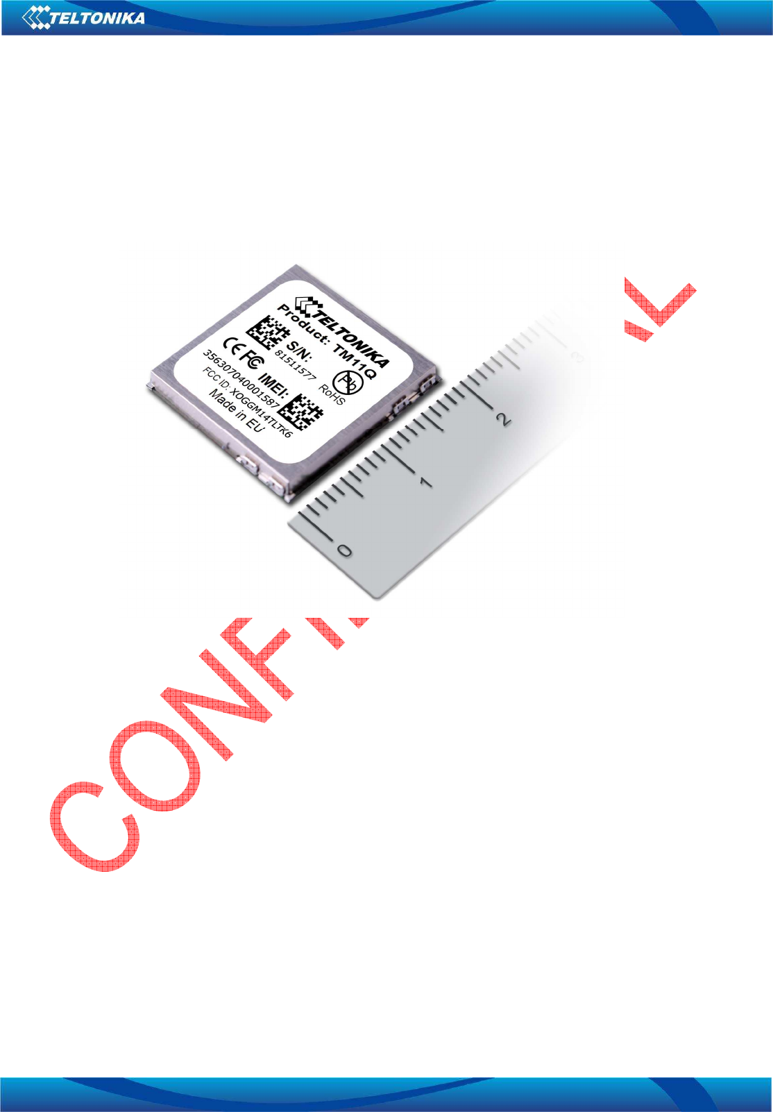
TM11Q is a very small (19x19mm) with BGA type pins, light weight and low power consumption module that
enables digital communications GSM/GPRS networks for machine to machine, user to user or user to
machine wireless applications.
3.1 Certification Requirements
TM11Q GSM/GPRS Data Module is certified by CE approval report and Radio & Telecommunications
Terminal Equipment Directive (R&TTED) report.
Hereby, Teltonika declares that this GSM/GPRS Data Module is in compliance with the essential
requirements and other relevant provisions of Directive 1999/5/EC. The directives that will be followed for
this data module are described below:
3GPP TS 51.010-1 rel.99
Technical Specification Group GSM Radio Access Network and Mobile Station (MS) conformance
specification;
EN 301 489-01 V1.4.1
Electromagnetic compatibility and Radio spectrum Matters (ERM); ElectroMagnetic Compatibility (EMC)
standard for radio equipment and services; Part 1: Common technical requirements;
EN 301 489-07 V1.2.1
Electromagnetic compatibility and Radio spectrum Matters (ERM); ElectroMagnetic Compatibility (EMC)
standard for radio equipment and services; Part 7: Specific conditions for mobile and portable radio and
ancillary equipment of digital cellular radio telecommunications systems (GSM and DCS);
EN 60950-1
Standard for safety of information technology equipment: to protect against excessive current, short circuits
and earth faults in primary circuits protective devices shall be included either as integral parts of the
equipment or as parts of the building installation;
2006/95/EC (Low Voltage Directive)
The Low Voltage Directive (LVD) 73/23/EEC seeks to ensure that electrical equipment within certain
voltage limits both provides a high level of protection for European citizens and enjoys a Single Market in
the European Union.
Requirements for lead-free components are imposed and satisfied.
No natural rubbers, no hygroscopic materials nor materials containing asbestos are employed.
The operative temperature range is from -20 to +85 °C.
NOTE: This equipment has been tested and found to comply with the limits for a Class B digital device,
pursuant to part 15 of the FCC Rules. These limits are designed to provide reasonable protection against
harmful interference in a residential installation. This equipment generates uses and can radiate radio
frequency energy and, if not in-stalled and used in accordance with the instructions, may cause harmful
interference to radio communications. However, there is no guarantee that interference will not occur in a
particular installation. If this equipment does cause harmful interference to radio or television reception,
which can be determined by turning the equipment off and on, the user is encouraged to try to correct the
interference by one or more of the following measures:
- Reorient or relocate the receiving antenna.
- Increase the separation between the equipment and receiver.
- Connect the equipment into an outlet on a circuit different from that to which the receiver is
connected.

8
TM11Q User Manual v1.0
For
7 layers AG
Internal Use Only
Reproduction forbidden without
Teltonika
, UAB written authorization
–
All Rights Reserved
- Consult the dealer or an experienced radio/ TV technician for help.
This equipment is intended to be commercialised in all the countries of the European Union and there is no
commercialisation or operational restrictions in any of the countries.
Hereby, Teltonika JSP declares that this GSM module is in compliance with the essential requirements and
other relevant provisions of Directive 1999/5/EC.
Interference statement:
This device complies with Part 15 of the FCC Rules.
Operation is subject to the following two conditions:
(1) this device may not cause harmful interference, and
(2) this device must accept any interference received, including interference that may cause undesired
operation.
Modification statement:
The FCC requires the user to be notified that any changes or modifications made to this device that are not
expressly approved by a certification authority, may void the user’s authority to operate the equipment.
CAUTION: This device has been evaluated for and shown compliant with the FCC RF exposure limits
under portable exposure conditions (antennas are within 20 cm of a person's body) when installed in
certain specific OEM configurations. This device has also been evaluated and shown compliant with the
FCC RF Exposure limits under mobile exposure conditions (antennas are greater than 20cm from a
person's body).

9
TM11Q User Manual v1.0
For
7 layers AG
Internal Use Only
Reproduction forbidden without
Teltonika
, UAB written authorization
–
All Rights Reserved
4 Product features
The TM1Q GSM/GPRS data module integrates a full-featured Release 99 GSM-GPRS protocol stack,
whose main characteristics are listed in the following. Refer to the PICS/PIXIT documentation for a detailed
description of the stack features. The module main features are:
• Quad band support: GSM 850 MHz, EGSM 900 MHz, DCS 1800 MHz and PCS 1900 MHz;
• Class 4 (33 dBm) for GSM/EGSM bands;
• Class 1 (30 dBm) for DCS/PCS bands;
• All GPRS coding schemes from CS1 to CS4 are supported;
• Encryption algorithms A5/1 for GSM and GPRS are supported;
• CS Data calls are supported in transparent/non transparent mode up to 9.6 kbps;
• Bearer service fax Group 3 Class 2.0 is supported;
• Weight < 3g;
• Dimensions 19mm x 19mm x 3mm.
The GPRS modem is a Class B Mobile Station; this means the data module can be attached to both GPRS
and GSM services, using one service at a time. Network operation modes I to III are supported, with user-
definable preferred service between GSM and EGPRS.
Optionally paging messages for GSM calls can be monitored during GPRS data transfer in not-coordinating
network operation mode NOM II-III.
PBCCH/PCCCH logical channels are supported, as well as CBCH reception. CBCH reception when on
PBCCH is supported.
GPRS multislot 10 is implemented, implying a maximum of 4 slots in DL (reception) and 2 slots in UL
(transmission) and maximum of 5 active channels (slots).
4.1 Supplementary services
The following supplementary services are provided:
• Call Hold/Resume (CH);
• Call Waiting (CW);
• Multi-Party (MTPY);
• Call Forwarding (CF);
• Call Divert;
• Explicit Call Transfer (ECT);
• Call Barring (CB);
• Call Completion to Busy Subscriber (CCBS);
• Advice of Charge (AoC);
• Calling Line Identification Presentation (CLIP);
• Calling Line Identification Restriction (CLIR);
• Connected Line Identification Presentation (COLP);
• Connected Line Identification Restriction (COLR);
• Unstructured Supplementary Services Data (USSD);
• Network Identify and Time Zone (NITZ).

10
TM11Q User Manual v1.0
For
7 layers AG
Internal Use Only
Reproduction forbidden without
Teltonika
, UAB written authorization
–
All Rights Reserved
4.2 SMS
SMS Classes that are supported by TM1Q Data Module are 0, 1, 2 and 3. Mobile-originated and mobile-
terminated SMS are supported. Others SMS features that are implemented in TM1Q Data Module are
reported in the following:
• SMS Cell Broadcast (SMS CB);
• Concatenated SMS;
• Text and PDU mode are supported;
• Reception of SMS during circuit-switched calls;
• Reception of SMS via GSM or GPRS;
• SMS storage customizable and configurable is provided.
4.3 AT-command support
The modem functionalities and services are provided through a rich serial AT-command interface.
Standards of AT commands that are supported on the module are:
• 3GPP TS 27.007;
• 3GPP TS 27.005;
• Proprietary AT commands.
For more details on the commands list and their syntax refer to AT commands Manual.

11
TM11Q User Manual v1.0
For
7 layers AG
Internal Use Only
Reproduction forbidden without
Teltonika
, UAB written authorization
–
All Rights Reserved
5 HW functions
5.1 Audio
5.1.1 Circuit description
The module provides the following audio interface pins:
• Two microphone inputs:
The first microphone balanced input MICP1/MICN1 can be used with additional circuitry to
connect an electret condenser microphone used in the handset mode or in the hands free
mode.
The second microphone input EXT_MIC can be used to directly connect an electret
condenser microphone used in the headset mode.
• Two speaker outputs:
The first speaker output EPPA is a single ended low power audio output which can be used
to directly connect a receiver or an earpiece used in the handset mode or in the headset
mode.
The second speaker output AUOP/AUON is a differential high power audio output which can
be used to directly connect a speaker or a loud speaker used in the ring tones or in the
hands free mode.
• I2S digital audio interface.
• Headset detection input.
The table below shows pins related to the analog audio signals.
PIN
# TM11Q
Signal Name TM11Q
I/O Function Remarks
F7 EPPA O Low power single-
ended analog audio
output
Used in handset or in
headset mode
G8 AUOP O High power
differential analog
audio output
Used in ring tones or in
hands free mode
H8 AUON O High power
differential analog
audio output
Used in ring tones or in
hands free mode
B8 MICP1 I Microphone signal
input, Balanced +
Audio input requires
additional circuitry. If not
used don’t connect it
C8 MICN1 I Microphone signal
input, Balanced - Audio input requires
additional circuitry. If not
used don’t connect it
E8 VMIC O External
microphone power
supply output
For using with MICP1 and
MICN1. If not used don’t
connect it
D8 EXT_MIC I External
microphone single-
ended input
Audio input
F4 HS_DET I Head-set Detection
input Requires special FW. If not
used don’t connect it.

12
TM11Q User Manual v1.0
For
7 layers AG
Internal Use Only
Reproduction forbidden without
Teltonika
, UAB written authorization
–
All Rights Reserved
5.1.1.1 Analog uplink path (microphones inputs)
The TX (uplink) path of the analog audio front-end on the module consists of two microphone circuits.
Two electret condenser microphones can be connected to the two microphone inputs available on the
module. One is balanced inputs MIC1P and MIC1N and other single ended input EXT_MIC. The main
required electrical specifications for the electret condenser microphone are 2.2 kOhm as maximum
output impedance at 1 kHz and 2 V maximum standard operating voltage.
In the transmit section of the chipset audio front-end there is an input multiplexer which selects either
one of the two microphone inputs, MIC1 and EXT_MIC. These two microphone inputs have the same
characteristics: each path is composed by a settable analog gain stage, an analog switching stage, an
anti alias filter stage before the 16 bit ADC converter which provides the audio sample to the sample-
based voiceband processing system. The uplink path of the microphone can be muted.
The microphone supply provided by the module (output pin VMIC) is single-ended but the supply
voltage refers to the local microphone ground and hence the noise in the ground plane, generated
between analog ground and microphone, will be rejected. Using this concept the electret microphone is
supplied by the single ended supply.
A low pass filter is inserted in the supply structure to reject the supply noise.
Since differential microphone input MIC1P/MIC1N is internally biased, a 100nF capacitance is inserted
on each microphone input to reject the DC microphone supply bias provided by the VMIC pin.
Detailed electrical characteristics of audio transmit path and microphone supply can be found in the
section 7.2.3 of this document.
5.1.1.2 Analog downlink path (speaker outputs)
The RX (downlink) path of the analog audio front-end of the module consists of two speaker outputs
available pins:
• The EPPA pin represents a low power single ended audio output available for handset or
headset mode. This pin is directly connected to the output of the single ended audio amplifier of
the chipset.
• The AUON/AUOP pins represent a high power differential audio output, available for hands free
or ringer mode. These two pins are directly connected to the output of the high power differential
audio amplifier of the chipset.
Inside the baseband chipset, the analog audio front end of the two downlink audio paths (speaker
outputs) are both connected to the digital voiceband processing system by a 16 bit DAC. Analog
amplifying stages with an output switch matrix ensure connection to different acoustic transducers.
The high power differential audio amplifier can be used as a voice amplifier for the hands-free
functionality and as a melody player amplifier for ringer functionality (see the next sections). The melody
player could be the Midi synthesizer or the tone generator. In order to minimize the clipping of the audio
signal, the polarization voltage can be adapted to the voltage supply (battery voltage).
Warning: excessive sound pressure from earphones and headphones can cause hearing loss.
Detailed electrical characteristics of the low power single-ended audio receive path and the high power
differential audio receive path can be found in the section 7.2.4 of this document.
13
TM11Q User Manual v1.0
For
7 layers AG
Internal Use Only
Reproduction forbidden without
Teltonika
, UAB written authorization
–
All Rights Reserved
5.1.2 Handset and headset mode
A headset or a handset can be connected directly to the module adapter board to perform a voice call:
Handset:
Handset mode is the normal voiceband functional mode of the data module, completely handled by the
chipset:
• Handset microphone is connected to balanced input pins MICP1/MICN1 with using connection
circuitry (please refer to the TM11Q HW User Manual);
• Handset receiver is directly connected output pin EPPA.
Headset:
The audio path is automatically switched from handset mode to headset mode when a rising edge is
detected by the chipset from the pin G1 (CAP00_EX5IN line). The audio path returns to the handset mode
when the line returns to low level.
If the module is connected to its adapter board, the CAP00_EX5IN line will be connected to the headset
plug connector (switch pin) mounted on the adapter board, so a rising edge will be present on this line at
the insertion of a headset plug in the relative connector.
To enable the headset detection feature, the CAP00_EXIN5 pad must be configured by means of software
setting. The pad can also be configured by means of software settings as to external interrupt input or
GPIO.
PIN
# TM11Q
Signal Name TM11Q
I/O Function Remarks
G1 CAP00_EX5IN
I Headset detection
input Generic digital interfaces
voltage domain.
Output driver class E.
PU/PD class B.
Value at reset: T/PD.
I External interrupt
input
I/O GPIO
This is the audio path used in headset mode:
• Headset microphone is directly connected to input pin EXT_MIC;
• Headset receiver is directly connected to output pin EPPA.
5.1.3 Hands free mode
Hands-free functionality is implemented using appropriate DSP algorithms for voice band handling
(echo canceller and automatic gain control), managed via software. The viva voice operation provides
the possibility to realize a phone call with a loudspeaker and a microphone. This is the audio path used
in hands free mode:
• Handset microphone is connected to balanced input pins MICN 1/MICN1 with using connection
circuitry (please refer to the TM11Q HW User Manual);
• High power loudspeaker is directly connected to output pins AUOP/AUON.
When the hands free mode is enabled, the audio output signal on the EPPA pin is disabled.

14
TM11Q User Manual v1.0
For
7 layers AG
Internal Use Only
Reproduction forbidden without
Teltonika
, UAB written authorization
–
All Rights Reserved
5.1.4 Ringer mode
The data module supports 40 tones polyphonic ring tones. The ringer tones are generated by chipset
built-in generator and then amplified by the internal amplifier before being applied to a loudspeaker
through the pins AUOP/AUON.
Polyphonic ring-tones can be generated by an internal MIDI synthesizer, which runs at 16 or 32 kHz
sample frequency and can sum up to 40 voices at 16 kHz sampling rate.
The synthesizer output is only mono and cannot be mixed with TCH voice path (the two are mutually
exclusive). To perform in-band alerting during TCH with voice path open, only Tone Generator can be
used.
The output samples of the synthesizer are post processed by two modules:
• High Frequency Shelving Filter: This module is implemented as a first order IIR Filter, which is
mainly used for high frequency boost in audio signals. Its transfer function can be controlled by 4
filter coefficients.
• Audio Compressor: The audio compressor is a device for manipulating the dynamic range of
mono or stereo audio signals. The audio compressor can be controlled by 14 configuration
parameters.
Polyphonic standard format supported.
The MIDI driver can play:
• MIDI files conforming to:
General Midi Level 1.0 with file-format 0 and 1;
General Midi Lite 1.0.
• SP-Midi (Scalable Polyphony MIDI) files conforming to:
SP-Midi 1.0.
• i-Melody files conforming to:
i-Melody v.1.2 specifications.
5.1.5 Audio codecs
The following speech codecs are supported in firmware on the DSP:
• GSM Half Rate (TCH/HS);
• GSM Full Rate (TCH/FS);
• GSM Enhanced Full Rate (TCH/EFR);
• 3GPP Adaptive Multi Rate (AMR) (TCH/AFS+TCH/AHS).
5.1.6 Echo canceller and noise reduction
For better handling of speech calls and audio functionalities, the product supports algorithms for echo
cancellation, noise suppression and automatic gain control. Algorithms are configurable by parameters
editable by AT command.
Parameters can be saved in 2 customer profiles.
5.1.7 Digital filters and gains
In order to match compliance to audio test specification, configurable digital filters, digital gain, analog
gain are available on uplink and downlink audio paths. Also side tone gain (feedback from uplink to
downlink path) is configurable. These audio parameters can be changed by dedicated AT command and
saved in 2 customer profiles.
15
TM11Q User Manual v1.0
For
7 layers AG
Internal Use Only
Reproduction forbidden without
Teltonika
, UAB written authorization
–
All Rights Reserved
5.1.8 I2S interface
The module supports the employment of a bidirectional I2S digital audio interface used to interconnect
audio transmission between the chipset and external audio components. The I2S is a 4-wires (I2S
transmit data, I2S receive data, I2S clock, i2S word alignment) interface. The module acts as master: I2S
clock, i2S word alignment signals are outputs for the module and inputs for the external device.
Since all the I2S interface pins provides alternative functionalities by means of software settings, the I2S
interface is available on the data module only if the SPI interface is disabled. The I2S interface pins can
also be configured as GPIO: with this configuration I2S digital audio interface and SPI interface are both
not enabled.
The description of the pins related to the I2S interface is reported in the following table:
PIN
# TM11Q
Signal Name TM11Q
I/O Function Remarks
E3 SSCO_MRST
O SPI sync data
(MOSI) Generic digital interfaces
voltage domain.
Output driver class D.
PU/PD class B.
Value at reset: T.
O I2S word
alignment (WA)
I/O GPIO
E6 SPI_CS
O SPI chip select Generic digital interfaces
voltage domain.
Output driver class D.
PU/PD class B.
Value at reset: T.
O I2S transmit data
(TX)
I/O GPIO
E5 SSCO_CLK
O SPI clock Generic digital interfaces
voltage domain.
Output driver class D.
PU/PD class B.
Value at reset: T.
O I2S clock (CLK)
I/O GPIO
36 SSCO_MTSR
I SPI sync data
(MISO) Generic digital interfaces
voltage domain.
Output driver class D.
PU/PD class B.
Value at reset: T.
I I2S receive data
(RX)
I/O GPIO
The I2S can be configured by means of software settings in two modes:
• PCM mode;
• DAI mode.
Except the supported transmission modality, the main difference between the PCM mode and the DAI
mode is represented by the logical connection (inside the chipset) to the digital audio processing system
integrated in the firmware:
• In PCM mode the interface is logically connected inside the chipset to the voiceband processing
system as the analog audio front end at the input of the sample-based processing part: this
mode provides complete audio processing possibility;
• In DAI mode the interface is logically connected at the end of the sample-based voiceband
processing part as input and output: this mode is used for certification testing of audio and
vocoder functions, connecting the module to a system simulator.

16
TM11Q User Manual v1.0
For
7 layers AG
Internal Use Only
Reproduction forbidden without
Teltonika
, UAB written authorization
–
All Rights Reserved
5.1.8.1 PCM mode
In PCM mode the I2S TX and RX connections are parallel to the Analog front end (please refer to the
TM11Q HW User Manual), so resources available for analog path can be shared:
• Digital filters and digital gains are available in both uplink and downlink direction. AT commands
for audio parameter management can be addressed to this path;
• Ringer tone and service tone are mixed on the TX path when active(downlink);
• The HF algorithm acts on I2S path.
These are the main feature of the I2S interface in PCM mode:
• I2S runs in PCM - short alignment mode (configurable by AT command);
• I2S on module’s side acts as master (CLK and WA signals are generated by the module);
• WA signal always runs at 8 kHz;
• WA toggles high for 1 or 2 CLK cycles of synchronism (configurable), then toggles low for 16
CLK cycles of sample width. So frame length can be 1 + 16 = 17 bits or 2 + 16 = 18 bits;
• CLK frequency depends on frame length so can be 17 x 8 kHz = 136 kHz or 18 x 8 kHz = 144
kHz;
• TX, RX data are 16 bit words with 8 kHz sampling rate, mono. Data are in 2’s complement
notation. MSB is transmitted first;
• When WA toggles high, first synchronism bit is always low. Second synchronism bit (present
only in case of 2 bit long WA configuration) is MSB of the transmitted word (MSB is transmitted
twice in this case);
• TX changes on CLK rising edge, RX changes on CLK falling edge.
5.1.8.2 DAI mode
In DAI mode the I2S TX and RX access the path to RF link in an entry point behind the audio
processing resources, and it is used for certification testing of audio and vocoder functions, connecting
the module to a system simulator.
The DAI mode is reserved for test mode: type approval compliant to ETSI TS 151 010-1 conformance
specification, chapter 30, Speech Teleservices. The DAI interface is compliant to specification 3GPP TS
44.014 with exception of voltage levels, so to connect the module to a test-set supporting DAI (for
example a R&S UPL16 Audio Analyzer), an external level adapter is needed.
The data exchanged on the interface are 13-bit linear PCM at 8 k samples per second, which are
transferred to and from the module on two serial lines at 104 kbit/s (13 bit x 8 kHz = 104 kbit/s). The
clock line, controlled by the module, clocks the data. The reset line (WA), controlled by the system
simulator, resets the speech transcoder, the speech A/D and D/A functions and starts data
transmission.
Four test modalities are supported in DAI mode:
• Normal Mode: This is the normal operational mode (DAI is off). During a voice call the samples
computed by uplink path are written to speech encoder. The samples are copied out of the
speech decoder the downlink path. No sample is written or read form the DAI.
• Vocoder Test: DAI is connected to the vocoder. The audio scheduler reads the sample from the
DAI-Rx register and transfers it to the speech encoder. It reads samples from the speech
decoder and writes the sample to the DAI-Tx register. The microphone signal is looped back to
the loudspeaker (near end speaker will hear a loop).
• Acoustic Test: DAI is connected to the audio front end (microphone and speaker).The audio
scheduler reads the sample from the DAI-Rx register and transfers it to downlink path
(speaker). It reads a voice sample from the uplink path (mic) and writes the sample to the DAI-
Tx register. The speech decoder output is looped back to the encoder input (far end speaker
will hear a loop).
17
TM11Q User Manual v1.0
For
7 layers AG
Internal Use Only
Reproduction forbidden without
Teltonika
, UAB written authorization
–
All Rights Reserved
• Voiceband Test: The output of the speech decoder is copied into the input of the speech
encoder so the downlink signal is looped back to the uplink (far end speaker will hear a loop).
The microphone signal is looped back to the loudspeaker (near end speaker will also hear a
loop). No sample is written or read form the DAI.
5.2 Power management
5.2.1 Battery power supply
The module has to be supplied by a Li-Ion battery or another power supply able to provide a stable
voltage level due to the bursty current consumption profile of the GSM system.
The module support Li-Ion rechargeable battery type, with a 500mAh minimum capacity and 650mAh
typical value. Other type of batteries can be supported in TM1Q with dedicated SW.
Do not connect any power supply at the supply pins if the module is supplied with a battery.
The external supply (or the battery) has to be connected to the following pins of the module:
PIN
# TM11Q
Signal Name TM11Q
I/O Function Remarks
F1, F2, F3 VBAT I Battery Voltage
Supply Input VBAT pins are internally
shorted between them.
B7, C2, F6,
F8, G3, G4,
G5, G6, G7,
H3, H6, H7
GND NA Ground GND pins are internally
shorted between them.
The operating range of VBAT must be between 3.5 V and 4.2 V, with a typical value of 3.8 V. The peak
current value needed by the module could be up to 2.5 A during a GSM burst transmission.
Description Min Typ Max
Supply voltage (VBAT) operating range
3.5 V
3.8 V
4.2 V
VBAT voltage is directly connected to the BaseBand integrated power management unit: all supply
voltages needed are generated on-chip with integrated linear voltage regulators. The input of these linear
voltage regulators is the battery voltage. The external memory and SIM card supply is provided by the
on-chip voltage regulators.
The integrated power management also provides the control state machine for system start up, including
start up with discharged batteries, pre-charging and system reset control.
VBAT voltage is directly connected also to the RF Power Amplifier.
BaseBand voltage regulators can be set by software in different ways. BaseBand part programs them at
startup and every time changes are necessary.
Two hot spots can be considered: the RF Power Amplifier, and the BaseBand. The heat dissipation is
based on the thermal resistance reduction around these two components by using a large number of vias
in those regions.
18
TM11Q User Manual v1.0
For
7 layers AG
Internal Use Only
Reproduction forbidden without
Teltonika
, UAB written authorization
–
All Rights Reserved
5.2.2 Charger interface
For the battery charging functionalities the module is provided with an external circuitry and software.
There are available two charger pins reported below:
PIN
# TM11Q
Signal Name TM11Q
I/O Function Remarks
D7 CS O Charger Select
Output
Integral battery charger
requires additional
schematic and FW
harmonized with current
consumption of module. If
not used don’t connect it
C7 CDT I Charger Detect
input signal Charger Voltage
Measurement Input
In the following figure is reported the schematic diagram related to the charger additional circuit:
Figure 5-2-2: Charger circuit description
The negative pole of the charger must be connected to the GND pins.
Do not connect any battery charger at the VCHARGE input if is not connected any battery to the VBAT
pins: if a battery is not used or the battery charging is not activated the VCHARGE must be unconnected.
In order to not damage the module and the battery is recommended the use of chargers that are
compliant with the characteristics listed in this user manual.
The main features of the battery charger system implemented on the TM11Q data module with the
charger circuitry are listed in the following:
• Charger voltage range goes from 5 to 15 Volts while the charger current must be limited to 500
mA at any load condition;
• The supported battery voltage range goes from 3.1 V to 4.47 V;
• The charger circuitry generates the power on after battery connection or charger connection;

19
TM11Q User Manual v1.0
For
7 layers AG
Internal Use Only
Reproduction forbidden without
Teltonika
, UAB written authorization
–
All Rights Reserved
• The charging is optimized for current adjusted in the AC-DC wall adapter charger;
• Charger detection supported;
• Battery over-voltage detection, battery voltage monitoring;
• Protection against over-voltage integrated on the data module;
• Pre-charging (e.g. for deep discharged batteries);
• Software controlled charging supported.
In an electronic (switched) charger, the charge current is usually constant and defined by the electronics
control in the charger. The shortest charge times can be reached with constant current charger.
The charger circuit can handle the normal AC supply frequency range from 50 to 60 Hz (dedicated SW
must be implemented in the module).
The battery over-voltage detection is implemented for emergency switching off charging if e.g. the
batteries are removed during charging or battery protection. The over-voltage level can be set by a
register bit to 4.47 V.
The battery voltage monitoring function is implemented for system start up and shut down. It delivers the
input signals for the PMU state machine. The shut down feature is implemented as an emergency shut
down. A controlled shut down should be done by software after measuring the battery voltage using the
measurement unit.
The power on reset is released if the battery voltage exceeds typical 2.5 V (2.25 V...2.85 V).
The power on reset starts the LRTC regulator. The system is started by the PMU state machine.
If the batteries are deeply discharged (that means battery voltage is between 0 V and 3.1 V) and the
device is off (or software has not disabled pre-charging) the charger circuits starts pre-charging beginning
when an AC-DC wall adapter is connected to the module. In pre-charging the charge switch is pulsed
with 100 Hz and a duty cycle of 12.5%. That means the average charge current is reduced to avoid
overheating of the charger parts and to gentle charge the deeply discharged batteries. Pre-charging is
hardware controlled and continued as long as the software switches off precharging.
If software is running, it can switch off the pre-charging function. That means the hardware will not start
any charging after an AC-DC wall adapter was connected. The software is always informed when charger
is connected & disconnected, so the charge switch (main controller of the charging process) can be
controlled by software according to the software charge algorithm.
The duty cycle of the charge current never reach 100% so when the software closes the charge switch
(transistor T1 is conducting) it is not closed for 100% of the time but still pulsed with a 100 Hz clock and
its on-time is >99% of a period. The remaining off time is used to check if the AC-DC wall adapter is still
connected since detection is critical when charging switch is closed.
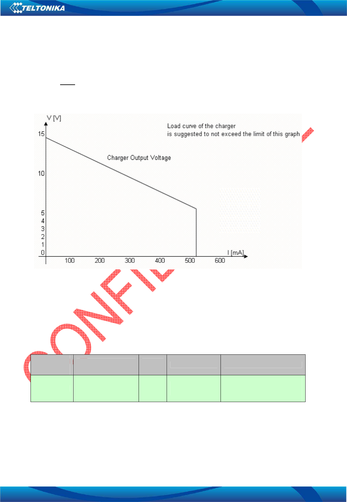
The integrated charging circuit doesn’t have any voltage or current limitation, therefore the charger must
be chosen very carefully: see the below charger specification section.
During the fast charging, that follows the precharging phase, the battery is charged with constant current I
which has to be limited by the charger appropriate selection. This current is monitored by the software
with the aid of the series resistor 0.15 Ohm and by the measuring of the CDT voltage and the battery
voltage. If the charging current I exceeds the limit of 500 mA the charging is stopped to prevent circuit
and battery damages. When the battery voltage reaches the nominal maximum voltage, the charging
enters in the constant voltage phase where the average charging current decreases until the battery in
completely charged.
The charging is enabled only if the module temperature is between the range 0°C to 40°C in order to
satisfy the battery specification. In order to enhance the battery temperature estimation, optionally the
module can use an external NTC temperature sensor in close thermal contact to the battery surface. The
NTC has to be connected using the TBAT pin.
20
TM11Q User Manual v1.0
For
7 layers AG
Internal Use Only
Reproduction forbidden without
Teltonika
, UAB written authorization
–
All Rights Reserved
The charger is detected through the signal CDT when inserted; the minimum threshold at the VCHARGE
input is 4.8V.
The user must use current limited charger. An electronic (switched) charger where the charge current is
usually constant and defined by the electronics control in the charger is usually a good choice.
The charger required characteristics are reported in the following graph.
The limit of 500mA is relative to a battery with minimum 650 mAh of capacitance. The battery can have
greater capacitance but for lower capacitance user has to reduce the charger current.
Selection of very small charge batteries (< 400 mA) is not suggested unless a proper change
(customization) in TELTONIKA SW allows using it.
5.2.3 Real Time Clock supply output
The module provides pin 23 (VRTC) the Real Time Clock supply which is generated by the LRTC linear
regulator of the power management unit integrated in the chipset.
PIN
# TM11Q
Signal Name TM11Q
I/O Function Remarks
H2 VRTC O Real Time Clock
Supply Output
VRTC = 2.0 V (typical) is
enabled if the battery voltage is
inside the valid operating
range.
5.2.4 Power saving
Power saving is a special function that allows the reducing of power consumption during the idle time. If
the clock increases, required power increases too. Therefore a solution for minimizing the power is the
reducing of the master clock frequency when there aren’t activities. In this period the system doesn’t work
21
TM11Q User Manual v1.0
For
7 layers AG
Internal Use Only
Reproduction forbidden without
Teltonika
, UAB written authorization
–
All Rights Reserved
with a clock of 26 MHz (“fast clock”) but with a clock of 32 kHz (RTC clock or “slow clock”). This switching
between 26 MHz and 32 kHz clock is performed by SCCU (Standby Clock Control Unit) integrated in the
baseband chipset.
When the module is registered or attached to a network and a voice or data call is not enabled, it has to
monitor periodically the paging channel of the current base station (paging block reception), as every
mobile station, according to the GSM system specifications and requirements. In between, the module
switches over to a power saving mode, discontinuous reception (DRX).
The module processor core is activated during the paging block reception, so the module switches
automatically its master clock frequency from the 32 kHz used in the power saving mode to the 26 MHz
used in the active mode.
The time period from two paging block receptions is defined by the network. If the module is registered to
a network, the time interval between two paging block receptions can be set from 470.76 ms up to
2118.42 ms.
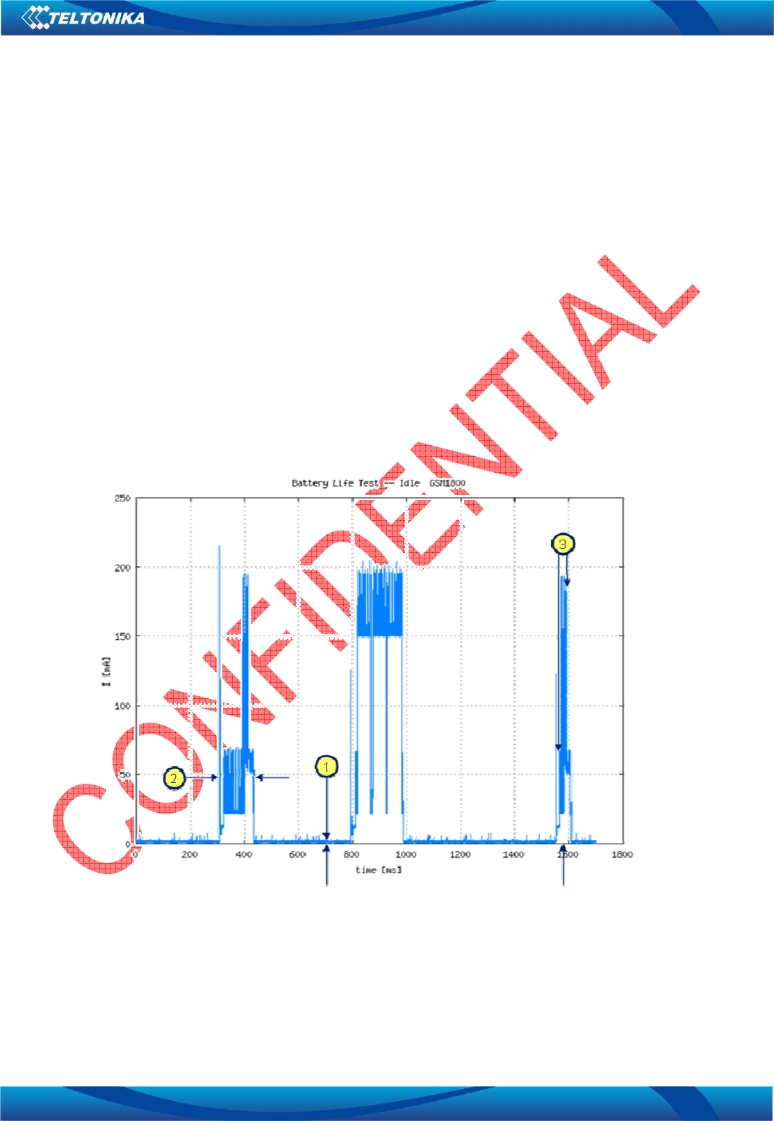
Main priorities of power saving are the following:
1. Reduce base (min) current consumption;
2. Minimize full-speed running periods, minimize power saving on/off switching;
3. Reduce max current consumption.
These points are reported in the following figure:
Figure 5-2-2: Module current consumption profile in GSM idle (DRX-5) with power saving priorities highlighted
More details related to the power saving and the serial port are described in the document
TM11Q_HW_User_Manual.
22
TM11Q User Manual v1.0
For
7 layers AG
Internal Use Only
Reproduction forbidden without
Teltonika
, UAB written authorization
–
All Rights Reserved
This functionality can be disabled by the user through an AT command (more details on the document
TM11Q_AT_Commands_Manual_8MB).
5.2.5 Current consumptions
Current consumptions of the module are reported in the following table:
Mode Average Current
Consumption Note
Power Off Mode < 90 µA Module supplied but
Switched Off
2G (GSM) Idle Mode @ DRX = 2 < 2 mA
2G (GSM) Talk Mode @ 850 / 900 MHz, PCL =
5 (P = 33dBm) < 300 mA
2G (GSM) Talk Mode @ 1800 / 1900 MHz,
PCL = 0 (P = 30dBm) < 220 mA
2.5G (GPRS) attach mode @ DRX = 2 < 1,6 mA
2.5G (GPRS 2+1) TBF mode @ 850 / 900
MHz, PCL = 5 (P = 33dBm) < 250 mA
2.5G (GPRS 2+2) TBF mode @ 850 / 900
MHz, PCL = 5 (P = 33dBm) < 400 mA
2.5G (GPRS 2+1) TBF mode @ 1800 / 1900
MHz, PCL = 0 (P = 30dBm) < 250 mA
2.5G (GPRS 2+2) TBF mode @ 1800 / 1900
MHz, PCL = 0 (P = 30dBm) < 350 mA
Note: The current consumption of the module depends on network condition in all the listed modes
except the power off mode and the airplane mode. The listed current consumption values are referred to
the average current consumption of the whole module, with the module supplied by a 3.8V voltage rail.
23
TM11Q User Manual v1.0
For
7 layers AG
Internal Use Only
Reproduction forbidden without
Teltonika
, UAB written authorization
–
All Rights Reserved
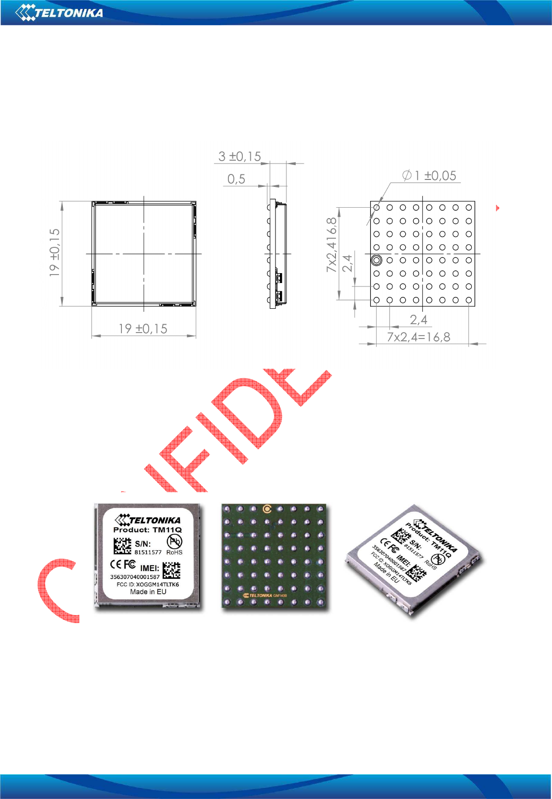
5.3 Mechanical characteristics
The mechanical dimensions of the data module with shields mounted are: 19 mm x 19 mm x 3 mm.
Figure 5-3-1: TM11Q module
The weight is less than 3 g.
No natural rubbers, no hygroscopic materials nor materials containing asbestos are employed.
Figure 5-3-2: TM11Q module
24
TM11Q User Manual v1.0
For
7 layers AG
Internal Use Only
Reproduction forbidden without
Teltonika
, UAB written authorization
–
All Rights Reserved
6 Module interfaces
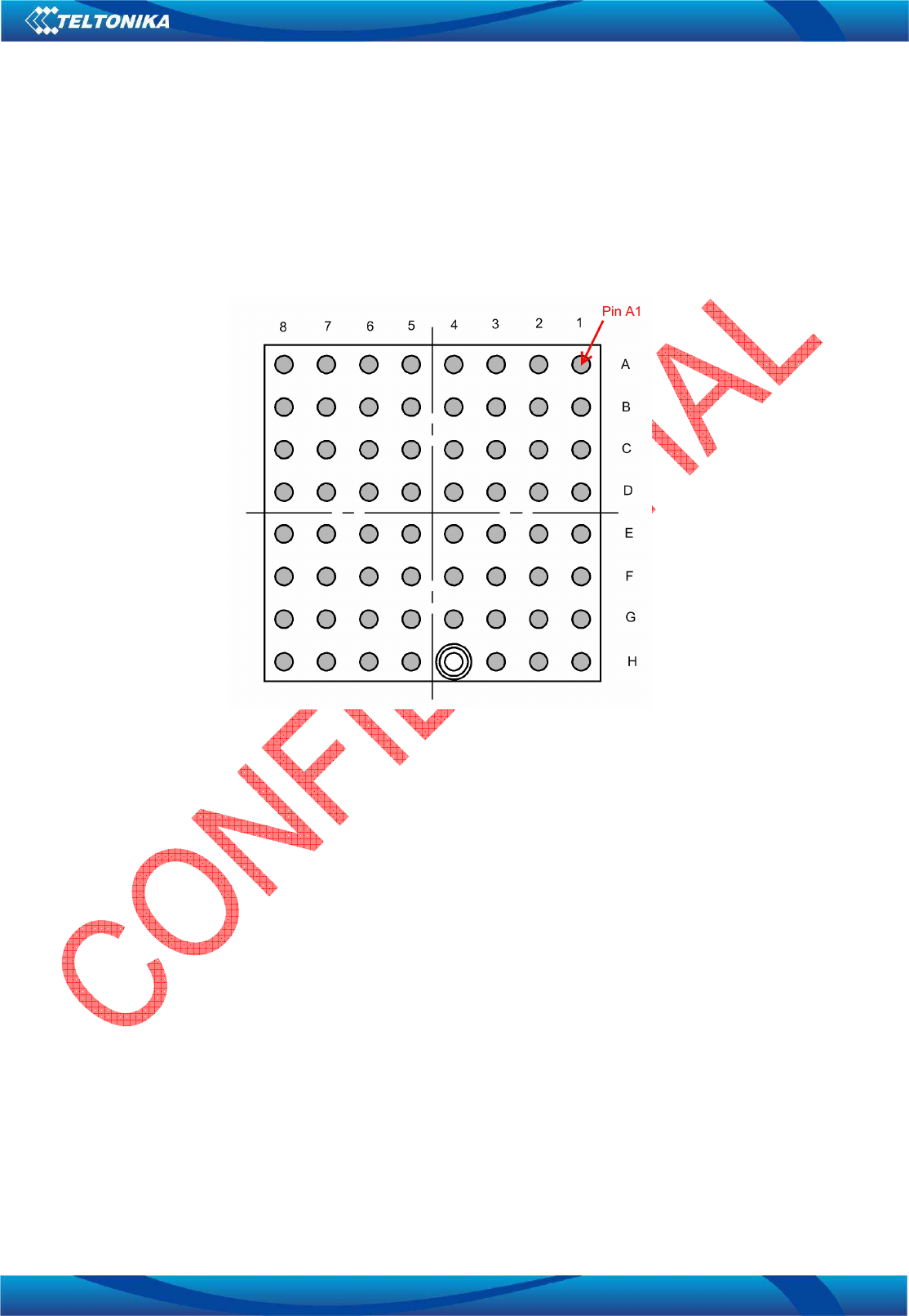
6.1 Pins overview
The TM11Q is equipped with 63 BGA-type pads to connect the module to the external application: the
module can be soldered to customer PCB.
Figure 6-1: Module BGA pins
25
TM11Q User Manual v1.0
For
7 layers AG
Internal Use Only
Reproduction forbidden without
Teltonika
, UAB written authorization
–
All Rights Reserved
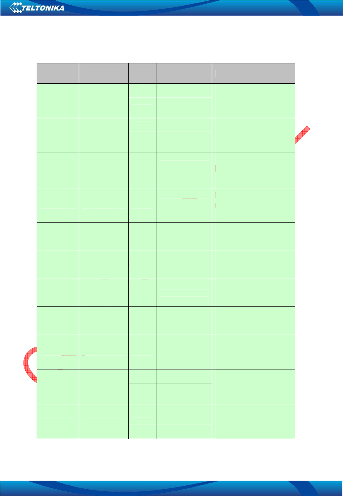
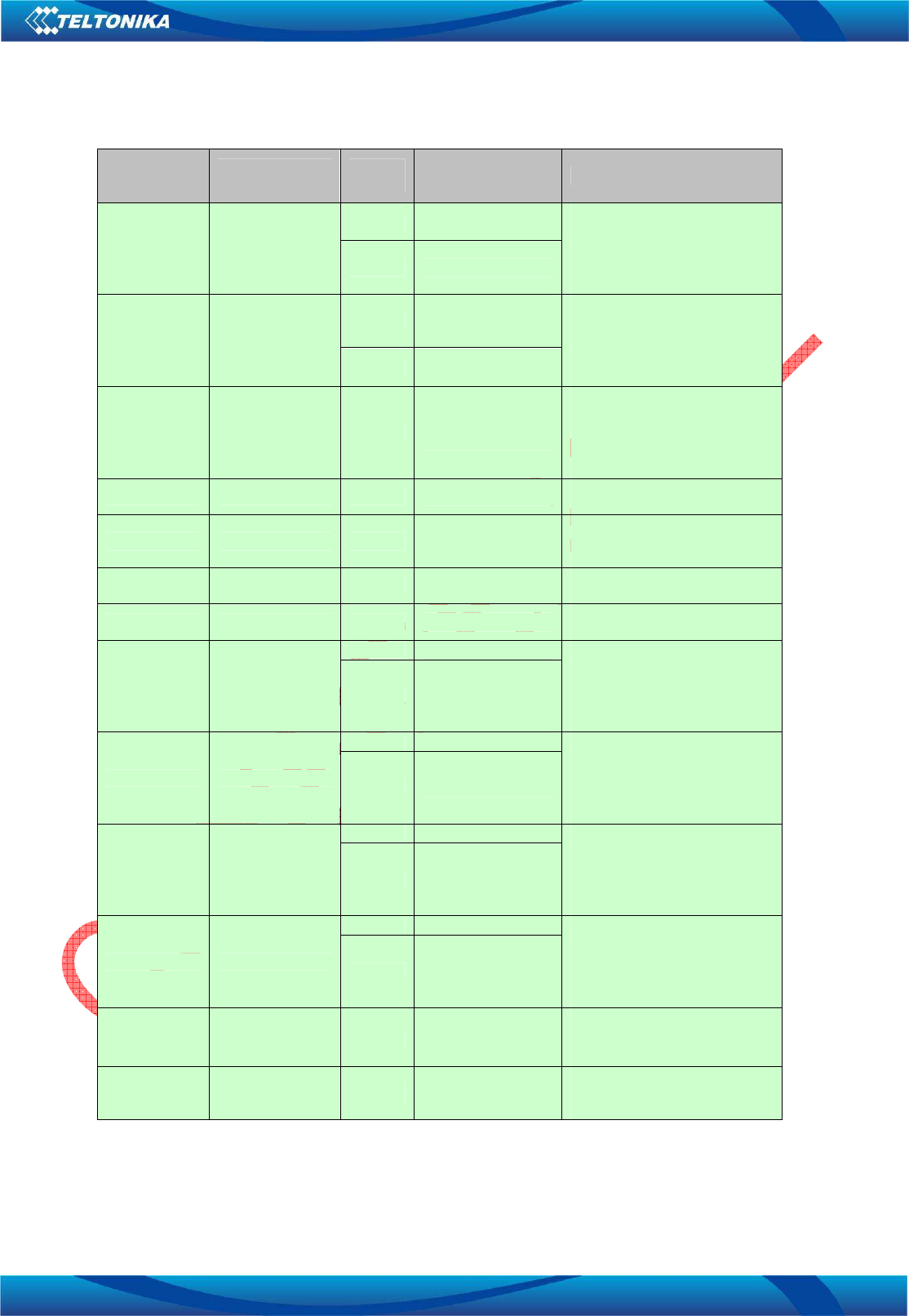
The description of all the BGA pins is reported in the following table:
PIN
# TM11Q
Signal Name TM11Q
I/O Function Remarks
A1 RTSn
O ASC ready to send
(CTS in V.24 spec) Generic digital interfaces
voltage domain.
Output driver class F.
PU/PD class C.
Value at reset: T/PU.
I/O GPIO
A2 CTSn
I ASC clear to send
(RTS in V.24 spec.) Generic digital interfaces
voltage domain.
Output driver class C.
PU/PD class B.
Value at reset: T/PD.
I/O GPIO
A3 TXD O ASC transmitted
data (RX in V.24
spec)
Generic digital interfaces
voltage domain.
Output driver class E.
PU/PD class C.
Value at reset: T.
A4 RXD I ASC received data
(TX in V.24 spec)
Generic digital interfaces
voltage domain.
Output driver class E.
PU/PD class C.
Value at reset: T.
A5 SIM_CLK O SIM clock
SIM interface voltage domain.
Output driver class E.
PU/PD class B.
Value at reset: L.
A6 SIM_IO I/O SIM data
SIM interface voltage domain.
Output driver class E.
PU/PD class B.
Value at reset: OD/L.
A7 VSIM O SIM supply output
VSIM = 1.80 V typical if SIM
card = 1.8V type or
VSIM = 2.85 V typical
if SIM card = 3.0V type
A8 SIM_RST O SIM reset
SIM interface voltage domain.
Output driver class E.
PU/PD class B.
Value at reset: L.
B1 PWR_ON I Power-on input
Generic digital interfaces
voltage domain.
Output driver class F.
PU/PD class A.
Value at reset: T/PD.
B2 DSR
O ASC data set ready
(DSR in V.24 spec.) Generic digital interfaces
voltage domain.
Output driver class B slow.
PU/PD class A.
Value at reset: T/PU.
I/O GPIO
B3 DTR
I ASC data terminal
ready (DTR in V.24
spec.)
Generic digital interfaces
voltage domain.
Output driver class B.
PU/PD class B.
Value at reset: T/PD.
I/O GPIO
26
TM11Q User Manual v1.0
For
7 layers AG
Internal Use Only
Reproduction forbidden without
Teltonika
, UAB written authorization
–
All Rights Reserved
PIN
# TM11Q
Signal Name TM11Q
I/O Function Remarks
B4 RI
O ASC ring indicator
(RI in V.24 spec.)
Generic digital interfaces
voltage domain.
Output driver class D.
PU/PD class B.
Value at reset: T/PD.
I/O GPIO
B5 DCD
O ASC data carrier
detect (DCD in
V.24 spec)
Generic digital interfaces
voltage domain.
Output driver class D.
PU/PD class B.
Value at reset: T/PD.
I/O GPIO
B6 ACK_ON O RESET signal
output
Generic digital interfaces
voltage domain.
Output driver class D.
PU/PD class B.
Value at reset: T/PD.
B7 GND NA Ground GND pins are internally
shorted between them.
B8 MICP1 I Microphone signal
input, Balanced +
Audio input requires additional
circuitry. If not used don’t
connect it
C1 RESETn I External reset input External reset signal voltage
domain.
C2 GND NA Ground GND pins are internally
shorted between them.
C3 KEYIN0
I/O GPIO Generic digital interfaces
voltage domain.
Output driver class F.
PU/PD class B.
Value at reset: T.
I Keypad Input 0
C4 KEYIN1
I/O GPIO Generic digital interfaces
voltage domain.
Output driver class F.
PU/PD class B.
Value at reset: T.
I Keypad Input 1
C5 KEYIN2
I Keypad Input 2 Generic digital interfaces
voltage domain.
Output driver class F.
PU/PD class B.
Value at reset: T.
I/O GPIO
C6 KEYIN3
I Keypad Input 3 Generic digital interfaces
voltage domain.
Output driver class F.
PU/PD class B.
Value at reset: T.
I/O GPIO
C7 CDT I Charger Detect
Input Signal
Integral battery charger
requires additional
schematic.
C8 MICN1 I Microphone signal
input, Balanced - Audio input requires additional
circuitry. If not used don’t
connect it

27
TM11Q User Manual v1.0
For
7 layers AG
Internal Use Only
Reproduction forbidden without
Teltonika
, UAB written authorization
–
All Rights Reserved
PIN
# TM11Q
Signal Name TM11Q
I/O Function Remarks
D1 KEYOUT0
I/O GPIO Generic digital interfaces
voltage domain.
Output driver class F.
PU/PD class B.
Value at reset: T.
O Keypad Output 0
D2 KEYOUT1
I/O GPIO Generic digital interfaces
voltage domain.
Output driver class F.
PU/PD class B.
Value at reset: T.
O Keypad Output 1
D3 KEYOUT2
I/O GPIO Generic digital interfaces
voltage domain.
Output driver class F.
PU/PD class B.
Value at reset: T.
O Keypad Output 2
D4 KEYOUT3
I/O GPIO Generic digital interfaces
voltage domain.
Output driver class F.
PU/PD class B.
Value at reset: T.
O Keypad Output 3
D5 KEYOUT4
I/O GPIO Generic digital interfaces
voltage domain.
Output driver class F.
PU/PD class B.
Value at reset: T.
O Keypad Output 4
D6 KEYOUT5
I/O GPIO Generic digital interfaces
voltage domain.
Output driver class F.
PU/PD class B.
Value at reset: T.
O Keypad Output 5
D7 CS O
Charger Select
Output
Integral battery charger
requires additional
schematic.
D8 EXT_MIC I External
microphone single-
ended input
Audio input
E1 SDA
I/O I2C bus data line I2C interface voltage domain.
Fixed open drain.
External pull-up required.
Value at reset: T/OD.
I/O GPIO
E2 SCL
O I2C bus clock line I2C interface voltage domain.
Fixed open drain.
External pull-up required.
Value at reset: T/OD.
I/O GPIO
E3 SSCO_MRST
O SPI sync data
(MOSI) Generic digital interfaces
voltage domain.
Output driver class D.
PU/PD class B.
Value at reset: T.
O I2S word alignment
I/O GPIO
28
TM11Q User Manual v1.0
For
7 layers AG
Internal Use Only
Reproduction forbidden without
Teltonika
, UAB written authorization
–
All Rights Reserved
PIN
# TM11Q
Signal Name TM11Q
I/O Function Remarks
E4 SSCO_MTSR
I SPI sync data
(MISO) Generic digital interfaces
voltage domain.
Output driver class D.
PU/PD class B.
Value at reset: T.
I I2S receive data
I/O GPIO
E5 SSCO_CLK
O SPI clock Generic digital interfaces
voltage domain.
Output driver class D.
PU/PD class B.
Value at reset: T.
O I2S clock
I/O GPIO
E6 SPI_CS
O SPI chip select Generic digital interfaces
voltage domain.
Output driver class D.
PU/PD class B.
Value at reset: T.
O I2S transmit data
I/O GPIO
E7 TBAT I External Battery
Temperature
Sensor Input
Generic digital interfaces
voltage domain.
E8 VMIC O External
microphone power
supply output
For using with MICP1 and
MICN1. If not used don’t
connect it
F1 VBAT I Battery Voltage
Supply Input VBAT pins are internally
shorted between them.
F2 VBAT I Battery Voltage
Supply Input VBAT pins are internally
shorted between them.
F3 VBAT I Battery Voltage
Supply Input VBAT pins are internally
shorted between them.
F4 HS_DET I Head-set Detection
input Requires special FW. If not
used don’t connect it.
F5 ADC1 I Analog-to-Digital
Converter input Resolution: 12 bits
Voltage span: 0V-1.92V
F6 GND NA Ground GND pins are internally
shorted between them.
F7 EPPA O Low power single-
ended analog audio
output
Used in handset or in headset
mode
F8 GND NA Ground GND pins are internally
shorted between them.
G1 CAP00_EX5IN
I Headset detection
input Generic digital interfaces
voltage domain.
Output driver class E.
PU/PD class B.
Value at reset: T/PD.
I External interrupt
input
I/O GPIO
G3 GND NA Ground GND pins are internally
shorted between them.
G4 GND NA Ground GND pins are internally
shorted between them.
G5 GND NA Ground GND pins are internally
shorted between them.
29
TM11Q User Manual v1.0
For
7 layers AG
Internal Use Only
Reproduction forbidden without
Teltonika
, UAB written authorization
–
All Rights Reserved
PIN
# TM11Q
Signal Name TM11Q
I/O Function Remarks
G6 GND NA Ground GND pins are internally
shorted between them.
G7 GND NA Ground GND pins are internally
shorted between them.
G8 AUOP O
High power
differential analog
audio output ,
positive +
Used in ring tones or in hands
free mode
H1 RES1 NA Reserved pin Not connected
H2 VRTC O Real Time Clock
Supply Output
VRTC = 2.0 V (typical) is
enabled if the battery voltage
is inside the valid operating
range.
H3 GND NA Ground GND pins are internally
shorted between them.
H4 ANT_C I/O Calibration Test
Point Don’t connect it
H5 ANT I/O RF antenna 50Ω nominal impedance
H6 GND NA Ground GND pins are internally
shorted between them.
H7 GND NA Ground GND pins are internally
shorted between them.
H8 AUON O
High power
differential analog
audio output,
negative -
Used in ring tones or in hands
free mode
Several pins are able to provide more then one function: up to three functionalities can be available on
the same pin by means of software setting. In the column “Function” of the previous table is the reported
the description of the available functionalities on the relative pin and in the column “TM1Q I/O” of the
previous table is reported the signal direction from the module point of view of the relative pin
functionality.
In the column “Remarks” of the previous table are reported some additional information regarding the
type of the pin, the voltage domain, the output driver class, the pull-up and pull-down class, the value at
reset.
The pins can be classified in different types, with different characteristics and voltage domains:
• Supply/power pins:
o Battery supply input
o Charger input
o SIM supply output
o Real Time Clock supply output
• Digital pins:
o Generic digital interfaces
o I2C interface
o SIM interface
o RESETn signal
• Audio pins:
o Microphones bias and reference input
o Low power single-ended analog audio output
o High power differential analog audio output

30
TM11Q User Manual v1.0
For
7 layers AG
Internal Use Only
Reproduction forbidden without
Teltonika
, UAB written authorization
–
All Rights Reserved
• ADC pin
• RF antenna pin
Each digital pin has different electrical characteristics as output driver, so there is this classification:
• output driver class B slow
• output driver class B
• output driver class C
• output driver class D
• output driver class E
• output driver class F
Each digital pin has different pull-up and pull-down characteristics, so there is this classification:
• pull-up / pull-down class A
• pull-up / pull-down class B
• pull-up / pull-down class C
The detailed description of the electrical characteristics of all the different pin types can be found in the
section 7 of this document.
During the power-on and power-off sequence or whenever no proper operation of the outputs can be
guaranteed, the digital pins of the module are set to tristate, or are in a proper reset configuration if the
module is in the reset state (see the sections 6.2, 0, 6.4 of this document).
Each digital pin has different value during the reset state of the module, briefly summarized in the column
“Remarks” of the previous table with the following acronyms:
• T = Tristate (output driver disabled)
• PU = Pull Up
• PD = Pull Down
• OD = Open Drain
• L = Low level
• H = High level
If the module is soldered on a customized board, special care must be taken on the layout design of the
board for the pads extension, which should be extended on outer side to increase solder paste volume
and allow soldering on board plated edge.
Note: If a pin is not used, it can be left unconnected: it will be configured by software to a fixed logic level
to minimize the power consumption.
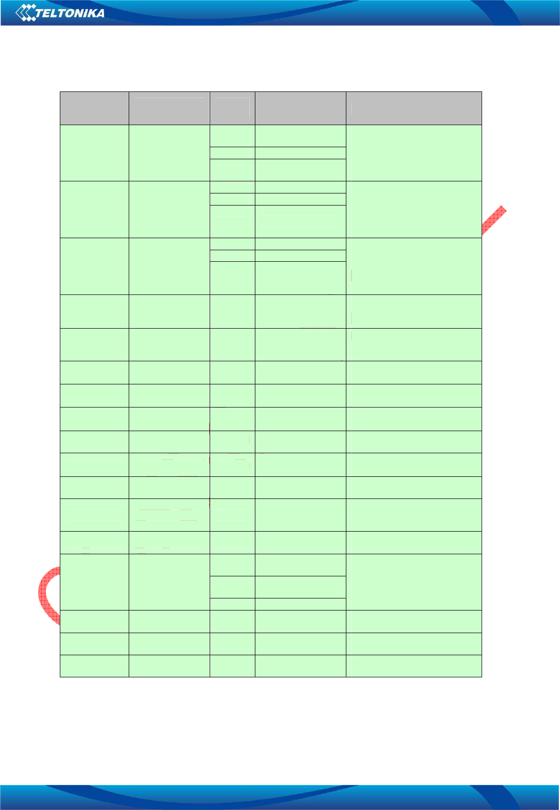
6.2 Module power on
The power on sequence of the module is initiated in one of four ways:
• Connection of a battery with a valid voltage
• Falling edge on the pin B1 (PWR_ON signal)
• RTC alarm
• Connection of a charger with a valid voltage
When a battery supply is connected to the VBAT pins a battery supervision circuit controls the
subsequent activation of the power up state machines: the module is switched-on if the battery is
connected for the first time and the voltage rises up to the valid limit of operation (VBAT > 3.16 V). This is
done to allow the battery management software to detect when the battery has been exchanged or re-
inserted. This information is used to reset timers used for battery capacity estimation in some estimation
concepts, since these are no longer valid if a new battery is inserted.

31
TM11Q User Manual v1.0
For
7 layers AG
Internal Use Only
Reproduction forbidden without
Teltonika
, UAB written authorization
–
All Rights Reserved
The module can be switched-on using the pin B1(PWR_ON signal). The voltage on this pin is pulled to
the high level on the module. The power-on sequence starts when a falling edge occurs on the PWR_ON
signal. This pin can be connected with the ON push button to ground: when the button is pressed, the
signal is shorted to ground.
PIN
# TM11Q
Signal Name TM11Q
I/O Function Remarks
B1 PWR_ON I Power-on input
Generic digital interfaces
voltage domain.
Output driver class F.
PU/PD class A.
Value at reset: T/PD.
The module can be switched-on by the RTC alarm, when Real Time Clock system reaches a pre-defined
scheduled time. The RTC system will then initiate the boot sequence by indicating to the power
management unit to turn on power. Also included in this setup is an interrupt signal from the RTC block to
indicate to the baseband processor, that a RTC event has occurred.
The module can be switched-on by a charger: if the power management unit detects that a charger is
connected to the module, it turns on power and the module is switched on in a charge only mode.
In order to avoid an excessive drop on the battery voltage caused by in-rush current during system
power-on, possibly leading to system instability and “hick-ups”, a staggered turn-on approach for the
regulators is implemented. The regulators are turned on in a well defined sequence, thus spreading the
in-rush current transients over time.
If a valid battery voltage is connected to VBAT pins, before the detection of a start-up event, most input-
output pads of the baseband chipset are locked in tristate. The power down tristate function isolates the
outputs of the module from its environment, whenever no proper operation of the outputs can be
guaranteed. As shown in the power-on sequence figure, the tristate function is controlled by the
baseband signals RESET_BB_N and PM_INT: the pads are locked in tristate during the first power-on
sequence phases. The tristate function ensures that the chip is isolated from the board but, depending on
the pull-up or pull-down controls, it may not result necessarily in a Hi-Z state.
Then, during the power-on sequence, the baseband core is held in reset state before enabling the input-
output pads, to avoid uncontrollable output signals during power-on. Inside baseband chipset the reset
logic is part of the RTC supply domain which is always powered up. This allows to power up the
baseband core regulator and waits for the core to reach reset state before powering up the I/O supply
regulators.
The reset state of all the module input-output pads is reported in the pins description table (in the column
“Remarks”) reported in the section 6.1 of this document.
The complete power-on sequence of the module is shown in the following figure:
32
TM11Q User Manual v1.0
For
7 layers AG
Internal Use Only
Reproduction forbidden without
Teltonika
, UAB written authorization
–
All Rights Reserved
Figure 6-2-1: Power on sequence
The following table shows the complete details of the power up timing including the delays between each
step:
Sequence Function Typical time
for activation of
next sequence step
Cumulative typical time
from EGV start-up
event detection
0 Battery Insertion
1 EGV start-up event detection 20.48 ms 0.00 ms
2 Bandgap circuit activated 1.28 ms 20.48 ms
3 LRFXO activated 0.16 ms 21.76 ms
4 LD1 activated 0.64 ms 21.92 ms
5 LMEM activated 0.16 ms 22.56 ms
6 LIO activated 1.28 ms 22.72 ms
7 PM_INT low 20.48 ms 24.00 ms
8 RESET_BB_N released 44.48 ms
33
TM11Q User Manual v1.0
For
7 layers AG
Internal Use Only
Reproduction forbidden without
Teltonika
, UAB written authorization
–
All Rights Reserved
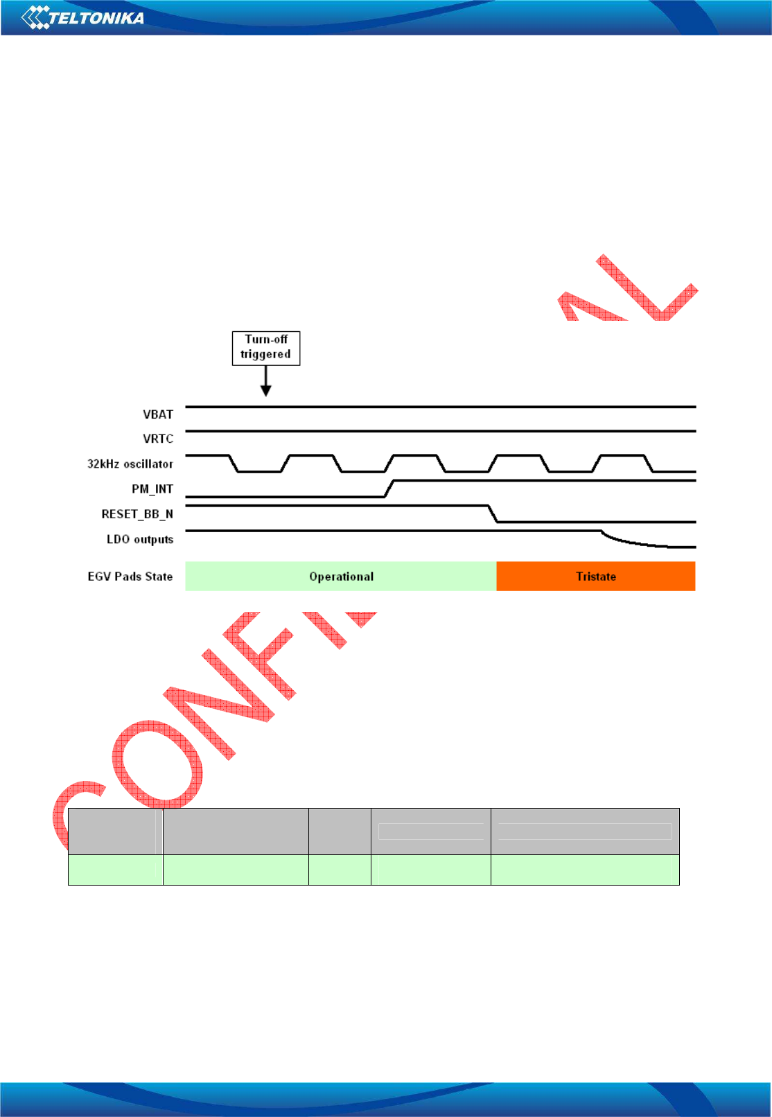
6.3 Module power off
The module can be switched-off by the user through the AT command AT+CPWROFF. The other way to
switch off the module is to hold the PWR_ON signal at low level at least 2-3 sec. An undervoltage
shutdown can be forced by the controller if the battery voltage goes out of the valid limit of operation.
After a turn-off event has been triggered the signal PM_INT is set high and after one clock cycle
RESET_BB_N is set low. This forces the digital pins to tristate mode. After one further counters cycle all
power supplies except LRTC are turned off.
The complete power-off sequence of the module is shown in the following figure:
Figure 6-3-1: Power off sequence
6.4 Module reset
To reset the module the pin C1 (RESETn) must be used: this pin performs an external reset, also called
hardware reset. Driving the RESETn pin low causes an asynchronous reset of the entire device except
for the Real Time Clock block (RTC). The device then enters its power-on reset sequence.
PIN
# TM11Q
Signal Name TM11Q
I/O Function Remarks
C1 RESETn I External reset
input External reset signal voltage
domain.
If the module is connected to its adapter board and then to its mother board, the RESETn will be
connected to the reset push button mounted on the mother board: when the button is pressed, the signal
is shorted to ground and the module reset is performed.
34
TM11Q User Manual v1.0
For
7 layers AG
Internal Use Only
Reproduction forbidden without
Teltonika
, UAB written authorization
–
All Rights Reserved
6.5 RF antenna interface
The BGA-type pad H5 (ANT signal) has an impedance of 50Ω and provides the RF antenna interface.
The pads close to the ANT pin (pads G3, G4, G5, G6, H3 and H6) are ground pads and must be used to
provide the connection of the RF antenna to the grounding plane.
PIN
# TM1Q
Signal Name TM1Q
I/O Function Remarks
H5 ANT I/O RF antenna 50Ω nominal impedance
If the module is soldered on its adapter board, a connection to an SMA connector mounted on the
adapter board is provided to directly connect an antenna with an SMA connector.
If the module is soldered on a customized board, special care must be taken on the layout design for the
RF antenna pad which needs to be designed for 50 Ω impedance.
6.6 SIM interface
A SIM card interface is provided on the pins of the module: the high-speed SIM/ME interface is
implemented as well as the automatic detection of the required SIM supporting voltage.
Both 1.8 V and 3 V SIM type will be supported (1.8 V and 3 V ME); activation and deactivation with
automatic voltage switch from 1.8 V to 3 V are implemented, according to ISO-IEC 78-16-e
Specifications. The SIM driver supports the PPS (Protocol and Parameter Selection) procedure for baud-
rate selection, according to the values proposed by the SIM Card. Clock stop is supported at both high
and low level.
The description of the pins related to the SIM interface is reported in the following table:
PIN
# TM11Q
Signal Name TM11Q
I/O Function Remarks
A5 SIM_CLK O SIM clock
SIM interface voltage domain.
Output driver class E.
PU/PD class B.
Value at reset: L.
A6 SIM_IO I/O SIM data
SIM interface voltage domain.
Output driver class E.
PU/PD class B.
Value at reset: OD/L.
A7 VSIM O SIM supply output
VSIM = 1.80 V typical if SIM
card = 1.8V type or
VSIM = 2.85 V typical
if SIM card = 3.0V type
A8 SIM_RST O SIM reset
SIM interface voltage domain.
Output driver class E.
PU/PD class B.
Value at reset: L.

35
TM11Q User Manual v1.0
For
7 layers AG
Internal Use Only
Reproduction forbidden without
Teltonika
, UAB written authorization
–
All Rights Reserved
6.6.1 SIM functionality
Among SIM functionalities, the following services of the SIM are supported:
• Abbreviated Dialing Numbers (ADN);
• Fixed Dialing Numbers (FDN);
• Last Dialed Numbers (LDN);
• Service Dialing Numbers (SDN);
• ME Personalization (SIM Lock).
ME Personalization handling is a mechanism to tie the ME operation to one specific SIM card or to a
limited range of SIM cards from a given Network Operator or Service Provider. The ME will only accept
the SIM if there is a positive match between the personalization code group(s) stored in the ME and the
code group(s) belonging to the inserted SIM.
The SIM Lock feature supported by TM11Q module enables ME personalization through the following
personalization categories:
• Network lock;
• Network subset lock;
• Service provider lock;
• Corporate lock;
• Operator lock.
SIM Toolkit R97 is supported.
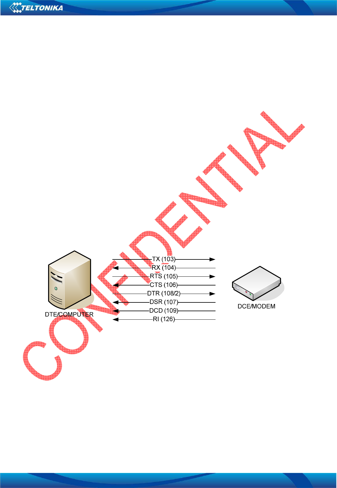
36
TM11Q User Manual v1.0
For
7 layers AG
Internal Use Only
Reproduction forbidden without
Teltonika
, UAB written authorization
–
All Rights Reserved
6.7 Asynchronous serial interface (ASC)
The asynchronous serial interface (ASC) relies on the Asynchronous Serial Controller hardware block
provided by the baseband core.
ASC features are:
• Complete 9-pin serial port in compliance with the ITU V.24 specifications [E.1] (i.e. a complete
RS-232 low voltage interface with hardware flow control is available);
• The maximum data rate is 921600 bps for software download;
• Intermediate data rates can be 2400, 4800, 9600, 19200, 38400, 57600, 115200, 230400,
460800 bps with No/Even/Odd parity, 7 or 8 bit frame length;
• Power saving CTS indication available at the interface (see [I.2]).
Software services available at ASC:
• AT interface in compliance with GSM 27.007 [E.2]: the default speed for the AT interface is
115200 bps, the maximum speed is 230400 bps (see [I.1]);
• MUX protocol available in compliance with GMS 27.010 [E.3];
• Interface can be configured to access this port for customer specific usage by AT commands.
The serial port is limited to 921600 bps due to the FTDI level translator (serial to USB converter) of the
motherboard.
A more detailed description regarding software services and serial port behavior of the module are
provided by the Teltonika documents: TM11Q_AT_Commands_Manual_8MB and
TM1Q_HW_Manual_1.0.
This is the ITU V.24 signals naming convention [E.1]: the module is a Data Communication Equipment
(DCE), which is a modem; the external host processor or the PC is the Data Terminal Equipment (DTE).
Figure 6-7-1: DTE-DCE RS232 interface
ITU V.24 conventional directions are in the previous figure like circuits numbers; please note that the
hardware names of the module pins do not necessary reveal the ITU V.24 functionality.
To download the code, only the two data lines (TXD and RXD) can be used. The other lines (CTS, RTS,
DSR, RI, DCD and DTR) can be configured as GPIO.

37
TM11Q User Manual v1.0
For
7 layers AG
Internal Use Only
Reproduction forbidden without
Teltonika
, UAB written authorization
–
All Rights Reserved
The description of the pins related to ASC interface is reported in the following table:
PIN
# TM11Q
Signal Name TM11Q
I/O Function Remarks
A1 RTSn
O ASC ready to send
(CTS in V.24 spec) Generic digital interfaces
voltage domain.
Output driver class F.
PU/PD class C.
Value at reset: T/PU.
I/O GPIO
A2 CTSn
I ASC clear to send
(RTS in V.24 spec.) Generic digital interfaces
voltage domain.
Output driver class C.
PU/PD class B.
Value at reset: T/PD.
I/O GPIO
A3 TXD O ASC transmitted
data (RX in V.24
spec)
Generic digital interfaces
voltage domain.
Output driver class E.
PU/PD class C.
Value at reset: T.
A4 RXD I ASC received data
(TX in V.24 spec)
Generic digital interfaces
voltage domain.
Output driver class E.
PU/PD class C.
Value at reset: T.
B2 DSR
O ASC data set ready
(DSR in V.24 spec.) Generic digital interfaces
voltage domain.
Output driver class B slow.
PU/PD class A.
Value at reset: T/PU.
I/O GPIO
B3 DTR
I ASC data terminal
ready (DTR in V.24
spec.)
Generic digital interfaces
voltage domain.
Output driver class B.
PU/PD class B.
Value at reset: T/PD.
I/O GPIO
B4 RI
O ASC ring indicator
(RI in V.24 spec.)
Generic digital interfaces
voltage domain.
Output driver class D.
PU/PD class B.
Value at reset: T/PD.
I/O GPIO
B5 DCD O ASC data carrier
detect (DCD in
V.24 spec)
Generic digital interfaces
voltage domain.
Output driver class D.
PU/PD class B.
Value at reset: T/PD.
6.7.1 MUX protocol
The module has a software layer with MUX functionality, GSM 07.10 multiplexer protocol. It is a data link
protocol (layer 2 of OSI model) which uses HDLC-like framing and operates between the module (DCE)
and the application processor (DTE). It allows a number of simultaneous sessions over the physical link,
the UART. Each session consists of a stream of bytes transferring various kinds of data like SMS, CBS,
GPRS, AT commands in general. This permits, for example, SMS to be transferred to the DTE when a
data connection is in progress.
The MUX is implemented in the basic option.
38
TM11Q User Manual v1.0
For
7 layers AG
Internal Use Only
Reproduction forbidden without
Teltonika
, UAB written authorization
–
All Rights Reserved
6.8 Synchronous serial interface (SPI)
The module provides on the pins a synchronous SPI-compatible serial interface implemented with the
synchronous serial controller hardware block of the baseband. The SPI is a master-slave protocol: the
module runs as an SPI master device.
The SPI interface includes basically these signals to transmit and receive data and to synchronize them:
• MOSI (master output, slave input) signal which is an output for the module while it runs as SPI
master;
• MISO (master input, slave output) signal which is an input for the module while it runs as SPI
master;
• Clock signal which is an output for the module while it runs as SPI master;
• Optional chip select signal which is an output for the module while it runs as SPI master.
Since all the SPI interface pins provides alternative functionalities by means of software settings, the SPI
interface is available on the data module only if the I2S digital audio interface is disabled.
Through a specific software configuration, it is possible to configure the SPI interface as a complete 9-
wire second asynchronous serial port which can be used for tracing purposes. To implement this second
serial port an external SPI/RS-232 converter is needed, as well as an external interrupt input.
If a customer application is implemented on the data module then the functionality of the pins dedicated
to SPI interface can be changed: in this case these pins can be assigned to GPIO interface; with this
configuration I2S digital audio interface and SPI interface are not enabled.
The description of the pins related to SPI interface is reported in the following table:
PIN
# TM11Q
Signal Name TM11Q
I/O Function Remarks
E3 SSCO_MRST
O SPI sync data
(MOSI) Generic digital interfaces
voltage domain.
Output driver class D.
PU/PD class B.
Value at reset: T.
O I2S word alignment
I/O GPIO
E4 SSCO_MTSR
I SPI sync data
(MISO) Generic digital interfaces
voltage domain.
Output driver class D.
PU/PD class B.
Value at reset: T.
I I2S receive data
I/O GPIO
E5 SSCO_CLK
O SPI clock Generic digital interfaces
voltage domain.
Output driver class D.
PU/PD class B.
Value at reset: T.
O I2S clock
I/O GPIO
E6 SPI_CS
O SPI chip select Generic digital interfaces
voltage domain.
Output driver class D.
PU/PD class B.
Value at reset: T.
O I2S transmit data
I/O GPIO
39
TM11Q User Manual v1.0
For
7 layers AG
Internal Use Only
Reproduction forbidden without
Teltonika
, UAB written authorization
–
All Rights Reserved
6.9 I2C bus interface
The module provides pins of I2C bus interface, which includes serial data line and clock line. The slave
mode operation of the baseband I2C hardware block is not supported, so the module acts as master
only.
As required by the I2C bus specifications, the module pads of the I2C bus interface are open drain output
and pull up resistors must be used. Since the pull-up resistors are not mounted on the module, they have
to be mounted externally. The value of the resistors has to match the I2C bus specifications. If only one
device is connected to the I2C bus, the suggested value for pull up resistors is 4.7 kOhm. If the pins are
not used as I2C bus interface, they can be left unconnected.
All the I2C interface pins can be configured as GPIO by means of software setting.
The description of the pins related to I2C bus interface is reported in the following table:
PIN
# TM11Q
Signal Name TM11Q
I/O Function Remarks
E1 SDA
I/O I2C bus data line I2C interface voltage domain.
Fixed open drain.
External pull-up required.
Value at reset: T/OD.
I/O GPIO
E2 SCL
O I2C bus clock line I2C interface voltage domain.
Fixed open drain.
External pull-up required.
Value at reset: T/OD.
I/O GPIO
6.10 Keypad interface
The data module provides pins, a keypad interface which can be used for scanning keypads up to 6 rows
and 4 columns. The module pads used as columns are programmed to input with internal pull-up
activated when used for the keypad functionality.
All the keypad interface pins except KEYIN2 (pin C5) can be configured as GPIO by software setting.
The description of the pins related to keypad interface is reported in the following table:

40
TM11Q User Manual v1.0
For
7 layers AG
Internal Use Only
Reproduction forbidden without
Teltonika
, UAB written authorization
–
All Rights Reserved
PIN
# TM11Q
Signal Name TM11Q
I/O Function Remarks
C3 KEYIN0
I/O GPIO Generic digital interfaces
voltage domain.
Output driver class F.
PU/PD class B.
Value at reset: T.
I Keypad Input 0
C4 KEYIN1
I/O GPIO Generic digital interfaces
voltage domain.
Output driver class F.
PU/PD class B.
Value at reset: T.
I Keypad Input 1
C5 KEYIN2 I Keypad Input 2
Generic digital interfaces
voltage domain.
Output driver class F.
PU/PD class B.
Value at reset: T.
C6 KEYIN3
I Keypad Input 3 Generic digital interfaces
voltage domain.
Output driver class F.
PU/PD class B.
Value at reset: T.
I/O GPIO
D1 KEYOUT0
I/O GPIO Generic digital interfaces
voltage domain.
Output driver class F.
PU/PD class B.
Value at reset: T.
O Keypad Output 0
D2 KEYOUT1
I/O GPIO Generic digital interfaces
voltage domain.
Output driver class F.
PU/PD class B.
Value at reset: T.
O Keypad Output 1
D3 KEYOUT2
I/O GPIO Generic digital interfaces
voltage domain.
Output driver class F.
PU/PD class B.
Value at reset: T.
O Keypad Output 2
D4 KEYOUT3
I/O GPIO Generic digital interfaces
voltage domain.
Output driver class F.
PU/PD class B.
Value at reset: T.
O Keypad Output 3
D5 KEYOUT4
I/O GPIO Generic digital interfaces
voltage domain.
Output driver class F.
PU/PD class B.
Value at reset: T.
O Keypad Output 4
D6 KEYOUT5
I/O GPIO Generic digital interfaces
voltage domain.
Output driver class F.
PU/PD class B.
Value at reset: T.
O Keypad Output 5
41
TM11Q User Manual v1.0
For
7 layers AG
Internal Use Only
Reproduction forbidden without
Teltonika
, UAB written authorization
–
All Rights Reserved
6.11 ADC input
One Analog to Digital Converter input is available on the pin 43 (ADC1) and can be configured via
proprietary AT commands. The resolution of this converter is 12-bit with a single ended input range of 0-
1.92V.
The electrical behavior of the measurement circuit in voltage mode can be modeled by the equivalent
network according to the following figure, containing a resistor (R
eq
), a voltage source (U
eq
), an analog
preamplifier with typical gain G=0.5, a digital amplifier with typical gain g
ADC
=2048 LSB/V.
Figure 6-11-1: Equivalent network for ADC single-ended measurement
The ADC software driver takes care of the parameter described in the equivalent network (R
eq
, U
eq
, G,
g
ADC
), but the voltage measurement result is supposed on an ideal voltage source signal (U
sig
) with series
resistance R
sig
=0. If the series resistance is not so different from the R
eq
value, the ADC must be
recalibrated to correctly evaluate U
sig
.
A detailed description of the electrical characteristics of the ADC input (with R
eq
, U
eq
values) is reported in
the section 7.2.4 of this document.
The description of the pin related to ADC input is reported in the following table:
PIN
# TM11Q
Signal Name TM11Q
I/O Function Remarks
F5 ADC1 I Analog-to-Digital
Converter input Resolution: 12 bits
Voltage span: 0V-1.92V
42
TM11Q User Manual v1.0
For
7 layers AG
Internal Use Only
Reproduction forbidden without
Teltonika
, UAB written authorization
–
All Rights Reserved
6.12 External interrupt input
The data module provides a pin connected to the baseband Interrupt Control Unit: the CAP00_EXIN5 line
(pin G1) can be configured to support external interrupt detection and can be also configured to support
the headset detection functionality. In this second case the audio path is automatically switched from
handset mode to headset mode when a rising edge is detected on this line (see the section 5.1.2 Error!
Reference source not found.of this document for a detailed description).
In case a customer application is implemented on the data module is present, the CAP00_EXIN5 pin can
be used as interrupt detection, this pin can be used as generic GPIO.
The description of the pin related to external interrupt is reported in the following table:
PIN
# TM11Q
Signal Name TM11Q
I/O Function Remarks
G1 CAP00_EX5IN
I Headset detection
input Generic digital interfaces
voltage domain.
Output driver class E.
PU/PD class B.
Value at reset: T/PD.
I External interrupt
input
I/O GPIO
6.13 GPIO
The data module provides up to 23 General Purpose Input/Output (GPIO) which can be configured via
proprietary AT commands. Since most baseband digital pads may be configured to be used as GPIO or
can be connected to one of the several internal hardware blocks of the baseband chipset, the effective
number of available GPIO is dependent on the number of digital interfaces enabled by the user. So the
effective number of GPIO is basically software dependent.
The configuration of the GPIO can be implemented by means of software setting, through the AT
commands. All GPIOs configurable by the user should be initialized to proper direction and logic level as
soon as possible after the power on of the module.
Not used and not connected GPIOs should be configured that power consumption is minimized.
Therefore the unused pins should be programmed to a fixed logic level: can be set in GPIO output mode,
driving ground or high level, with internal pullup and pulldown resistors disabled; otherwise can be set in
GPIO input mode, with internal pullup or pulldown resistors enabled.
The description of the pins related configurable as GPIO is reported in the following table:

43
TM11Q User Manual v1.0
For
7 layers AG
Internal Use Only
Reproduction forbidden without
Teltonika
, UAB written authorization
–
All Rights Reserved
PIN
# TM11Q
Signal Name TM11Q
I/O Function Remarks
A1 RTSn
O ASC ready to send
(CTS in V.24 spec) Generic digital interfaces
voltage domain.
Output driver class F.
PU/PD class C.
Value at reset: T/PU.
I/O GPIO
A2 CTSn
I ASC clear to send
(RTS in V.24 spec.) Generic digital interfaces
voltage domain.
Output driver class C.
PU/PD class B.
Value at reset: T/PD.
I/O GPIO
B2 DSR
O ASC data set ready
(DSR in V.24 spec.) Generic digital interfaces
voltage domain.
Output driver class B slow.
PU/PD class A.
Value at reset: T/PU.
I/O GPIO
B3 DTR
I ASC data terminal
ready (DTR in V.24
spec.)
Generic digital interfaces
voltage domain.
Output driver class B.
PU/PD class B.
Value at reset: T/PD.
I/O GPIO
B4 RI
O ASC ring indicator
(RI in V.24 spec.)
Generic digital interfaces
voltage domain.
Output driver class D.
PU/PD class B.
Value at reset: T/PD.
I/O GPIO
B5 DCD
O ASC data carrier
detect (DCD in
V.24 spec)
Generic digital interfaces
voltage domain.
Output driver class D.
PU/PD class B.
Value at reset: T/PD.
I/O GPIO
C3 KEYIN0
I/O GPIO Generic digital interfaces
voltage domain.
Output driver class F.
PU/PD class B.
Value at reset: T.
I Keypad Input 0
C4 KEYIN1
I/O GPIO Generic digital interfaces
voltage domain.
Output driver class F.
PU/PD class B.
Value at reset: T.
I Keypad Input 1
C5 KEYIN2
I Keypad Input 2 Generic digital interfaces
voltage domain.
Output driver class F.
PU/PD class B.
Value at reset: T.
I/O GPIO
C6 KEYIN3
I Keypad Input 3 Generic digital interfaces
voltage domain.
Output driver class F.
PU/PD class B.
Value at reset: T.
I/O GPIO

44
TM11Q User Manual v1.0
For
7 layers AG
Internal Use Only
Reproduction forbidden without
Teltonika
, UAB written authorization
–
All Rights Reserved
PIN
# TM11Q
Signal Name TM11Q
I/O Function Remarks
D1 KEYOUT0
I/O GPIO Generic digital interfaces
voltage domain.
Output driver class F.
PU/PD class B.
Value at reset: T.
O Keypad Output 0
D2 KEYOUT1
I/O GPIO Generic digital interfaces
voltage domain.
Output driver class F.
PU/PD class B.
Value at reset: T.
O Keypad Output 1
D3 KEYOUT2
I/O GPIO Generic digital interfaces
voltage domain.
Output driver class F.
PU/PD class B.
Value at reset: T.
O Keypad Output 2
D4 KEYOUT3
I/O GPIO Generic digital interfaces
voltage domain.
Output driver class F.
PU/PD class B.
Value at reset: T.
O Keypad Output 3
D5 KEYOUT4
I/O GPIO Generic digital interfaces
voltage domain.
Output driver class F.
PU/PD class B.
Value at reset: T.
O Keypad Output 4
D6 KEYOUT5
I/O GPIO Generic digital interfaces
voltage domain.
Output driver class F.
PU/PD class B.
Value at reset: T.
O Keypad Output 5
E1 SDA
I/O I2C bus data line I2C interface voltage domain.
Fixed open drain.
External pull-up required.
Value at reset: T/OD.
I/O GPIO
E2 SCL
O I2C bus clock line I2C interface voltage domain.
Fixed open drain.
External pull-up required.
Value at reset: T/OD.
I/O GPIO
E3 SSCO_MRST
O SPI sync data
(MOSI) Generic digital interfaces
voltage domain.
Output driver class D.
PU/PD class B.
Value at reset: T.
O I2S word alignment
I/O GPIO
E4 SSCO_MTSR
I SPI sync data
(MISO) Generic digital interfaces
voltage domain.
Output driver class D.
PU/PD class B.
Value at reset: T.
I I2S receive data
I/O GPIO
E5 SSCO_CLK
O SPI clock Generic digital interfaces
voltage domain.
Output driver class D.
PU/PD class B.
Value at reset: T.
O I2S clock
I/O GPIO

45
TM11Q User Manual v1.0
For
7 layers AG
Internal Use Only
Reproduction forbidden without
Teltonika
, UAB written authorization
–
All Rights Reserved
PIN
# TM11Q
Signal Name TM11Q
I/O Function Remarks
E6 SPI_CS
O SPI chip select Generic digital interfaces
voltage domain.
Output driver class D.
PU/PD class B.
Value at reset: T.
O I2S transmit data
I/O GPIO
G1 CAP00_EX5IN
I Headset detection
input Generic digital interfaces
voltage domain.
Output driver class E.
PU/PD class B.
Value at reset: T/PD.
I External interrupt
input
I/O GPIO
46
TM11Q User Manual v1.0
For
7 layers AG
Internal Use Only
Reproduction forbidden without
Teltonika
, UAB written authorization
–
All Rights Reserved
7 Electrical characteristics of pins
7.1 Absolute maximum ratings
7.1.1 Supply/power pins input characteristic
Description Name Limit values
Min Max
Module Supply VBAT -0.3 V 5.5 V
Stresses above those listed here may cause permanent damage to the device. Exposure to absolute
maximum rating conditions for extended periods may affect device reliability.
7.1.2 Digital, audio and ADC pins
7.1.2.1 Input characteristics
Description Limit values
Min Min
Generic digital interfaces -0.30 V 3.60 V
I2C interface -0.30 V 3.60 V
SIM interface -0.30 V 3.60 V
RESETn signal -0.30 V 3.60 V
Audio pins -0.15 V 3.00 V
ADC pins -0.15 V 3.00 V
Stresses above those listed here may cause permanent damage to the device. Exposure to absolute
maximum rating conditions for extended periods may affect device reliability.
7.2 Operating parameters
7.2.1 Supply/power pins
7.2.1.1 Input characteristics
Supply Description Name Limit values
Min Typ Max
Module Supply VBAT 3.5 V 3.8 V 4.2 V
47
TM11Q User Manual v1.0
For
7 layers AG
Internal Use Only
Reproduction forbidden without
Teltonika
, UAB written authorization
–
All Rights Reserved
7.2.1.2 Output characteristics
Supply Description Name Limit values
Min Typ Max
SIM Supply VSIM 1.75 V 1.80 V 1.85V
2.76 V 2.85 V 2.94 V
RTC Supply VRTC 1.86 V 2.00 V 2.14 V
7.2.2 Digital pins
7.2.2.1 Input characteristics
Voltage
Domain Parameter Limit values Unit Remarks
Min Typ Max
Generic digital
interfaces
L-level input -0.20 0.57 V Voltage Domain = VIO = 2.85 V
H-level input 2.00 3.30 V Voltage Domain = VIO = 2.85 V
I2C interface
L-level input -0.30 0.86 V In accordance with I2C bus
specification
H-level input 2.00 3.30 V In accordance with I2C bus
specification
Hysteresis 0.14 V In accordance with I2C bus
specification
SIM interface
L-level input 0.36 V VSIM = 1.80 V
0.57 V VSIM = 2.85 V
H-level input 1.26 V VSIM = 1.80 V
2.00 V VSIM = 2.85 V
RESETn signal L-level input -0.10 0.86 V
H-level input 2.00 3.15 V
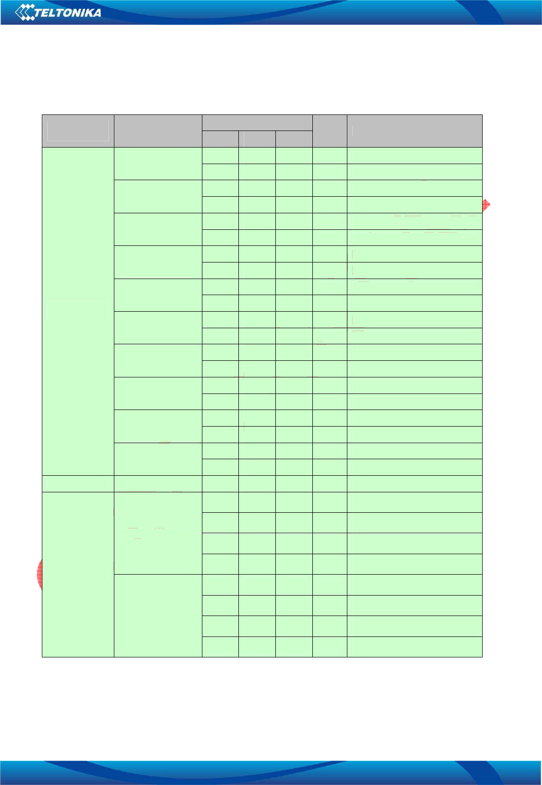
48
TM11Q User Manual v1.0
For
7 layers AG
Internal Use Only
Reproduction forbidden without
Teltonika
, UAB written authorization
–
All Rights Reserved
7.2.2.2 Output characteristics
Voltage
Domain Parameter Limit values Unit Remarks
Min Typ Max
Generic digital
interfaces
L-level output for
output driver class
B slow
0.00 0.40 V I
OL
= +10.0 mA
0.00 0.80 V I
OL
= +15.0 mA
L-level output for
output driver class
B
0.00 0.20 V I
OL
= +2.5 mA
0.00 0.35 V I
OL
= +5.0 mA
L-level output for
output driver class
C
0.00 0.20 V I
OL
= +2.0 mA
0.00 0.35 V I
OL
= +4.0 mA
L-level output for
output driver class
D
0.00 0.20 V I
OL
= +1.0 mA
0.00 0.35 V I
OL
= +2.0 mA
L-level output for
output driver class
E and F
0.00 0.20 V I
OL
= +1.0 mA
0.00 0.35 V I
OL
= +1.5 mA
H-level output for
output driver class
B slow
2.65 2.85 V I
OH
= -10.0 mA
2.50 2.85 V I
OH
= -15.0 mA
H-level output for
output driver class
B
2.65 2.85 V I
OH
= -2.5 mA
2.50 2.85 V I
OH
= -5.0 mA
H-level output for
output driver class
C
2.65 2.85 V I
OH
= -2.0 mA
2.50 2.85 V I
OH
= -4.0 mA
H-level output for
output driver class
D
2.65 2.85 V I
OH
= -1.0 mA
2.50 2.85 V I
OH
= -2.0 mA
H-level output for
output driver class
E and F
2.65 2.85 V I
OH
= -1.0 mA
2.50 2.85 V I
OH
= -1.5 mA
I2C interface L-level output 0.00 0.40 V I
OL
= +3.0 mA
SIM interface
L-level output
0.00 0.20 V VSIM = 1.80 V
I
OL
= +1.0 mA
0.00 0.35 V VSIM = 1.80 V
I
OL
= +1.5 mA
0.00 0.20 V VSIM = 2.85 V
I
OL
= +1.0 mA
0.00 0.35 V VSIM = 2.85 V
I
OL
= +1.5 mA
H-level output
1.60 1.80 V VSIM = 1.80 V
I
OH
= -1.0 mA
1.45 1.80 V VSIM = 1.80 V
I
OH
= -1.5 mA
2.65 2.85 V VSIM = 2.85 V
I
OH
= -1.0 mA
2.50 2.85 V VSIM = 2.85 V
I
OH
= -1.5 mA
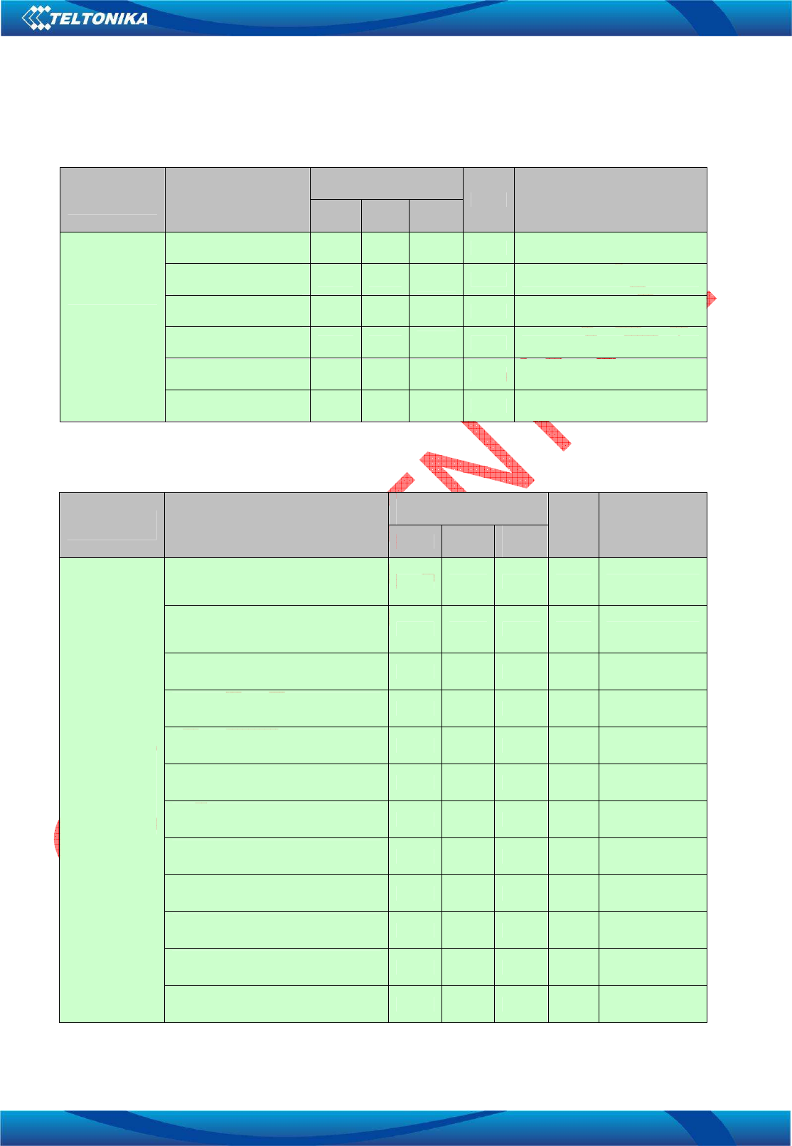
49
TM11Q User Manual v1.0
For
7 layers AG
Internal Use Only
Reproduction forbidden without
Teltonika
, UAB written authorization
–
All Rights Reserved
7.2.2.3 Pad pull-up and pull-down characteristics
Voltage
Domain Parameter Limit values Unit Remarks
Min Typ Max
Generic digital
interfaces or
SIM interface
Pull-up input current for
pull class A -450 uA
Pull-up input current for
pull class B -100 uA
Pull-up input current for
pull class C -30 uA
Pull-down input current
for pull class A 450 uA
Pull-down input current
for pull class B 100 uA
Pull-down input current
for pull class C 30 uA
7.2.2.4 Pad resistance characteristics
Voltage
Domain Parameter Limit values Unit Remarks
Min Typ Max
Generic digital
interfaces
or
I2C interface
or
SIM interface
Pad resistance at 2.5-5.0 mA load
Rising edge for output driver class B
slow
50 Ohm
Pad resistance at 2.5-5.0 mA load
Falling edge for output driver class B
slow
50 Ohm
Pad resistance at 2.5-5.0 mA load
Rising edge for output driver class B 70 Ohm
Pad resistance at 2.5-5.0 mA load
Falling edge for output driver class B 70 Ohm
Pad resistance at 2.0-4.0 mA load
Rising edge for output driver class C 70 Ohm
Pad resistance at 2.0-4.0 mA load
Falling edge for output driver class C 70 Ohm
Pad resistance at 1.0-2.0 mA load
Rising edge for output driver class D 115 Ohm
Pad resistance at 1.0-2.0 mA load
Falling edge for output driver class D 115 Ohm
Pad resistance at 1.0-1.5 mA load
Rising edge for output driver class E 130 Ohm
Pad resistance at 1.0-1.5 mA load
Falling edge for output driver class E 120 Ohm
Pad resistance at 1.0-1.5 mA load
Rising edge for output driver class F 180 Ohm
Pad resistance at 1.0-1.5 mA load
Falling edge for output driver class F 180 Ohm
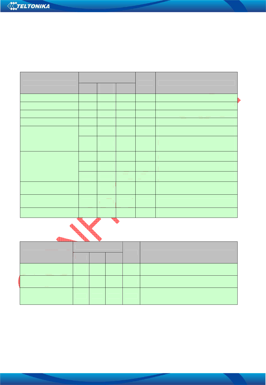
50
TM11Q User Manual v1.0
For
7 layers AG
Internal Use Only
Reproduction forbidden without
Teltonika
, UAB written authorization
–
All Rights Reserved
7.2.3 Audio pins
7.2.3.1 BaseBand audio transmit path characteristics
Parameter Limit values Unit Remarks
Min Typ Max
Differential input voltage 1.03 Vpp
Differential input impedence 50 kOhm
Input capacitance 5 10 pF
Signal to distortion 65 dB
Signal-to-noise ratio
75 dB Gain stage = +12dB
Bandwidth = 300-3900Hz (GSM mode)
72 dB Gain stage = +12dB
Bandwidth = 300-7000Hz (WAMR
mode)
Power supply rejection
66 85 dB Gain stage = +24dB
U
VDD
(t) = 2.5V+0.15V•sin(2π•1kHz•t)
62 dB Gain stage = +18dB
U
VDD
(t) = 2.5V+0.15V•sin(2π•1kHz•t)
45 dB Gain stage = +0dB
U
VDD
(t) = 2.5V+0.15V•sin(2π•1kHz•t)
Cross talk (between Rx and
Tx channel) -65 dB U
TX
(t) = 1.075V+
U
RX
(t) = 0.775V•sin(2π•1kHz•t)
Cut-off frequency of anti-
alias filter 16 kHz
Absolute gain drift ±2 % Variation due to change in supply,
temperature and life time.
7.2.3.2 BaseBand microphone supply characteristics
Parameter Limit values Unit Remarks
Min Typ Max
Output voltage of pin
VMIC 2.20 V Settable to: 1.8 V, 2.0 V, 2.2 V typ.
Microphone supply
current 2.0 mA
Power supply rejection
of microphone supply 75 dB Gain stage = +0dB in crosstalk free conditions
at board level
U
VDD
(t) = 2.6V+0.10V•sin(2π•1kHz•t)
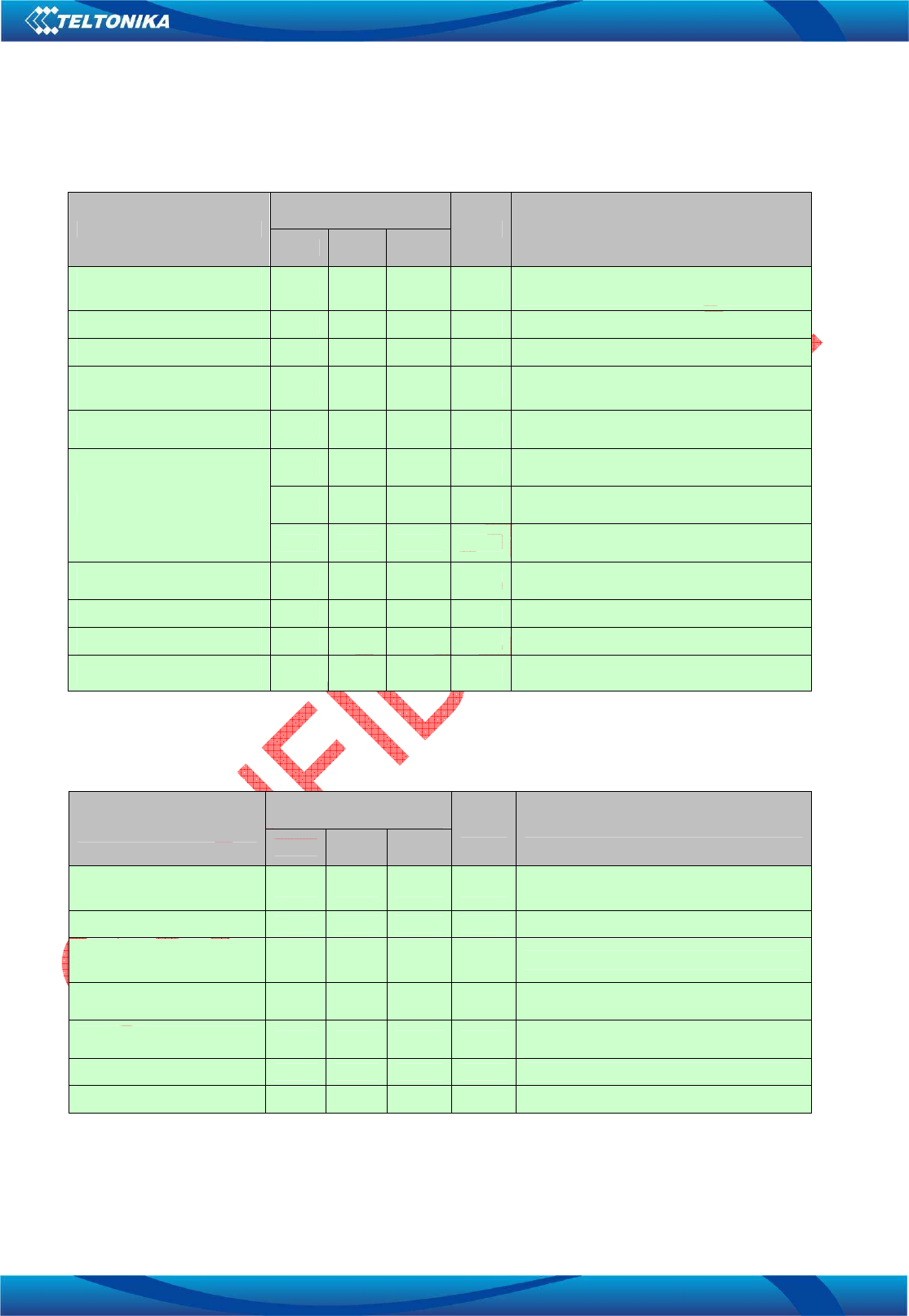
51
TM11Q User Manual v1.0
For
7 layers AG
Internal Use Only
Reproduction forbidden without
Teltonika
, UAB written authorization
–
All Rights Reserved
7.2.3.3 BaseBand low power single-ended audio receive path characteristics
Parameter Limit values Unit Remarks
Min Typ Max
Maximum single-ended
output voltage 1.65 1.85 2.05 Vpp Full scale single-ended open circuit
voltage.
Internal output resistance 1.7 4 Ohm
Output load resistance 16 Ohm
Single-ended output load
capacitance 10 nF
Signal to noise 70 80 dB Load = 16Ω, Gain stage = +0dB,
Input signal = 0dBFS, Code 0, A-weighted
Signal to distortion
60 70 dB Load = 16Ω, Gain stage = +0dB,
Input signal = 0dBFS
60 70 dB Load = 16Ω, Gain stage = +0dB,
Input signal = -1dBFS
60 dB Load = 16Ω, Gain stage = +0dB,
Input signal = -6dBFS
Power supply rejection 60 66 dB Gain stage = +0dB,
U
VDD
(t) = 2.5V+0.15V•sin(2π•1kHz•t)
Passband ripple 0.5 dB f < 0.45 f
s
Stopband attenuation 50 dB f > 0.55 f
s
Absolute gain drift ±2 % Variation due to change in supply,
temperature and life time.
7.2.3.4 BaseBand high power differential audio receive path characteristics
Parameter Limit values Unit Remarks
Min Typ Max
Maximum differential
output voltage 10.4 Vpp Overdrive
Gain stage = +9dB
Output load resistance 8 Ohm
Single-ended output load
capacitance 10 nF
Inductive load 400 uH Between output pins and GND
with series resistance
Signal to noise 70 80 dB Load = 16Ω, Gain stage = +0dB,
Input signal = 0dBFS, Code 0, A-weighted
Signal to distortion 50 dB Load = 8Ω, 350mW
Power supply rejection 60 dB 1kHz
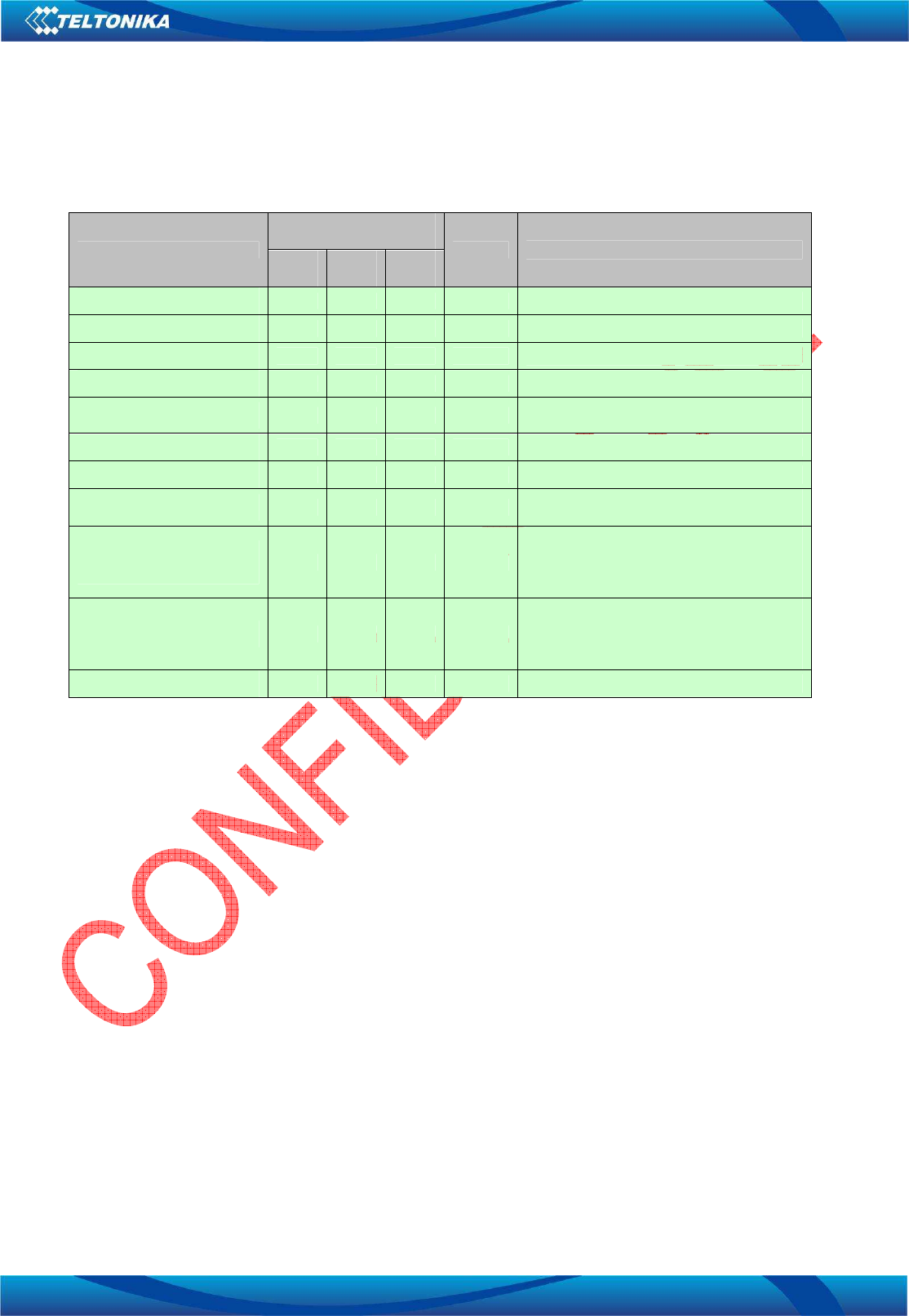
52
TM11Q User Manual v1.0
For
7 layers AG
Internal Use Only
Reproduction forbidden without
Teltonika
, UAB written authorization
–
All Rights Reserved
7.2.4 ADC pins
7.2.4.1 Input characteristics
Parameter Limit values Unit Remarks
Min Typ Max
Resolution 12 Bits
Differential linearity error ±0.5 LSB
Integral linearity error ±4 LSB
Offset error ±10 LSB ADC input = 0V
Absolute gain drift ±2 % Variation due to change in supply,
temperature and life time.
Input voltage span 0 1.92 V
Throughput rate 4 Hz With current ADC SW driver
Input resistance 1 MΩ With respect to AGND.
If mode OFF is selected.
Input resistance in
measurement mode 288 480 672 kOhm
With respect to AGND.
Variation due to process tolerances and
change in supply, temperature, and life
time.
Internal voltage 0.46 0.48 0.50 V
With respect to AGND.
Variation due to process tolerances and
change in supply, temperature, and life
time.
Input leakage current 0.1 uA

53
TM11Q User Manual v1.0
For
7 layers AG
Internal Use Only
Reproduction forbidden without
Teltonika
, UAB written authorization
–
All Rights Reserved
8 Safety Recommendations
Be sure the use of this product is allowed in the country and in the environment required. The use of this
product may be dangerous and has to be avoided in the following areas:
- Where it can interfere with other electronic devices in environments such as hospitals, airports,
aircrafts, etc;
- Where there is risk of explosion such as gasoline stations, oil refineries, etc.
It is responsibility of the user to enforce the country regulation and the specific environment regulation.
Do not disassemble the product; any mark of tampering will compromise the warranty validity.
We recommend following the instructions of the hardware user guides for a correct wiring of the product.
The product has to be supplied with a stabilized voltage limited power source in according EN 60950-1 and
the wiring has to be conforming to the security and fire prevention regulations.
The product is intended for building-in. The requirements for fire enclosure must be evaluated in the end
product. The clearance and creepage distances required by the end product must be withheld when the
product is installed. The cooling of the end product shall not negatively be influenced by the installation of
the product.
The product has to be handled with care, avoiding any contact with the pins because electrostatic
discharges may damage the product itself. Same cautions have to be taken for the SIM, checking carefully
the instruction for its use. Do not insert or remove the SIM when the product is in power saving mode.
The system integrator is responsible of the functioning of the final product; therefore, care has to be taken
to the external components of the module, as well as of any project or installation issue, because the risk of
disturbing the GSM network or external devices or having impact on the security. Should there be any
doubt, please refer to the technical documentation and the regulations in force.
Every module has to be equipped with a proper antenna with specific characteristics. The antenna has to
be installed with care in order to avoid any interference with other electronic devices and has to guarantee
a minimum distance from the body (20 cm). In case of this requirement cannot be satisfied, the system
integrator has to assess the final product against the SAR regulation.
The European Community provides some Directives for the electronic equipments introduced on the
market. All the relevant information’s are available on the European Community website:
http://europa.eu.int/comm/enterprise/rtte/dir99-5.htm
The text of the Directive 99/05 regarding telecommunication equipments is available, while the applicable
Directives (Low Voltage and EMC) are available at:
http://europa.eu.int/comm/enterprise/electr_equipment/index_en.htm