UBS Axcera 430B 1000-Watt VHF High-band Television Transmitter User Manual 430B
UBS-Axcera 1000-Watt VHF High-band Television Transmitter 430B
UserManual.wiki
>
UBS Axcera
>
430B User Manual
Compiled User Manual
Navigation menu
Upload a User Manual
Namespaces
Wiki Guide
HTML
PDF
Info
Views
User Manual
Discussion / Help
Navigation
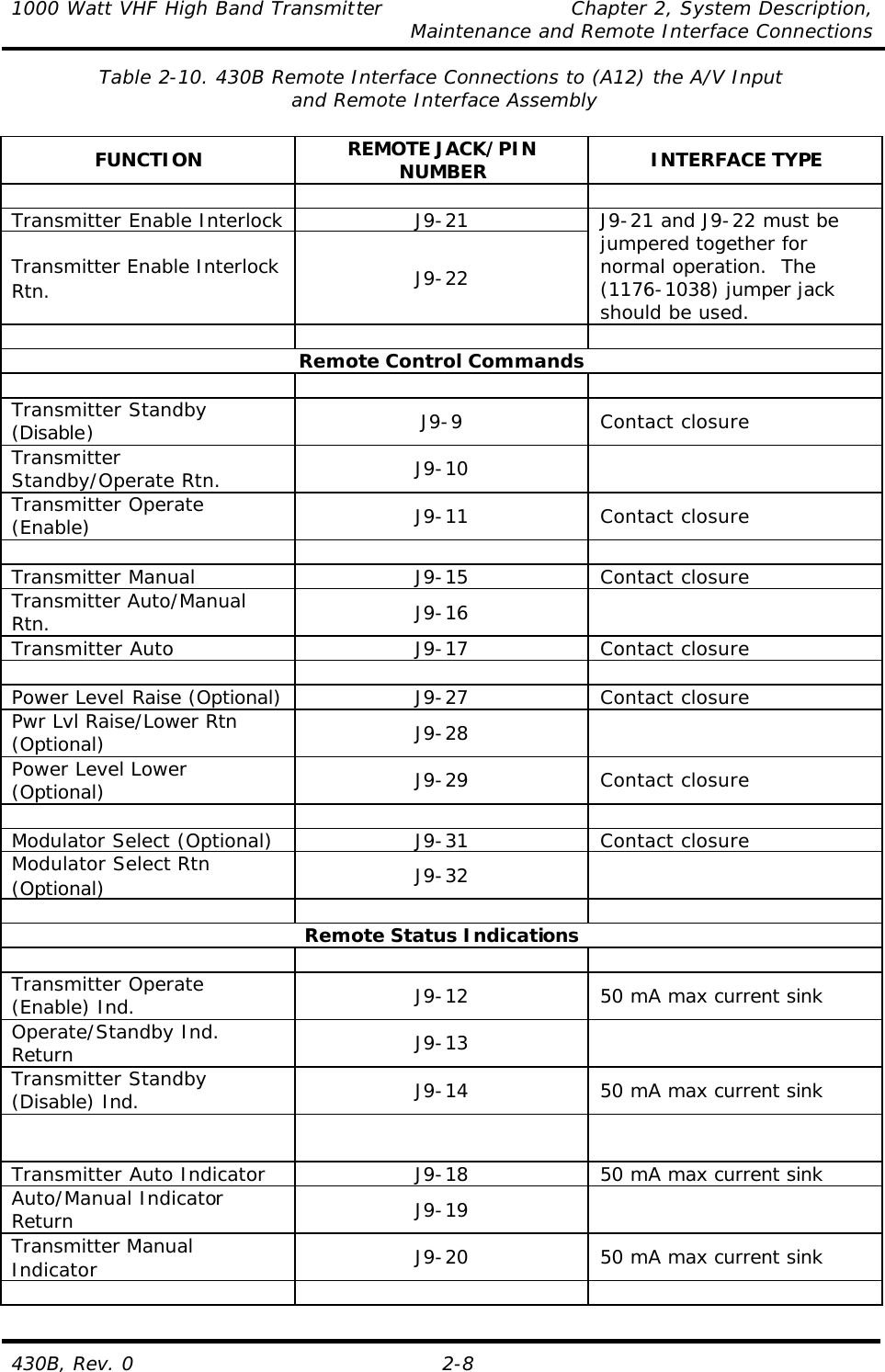
![1000 Watt VHF High Band Transmitter Chapter 5, Detailed Alignment Procedures 430B, Rev. 0 5-3 receiver tray is present in the system). DS5 is always on with no receiver. The ALC is muted when the transmitter is in Standby. To monitor the ALC, turn off the two amplifier on/off circuit breakers on the AC distribution assembly at the rear of the cabinet and switch the transmitter to Operate. Adjust the power adjust gain pot on the front panel of the VHF exciter tray to obtain +0.8 VDC on the front panel meter in the ALC position. On the ALC board (1265-1305), move jumper W3 on J6 to the Manual position, between pins 2 and 3, and adjust R87 on the ALC board for +0.8 VDC on the front panel meter in the ALC position. Move jumper W3 back to Auto (between pins 1 and 2); this is the normal operating position. The detected IF signal level at J19-2 of the ALC board is connected to the transmitter control board that distributes the level to the two VHF amplifier trays where it is used as a reference for the automatic gain control (AGC) in each amplifier tray. 5.1.4 VHF H.B. Exciter Tray Board level Adjustments 5.1.4.1 (Optional) 4.5-MHz Composite Input Kit If the (optional) 4.5-MHz composite input kit is purchased, the tray is capable of operating by using either the 4.5-MHz composite input or the baseband audio and video inputs. The kit adds the (A24) composite 4.5-MHz filter board (1227-1244; Appendix D) and the (A25) 4.5-MHz bandpass filter board (1265-1307; Appendix D) to the transmitter. When the 4.5 MHz intercarrier signal generated by the 4.5 MHz composite input has been selected by the 4.5 MHz composite input kit, the 4.5-MHz generated by the aural IF synthesizer board is not used. When the 4.5 MHz intercarrier signal generated by the baseband video and audio inputs with baseband has been selected by the 4.5 MHz composite input kit, the composite 4.5 MHz filter board and the 4.5 MHz bandpass filter board are not used. The tray has been factory tuned and should not need any alignments to achieve normal operation. To align the tray for the 4.5 MHz composite input, apply the 4.5 MHz composite input, with the test signals used as needed, to the video input jack (J1 or J2 [loop-through connections]) on the rear of the tray. Select the 4.5 MHz composite input by removing the baseband select from J7-6 and J7-7 on the rear of the tray. To align the exciter using baseband video and audio inputs, apply the baseband video, with the test signals used as needed, to the video input jack (J2) and the baseband audio to the proper baseband audio input on the A/V input & remote interface panel. For balanced audio input, connect TB1-1(+), TB1-2(grnd), and TB1-3 (-). For composite/stereo audio, connect the composite audio input jack (J6). Connect a baseband select from J7-6 and J7-7 on the rear of the exciter tray. 5.1.4.1.1 (Optional) (A24) Composite 4.5-MHz Filter Board (1227-1244; Appendix D) This board is part of the 4.5-MHz input kit and will only function properly with a 4.5-MHz composite input signal and the 4.5-MHz composite input selected. To align this board: 1. Connect the test signal from an envelope delay measurement set to the video input of the tray at J1 or J2. 2. Connect an oscilloscope to jack J7, video out, between the J7 center pin and pin 1 or 3 (ground). Adjust C21, frequency response, if needed, for the best frequency response. Adjust R32, video gain, for a signal level of 1 Vpk-pk on the oscilloscope.](https://usermanual.wiki/UBS-Axcera/430B/User-Guide-402870-Page-56.png)
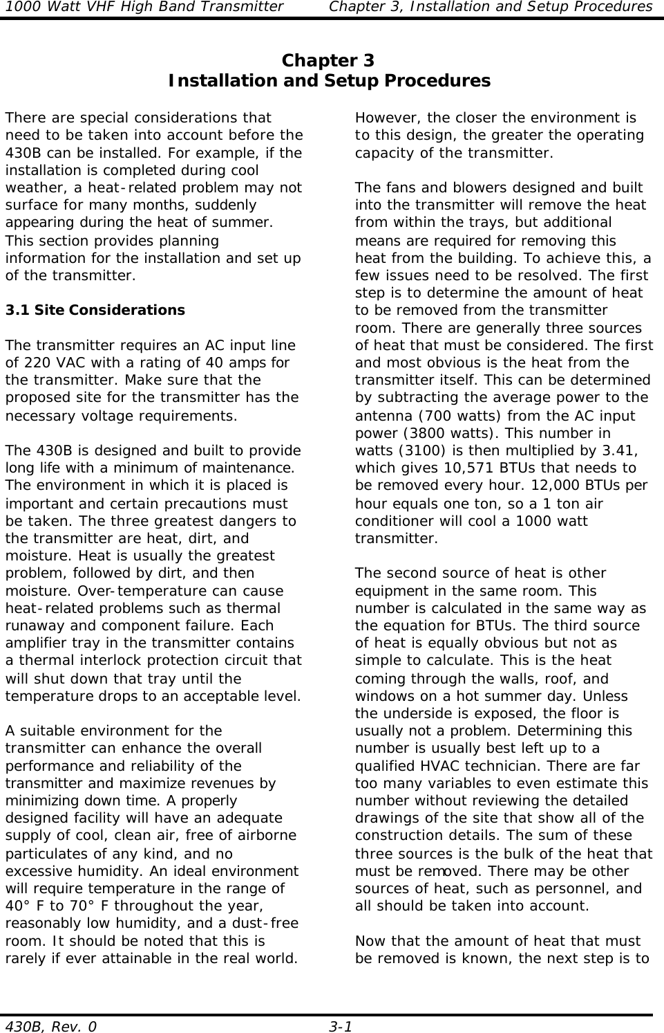
![1000 Watt VHF High Band Transmitter Chapter 5, Detailed Alignment Procedures 430B, Rev. 0 5-11 The idling current, no RF drive applied, of the device Q1 is set for 250 mA. To set the current, remove the RF drive, measure the voltage across R20 (two 1Ω resistors in parallel on the filter/amplifier board) and adjust R13 for .125 volts (using Ohms’ Law: [E=I x R] : [E=250 mA x .5 Ω] : E=125 mV). 5.2.4 (A2-A2) VHF High Band Amplifier Board (P10-VHF-H; Appendix D) This board is supplied by Delta RF Technology, Inc. Refer to the data sheets in the subassembly section of this manual for more information. The board has approximately 19 dB of gain and the output is typically +31 dBm. 5.2.5 (A3-A1) Overdrive Protection Board (1198-1601; Appendix D) The level of the RF input and output of the (A3-A1) overdrive protection board (1198-1601) should be +31 dBm during normal operation. To set up the overdrive circuit, check that the output power level of the transmitter is at 100% and adjust R11 on the board for a reading of .4 VDC at TP1. Increase the output power level of the transmitter to 110%, sync only, and adjust R12 until the output power begins to drop off. Return the output power level of the transmitter to 100%. 5.2.6 (A3-A2) VHF High Band Amplifier Board (P200-VHF-H; Appendix D) This board is supplied by Delta RF Technology, Inc. Refer to the data sheets in the subassembly section of this manual for more information. The board has approximately 14 dB of gain and the output is typically +45 dBm. 5.2.7 (A3-A3) 3 Way Splitter Board (1301161; Appendix D) This board contains no tuning adjustments. The board takes the +45 dBm input and splits it into three equal +40 dBm outputs. 5.2.8 (A4-A1 thru A3) VHF Output Amplifier Pallets (P400-VHF-H; Appendix D) These boards are supplied by Delta RF Technology, Inc. Refer to the data sheets in the subassembly section of this manual for more information. Each board has approximately 13 dB of gain and the output is typically +53.3 dBm. 5.2.9 (A5-A1) 3 Way Combiner Assembly (1301157; Appendix D) There are no adjustments to the (A5-A1) 3 way combiner assembly. The three +53.3 dBm inputs are combined to produce the 600 watts peak of sync + aural output (+57.8 dBm) at the RF output jack J5 of the combiner. J5 of the combiner connects to J2 the RF Output Jack of the VHF Amplifier Tray. 5.2.10 Calibration of the Visual Plus Aural Output Power and VSWR Cutback of the VHF amplifier tray Check that a dummy load of at least 600 watts is connected to the output of the tray that is to be calibrated. Place switch S1 on the AGC control board in the Manual position before beginning the setup. To adjust the visual output power levels: 1. Remove the J16 cable from (A5) the sync tip clamp/modulator board (1265-1302) in the exciter tray. Set Manual AGC switch S1, on the (A13) AGC control board (1142-1601) in the VHF amplifier tray, to the Manual position. 2. Connect a sync and black test signal to the video input jack of the remote](https://usermanual.wiki/UBS-Axcera/430B/User-Guide-402870-Page-64.png)