UBS Axcera CLV2TD-4 Low Band VHF Digital Broadcast Transmitter User Manual
UBS-Axcera Low Band VHF Digital Broadcast Transmitter
UserManual.wiki
>
UBS Axcera
>
CLV2TD 4 User Manual
User Manual
Navigation menu
Upload a User Manual
Namespaces
Wiki Guide
HTML
PDF
Info
Views
User Manual
Discussion / Help
Navigation

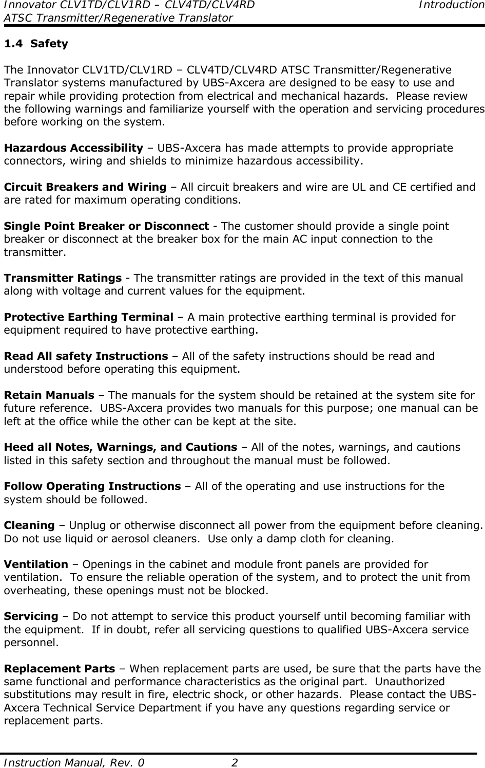
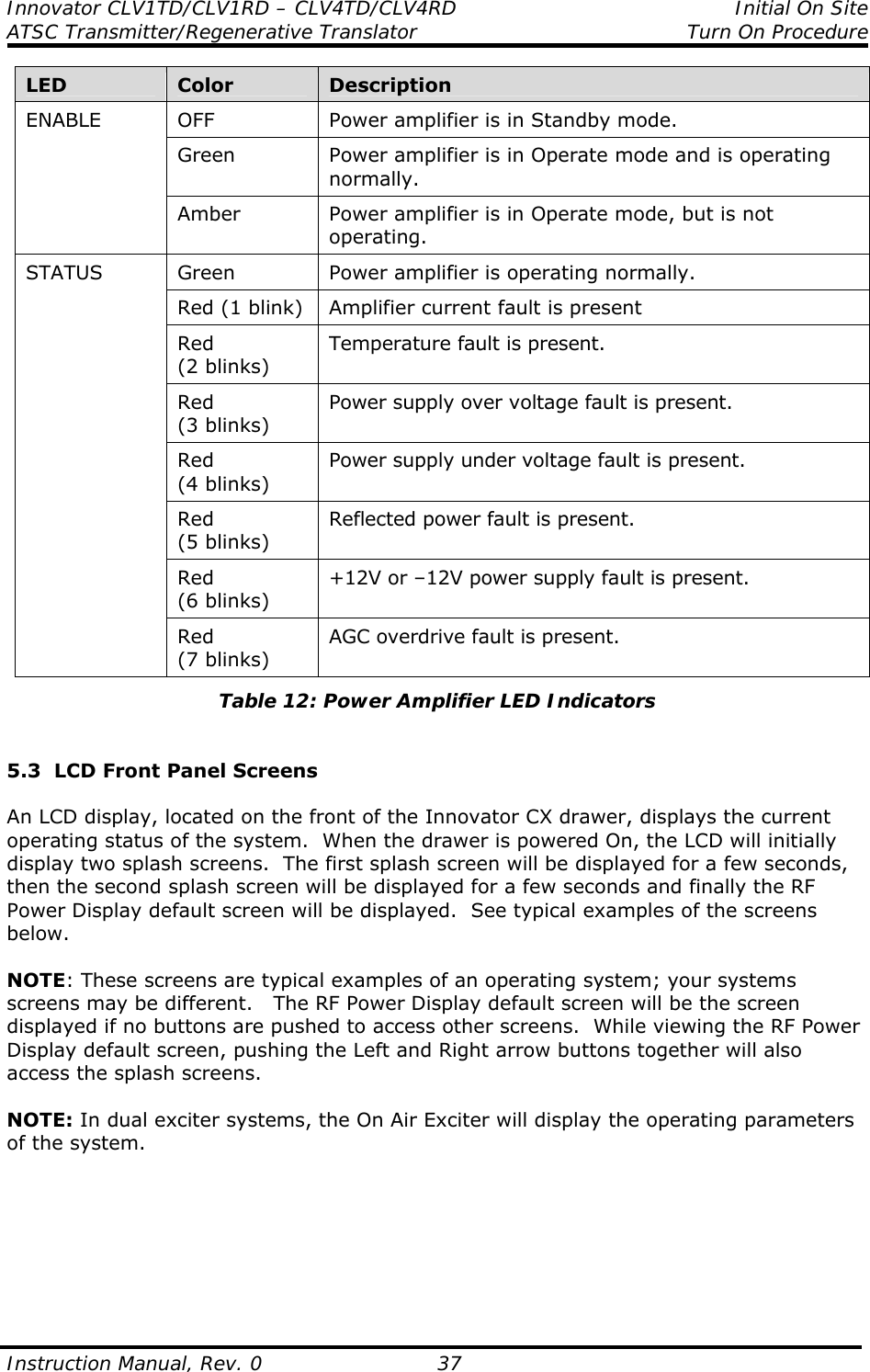
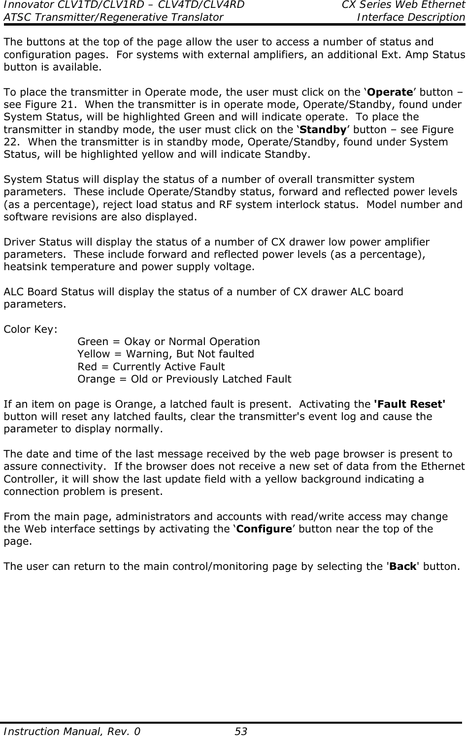
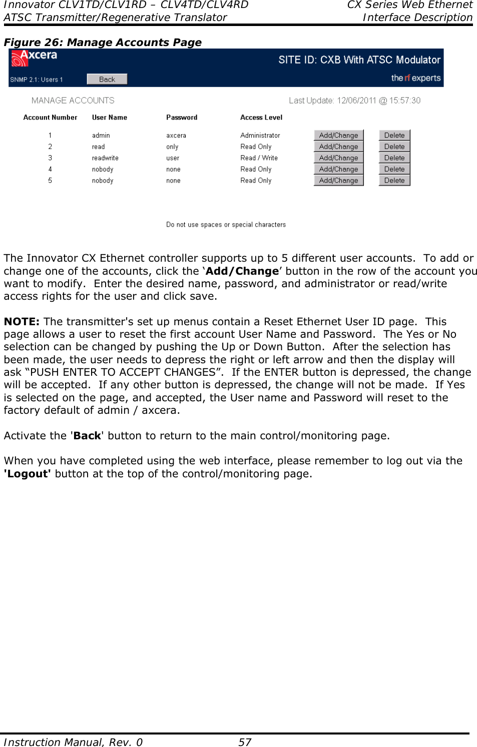
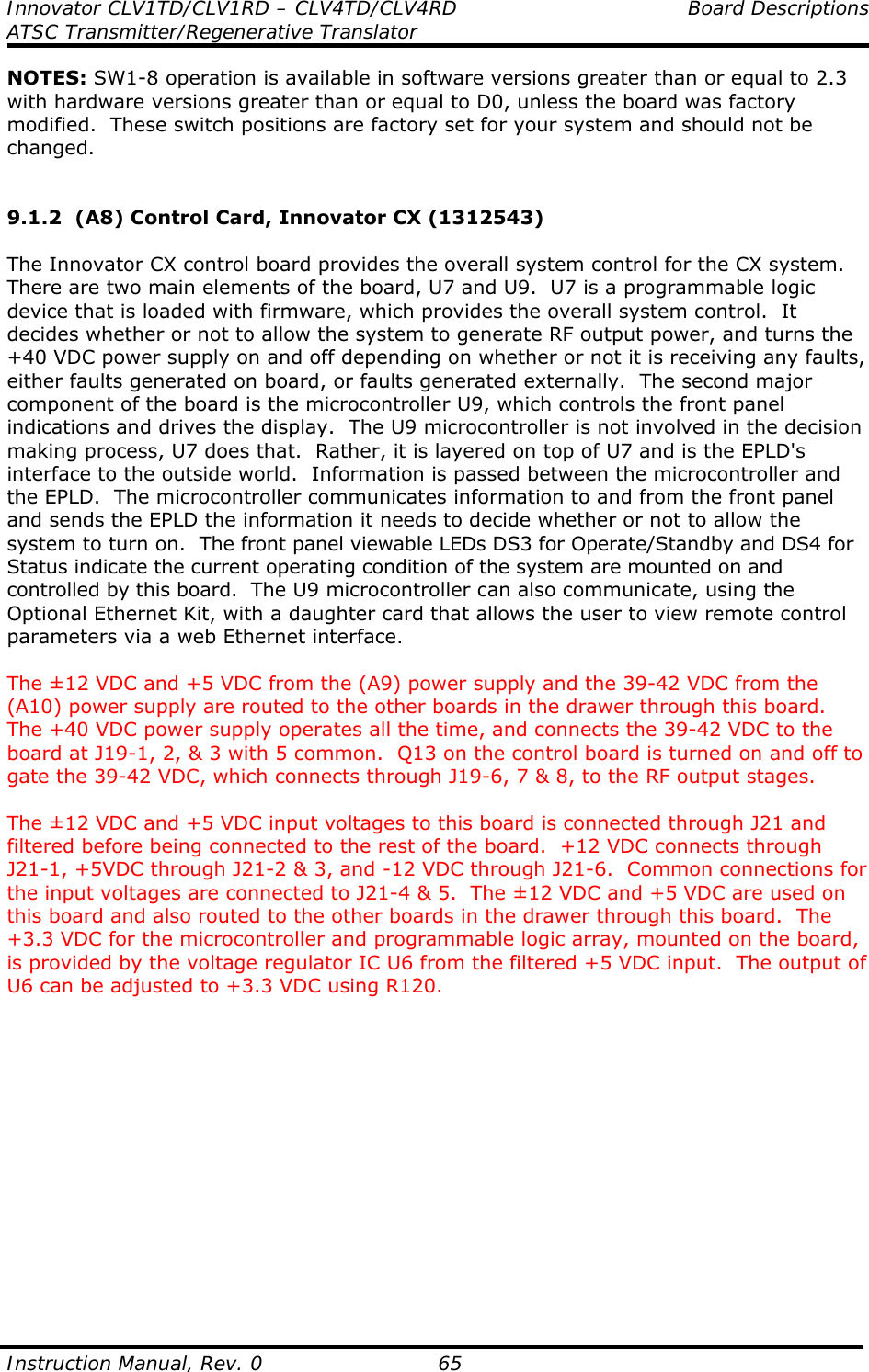
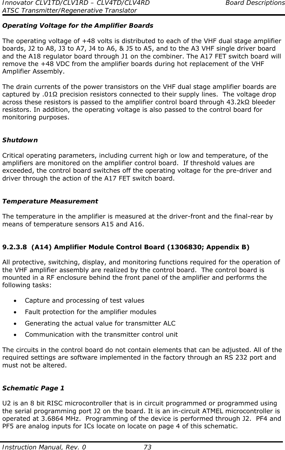
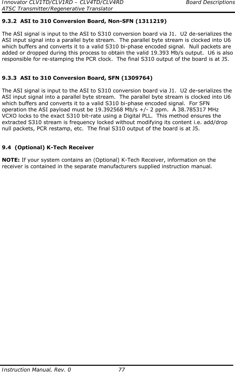
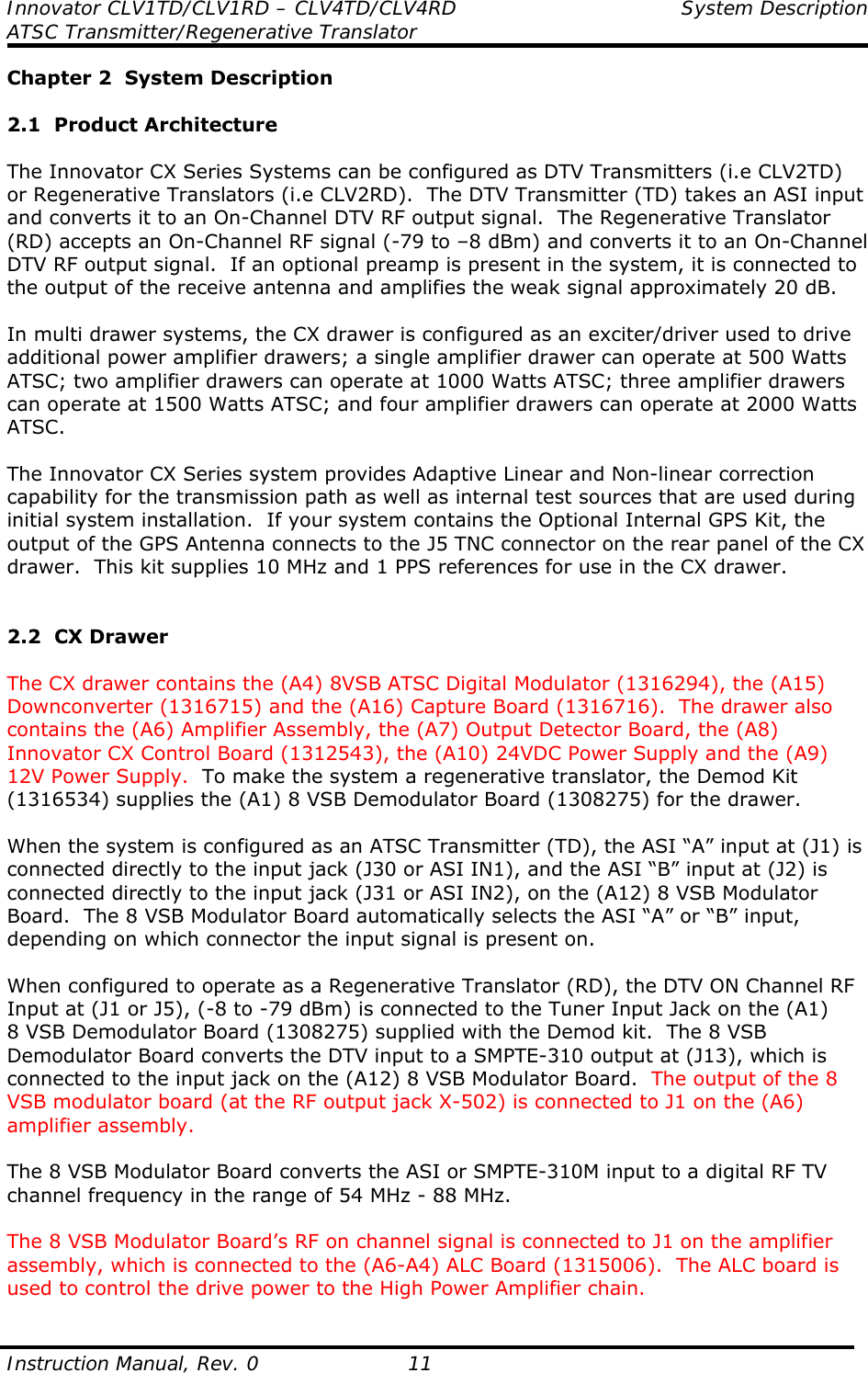
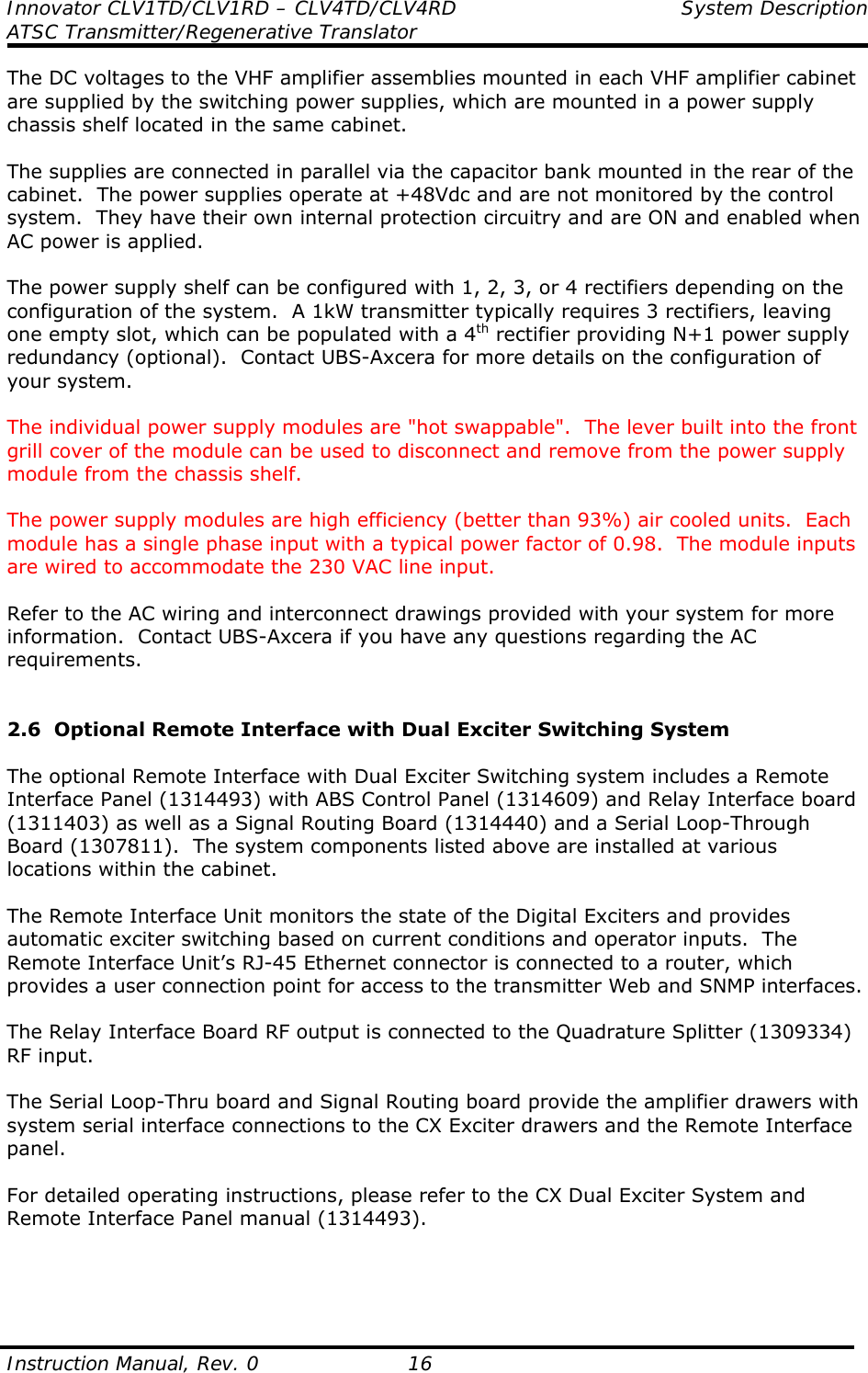
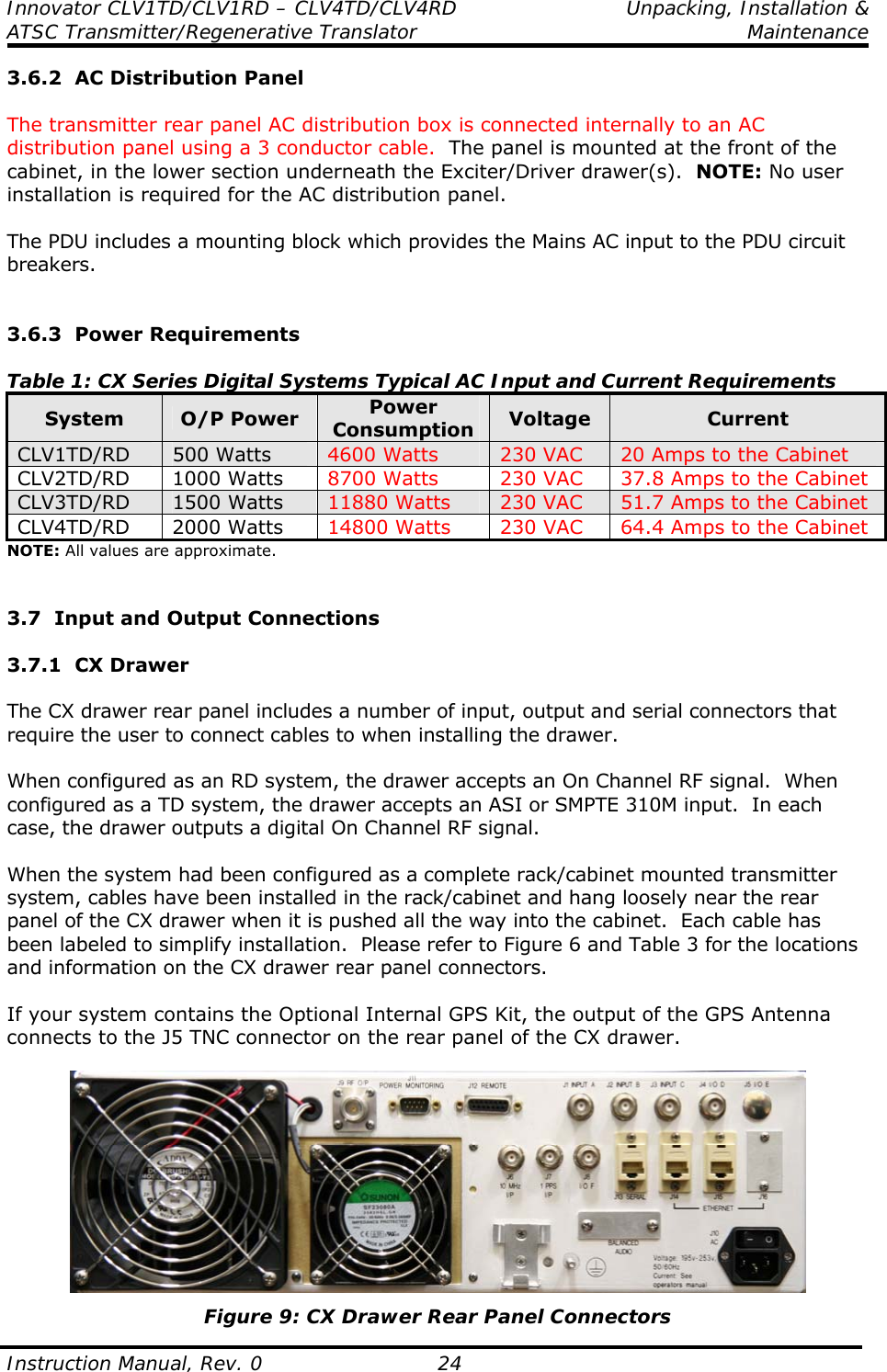
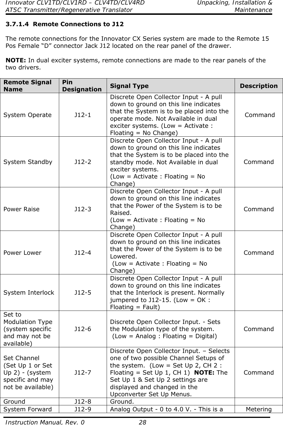
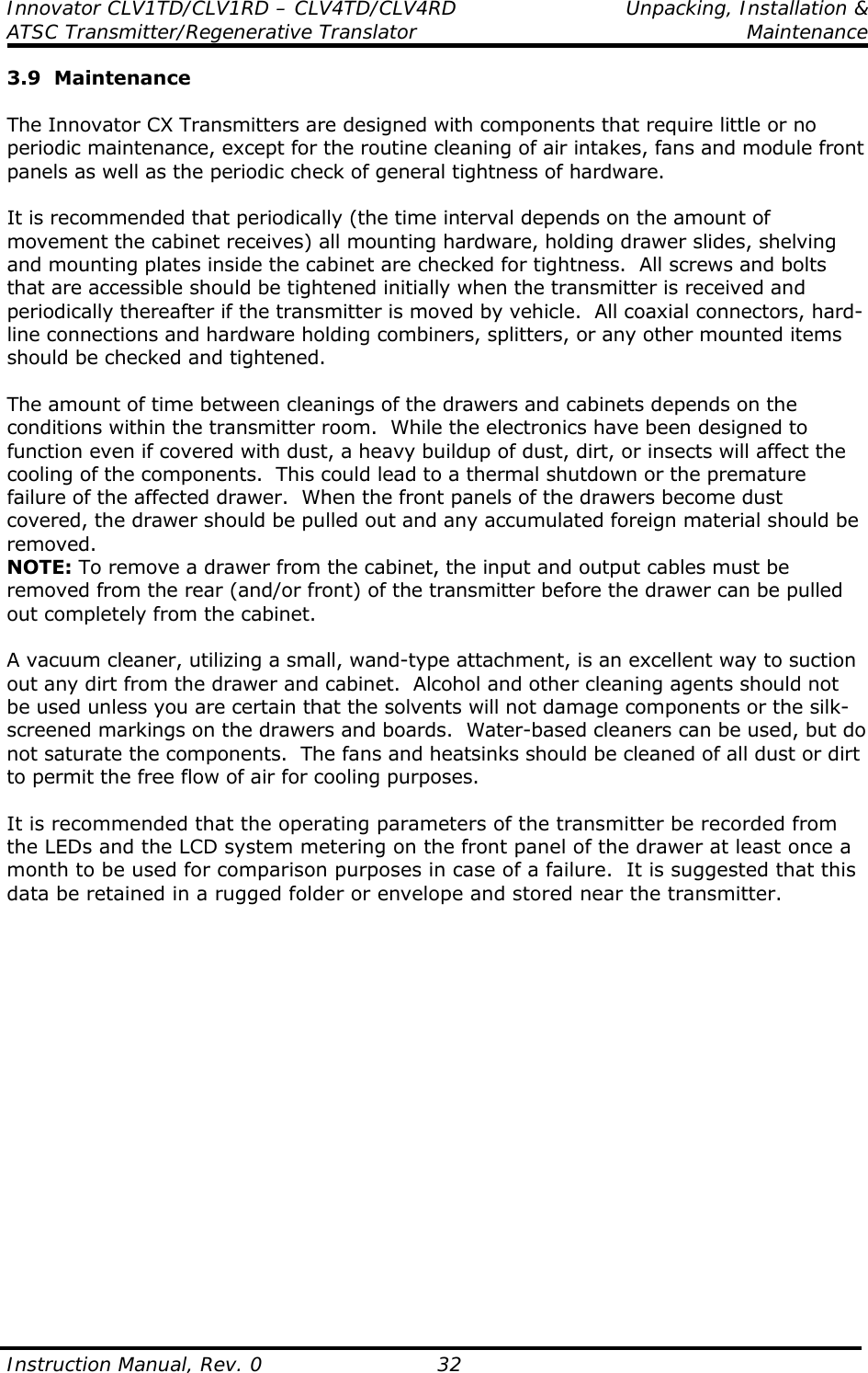
![Innovator CLV1TD/CLV1RD – CLV4TD/CLV4RD Introduction ATSC Transmitter/Regenerative Translator Instruction Manual, Rev. 0 7 dBm, dBw, dBmV, dBµV, & VOLTAGE EXPRESSED IN WATTS 50 Ohm System WATTS PREFIX dBm dBw dBmV dBµV VOLTAGE 1,000,000,000,000 1 TERAWATT +150 +120 100,000,000,000 100 GIGAWATTS +140 +110 10,000,000,000 10 GIGAWATTS +130 +100 1,000,000,000 1 GIGAWATT +120 + 99 100,000,000 100 MEGAWATTS +110 + 80 10,000,000 10 MEGAWATTS +100 + 70 1,000,000 1 MEGAWATT + 90 + 60 100,000 100 KILOWATTS + 80 + 50 10,000 10 KILOWATTS + 70 + 40 1,000 1 KILOWATT + 60 + 30 100 1 HECTROWATT + 50 + 20 50 + 47 + 17 20 + 43 + 13 10 1 DECAWATT + 40 + 10 1 1 WATT + 30 0 + 77 +137 7.07V 0.1 1 DECIWATT + 20 - 10 + 67 +127 2.24V 0.01 1 CENTIWATT + 10 - 20 + 57 +117 0.707V 0.001 1 MILLIWATT 0 - 30 + 47 +107 224mV 0.0001 100 MICROWATTS - 10 - 40 0.00001 10 MICROWATTS - 20 - 50 0.000001 1 MICROWATT - 30 - 60 0.0000001 100 NANOWATTS - 40 - 70 0.00000001 10 NANOWATTS - 50 - 80 0.000000001 1 NANOWATT - 60 - 90 0.0000000001 100 PICOWATTS - 70 -100 0.00000000001 10 PICOWATTS - 80 -110 0.000000000001 1 PICOWATT - 90 -120 TEMPERATURE CONVERSION °F = 32 + [(9/5) °C] °C = [(5/9) (°F - 32)]](https://usermanual.wiki/UBS-Axcera/CLV2TD-4/User-Guide-2052672-Page-12.png)
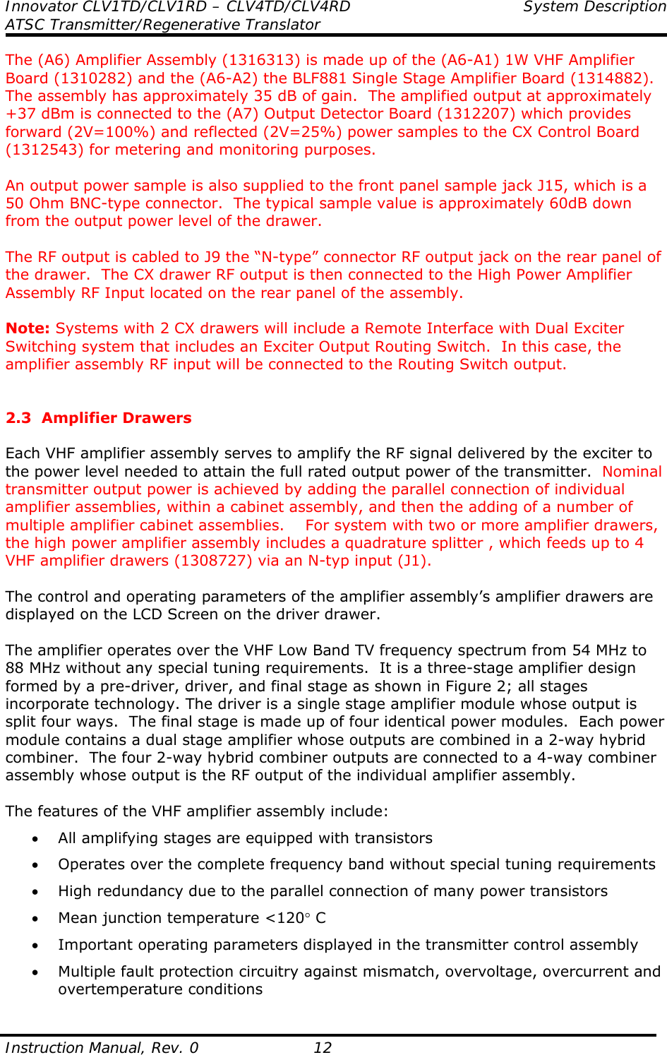
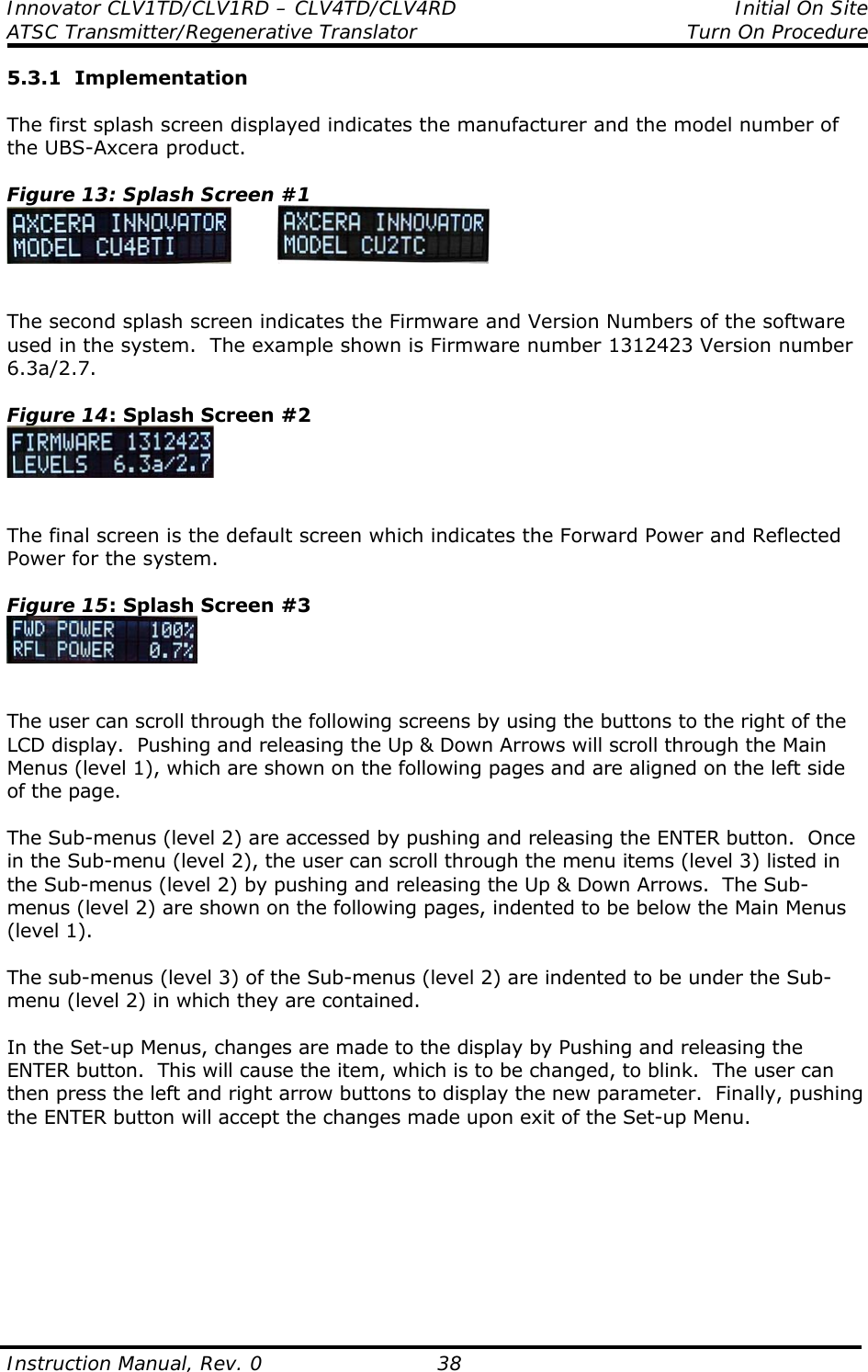
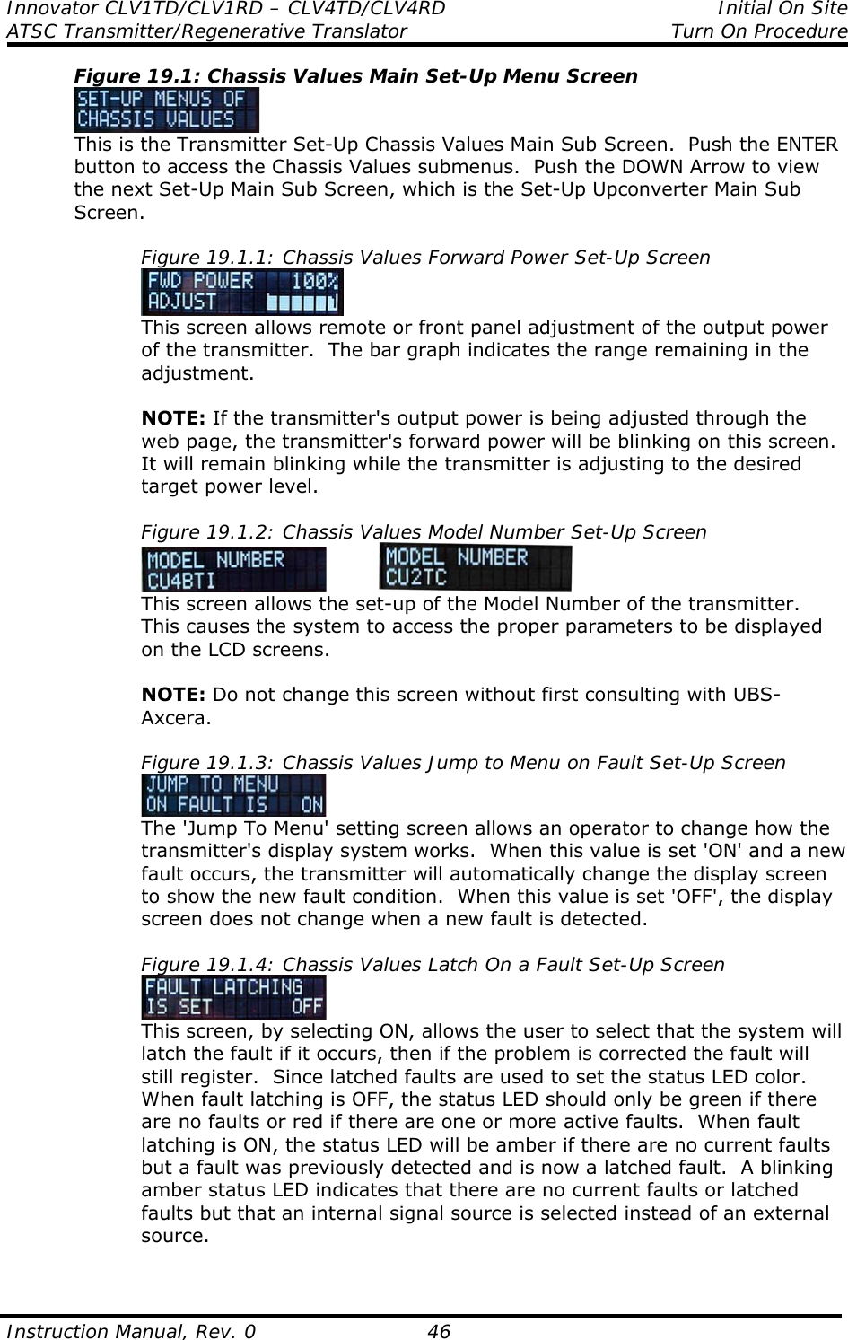
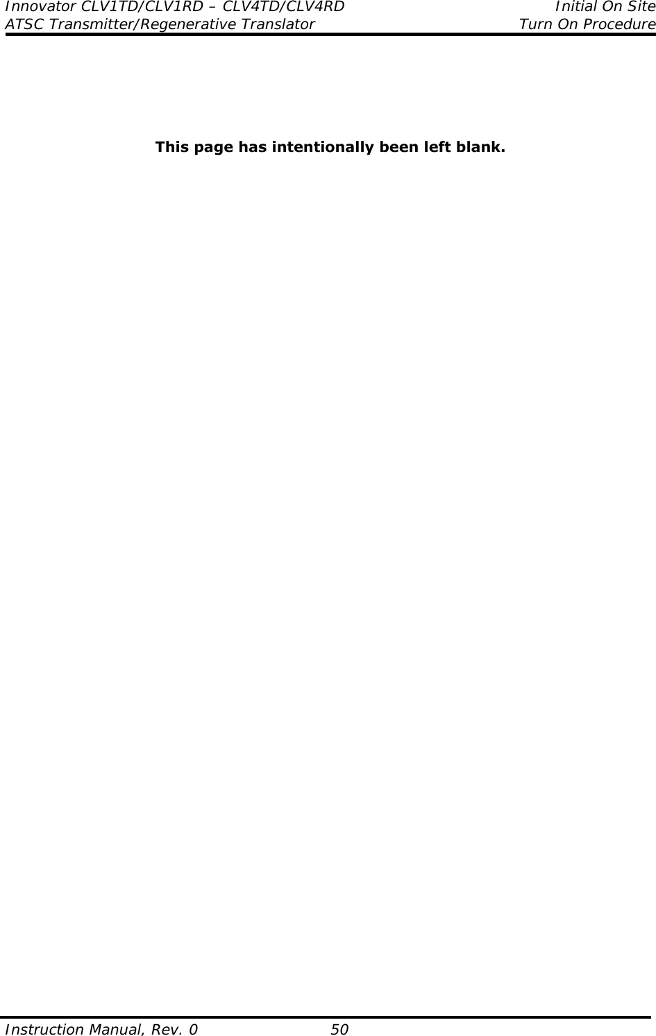
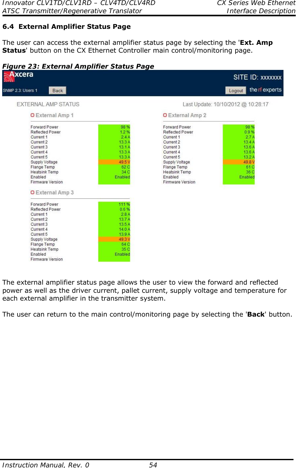
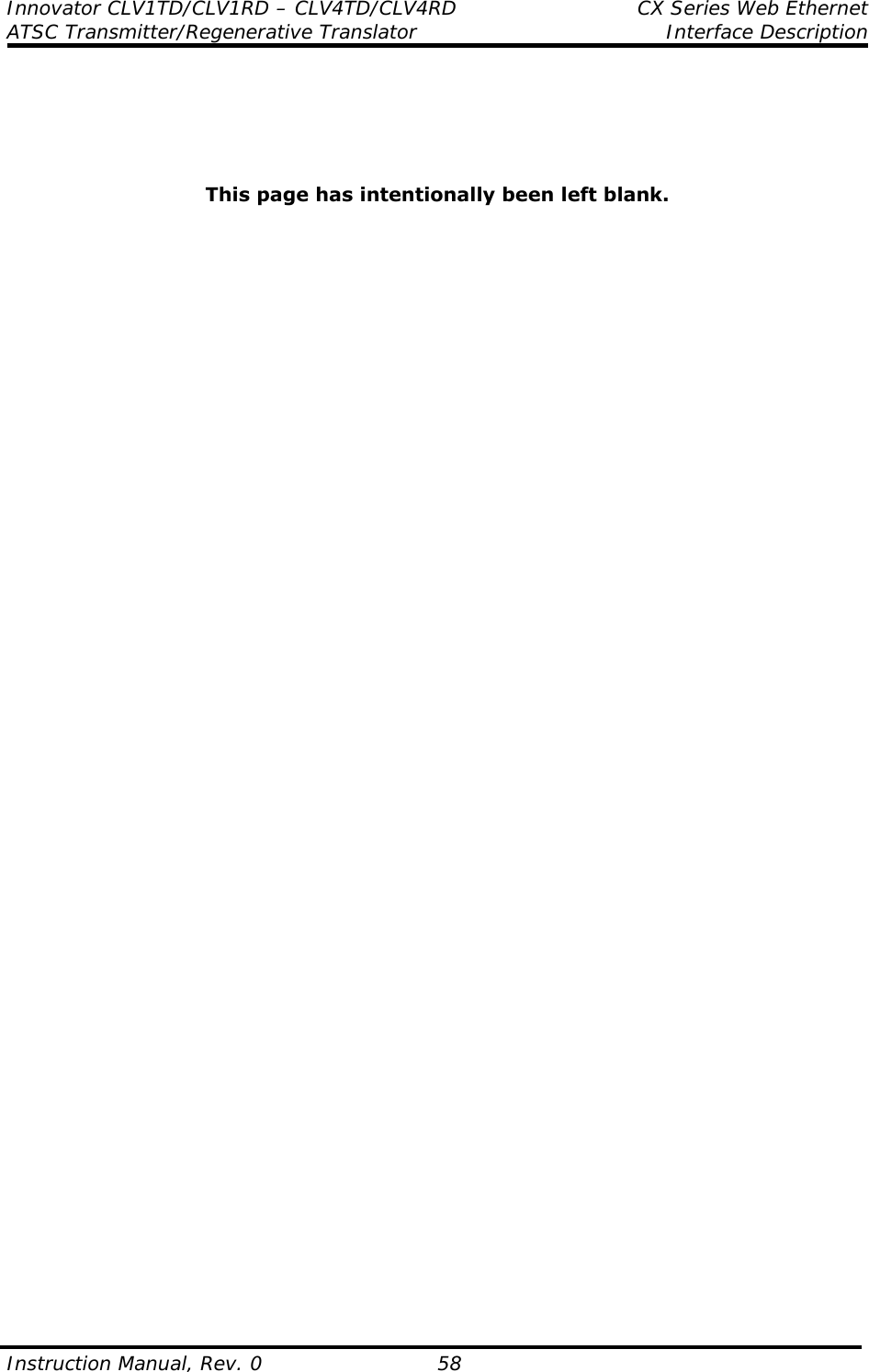
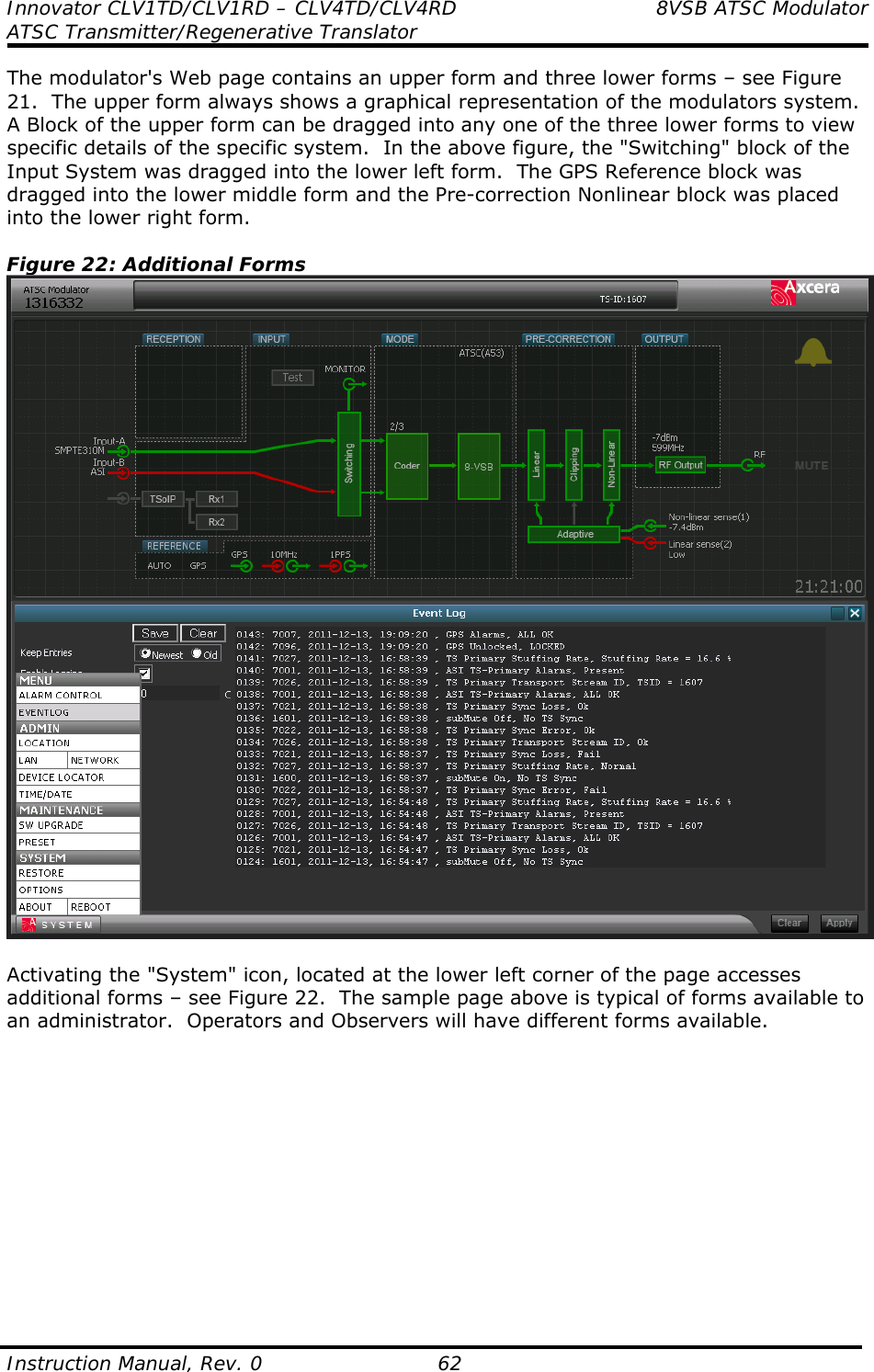
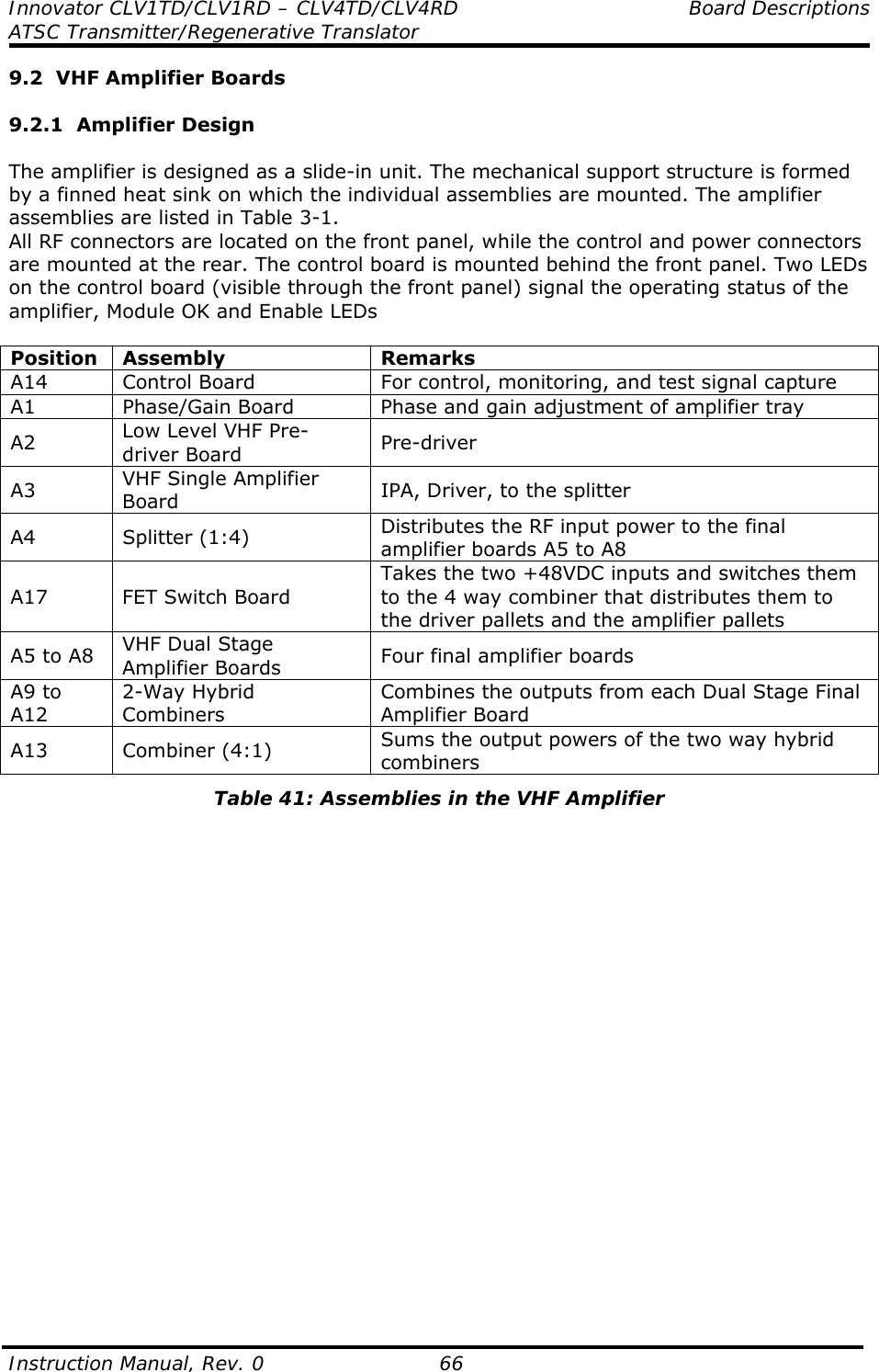
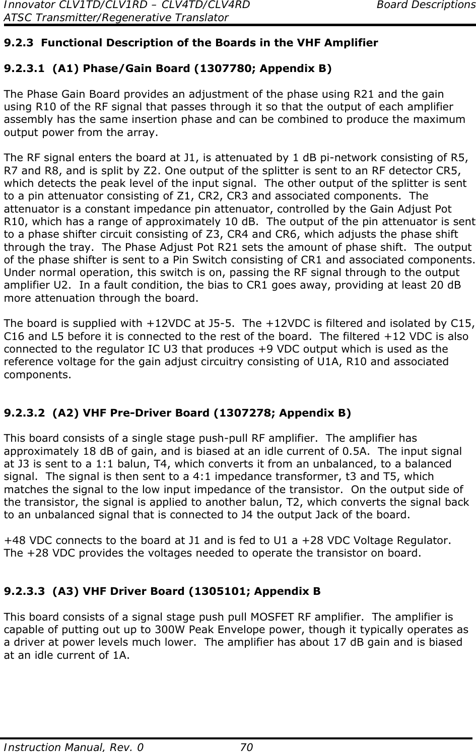
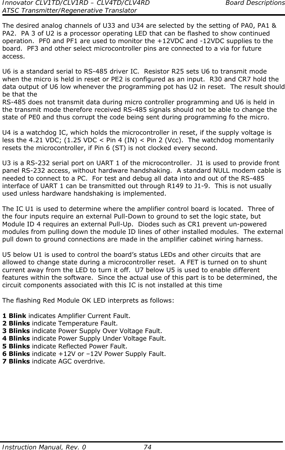
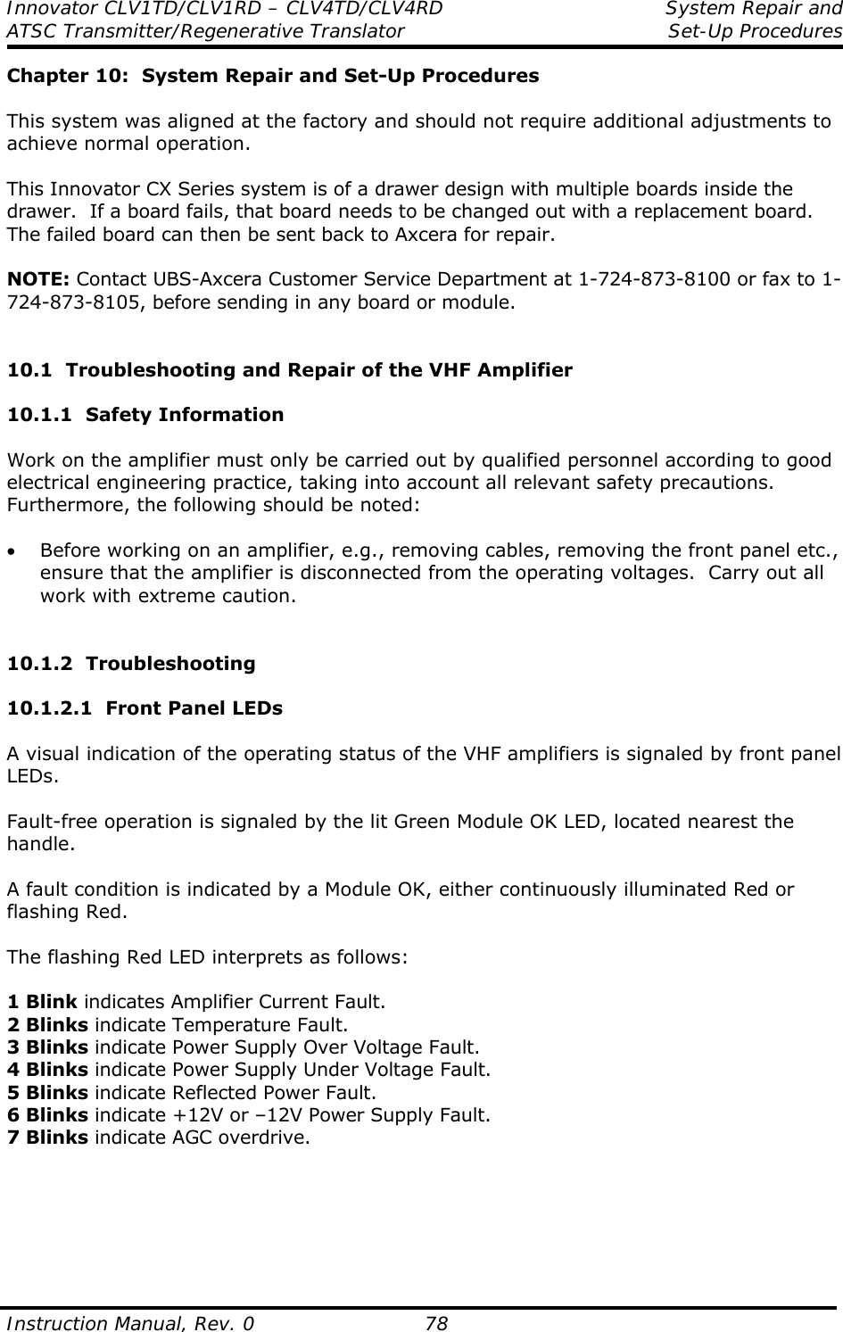
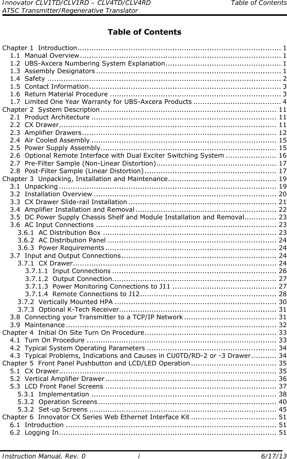
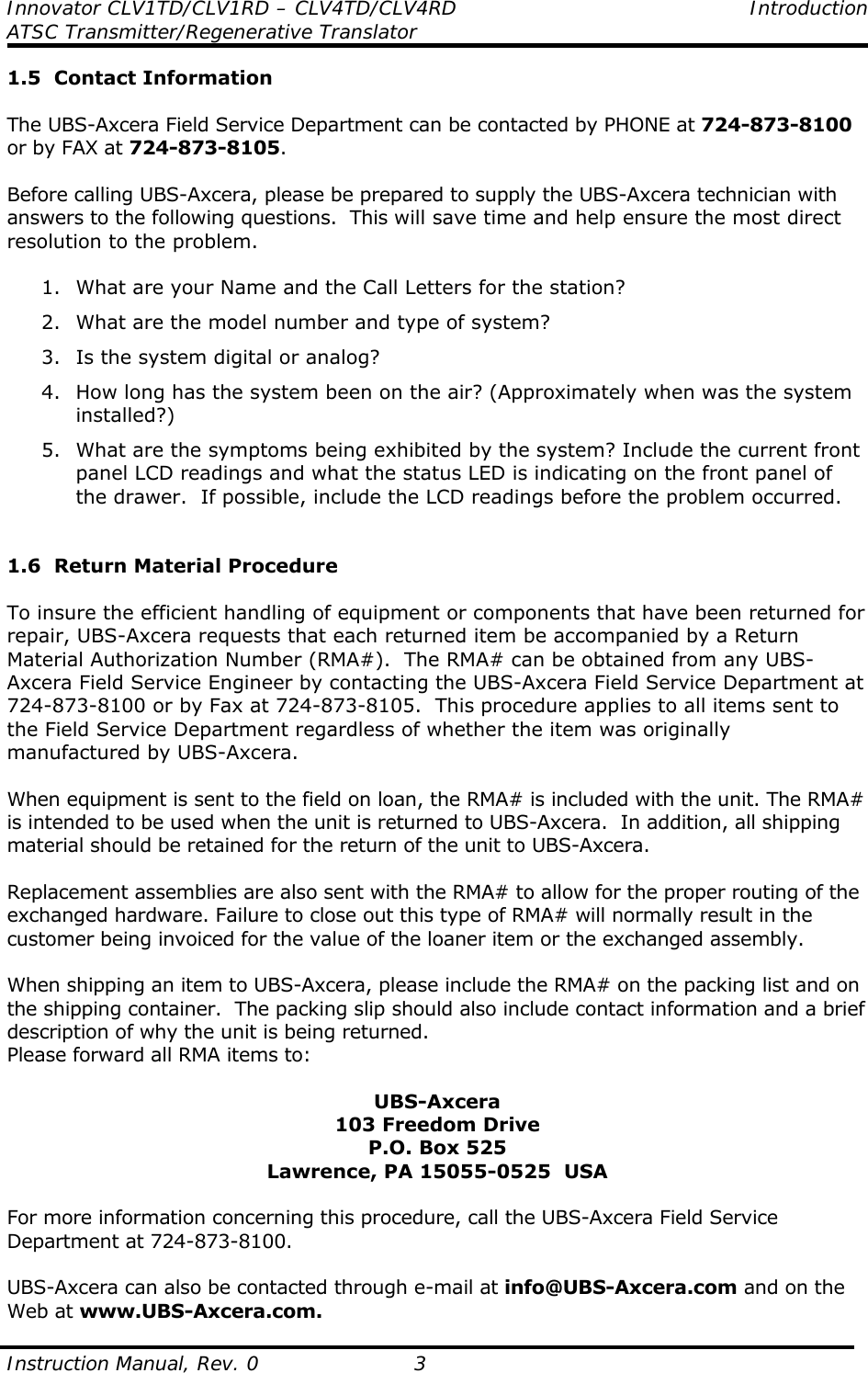
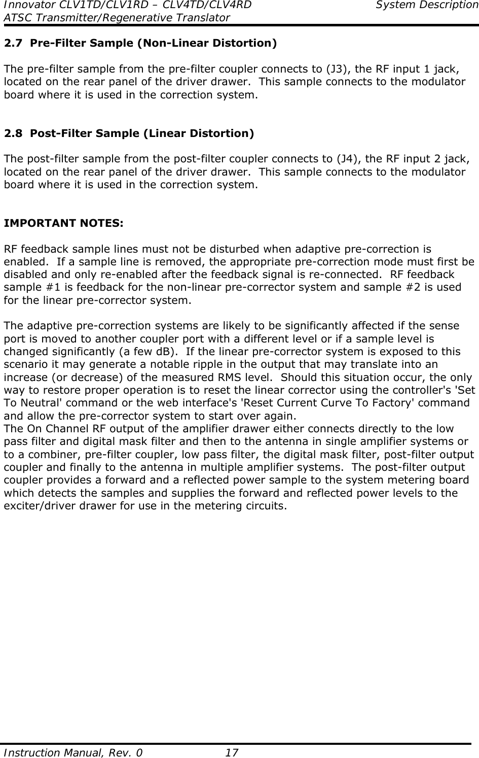
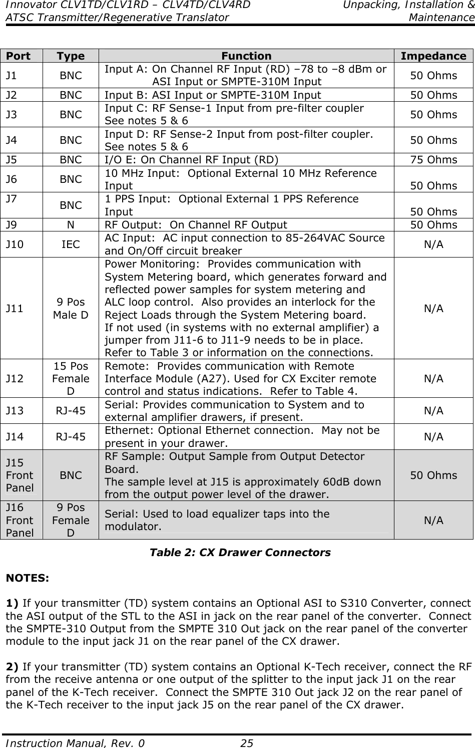
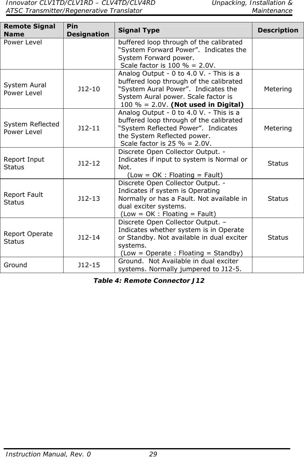
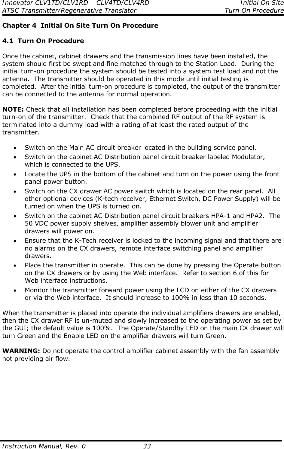
![Innovator CLV1TD/CLV1RD – CLV4TD/CLV4RD System Description ATSC Transmitter/Regenerative Translator Instruction Manual, Rev. 0 13 The amplifier possesses multiple fault-protection circuits that prevent damage to the power transistors during critical operating conditions, such as high mismatch, overtemperature, overcurrent, or overvoltage. Important operating parameters, such as drain currents, operating voltages, RF powers, and temperatures are polled and displayed in the transmitter control assembly. Figure 2: VHF LB Amplifier Assembly The paralleling network of the amplifier is arranged so that it continues to operate at reduced power if a module fails. The remaining available power is given by: Prem = Pnom ⋅ ([m - n] / m)2 where: Prem = remaining power Pnom = nominal power m = number of modules n = number of failed modules Figure 3: Remaining Power after Failure of Amplifier Modules](https://usermanual.wiki/UBS-Axcera/CLV2TD-4/User-Guide-2052672-Page-18.png)
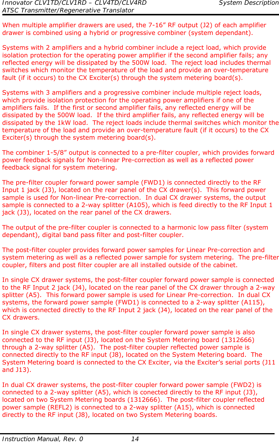
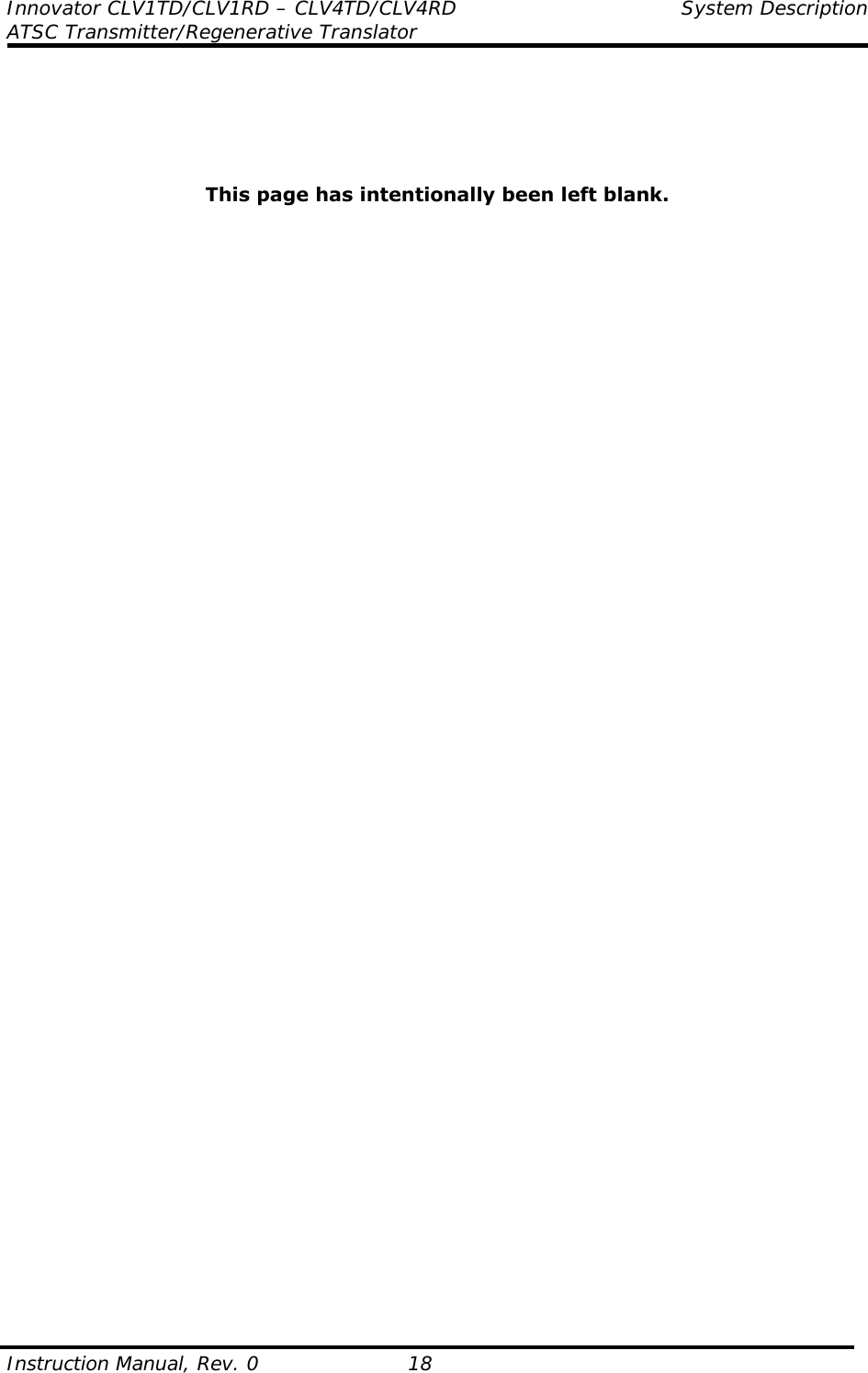
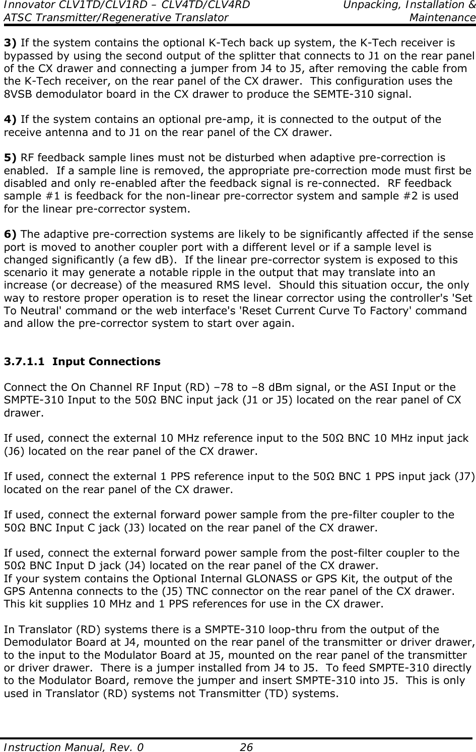
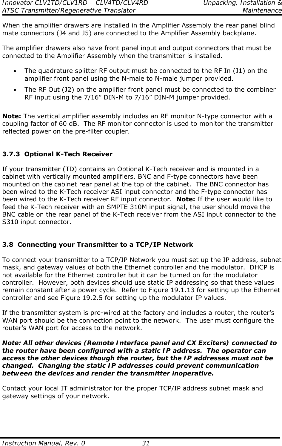
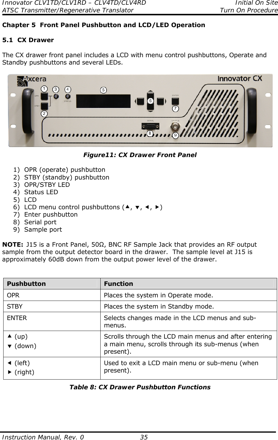
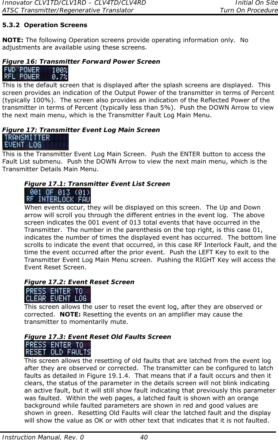
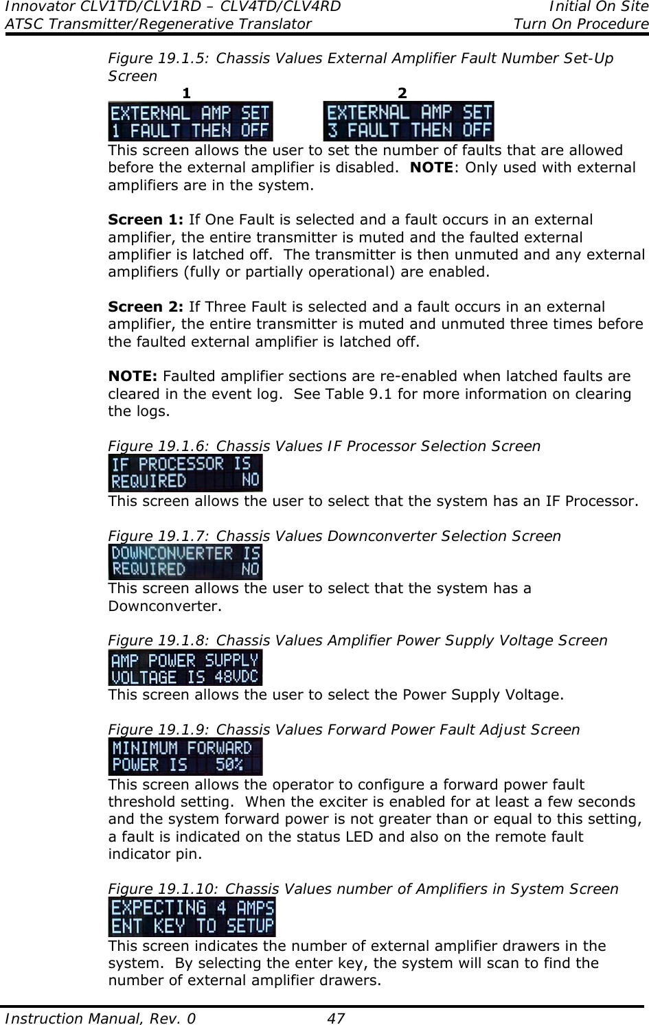
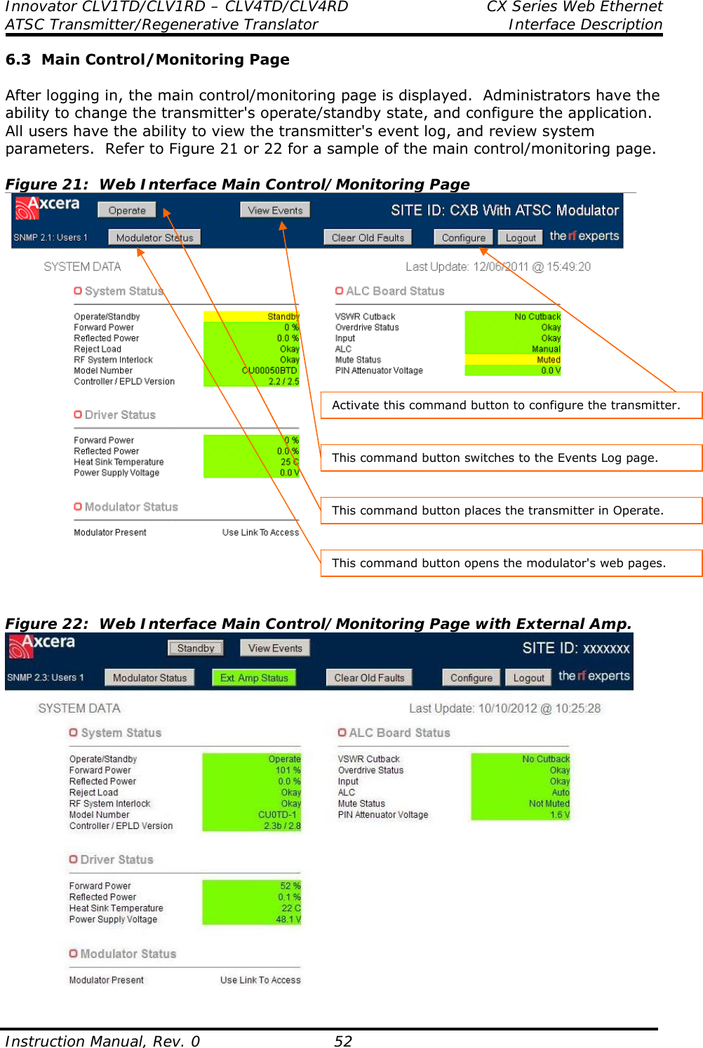
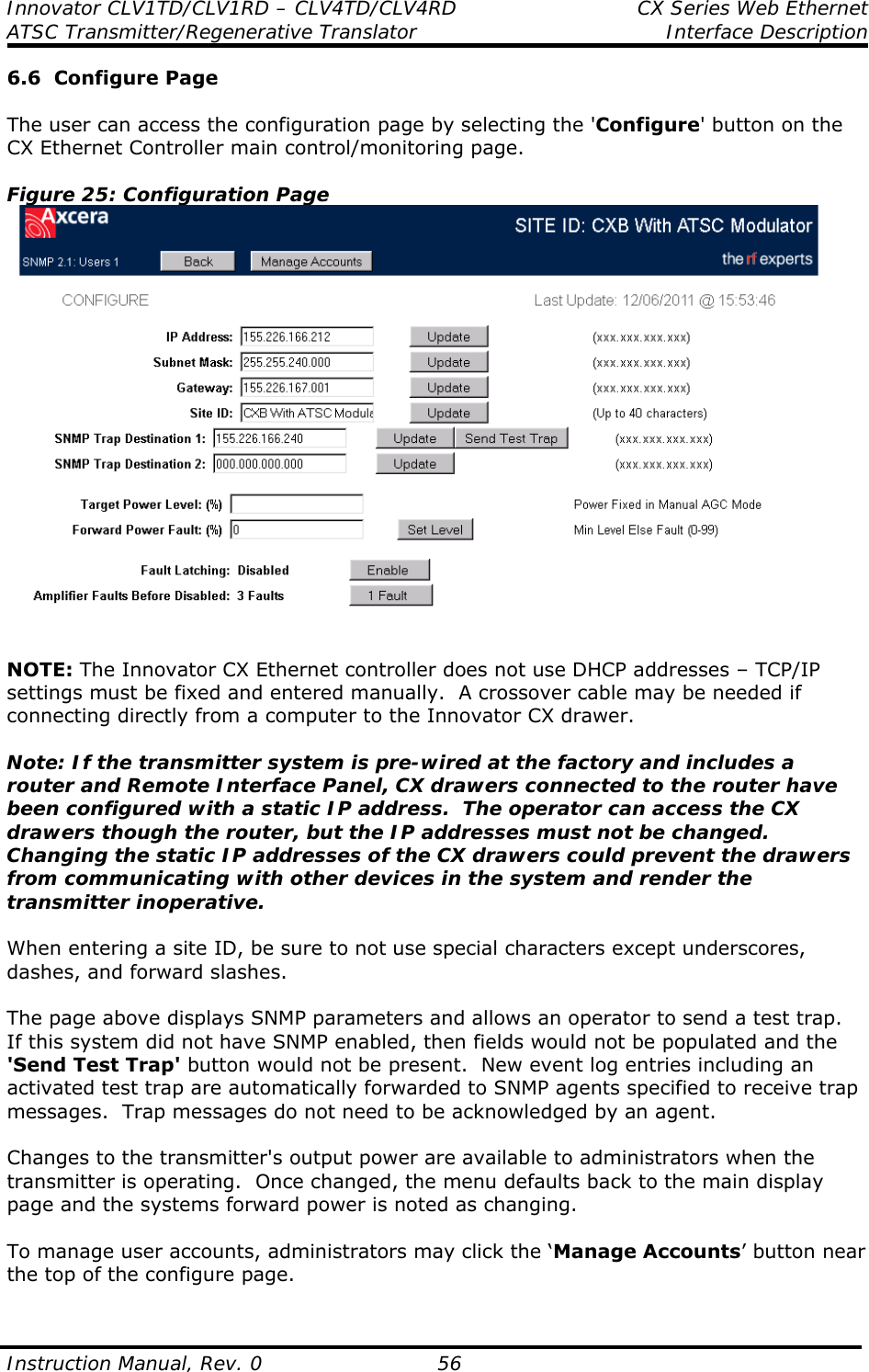
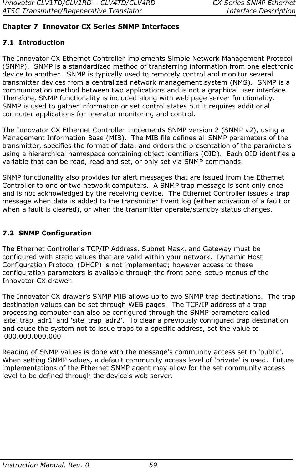
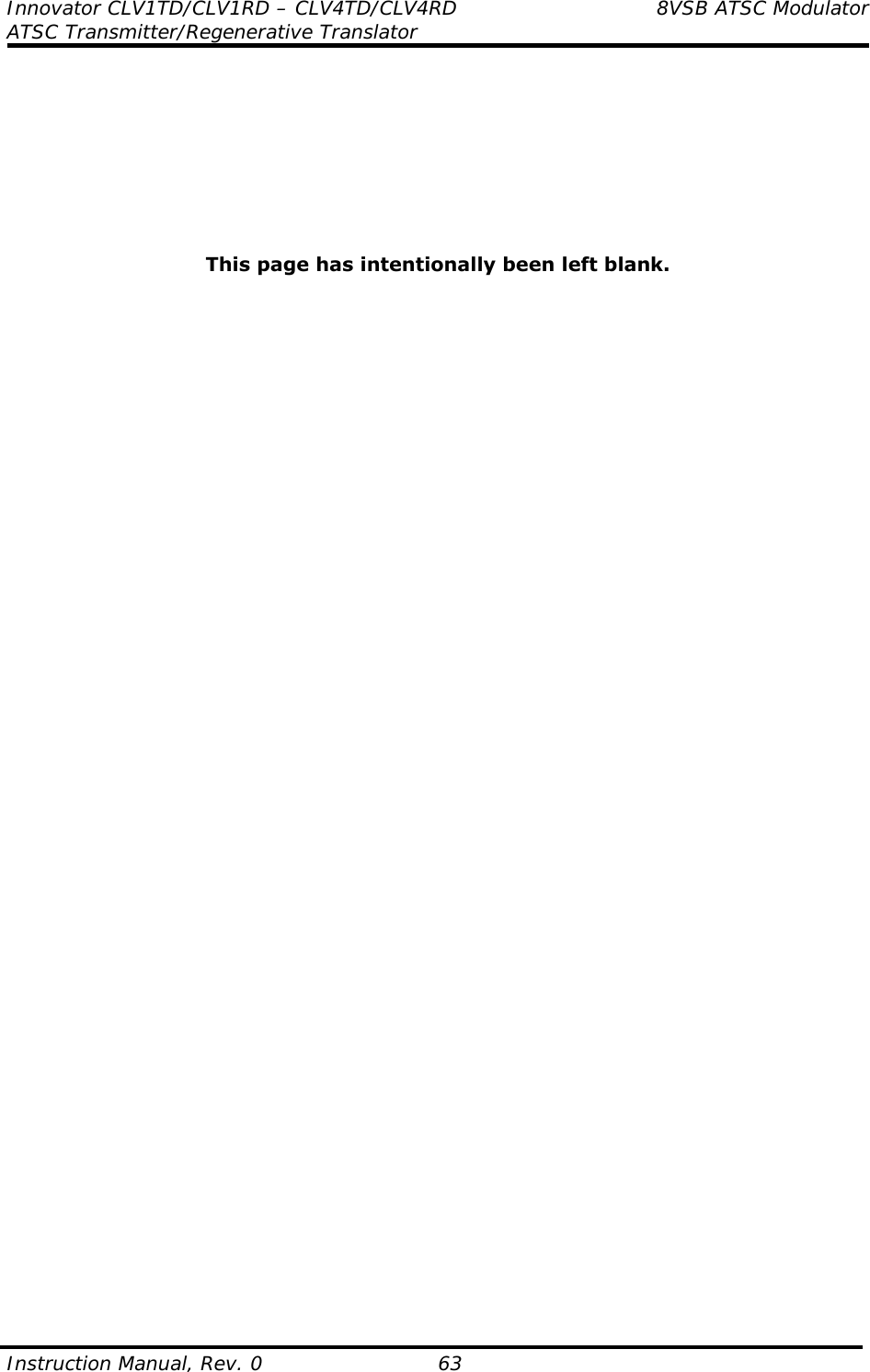
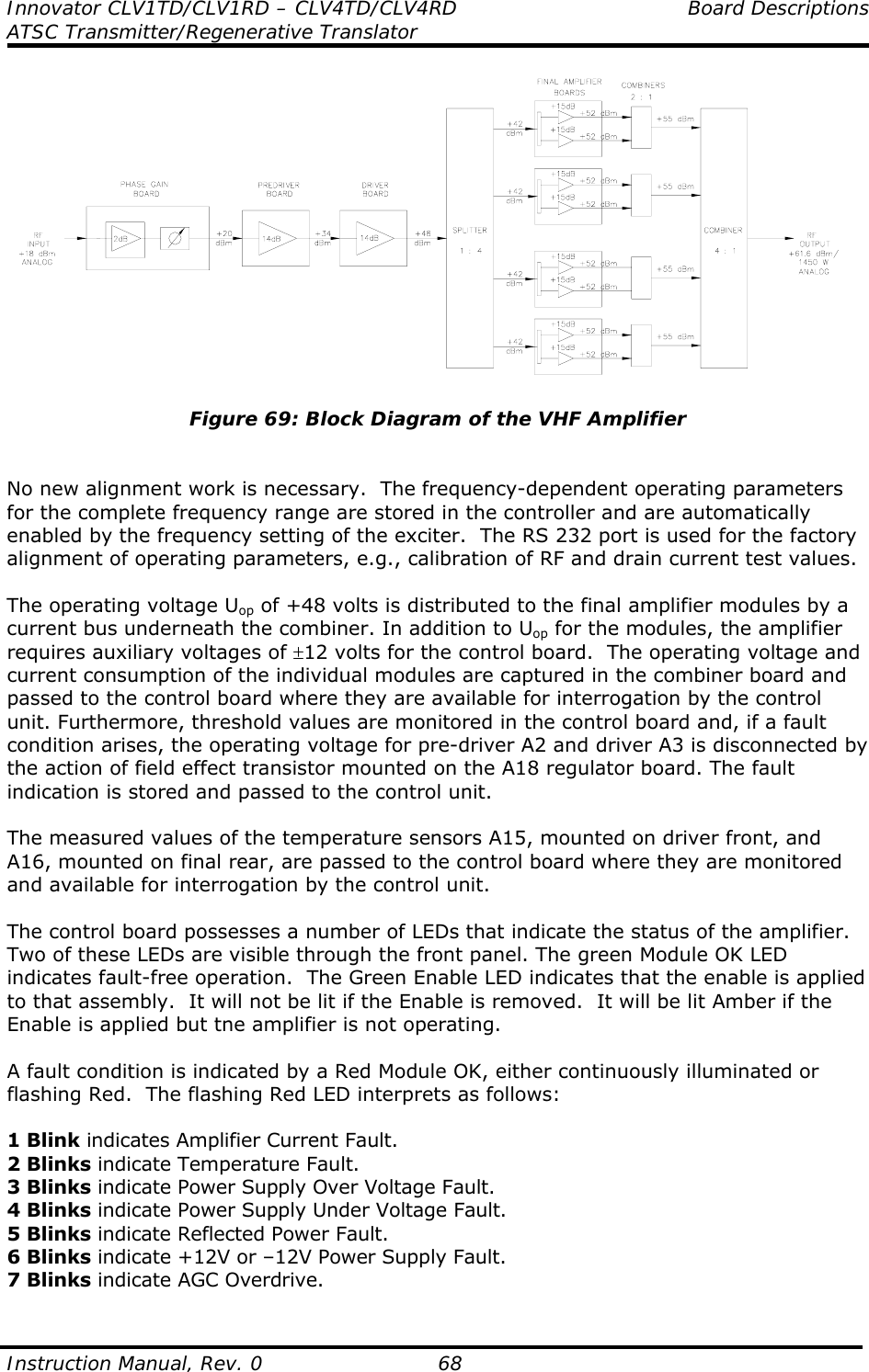
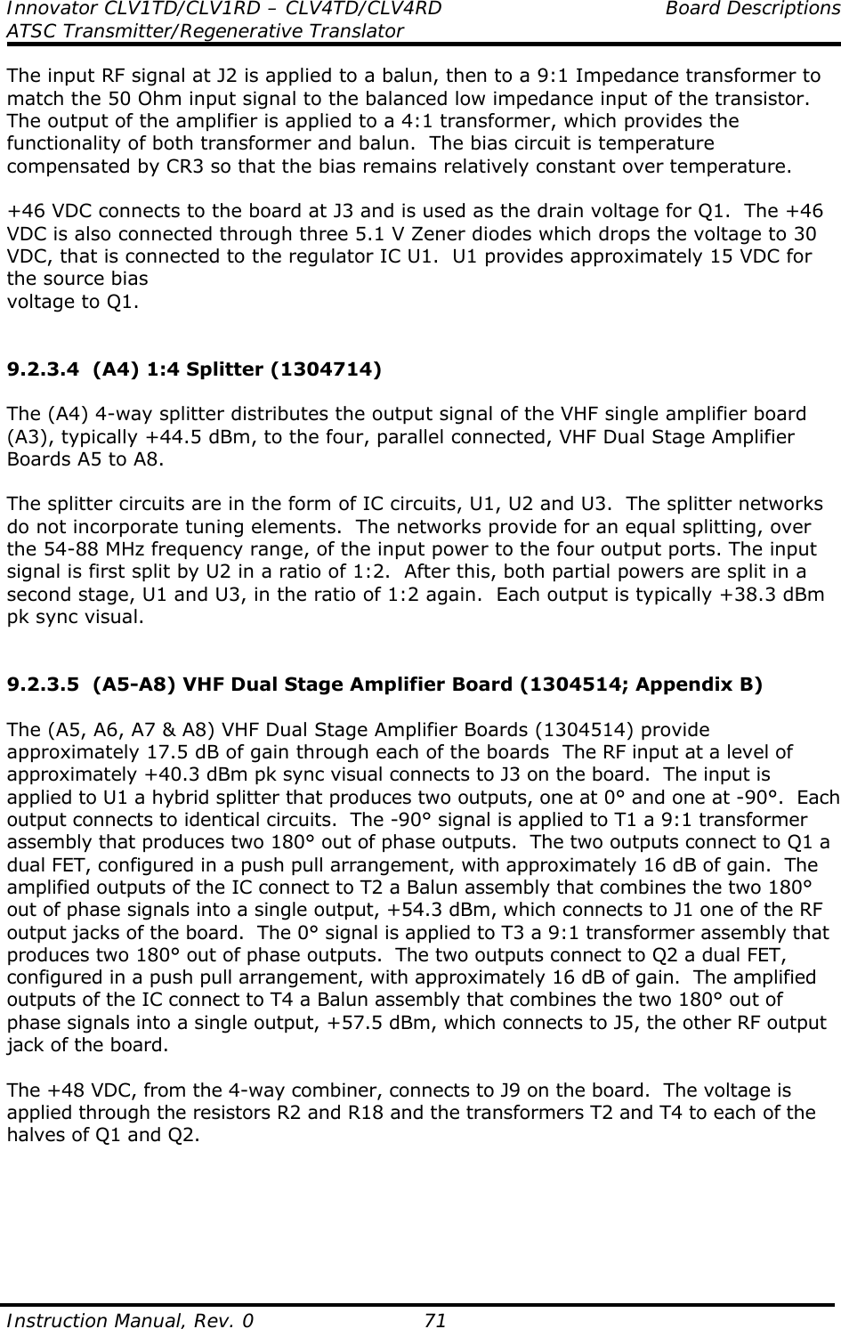
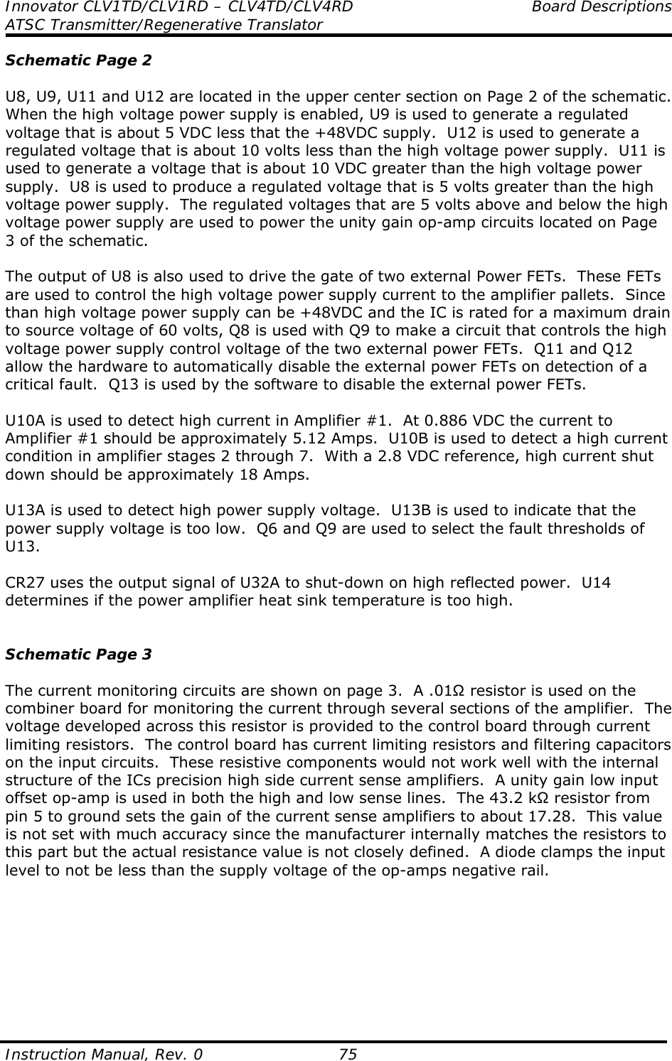
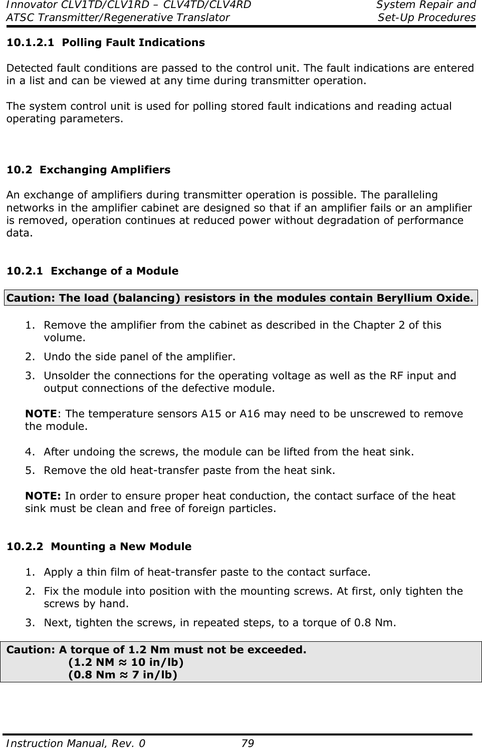
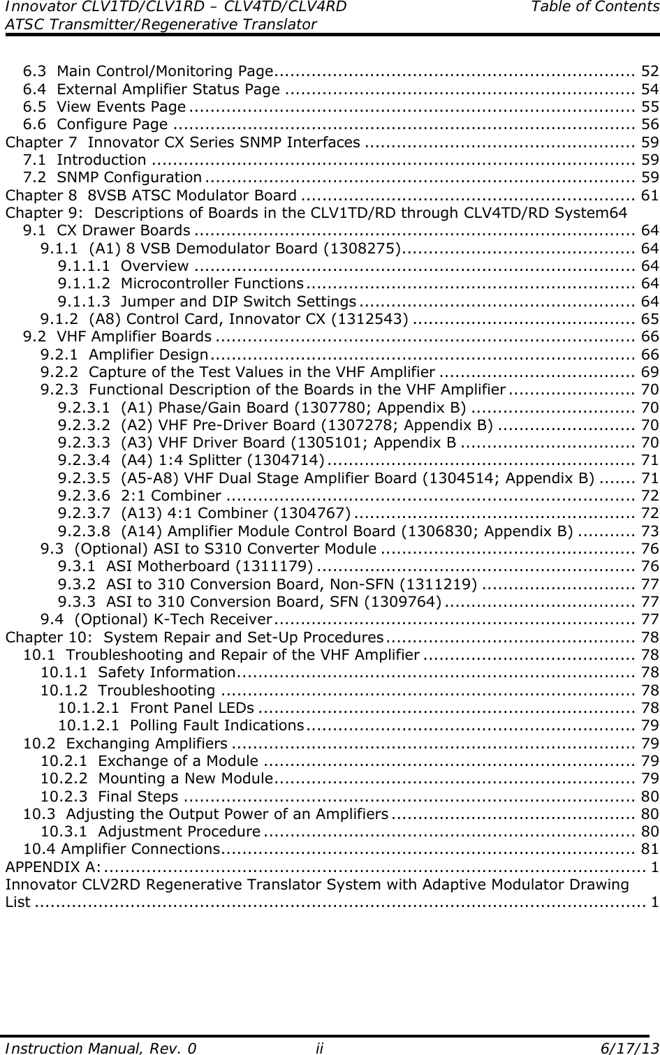
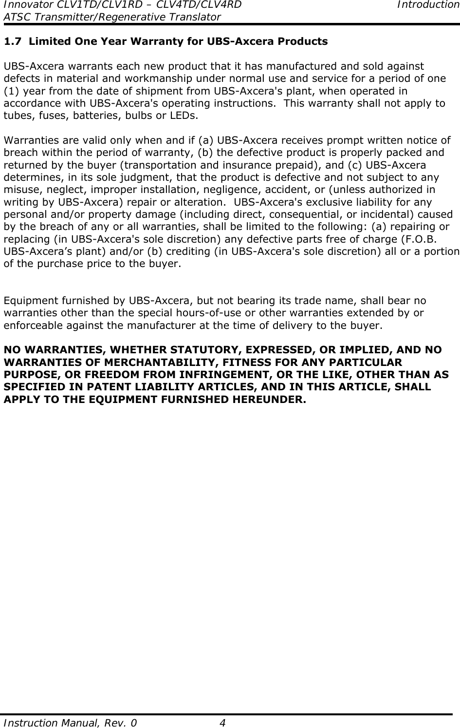
![Innovator CLV1TD/CLV1RD – CLV4TD/CLV4RD Initial On Site ATSC Transmitter/Regenerative Translator Turn On Procedure Instruction Manual, Rev. 0 36 LED Color Description Green System is in Operate mode. OPR/STBY Amber System is in Standby mode. Green CX drawer is functioning normally. Red (blinking) CX drawer Event (fault) is present. Amber CX drawer Event (Fault) occurred, but the CX drawer is now operating normally. STATUS Amber (blinking) CX drawer MPEG input set to internal source (with no Events [Faults]). Table 9: CX Drawer LED Indicators 5.2 Vertical Amplifier Drawer Figure 12: Front View Vertical Amplifier Drawer Pushbutton Function DISABLE Disables or enables the power amplifier. Table 10: Power Amplifier Pushbutton Function Pushbutton Color Description OFF Power amplifier is in Operate mode. DISABLE Red Power amplifier is in Standby mode. Table 11: Power Amplifier Pushbutton Color Indicators Monitor Disable ButtonStatus LEDEnabled LED](https://usermanual.wiki/UBS-Axcera/CLV2TD-4/User-Guide-2052672-Page-41.png)