UBS Axcera CU0TD-5-UBS 200W UHF Digital Transmitter User Manual
UBS-Axcera 200W UHF Digital Transmitter Users Manual
UserManual.wiki
>
UBS Axcera
>
CU0TD 5 UBS User Manual
Users Manual
Navigation menu
Upload a User Manual
Namespaces
Wiki Guide
HTML
PDF
Info
Views
User Manual
Discussion / Help
Navigation
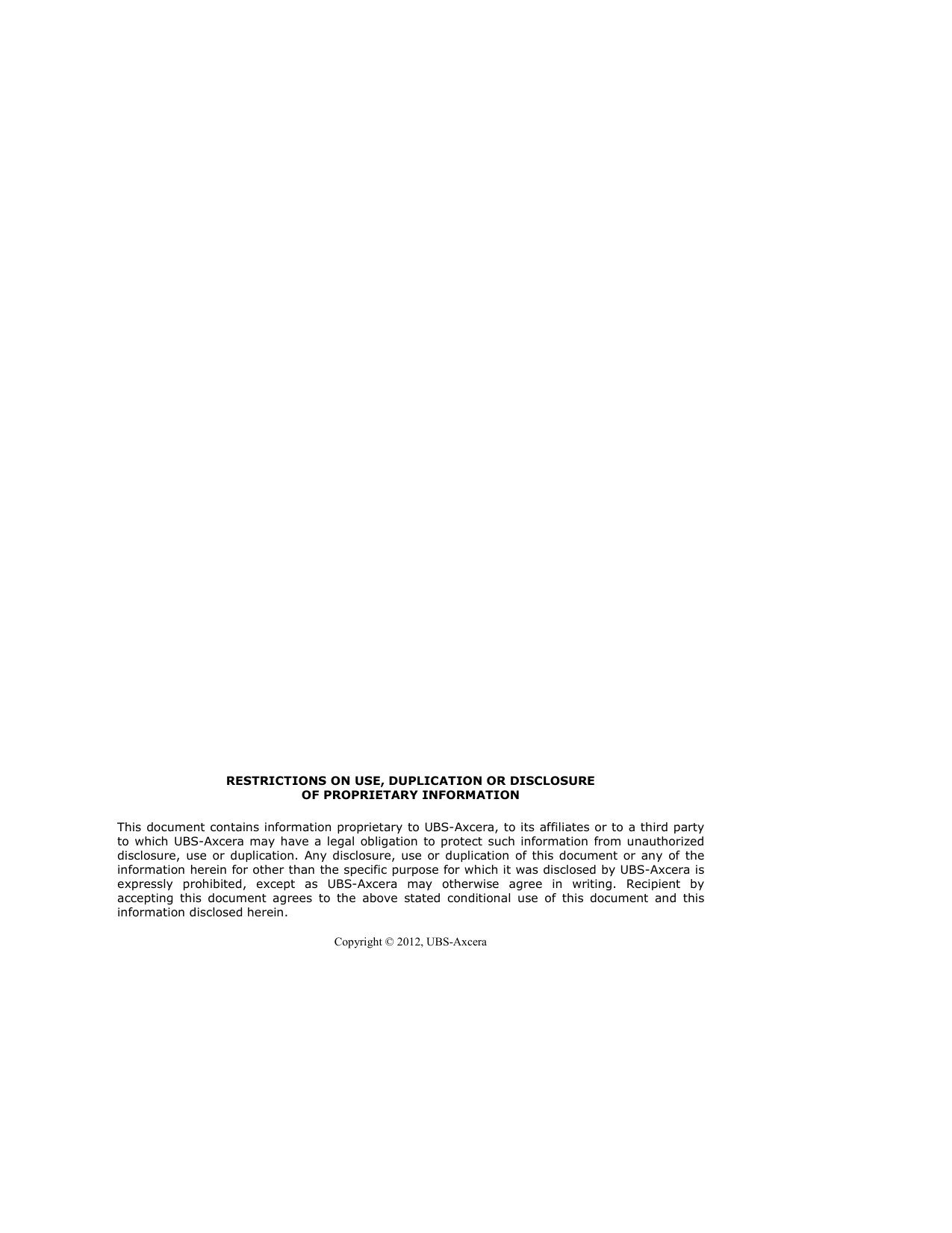
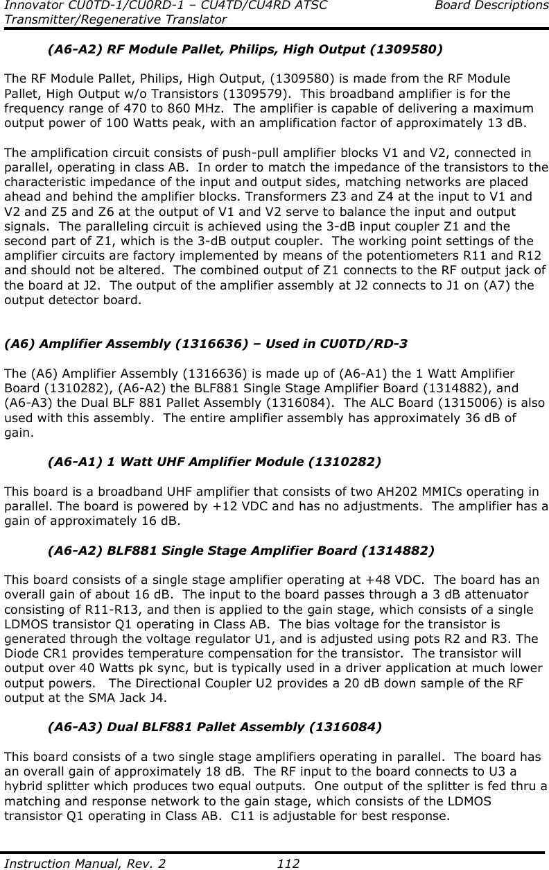
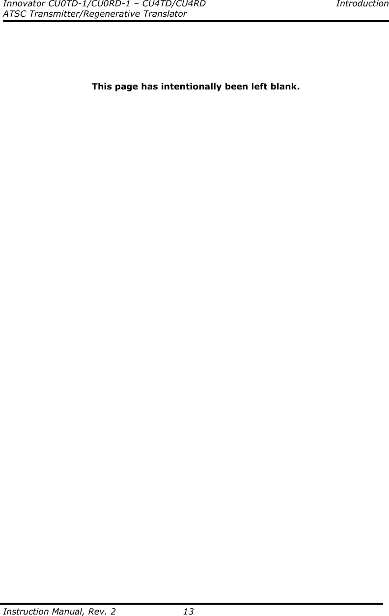
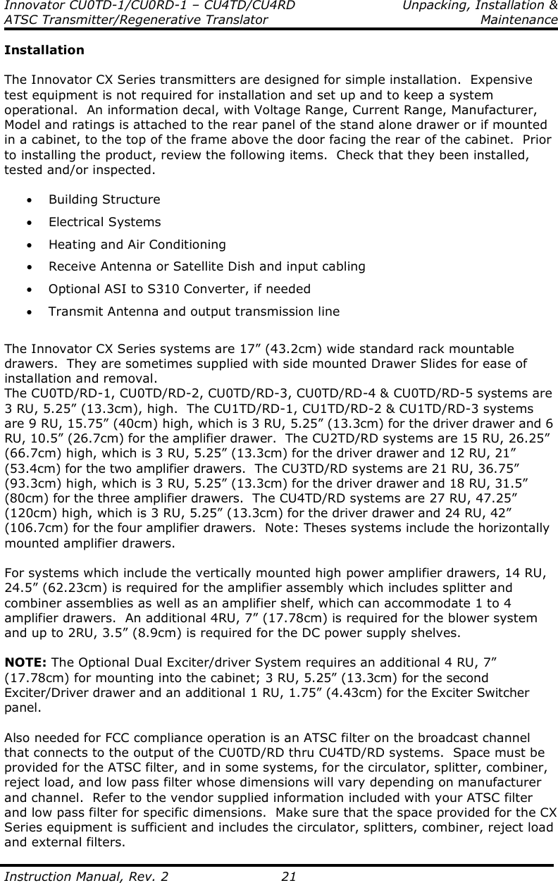
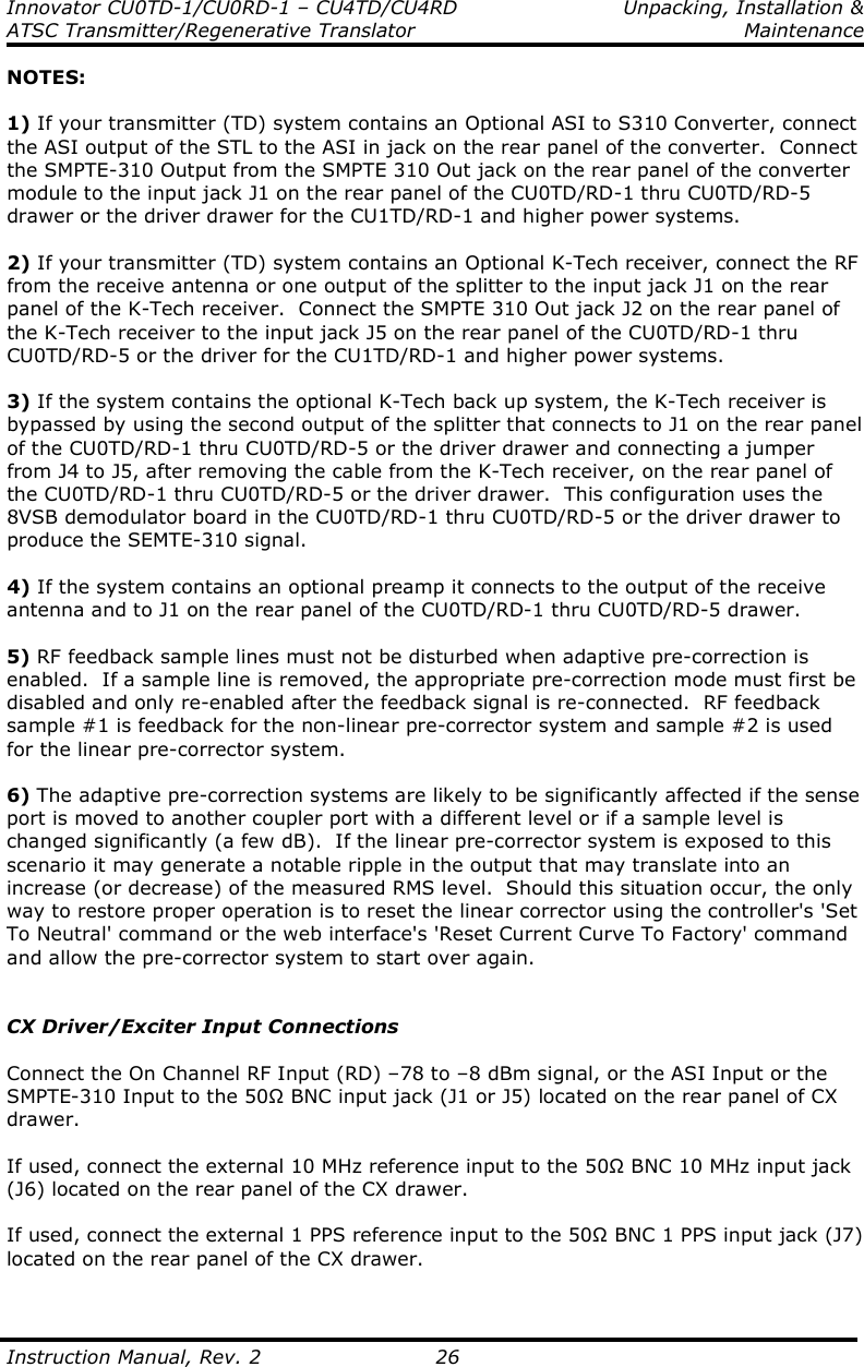
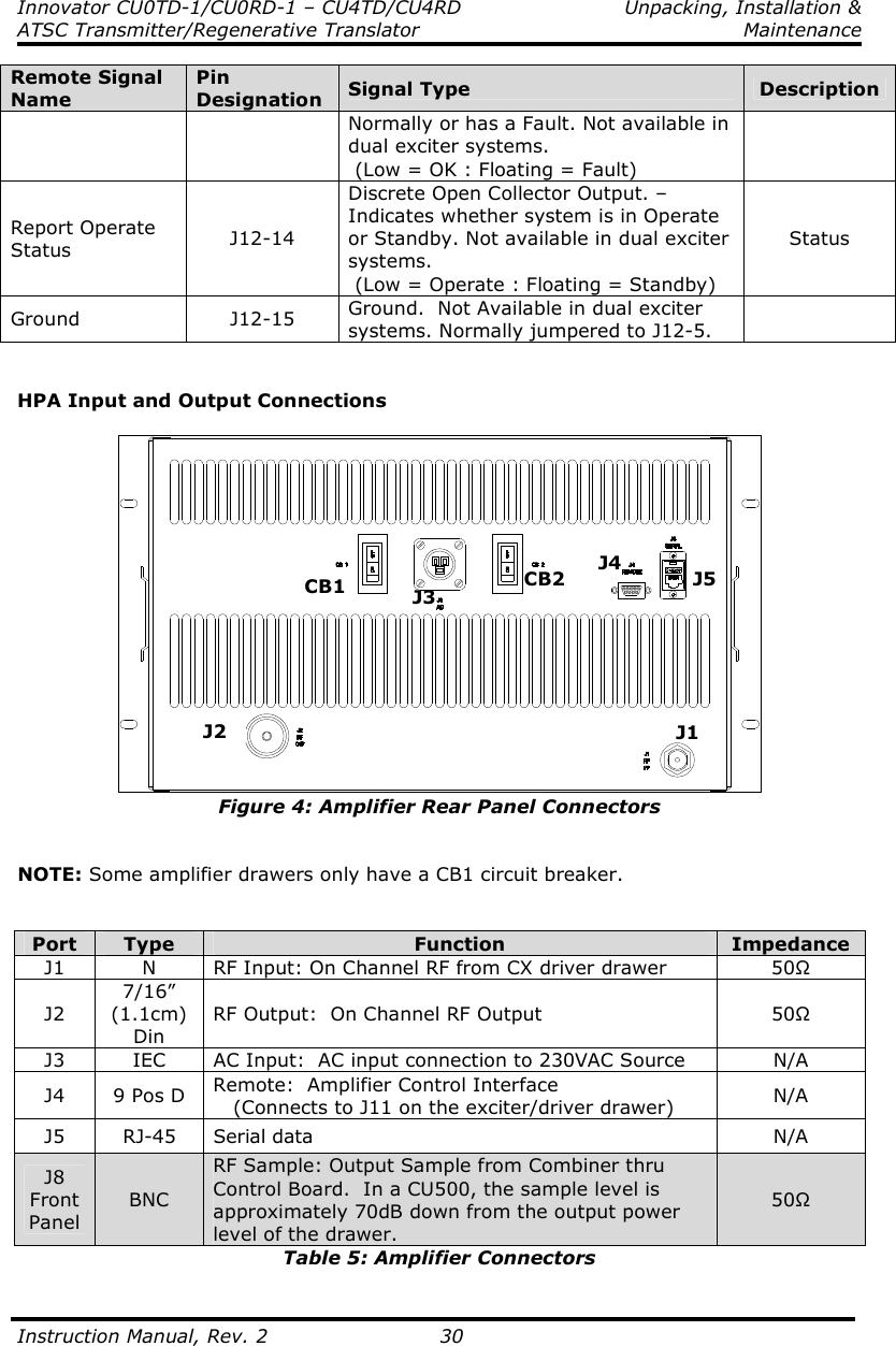
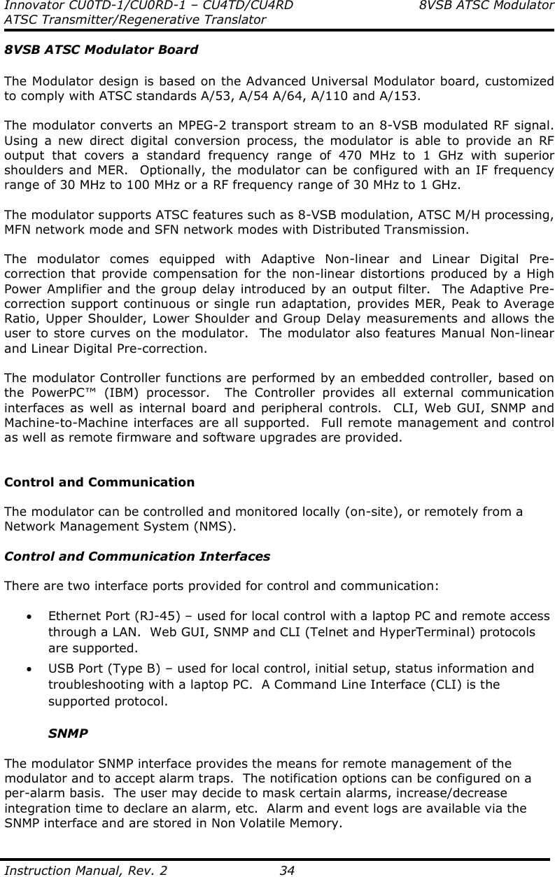
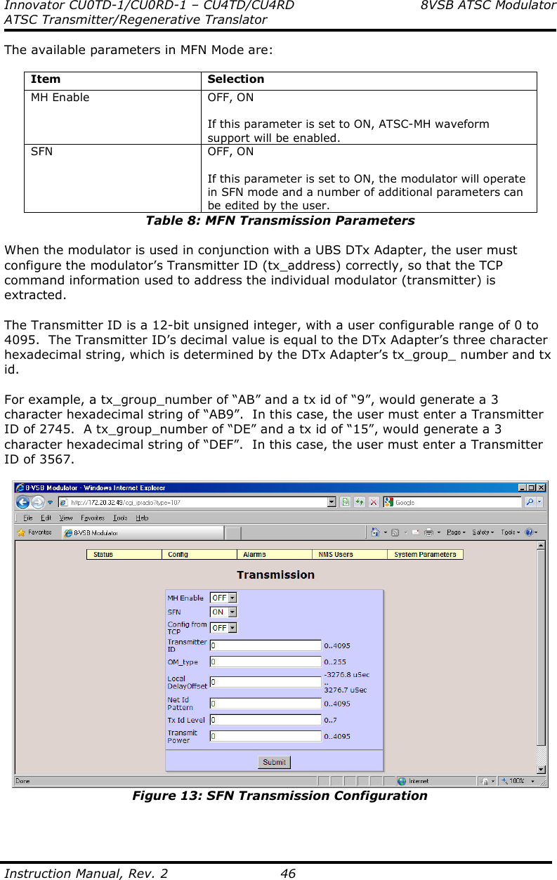
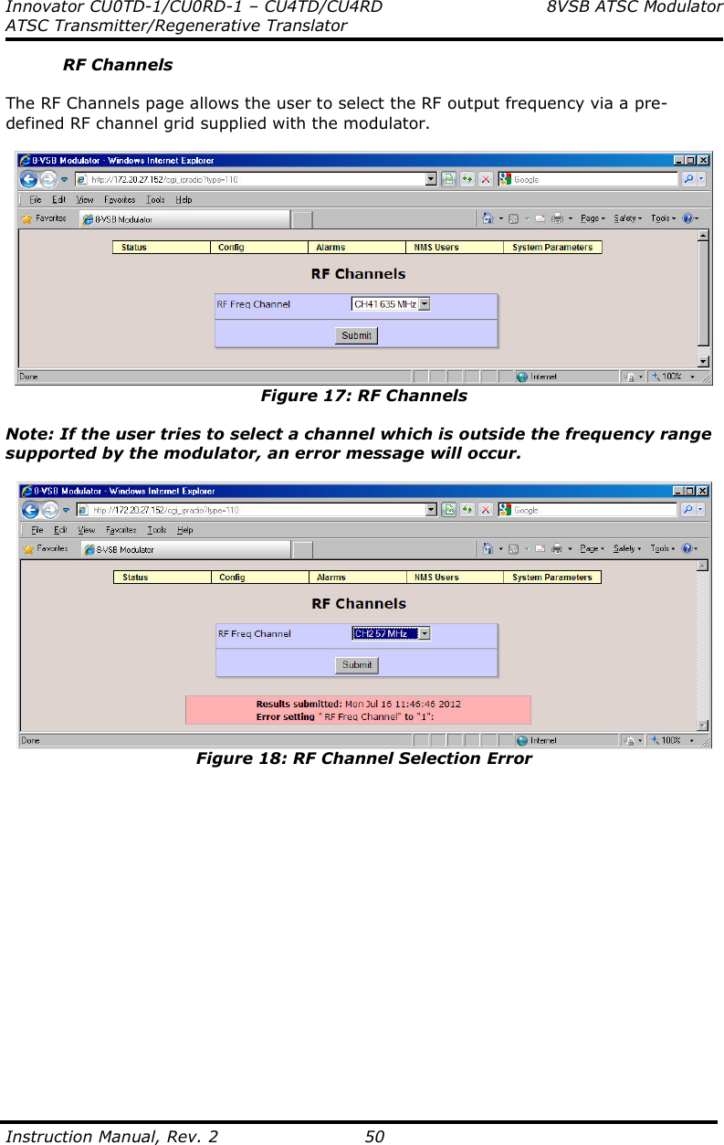
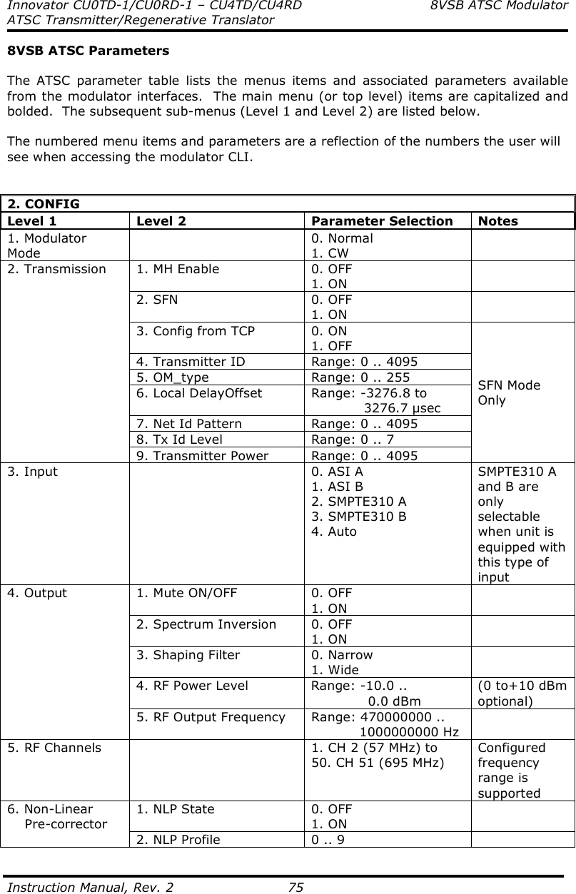
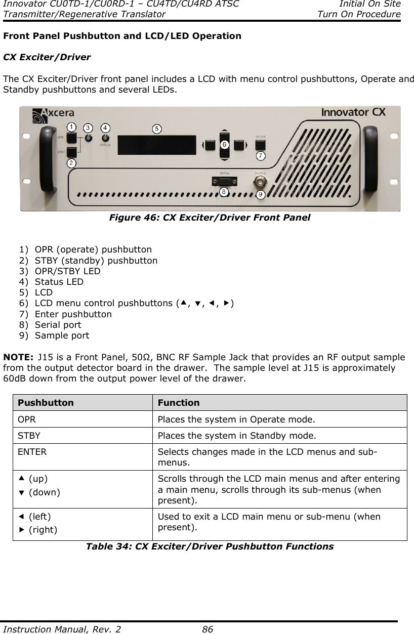
![Innovator CU0TD-1/CU0RD-1 – CU4TD/CU4RD Introduction ATSC Transmitter/Regenerative Translator Instruction Manual, Rev. 2 8 dBm, dBw, dBmV, dBµµµµV, & VOLTAGE EXPRESSED IN WATTS 50 Ohm System WATTS PREFIX dBm dBw dBmV dBµV VOLTAGE 1,000,000,000,000 1 TERAWATT +150 +120 100,000,000,000 100 GIGAWATTS +140 +110 10,000,000,000 10 GIGAWATTS +130 +100 1,000,000,000 1 GIGAWATT +120 + 99 100,000,000 100 MEGAWATTS +110 + 80 10,000,000 10 MEGAWATTS +100 + 70 1,000,000 1 MEGAWATT + 90 + 60 100,000 100 KILOWATTS + 80 + 50 10,000 10 KILOWATTS + 70 + 40 1,000 1 KILOWATT + 60 + 30 100 1 HECTROWATT + 50 + 20 50 + 47 + 17 20 + 43 + 13 10 1 DECAWATT + 40 + 10 1 1 WATT + 30 0 + 77 +137 7.07V 0.1 1 DECIWATT + 20 - 10 + 67 +127 2.24V 0.01 1 CENTIWATT + 10 - 20 + 57 +117 0.707V 0.001 1 MILLIWATT 0 - 30 + 47 +107 224mV 0.0001 100 MICROWATTS - 10 - 40 0.00001 10 MICROWATTS - 20 - 50 0.000001 1 MICROWATT - 30 - 60 0.0000001 100 NANOWATTS - 40 - 70 0.00000001 10 NANOWATTS - 50 - 80 0.000000001 1 NANOWATT - 60 - 90 0.0000000001 100 PICOWATTS - 70 -100 0.00000000001 10 PICOWATTS - 80 -110 0.000000000001 1 PICOWATT - 90 -120 TEMPERATURE CONVERSION °°°°F = 32 + [(9/5) °°°°C] °°°°C = [(5/9) (°°°°F - 32)]](https://usermanual.wiki/UBS-Axcera/CU0TD-5-UBS/User-Guide-1914255-Page-15.png)
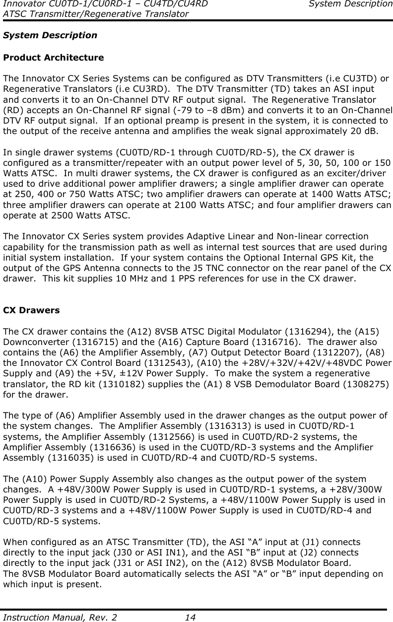

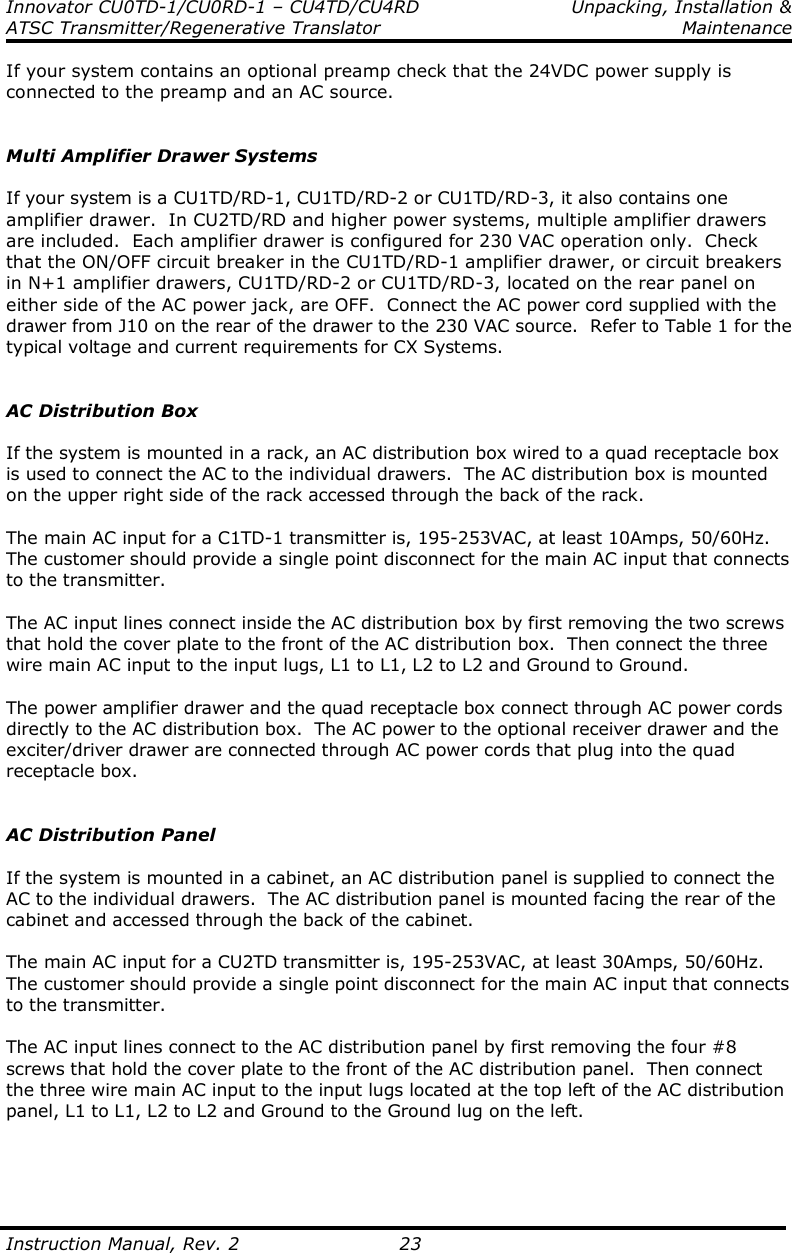
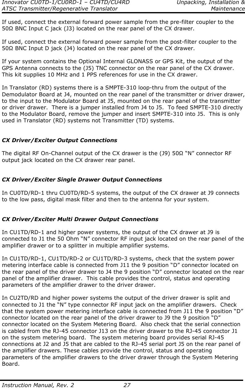
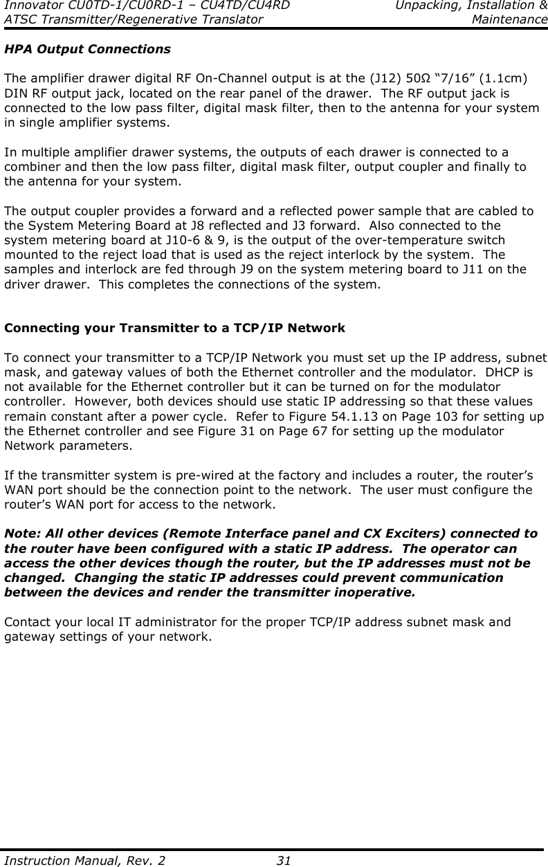
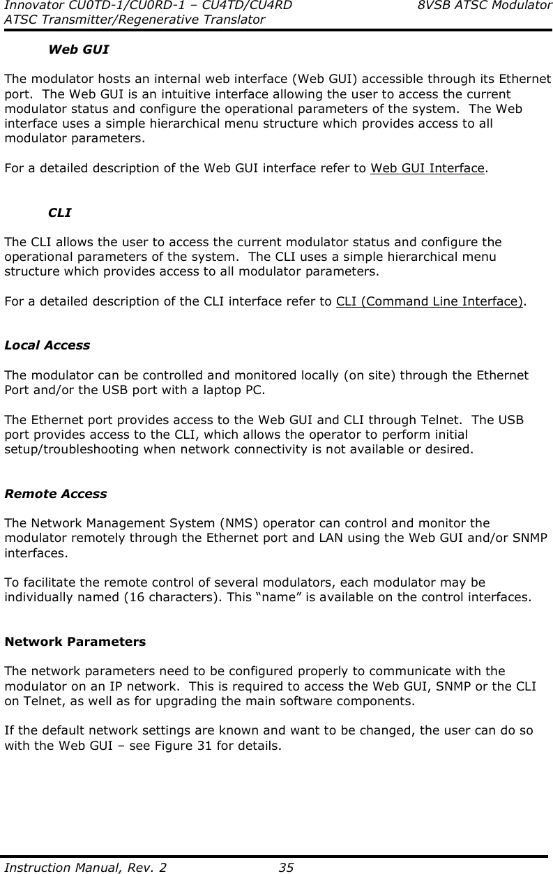
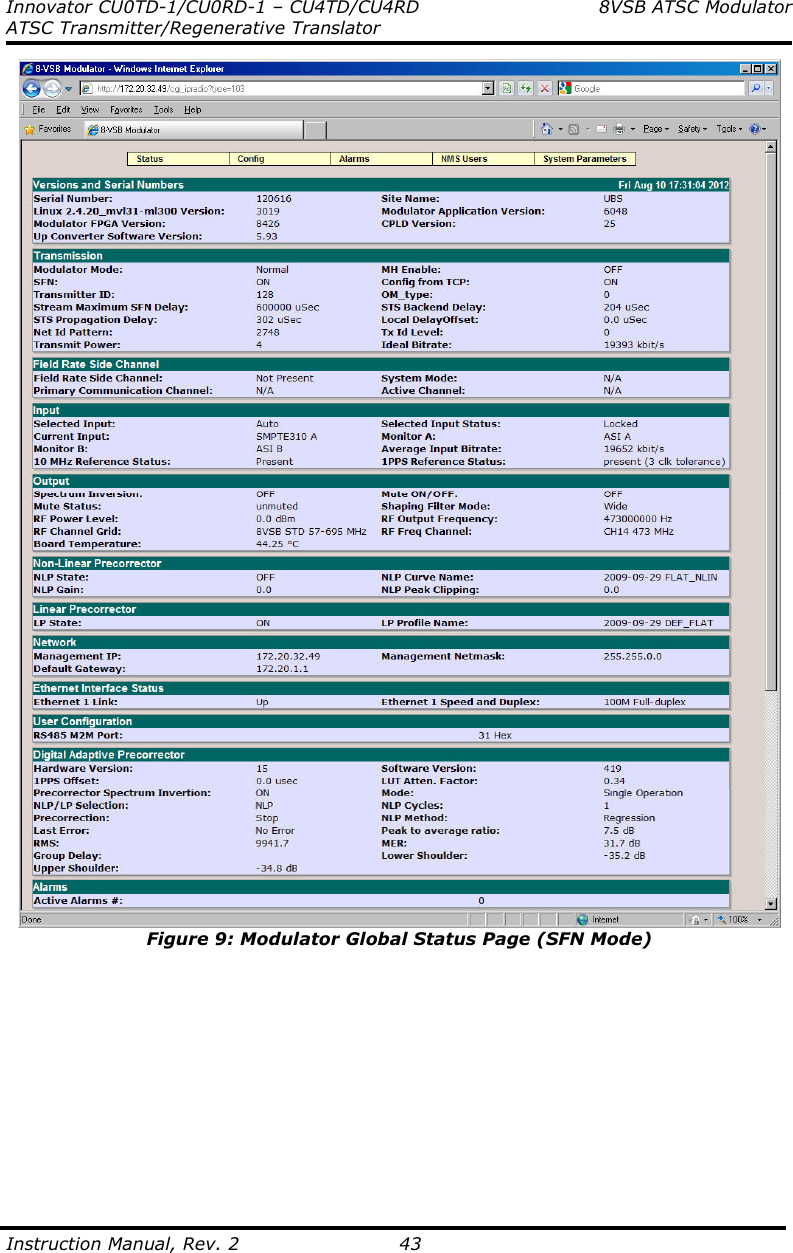
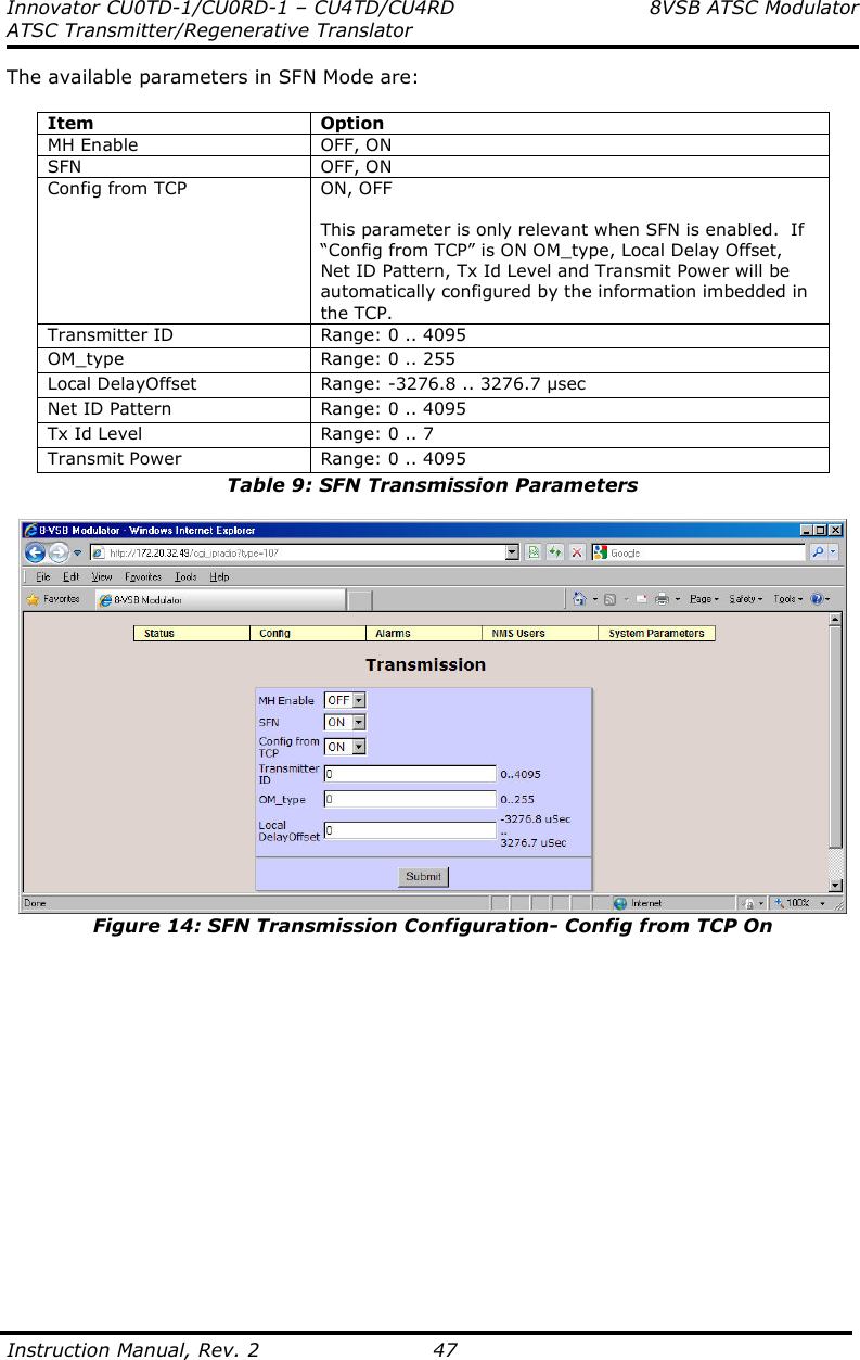
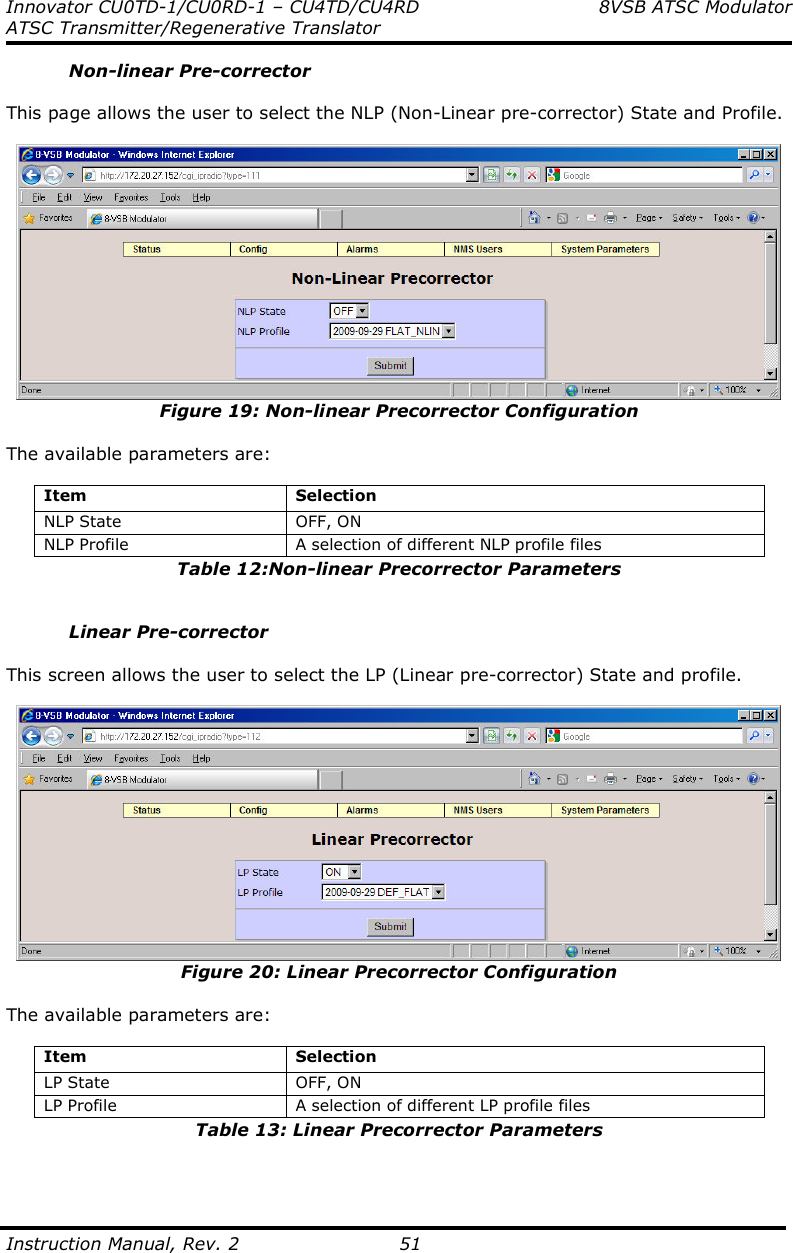
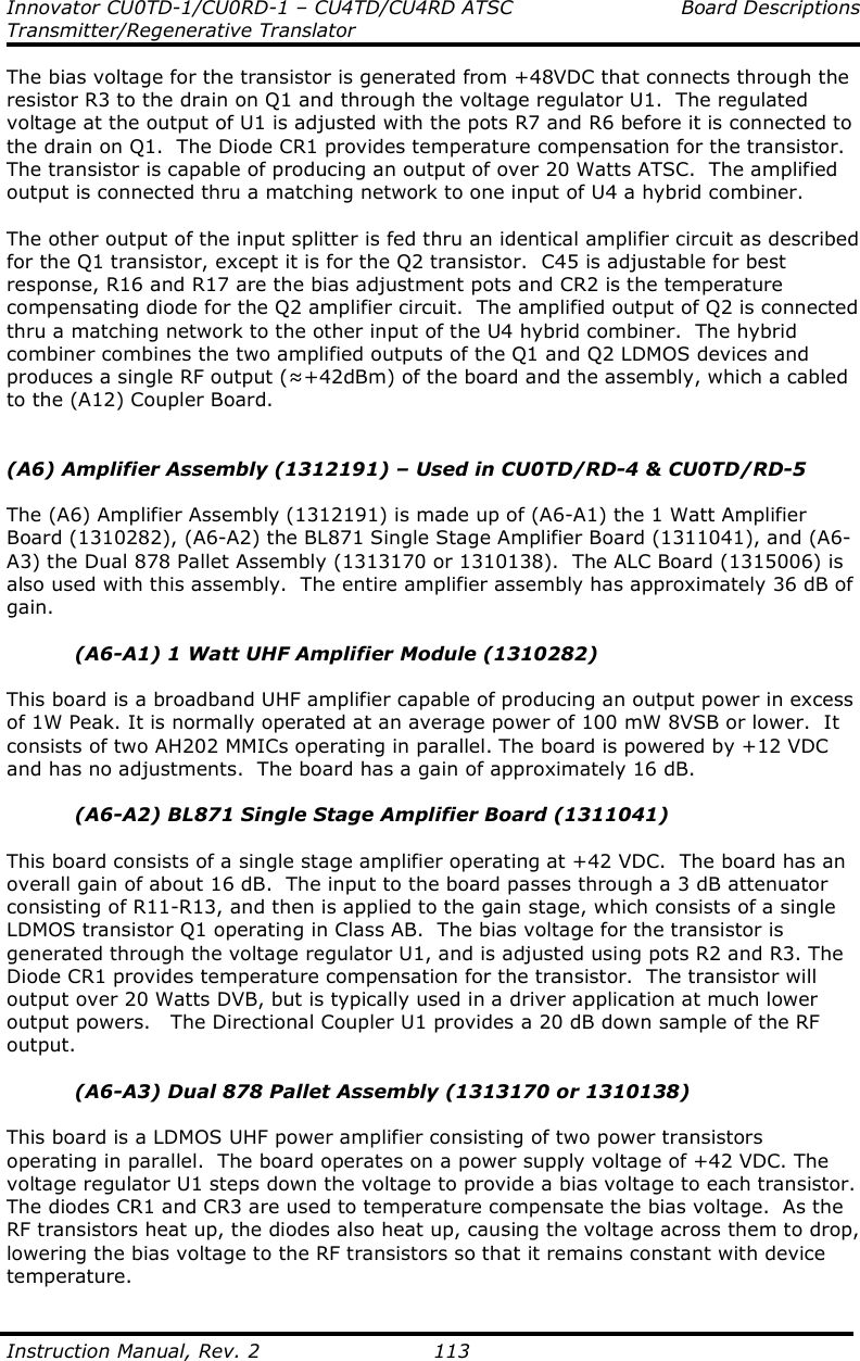
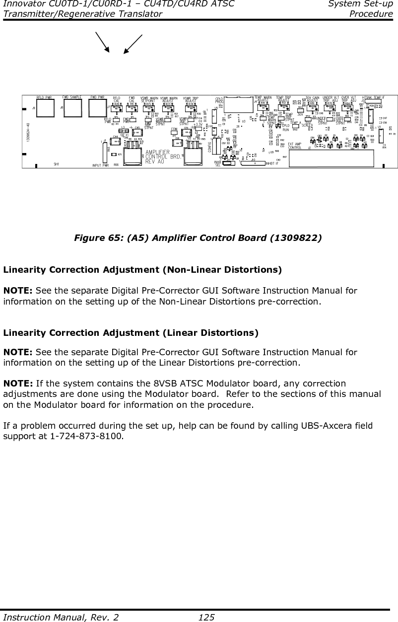
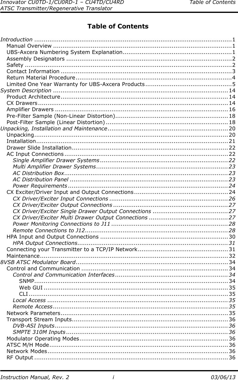
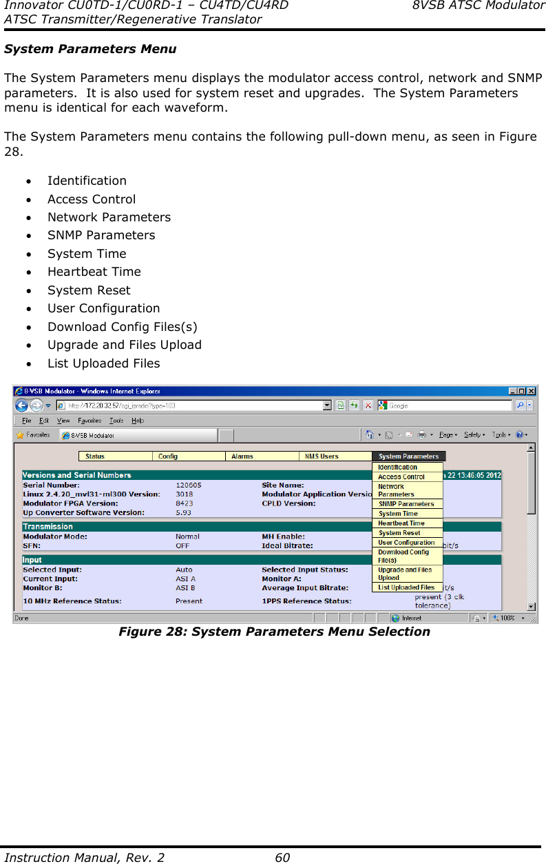
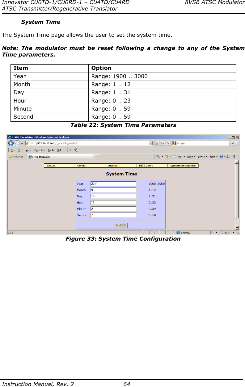
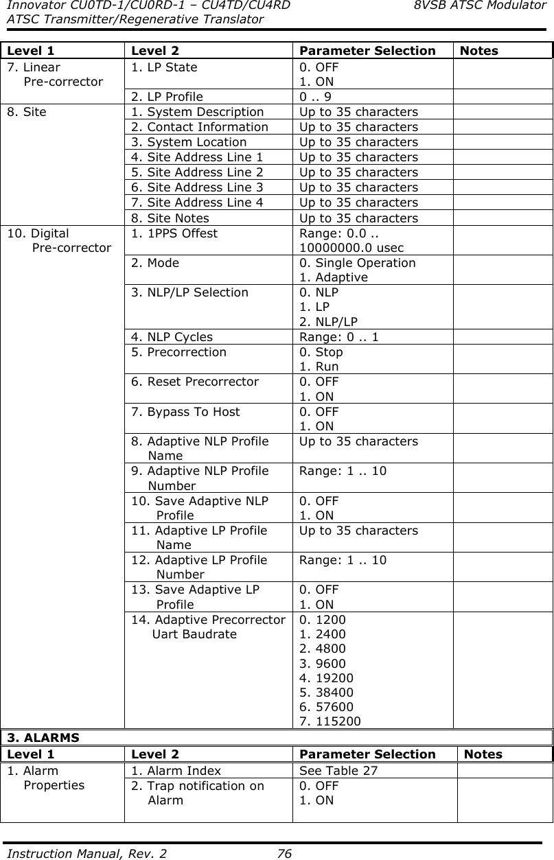
![Innovator CU0TD-1/CU0RD-1 – CU4TD/CU4RD 8VSB ATSC Modulator ATSC Transmitter/Regenerative Translator Instruction Manual, Rev. 2 54 Item Selection NLP Method Legacy, RLS, Regression Used to select Pre-correction algorithm. NLP Cycles Range: 1 .. 10 Ratio of NLP cycles to LP cycles. “X” number of NLP cycles will run before one LP cycle is run. Precorrection Stop, Run Used to Run or Stop the cycles (adaptation processes). Note: Pre-correction is not disabled when the cycles are stopped. Reset Precorector OFF, ON Used to clear the NLP and LP coefficients. Bypass To Host OFF, ON Parameter is only set to ON if the Digital Pre-corrector is controlled using the PC GUI application. Adaptive NLP Profile Name Up to 35 alphanumeric characters Adaptive NLP Profile Number Range: 1 .. 10 Save Adaptive NLP Profile OFF, ON Set to ON, to save curve to memory. Profile name and number should be entered before saving. Adaptive LP Profile Name Up to 35 alphanumeric characters Adaptive LP Profile Number Range: 1 .. 10 Save Adaptive LP Profile OFF, ON Set to ON, to save curve to memory. Profile name and number should be entered before saving. Table 14: Digital Precorrector Parameters Note: If the user would like to use the Adaptive Pre-corrector PC GUI, several parameters must be configured via the Web GUI (or CLI) before communication between the modulator and Adaptive Pre-corrector GUI can be established. The user must set the “Bypass To Host” parameter to “ON” and the “Precorrection” parameter to “Stop”. UART Baudrate Note: The UART Baudrate page is reserved for factory configuration and should not be modified by the user. Comment [M1]: Added text](https://usermanual.wiki/UBS-Axcera/CU0TD-5-UBS/User-Guide-1914255-Page-61.png)
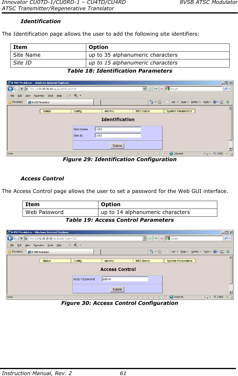
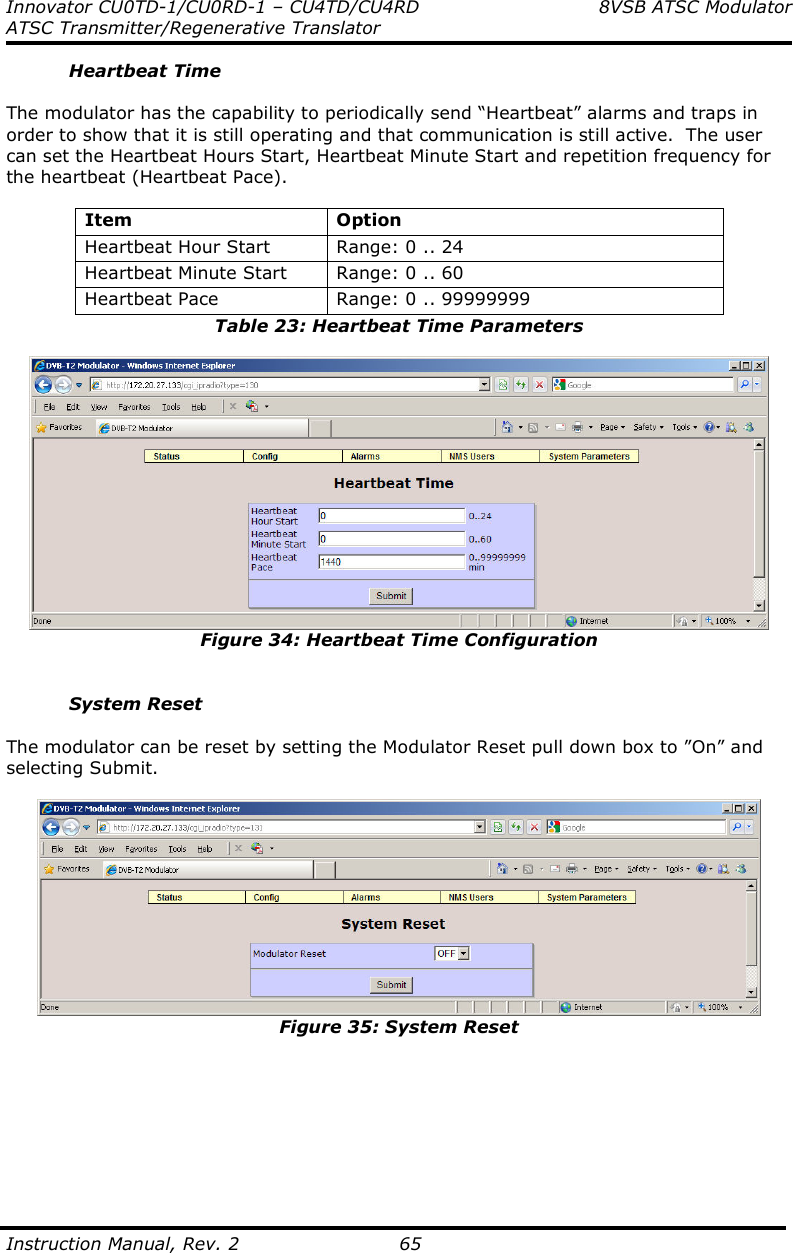
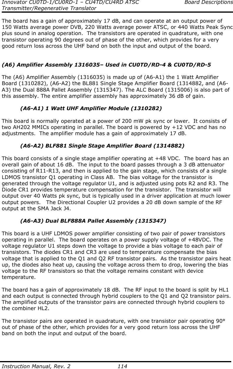
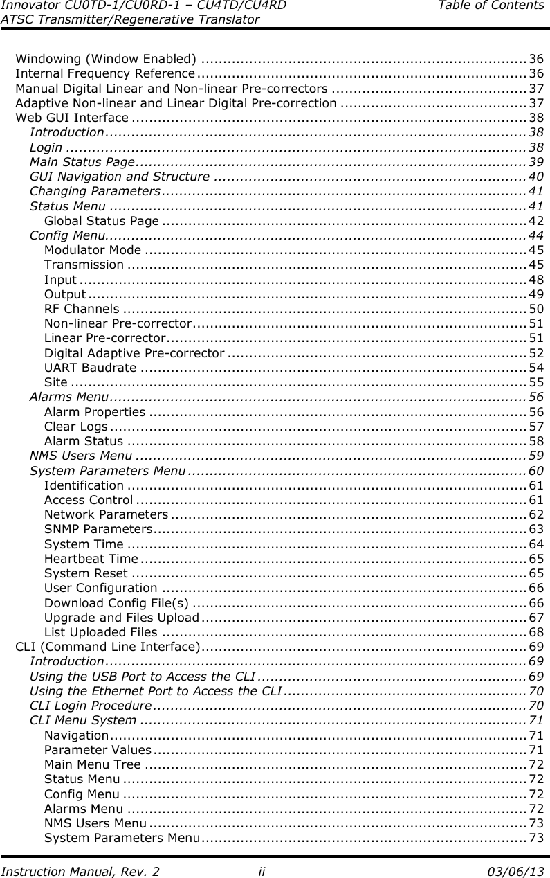
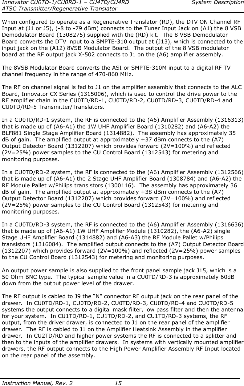
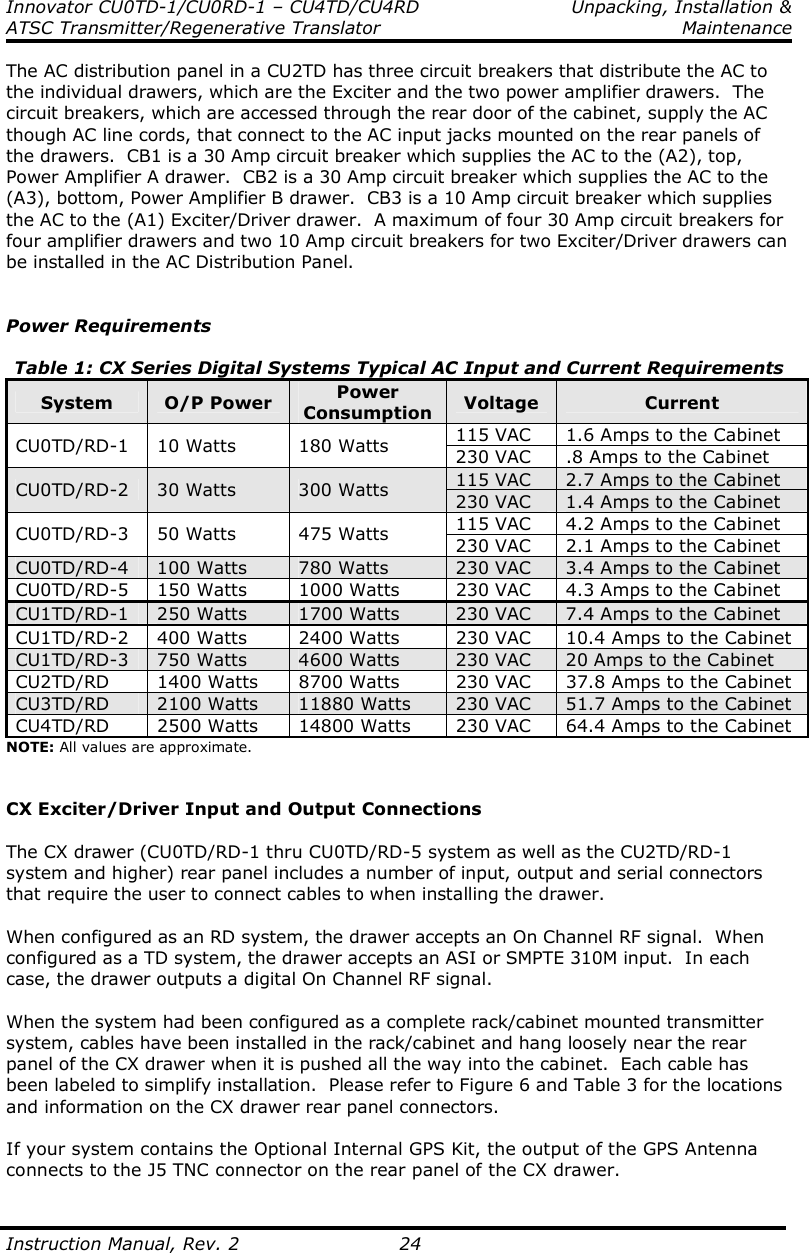
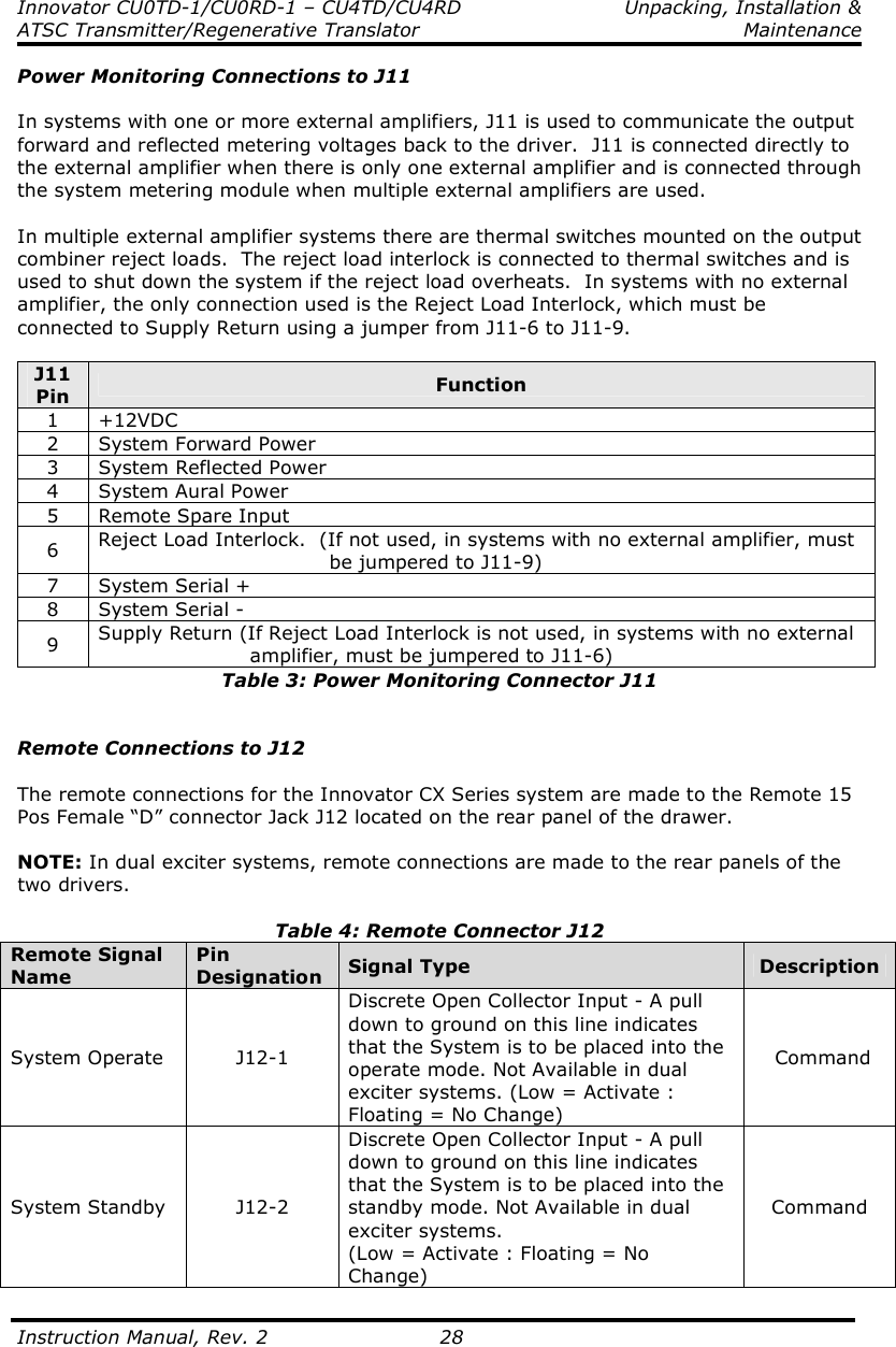
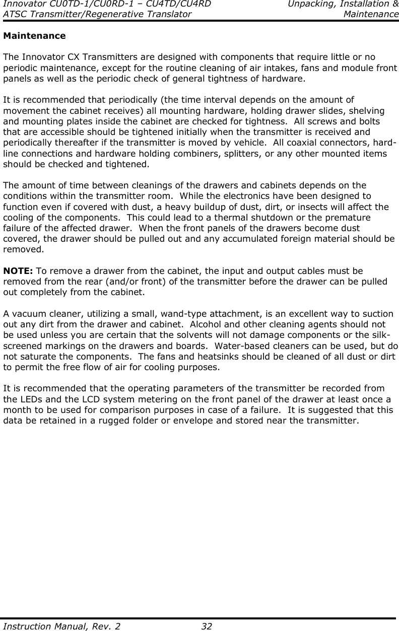
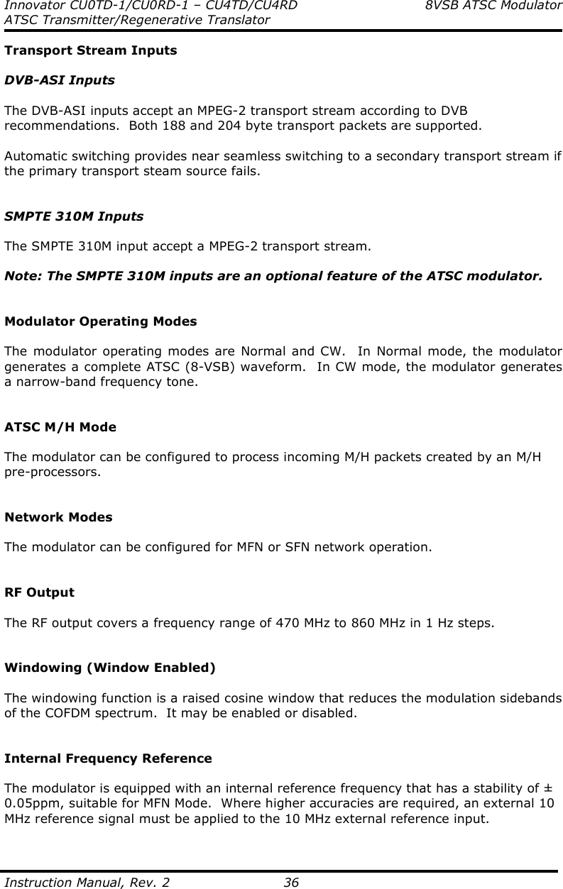
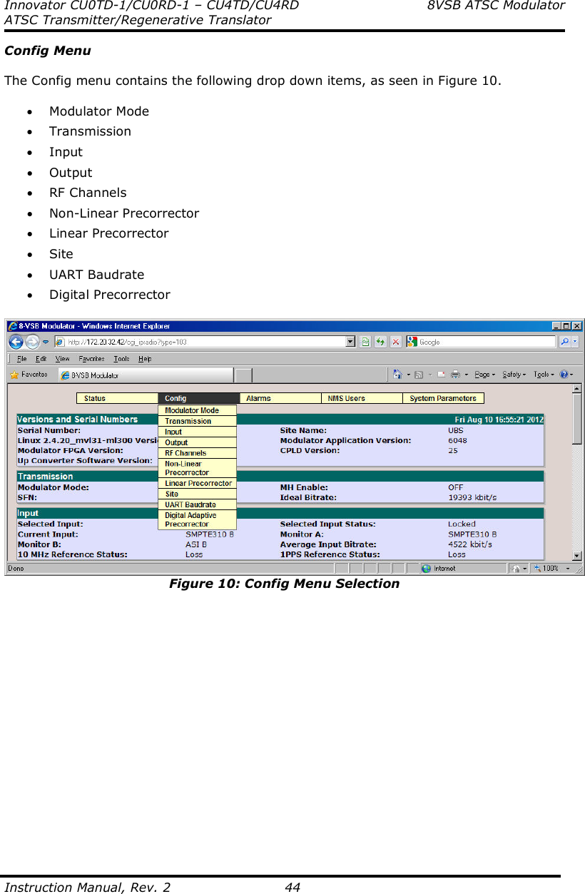
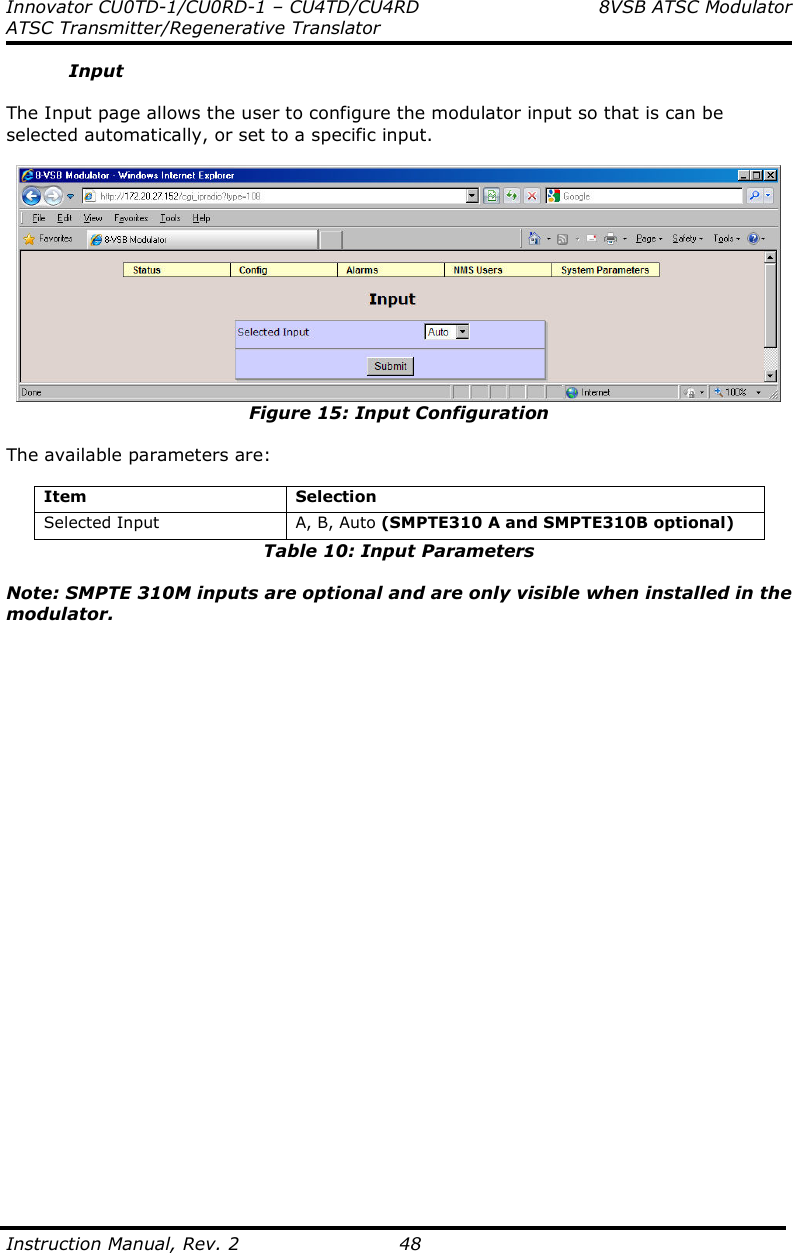
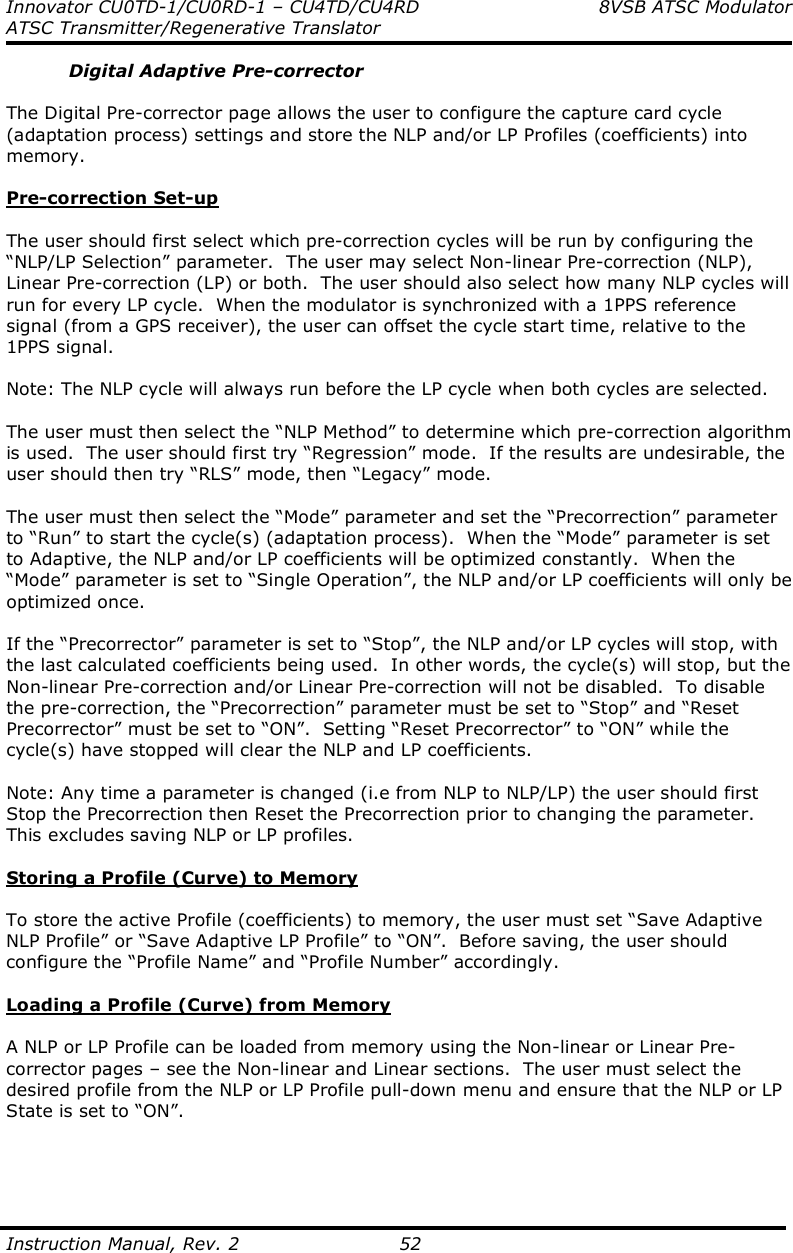
![Innovator CU0TD-1/CU0RD-1 – CU4TD/CU4RD ATSC Initial On Site Transmitter/Regenerative Translator Turn On Procedure Instruction Manual, Rev. 2 87 LED Color Description Green System is in Operate mode. OPR/STBY Amber System is in Standby mode. Green CX drawer is functioning normally. Red (blinking) CX drawer Event (fault) is present. Amber CX drawer Event (Fault) occurred, but the CX drawer is now operating normally. STATUS Amber (blinking) CX drawer MPEG input set to internal source (with no Events [Faults]). Table 35: CX Exciter/Driver LED Indicators High Power Amplifier Figure 47: High Power Amplifier LED Color Description Green System is in Operate mode and operating normally. ENABLE Amber System is in Standby mode. Green System is functioning normally with no faults. Red (blinking) A system Event (fault) is present. STATUS Amber A system Event (Fault) occurred, but the system is now operating normally. Jack Function SAMPLE (J6) Typical sample value is 65dB down from the output power level of the drawer. (500 Watts output power = -8dBm sample level) Table 36: High Power Amplifier LED Indicators Enable LED Status LED Sample](https://usermanual.wiki/UBS-Axcera/CU0TD-5-UBS/User-Guide-1914255-Page-94.png)