UBS Axcera CU250ATD 250-Watt UHF Digital Transmitter User Manual CU250ATD Users Manual
UBS-Axcera 250-Watt UHF Digital Transmitter CU250ATD Users Manual
Compiled Users Manual

Preliminary Instruction Manual
CU250ATD
Innovator
250-Watt Transmitter
AXCERA, LLC
103 FREEDOM DRIVE, P.O. Box 525 LAWRENCE, PA 15055-0525 USA
(724) 873-8100 • FAX (724) 873-8105
www.axcera.com • info@axcera.com

Innovator CU250ATD, 250 Watt Transmitter Table of Contents
Instruction Manual, Rev. 0 August 14, 2007
CU250ATD INNOVATOR 250-WATT TRANSMITTER
Introduction ..................................................................................................1
Manual Overview.....................................................................................1
Assembly Designators..............................................................................1
Safety ....................................................................................................1
Contact Information.................................................................................2
Return Material Procedure ........................................................................2
Warranty Information...............................................................................3
30W Driver Tray Description .........................................................................10
8 VSB Demodulator Board ......................................................................10
8 VSB Modulator Board ..........................................................................10
Amplifier Assembly ................................................................................11
2 Stage UHF Amplifier Board, ...........................................................12
RF Module Pallet w/Philips Transistors ...............................................12
Output Detector Board ...........................................................................12
30W Driver Tray Power Supplies .............................................................13
30W Driver Tray LCD Display and Front Panel LED Indicators ...........................13
30W Driver Tray Input and Output Connections...............................................14
30W Driver Tray Remote Connections ............................................................14
Front Panel Screens for the Transmitter..........................................................16
250W Power Amplifier Tray Description ..........................................................19
2-W ay Splitter ......................................................................................19
600W PEP RF Pallet................................................................................19
2-Way Combiner ...................................................................................19
Amplifier Control Board ..........................................................................19
+12VDC Switching Power Supply ............................................................19
+30VDC Switching Power Supply ............................................................19
250W Power Amplifier Input and Output Connections.......................................20
System Alignment...................................................................................................21
Set Up of the Output Power of the Transmitter..........................................21
ALC Board Set-Up in the Transmitter .......................................................21
Linearity Correction Adjustment ..............................................................22
Frequency Response Delay Equalization Adjustment..................................22
Appendix A
Drawings List..............................................................................................A-1
Transmitter Specifications............................................................................B-1
Innovator CU250ATD, 250 Watt Transmitter Introduction
Instruction Manual, Rev. 0 1
Manual Overview
This manual describes the transmitter, along with the setup and alignment procedures
for the transmitter.
Assembly Designators
Axcera has assigned assembly numbers, Ax designations such as A1, where x=1,2,3…etc,
to all assemblies, modules, and boards in the system. These designations are referenced
in the text of this manual and shown on the block diagram and interconnect drawings
provided in the appendix.
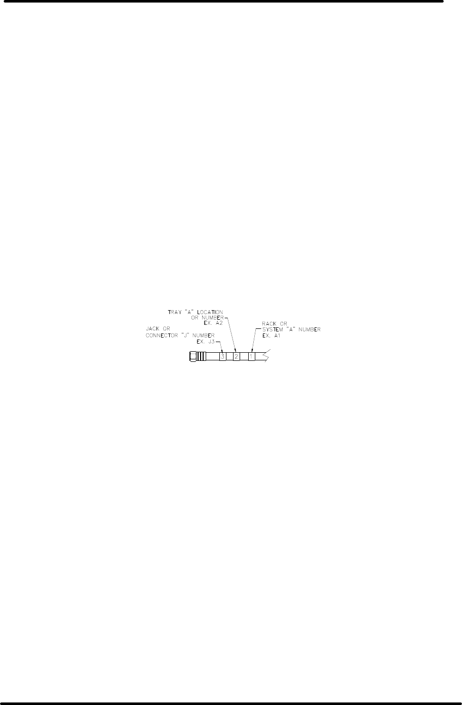
The cables that connect between the boards within a tray or assembly and that connect
between the trays, racks and cabinets are labeled using Brady markers. Figure 1 is an
example of a Brady marked cable. There may be as few as two or as many as four
Markers on any one cable. These Brady markers are read starting furthest from the
connector. If there are four Brady Markers, this marker is the transmitter number such
as transmitter 1 or transmitter 2. The next or the furthest Brady Marker is the rack or
cabinet number on an interconnect cable or the board number within a tray. The next
number on an interconnect cable is the Tray location or number. The Brady marker
closest to the connector is the jack or connector number on an interconnect cable or the
jack or connector number on the board within a tray.
Figure 1: Brady Marker Identification
Drawing
Safety
The transmitter systems manufactured by Axcera are designed to be easy to use and
repair while providing protection from electrical and mechanical hazards. Please review
the following warnings and familiarize yourself with the operation and servicing procedures
before working on the transmitter system.
Read All safety Instructions – All of the safety instructions should be read and
understood before operating this equipment.
Retain Manuals – The manuals for the transmitter should be retained at the transmitter
site for future reference. Axcera provides two manuals for this purpose; one manual can
be left at the office while the other can be kept at the site.
Heed all Notes, Warnings, and Cautions – All of the notes, warnings, and cautions
listed in this safety section and throughout the manual must be followed.
Follow Operating Instructions – All of the operating and use instructions for the
transmitter should be followed.
Cleaning – Unplug or otherwise disconnect all power from the equipment before cleaning.
Do not use liquid or aerosol cleaners. Use a damp cloth for cleaning.

Innovator CU250ATD, 250 Watt Transmitter Introduction
Instruction Manual, Rev. 0 2
Ventilation – Openings in the cabinet and module front panels are provided for
ventilation. To ensure the reliable operation of the driver/transmitter, and to protect the
unit from overheating, these openings must not be blocked.
Servicing – Do not attempt to service this product yourself until becoming familiar with
the equipment. If in doubt, refer all servicing questions to qualified Axcera service
personnel.
Replacement Parts – When replacement parts are used, be sure that the parts have the
same functional and performance characteristics as the original part. Unauthorized
substitutions may result in fire, electric shock, or other hazards. Please contact the
Axcera Technical Service Department if you have any questions regarding service or
replacement parts.
Contact Information
The Axcera Field Service Department can be contacted by phone at (724) 873-8100 or
by fax at (724) 873-8105.
Before calling Axcera, please be prepared to supply the Axcera technician with answers to
the following questions. This will save time and help ensure the most direct resolution to
the problem.
1. What are the Customers’ Name and call letters?
2. What are the model number and type of transmitter?
3. Is the transmitter digital or analog?
4. How long has the transmitter been on the air? (Approximately when was the
transmitter installed.)
5. What are the symptoms being exhibited by the transmitter? Include the current
control/power supply LCD readings and the status of LEDs on the front panels of
the modules. If possible, include the control/power supply LCD readings before
the problem occurred.
Return Material Procedure
To insure the efficient handling of equipment or components that have been returned for
repair, Axcera requests that each returned item be accompanied by a Return Material
Authorization Number (RMA#). The RMA# can be obtained from any Axcera Field
Service Engineer by contacting the Axcera Field Service Department at (724) 873-8100
or by fax at (724) 873-8105. This procedure applies to all items sent to the Field
Service Department regardless of whether the item was originally manufactured by
Axcera.
When equipment is sent to the field on loan, an RMA# is included with the unit. The RMA#
is intended to be used when the unit is returned to Axcera. In addition, all shipping
material should be retained for the return of the unit to Axcera.
Replacement assemblies are also sent with an RMA# to allow for the proper routing of the
exchanged hardware. Failure to close out this type of RMA# will normally result in the
customer being invoiced for the value of the loaner item or the exchanged assembly.

Innovator CU250ATD, 250 Watt Transmitter Introduction
Instruction Manual, Rev. 0 3
When shipping an item to Axcera, please include the RMA# on the packing list and on the
shipping container. The packing slip should also include contact information and a brief
description of why the unit is being returned.
Please forward all RMA items to:
AXCERA, LLC
103 Freedom Drive
P.O. Box 525
Lawrence, PA 15055-0525 USA
For more information concerning this procedure, call the Axcera Field Service Department
at (724) 873-8100.
Axcera can also be contacted through e-mail at info@axcera.com and on the Web at
www.axcera.com.
Limited One Year Warranty for Axcera Products
Axcera warrants each new product that it has manufactured and sold against defects in
material and workmanship under normal use and service for a period of one (1) year
from the date of shipment from Axcera's plant, when operated in accordance with
Axcera's operating instructions. This warranty shall not apply to tubes, fuses, batteries,
bulbs or LEDs.
Warranties are valid only when and if (a) Axcera receives prompt written notice of
breach within the period of warranty, (b) the defective product is properly packed and
returned by the buyer (transportation and insurance prepaid), and (c) Axcera
determines, in its sole judgment, that the product is defective and not subject to any
misuse, neglect, improper installation, negligence, accident, or (unless authorized in
writing by Axcera) repair or alteration. Axcera's exclusive liability for any personal
and/or property damage (including direct, consequential, or incidental) caused by the
breach of any or all warranties, shall be limited to the following: (a) repairing or
replacing (in Axcera's sole discretion) any defective parts free of charge (F.O.B. Axcera’s
plant) and/or (b) crediting (in Axcera's sole discretion) all or a portion of the purchase
price to the buyer.
Equipment furnished by Axcera, but not bearing its trade name, shall bear no warranties
other than the special hours-of-use or other warranties extended by or enforceable
against the manufacturer at the time of delivery to the buyer.
NO WARRANTIES, WHETHER STATUTORY, EXPRESSED, OR IMPLIED, AND NO
WARRANTIES OF MERCHANTABILITY, FITNESS FOR ANY PARTICULAR
PURPOSE, OR FREEDOM FROM INFRINGEMENT, OR THE LIKE, OTHER THAN AS
SPECIFIED IN PATENT LIABILITY ARTICLES, AND IN THIS ARTICLE, SHALL
APPLY TO THE EQUIPMENT FURNISHED HEREUNDER.

Innovator CU250ATD, 250 Watt Transmitter Introduction
Instruction Manual, Rev. 0 4
F WARNING!!!
× HIGH VOLTAGE Ø
DO NOT ATTEMPT TO REPAIR OR TROUBLESHOOT THIS EQUIPMENT UNLESS
YOU ARE FAMILIAR WITH ITS OPERATION AND EXPERIENCED IN
SERVICING HIGH VOLTAGE EQUIPMENT. LETHAL VOLTAGES ARE PRESENT
WHEN POWER IS APPLIED TO THIS SYSTEM. IF POSSIBLE, TURN OFF
POWER BEFORE MAKING ADJUSTMENTS TO THE SYSTEM.
« RADIO FREQUENCY RADIATION HAZARD «
MICROWAVE, RF AMPLIFIERS AND TUBES GENERATE HAZARDOUS RF
RADIATION THAT CAN CAUSE SEVERE INJURY INCLUDING CATARACTS,
WHICH CAN RESULT IN BLINDNESS. SOME CARDIAC PACEMAKERS MAY BE
AFFECTED BY THE RF ENERGY EMITTED BY RF AND MICROWAVE
AMPLIFIERS. NEVER OPERATE THE TRANSMITTER SYSTEM WITHOUT A
PROPERLY MATCHED RF ENERGY ABSORBING LOAD ATTACHED. KEEP
PERSONNEL AWAY FROM OPEN WAVEGUIDES AND ANTENNAS. NEVER
LOOK INTO AN OPEN WAVEGUIDE OR ANTENNA. MONITOR ALL PARTS OF
THE RF SYSTEM FOR RADIATION LEAKAGE AT REGULAR INTERVALS.

Innovator CU250ATD, 250 Watt Transmitter Introduction
Instruction Manual, Rev. 0 5
EMERGENCY FIRST AID INSTRUCTIONS
Personnel engaged in the installation, operation, or maintenance of this equipment are
urged to become familiar with the following rules both in theory and practice. It is the
duty of all operating personnel to be prepared to give adequate Emergency First Aid and
thereby prevent avoidable loss of life.
RESCUE BREATHING
1. Find out if the person is
breathing.
You must find out if the
person has stopped
breathing. If you think he is
not breathing, place him flat
on his back. Put your ear
close to his mouth and look
at his chest. If he is breathing
you can feel the air on your
cheek. You can see his chest
move up and down. If you do
not feel the air or see the
chest move, he is not
breathing.
2. If he is not breathing, open
the airway by tilting his head
backwards.
Lift up his neck with one hand
and push down on his
forehead with the other. This
opens the airway. Sometimes
doing this will let the person
breathe again by himself.
3. If he is still not breathing,
begin rescue breathing.
-Keep his head tilted
backward. Pinch nose shut.
-Put your mouth tightly over
his mouth.
-Blow into his mouth once
every five seconds
-DO NOT STOP rescue
breathing until help arrives.
LOOSEN CLOTHING - KEEP
WARM
Do this when the victim is
breathing by himself or help
is available. Keep him as
quiet as possible and from
becoming chilled. Otherwise
treat him for shock.
BURNS
SKIN REDDENED: Apply ice cold water to
burned area to prevent burn from going
deeper into skin tissue. Cover area with a
clean sheet or cloth to keep away air. Consult
a physician.
SKIN BLISTERED OR FLESH CHARRED:
Apply ice cold water to burned area to
prevent burn from going deeper into skin
tissue.
Cover area with clean sheet or cloth to keep
away air. Treat victim for shock and take to
hospital.
EXTENSIVE BURN - SKIN BROKEN: Cover
area with clean sheet or cloth to keep away
air. Treat victim for shock and take to
hospital.

Innovator CU250ATD, 250 Watt Transmitter Introduction
Instruction Manual, Rev. 0 6
dBm, dBw, dBmV, dBµV, & VOLTAGE
EXPRESSED IN WATTS
50 Ohm System
WATTS PREFIX dBm dBw dBmV dBµV VOLTAGE
1,000,000,000,000 1 TERAWATT +150
+120
100,000,000,000 100 GIGAWATTS +140
+110
10,000,000,000 10 GIGAWATTS +130
+100
1,000,000,000 1 GIGAWATT +120
+ 99
100,000,000 100 MEGAWATTS +110
+ 80
10,000,000 10 MEGAWATTS +100
+ 70
1,000,000 1 MEGAWATT + 90 + 60
100,000
100 KILOWATTS + 80 + 50
10,000 10 KILOWATTS + 70 + 40
1,000 1 KILOWATT + 60 + 30
100 1 HECTROWATT + 50 + 20
50 + 47 + 17
20 + 43 + 13
10 1 DECAWATT + 40 + 10
1 1 WATT + 30 0 + 77 +137 7.07V
0.1 1 DECIWATT + 20 - 10 + 67 +127 2.24V
0.01 1 CENTIWATT + 10 - 20 + 57 +117 0.707V
0.001 1 MILLIWATT 0 - 30 + 47 +107 224mV
0.0001 100 MICROWATTS - 10 - 40
0.00001
10 MICROWATTS - 20 - 50
0.000001 1 MICROWATT - 30 - 60
0.0000001 100 NANOWATTS - 40 - 70
0.00000001 10 NANOWATTS - 50 - 80
0.000000001 1 NANOWATT - 60 - 90
0.0000000001 100 PICOWATTS - 70 -100
0.00000000001 10 PICOWATTS - 80 -110
0.000000000001 1 PICOWATT - 90 -120
TEMPERATURE CONVERSION
°F = 32 + [(9/5) °C]
°C = [(5/9) (°F - 32)]

Innovator CU250ATD, 250 Watt Transmitter Introduction
Instruction Manual, Rev. 0 7
USEFUL CONVERSION FACTORS
TO CONVERT FROM TO MULTIPLY BY
mile (US statute) kilometer (km) 1.609347
inch (in) millimeter (mm) 25.4
inch (in) centimeter (cm) 2.54
inch (in) meter (m) 0.0254
foot (ft) meter (m) 0.3048
yard (yd) meter (m) 0.9144
mile per hour (mph) kilometer per hour(km/hr) 1.60934
mile per hour (mph) meter per second (m/s) 0.44704
pound (lb) kilogram (kg) 0.4535924
gallon (gal) liter 3.7854118
U.S. liquid
(One U.S. gallon equals 0.8327 Canadian gallon)
fluid ounce (fl oz) milliliters (ml) 29.57353
British Thermal Unit watt (W) 0.2930711
per hour (Btu/hr)
horsepower (hp) watt (W) 746
NOMENCLATURE OF FREQUENCY BANDS
FREQUENCY RANGE DESIGNATION
3 to 30 kHz VLF - Very Low Frequency
30 to 300 kHz LF - Low Frequency
300 to 3000 kHz MF - Medium Frequency
3 to 30 MHz HF - High Frequency
30 to 300 MHz VHF - Very High Frequency
300 to 3000 MHz UHF - Ultrahigh Frequency
3 to 30 GHz SHF - Superhigh Frequency
30 to 300 GHz EHF - Extremely High Frequency
LETTER DESIGNATIONS FOR UPPER FREQUENCY BANDS
LETTER FREQ. BAND
L 1000 - 2000 MHz
S 2000 - 4000 MHz
C 4000 - 8000 MHz
X 8000 - 12000 MHz
Ku 12 - 18 GHz
K 18 - 27 GHz
Ka 27 - 40 GHz
V 40 - 75 GHz
W 75 - 110 GHz

Innovator CU250ATD, 250 Watt Transmitter Introduction
Instruction Manual, Rev. 0 8
RETURN LOSS VS. VSWR
1.001 1.01 1.1 2.0
VSWR
0
-
10
-
20
-
30
-
40
-
50
-
60
-
R
E
T
U
R
N
L
O
S
S
dB

Innovator CU250ATD, 250 Watt Transmitter Introduction
Instruction Manual, Rev. 0 9
ABBREVIATIONS/ACRONYMS
AC Alternating Current
AFC Automatic Frequency
Control
ALC Automatic Level Control
AM Amplitude modulation
AGC Automatic Gain Control
AWG American wire gauge
BER Bit Error Rate
BW Bandwidth
DC Direct Current
D/A Digital to analog
DSP Digital Signal Processing
DTV Digital Television
dB Decibel
dBm Decibel referenced to
1 milliwatt
dBmV Decibel referenced to
1 millivolt
dBw Decibel referenced to 1 watt
FEC Forward Error Correction
FM Frequency modulation
FPGA Field Programmable Gate
Array
Hz Hertz
ICPM Incidental Carrier Phase
Modulation
I/P Input
IF Intermediate Frequency
LED Light emitting diode
LSB Lower Sideband
MPEG Motion Pictures Expert
Group
O/P Output
PLL Phase Locked Loop
PCB Printed circuit board
QAM Quadrature Amplitude
Modulation
SMPTE Society of Motion Picture
and Television Engineers
VSB Vestigial Side Band

Innovator CU250ATD, 250 Watt Transmitter Tray Description
Instruction Manual, Rev. 0 10
CU250ATD Innovator 250-Watt Transmitter
Figure 1: Front View of 30W Driver Tray.
30W Driver Tray Description
The Driver Tray accepts an RF On Channel signal (-79 to –8 dBm) and converts it to
a DTV RF On Channel output signal at 30 Watts. The transmitter provides linear and
nonlinear correction capability for the transmission path as well as internal test
sources that are used during initial transmitter installation.
(A1) 8 VSB Demodulator Board (1308275)
The RF input to the Transmitter is connected to the J1 BNC connector located on the
rear panel of the tray. This RF signal is wired to (A1) the 8 VSB demodulator board
(1308275), which generates a SMPTE-310 output at J13. The (A1) 8 VSB
demodulator assembly receives an off air 8 VSB signal on any VHF or UHF channel
and demodulates this to an MPEG-2 transport stream that is per the SMPTE-310M
standard. The input to the assembly is at an “F” style connector on the shielded
tuner and can be at a level of –78 dBm to –8 dBm. The tuner (TU1) down converts
the RF channel to a 44 MHz IF signal. This IF signal is the input to the digital
receiver chip U1. The digital receiver chip subsequently decodes the IF and delivers
an MPEG-2 transport stream, on a parallel data bus, to a programmable logic array,
U8. U8 clocks the asynchronous MPEG data from the receiver chip and outputs a
synchronous data stream at a 19.39 MHz rate to buffer/driver U11. U11
subsequently drives the output at J13 to a lower level that is AC coupled out of the
board and is cabled to J42 on the 8 VSB Modulator Board.
(A2) 8 VSB Modulator Board (1304883)
The (A2) 8 VSB Modulator Board (1304883) accepts the SMPTE-310 MPEG data
stream input at the SMA connector J42 and produces a 6 MHz wide IF output, at the
IF Output Jack J38. The IF output is centered at 44 MHz using a pilot carrier of
46.69 MHz generated on the board.
This SMPTE-310 MPEG data stream input is applied to a high-speed window
comparator U21 that adjusts the level to a low voltage TTL signal to be used by the
Altera FPGA, U3. The SMPTE-310 signal is input to the FPGA to recover the clock
and the data. A portion of the clock and recovery circuit is performed by a high-
speed comparator, U17, which functions as an external delay circuit.
The FPGA subsequently uses the SMPTE-310 clock and data as the input to the
channel coder contained inside the FPGA. The channel coder is a series of DSP
blocks defined by the ATSC standard for 8 VSB data transmission. These blocks
include the data randomizer, Reed Solomon Encoder, data interleaver, trellis coder,
and sync inserter.

Innovator CU250ATD, 250 Watt Transmitter Tray Description
Instruction Manual, Rev. 0 11
The channel coder portion, inside the FPGA, generates the 8 distinct levels in an 8
VSB transmitter. These levels are subsequently input to a linear equalizer that
provides for frequency response correction in the transmission path. The linear
equalizer is a 67-tap FIR filter that is loaded with tap values from the
microcontroller, U1, located on this board. The output of the linear equalizer is then
input to two pulse shaping filters, an in phase (I) and a quadrature (Q) filter that are
also located inside the FPGA. The pulse shaping filters are FIR filters that have fixed
tap values that are preset inside the FPGA. The output of the pulse shaping filters is
then applied to a Pre-Distortion Linearizer chip, U4, which can be used to correct for
nonlinearities in the data transmission path. The output of the Pre-Distortion chip is
gain scaled and output to a dual D/A converter, which output a baseband I and Q
analog signal.
The baseband I and Q signals from the D/A converter are applied to differential
analog filters that remove some of digital artifacts from the D/A conversion process.
The output of the I channel filter is then mixed with the pilot frequency, 46.69 MHz,
using mixer U30. The output of the Q filter is mixed with the pilot frequency that is
phase shifted 90 degrees using mixer U34. The mixers are current driven devices so
that when the outputs of U30 and U34 are connected together, they provide a
combined output. This combined output is subsequently input to a final differential
output filter which provides the final IF output at the SMA connector, J38. To
maintain signal integrity, this IF output is connected to the SMA connector J39 with a
small semi-rigid cable assembly. The final IF output then appears at J1-2B.
The 46.69 MHz pilot, that is used in the mixing process is generated from a 46.69
MHz VCXO, U37, that is phase locked to a 10 MHz reference. The VCXO and the 10
MHz are divided down to a common frequency, which is then compared internal to
the FPGA. The FPGA subsequently provides error signals to an analog phase locked
implemented with op amp stages U45-A, B and C. The output of these compensation
stages is used as the control voltage to the VCXO, U37. The phase locked output of
U37 is applied to an analog filter to remove harmonics of the pilot and then input to
the quadrature splitter Z1. The outputs of Z1 are used as the inputs to the mixers in
the analog output section.
(A3) IF Pre-Corrector Board (1308796)
This IF output (0 dBm) of the 8 VSB Modulator connects to J2 on the (A3) IF Pre-
Corrector Board (1308796), which provides response, in phase and quadrature pre-
correction to the IF signal. The Pre-Corrected IF output at J1 is cabled to the IF In
Jack on (A4) the Digital Agile Upconverter Board, which up converts the IF to the On
Channel RF signal that is cabled to the RF Out Jack of the board. The RF out is
connected to J1 the RF input jack on the ALC board. The (A5) ALC Board,
(1308570), is used to control the RF drive power to the RF amplifier chain in the
transmitter. The board accepts an 8-VSB RF input signal at J1, the RF input jack, at
a nominal input level of -3 dBm average power and amplifies it to whatever drive
level is necessary to drive the final RF amplifier in the tray to full power. The RF
output of the ALC board at J2, typically 0 to +10 dBm, is cabled to J1 on the
Amplifier Assembly.
(A6) Amplifier Assembly (1308867)
The (A6) Amplifier Assembly (1308867) is made up of (A6-A1) the 2 Stage UHF
Amplifier Board, (1308784) and (A6-A2) the RF Module Pallet w/Philips transistors
(1300116). The assembly has approximately 36 dB of gain.

Innovator CU250ATD, 250 Watt Transmitter Tray Description
Instruction Manual, Rev. 0 12
(A6-A1) 2 Stage UHF Amplifier Board, (1308784)
The 2 Stage UHF Amplifier Board, (1308784) consists of a driver stage and a parallel
connected final amplifier stage, which have a total gain of approximately
23 dB. The working point settings for the 2 Stage Amplifier Board are factory set
using the potentiometers R32 for Q2, R15 for Q1, and R24 for Q3 and should not be
altered. The input RF connects to the first amplifier stage U2, which has a gain of
approximately 14 dB. The output is split by U2 and connected to the final amps.
The final amplification circuit consists of parallel-connected push-pull LDMOS
amplifier circuits Q1 and Q3 operating in class AB each with approximately 14 dB of
gain. The board uses a power supply voltage of 28-32V. The RF transistors are
operated at a voltage of 24V generated by the voltage regulators U1 for Q1, U5 for
Q3 and U6 for Q2, which provide a separate regulated voltage to each transistor. In
order to match the LDMOS impedance to the characteristic impedance of the input
and output sides, matching networks are located before and after the amplifier
circuits. The hybrid coupler U2 splits the input to the parallel amplifiers and the
hybrid coupler U4 combines the amplified outputs. The combined output connects
through a directional coupler to J1, the RF output jack of the board. The directional
coupler provides an RF sample at J3 that is used by an external overdrive protection
circuit. The RF output of the board, when used as a driver, has an output power
level of 3 Watts maximum 8-VSB with approximately 1.8 Amps total current draw
from the power supply. The board can also be used as the final output stage in a
transmitter with the amplifier generating 6 Watts maximum 8-VSB. In the
transmitter, the output of the 2 Stage UHF Amplifier Board at J1 connects to the RF
input of the RF Module Pallet.
(A6-A2) RF Module Pallet w/Philips Transistors (1300116)
The RF Module Pallet w/Philips Transistors (1300116) is made from a RF Module
Pallet w/o Transistors (1152336). The amplifier is capable of delivering a maximum
output power of 100-Watts peak, with an amplification factor of approximately 13
dB. The amplification circuit consists of push-pull amplifier blocks V1 and V2,
connected in parallel and operating class AB. In order to match the impedance of
the transistors to the characteristic impedance of the input and output sides,
matching networks are placed ahead and behind the amplifier blocks. Transformers
Z3 and Z4 at the input to V1 and V2 and Z5 and Z6 at the output of V1 and V2 serve
to balance the input and output signals. The paralleling circuit is achieved using the
3-dB input coupler Z1 and the second part of Z1, which is the 3-dB output coupler.
The working point settings of the amplifier circuits are factory implemented by
means of the potentiometers R9, R11, and R12 and should not be altered. The
combined output of Z1 connects to the RF output jack of the board, which is cabled
to J2 the output jack of the assembly. The output of the amplifier assembly at J2
connects to the input jack J1 of the output detector board.
(A7) Output Detector Board (1308685)
The (A7) Output Detector Board (1308685) provides forward (2V=100%) and
reflected (2V=100%) power samples to the transmitter’s Control Board for metering
and monitoring purposes. R7 is the reflected power calibration pot and R23 is the
forward power calibration pot. A Forward power sample, -10 dBm, connects to J4 on
the board, which is cabled to the front panel sample jack of the tray. The RF output
of the board, typically +46 dBm, is at J2, which is cabled to J2 the RF Output Jack of
the tray.

Innovator CU250ATD, 250 Watt Transmitter Tray Description
Instruction Manual, Rev. 0 13
30W Driver Tray Power Supplies
The 110VAC or 220VAC, needed to operate the tray, connects through the AC power
cord at J6, the power entry module located on the rear panel of the tray. An On/Off
10A/250VAC circuit breaker is part of the power entry module. With the circuit
breaker switched On, the (L) line input is wired to F1 a 20 Amp fuse for over current
protection. The AC lines are connected to terminal block TB1, which distributes the
AC to (A9 and A10) the two DC power supplies. Voltages for the operation of the
boards in the tray are generated by (A9) a +5VDC and ±12VDC power supply and
(A10) a +32VDC power supply. There are two varistors, mounted on TB1, connected
from the line input to neutral and to ground for surge protection. The AC also
connects to the (A11) fan mounted on the rear panel of the tray. The fan will run
when AC is applied to the tray. The +5VDC and ±12VDC outputs of the (A9) power
supply connects to the terminal block (TB2) that distributes the DC to the boards in
the tray. Some of the +5VDC and ±12VDC outputs connect directly to the 8 VSB
Demodulator and 8 VSB Modulator boards while the other outputs connect through
the transmitter’s Control Board to the IF Pre-corrector, the Digital Upconverter, the
ALC, the Amplifier Assembly and the Output Detector Boards. The +32VDC power
supply outputs connect to the (A8) Control Board, which then supplies the switched
+32VDC to the (A6) Amplifier Assembly.
30W Driver Tray LCD Display and Front Panel LED Indicators
Table 1: 30W Driver Tray LCD Display
DISPLAY FUNCTION
LCD Provides a two-line readout of the input received channel, internal
functions, status, and fault conditions.
The front panel has seven pushbuttons for the two for the control of the transmitter
and five for control of the displayed menus.
Table 2: 30W Driver Tray Control Pushbuttons
PUSHBUTTON FUNCTION
OPR When pushed switches the transmitter to Operate.
STBY When pushed switches the transmitter to Standby.
ENTER Selects the changes made in the menus and submenus.
Left & Right Arrow Scrolls through the main menus
Up & Down Arrow Scrolls through submenus of the main menu when they are present.
Table 3: 30W Driver Tray Operate/Standby Indicators
LED FUNCTION
OPERATE/STANDBY
(Green/Amber) A Green LED indicates that the system is in Operate. An Amber
LED indicates that the system is in Standby.
STATUS
(Green/Red/
Amber)
A Green LED indicates that the system is functioning normally. A
flashing Red LED indicates a fault is occurring at this time. An
Amber LED indicates a fault occurred in the past but the system
is now operating normally.
Innovator CU250ATD, 250 Watt Transmitter Tray Description
Instruction Manual, Rev. 0 14
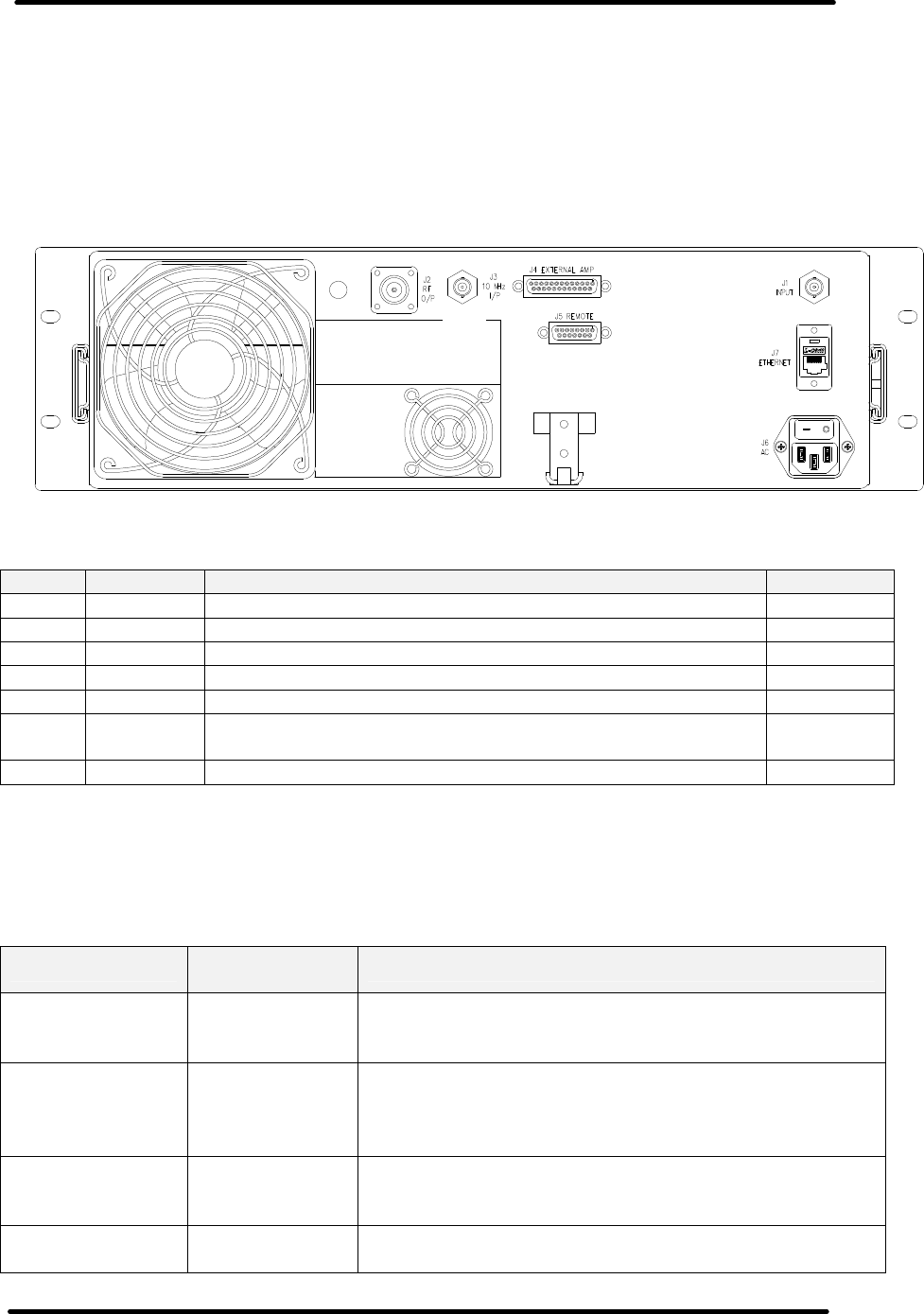
30W Driver Tray Input and Output Connections
The input connections to the 30W Driver Tray are made to the jacks mounted on the rear
of the tray. The tray accepts an On Channel RF signal at J1, the RF input jack, and
outputs a digital RF ON Channel signal at J2, the RF Output Jack. A 10 MHz reference
input connects to J3 on the tray. Refer to Figure 2 and to Table 4 that follow for detailed
information.
Figure 2: Rear View of the 30W Driver Tray.
Table 4: Rear Chassis Connections for the Driver Tray.
Port Type Function Impedance
J1 BNC RF Input: On Channel RF Input 75O
J2 N RF Output: On Channel RF Output 50O
J3 BNC 10 MHz Input: External 10 MHz Reference Input 50O
J4 25 Pos D External Amplifier: Interface to external amplifier tray N/A
J5 16 Pos D Remote: Remote control and status indications N/A
J6 IEC AC Input: AC input connection and On/Off circuit
breaker N/A
J7 Ethernet: (Optional Ethernet connection) N/A
Remote Connections
The remote connections for the Driver Tray are made to the Remote 15 Pos “D” connector
Jack J5 located on the rear panel of the tray.
Table 5: Remote Connections to J5 for the Driver Tray.
Signal Name J5 Pin
Designations Signal Type/Description
RMT
Transmitter
Operate 1 Discrete Open Collector Input - A pull down to
ground on this line indicates that the transmitter is
to be placed into the operate mode.
RMT
Forward Power 2
Analog Output - 0 to 4.0 V- This is a buffered loop
through of the calibrated “System Forward Power ”.
Indicates the transmitter's Forward power. Scale
factor is 100 % / 3.2V.
RMT
Transmitter
Standby 3 Discrete Open Collector Input - A pull down to
ground on this line indicates that the transmitter is
to be placed into the standby mode.
Ground 4,8,9,10 & 14 Ground pins available for remote
J4
J5
J1
J7
J6
J3
J2
J3

Innovator CU250ATD, 250 Watt Transmitter Tray Description
Instruction Manual, Rev. 0 15
Signal Name J5 Pin
Designations Signal Type/Description
RMT RF System
Interlock 5 When this signal's circuit is completed to ground, the
transmitter is allowed to operate. If this circuit is
opened, the transmitter switches to Standby.
RMT
Reflected Power 6
Analog Output - 0 to 4.0 V- This is a buffered loop
through of the calibrated “System Reflected Power ”.
Indicates the transmitter's Reflected power. Scale
factor is 100 % / 3.2V.
RMT
Fault Reset 7 Discrete Open Collector Input - A pull down to
ground on this line indicates that any transmitter
Faults are to be reset.
RMT
Operate Status 11 Discrete Open Collector Output - A low indicates that
the Transmitter is in Operate.
RMT
Fault 13 Discrete Open Collector Output - A low indicates that
the Transmitter has a Fault.
RMT
Input Fault 15 Discrete Open Collector Output - A low indicates that
the Transmitter has an Input Fault.
Not Used 16 N/A

Innovator CU250ATD, 250 Watt Transmitter Front Panel Screens Description
Instruction Manual, Rev. 0 16
Front Panel Screens for the Transmitter
A LCD display located on the front of the Driver Tray displays the current operating
status of the transmitter. The screens are scrolled through using the buttons to the right
of the display. The Left & Right Arrows scroll through the Main Menus, which are shown
below aligned on the left side. The Up & Down Arrows scroll through the Submenus of the
Main Menus, when they are present, which are shown below indented under the Main
Menu in which they are contained. The ENTER button selects the changes made. The
following screens are typical of an operating transmitter.
Table 6: Transmitter Forward Power Screen
This screen provides an indication of the Output Power of the transmitter in terms of
Percent. There are no adjustments on this menu.
Table 7: Transmitter Reflected Power Screen
This screen provides an indication of the Reflected Power of the transmitter in terms of
Percent. There are no adjustments on this menu
Table 8: Heatsink Temperature Screen
This screen shows the temperature of the amplifier heatsink assembly, mounted in the
transmitter, in degrees F. If the temperature is below the trip point, it will indicate OK.
Table 9: Demodulator Status Screen
This menu indicates whether there is a signal present at the demodulator. This menu
only provides status information and no adjustments are available.
This menu indicates whether the Phase Lock Loop is locked in the demodulator.
This menu only provides status information and no adjustments are available.
This screen provides the user information on the signal to noise ratio and the
signal level of the receive signal. The signal strength allows the user to optimize
the position of the receive antenna. The signal strength ranges from 0 to 100 %
and typically should be above 40 % for reliable operation. Signal to noise ratio is
also provided on this menu to indicate to the user the quality of the receive
signal. This reading may also assist the user in the positioning of the antenna.

Innovator CU250ATD, 250 Watt Transmitter Front Panel Screens Description
Instruction Manual, Rev. 0 17
Table 10: Modulator Status Screen
This menu indicates if the modulator has an SMPTE-310 signal input coming from the
demodulator. This menu only provides status information and no adjustments are
available.
This menu indicates if the Phase Lock Loop A in the modulator is locked. This
menu only provides status information and no adjustments are available.
This menu indicates if the Phase Lock Loop B in the modulator is locked. This
menu only provides status information and no adjustments are available.
Table 11: IF Processor Screen
This menu indicates whether there is a signal present to the IF processor from the
modulator. This menu only provides status information and no adjustments are
available.
This menu indicates if the IF Signal to the IF Processor has modulation. This
menu only provides status information and no adjustments are available.
Table 12: AGC Status Screen
This menu indicates if the AGC circuit has an input. This menu only provides status
information and no adjustments are available.
This menu indicates if the AGC circuit is operating within its range. This menu
only provides status information and no adjustments are available.
This menu indicates if the AGC circuit is operating in Auto or Manual. This menu
only provides status information and no adjustments are available.
This menu indicates the Auto ALC voltage setting. This menu only provides
status information and no adjustments are available.
Innovator CU250ATD, 250 Watt Transmitter Front Panel Screens Description
Instruction Manual, Rev. 0 18
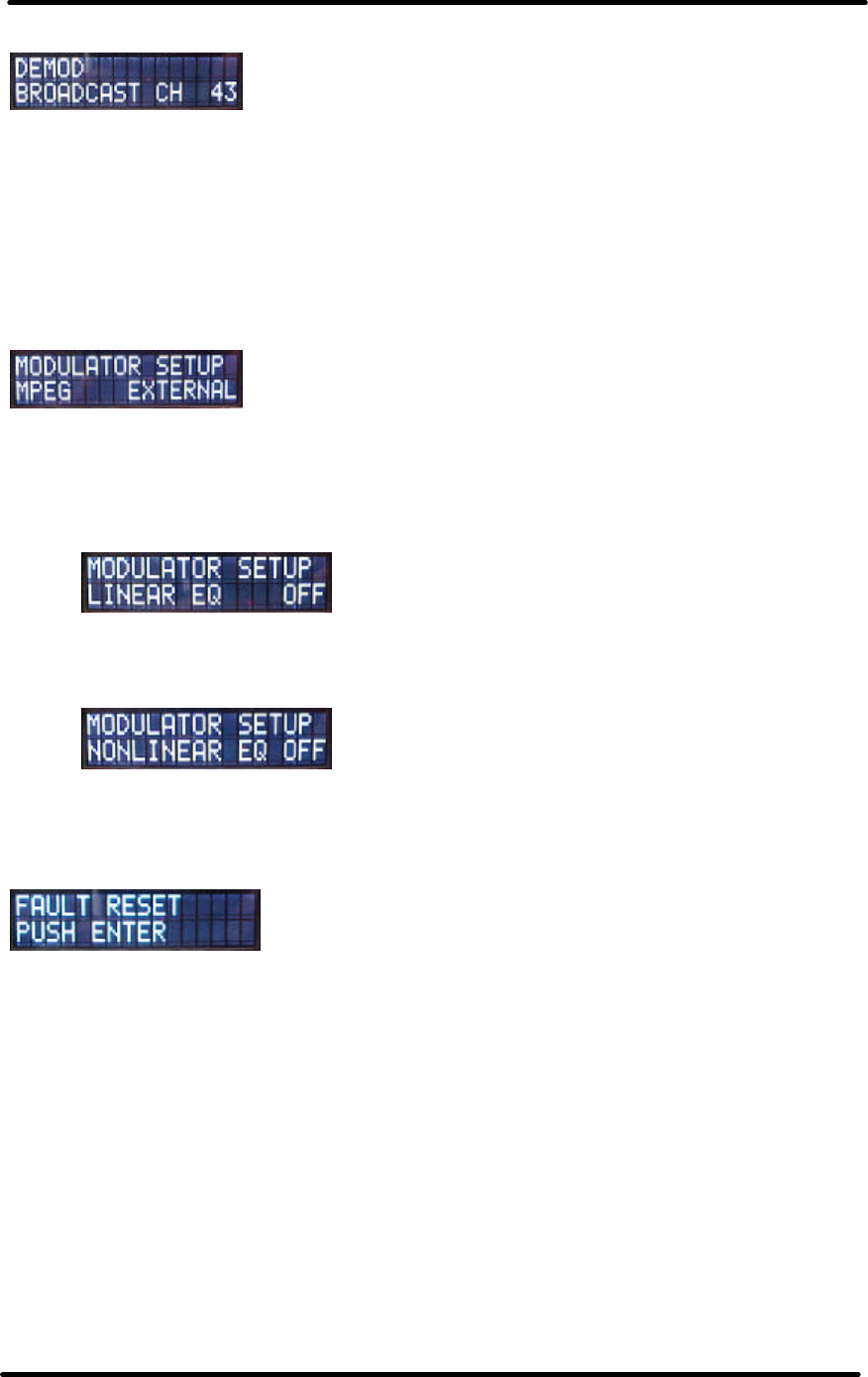
Table 13: Demodulator Channel Set Up Screen
The channel setup screen can be accessed by holding the left and right arrow keys down
until the setup screen is displayed. Once the user is in this menu, the channel plan can
be changed to either broadcast or cable by hitting the ENTER button. In addition, the
receive channel can be changed by hitting the up or down arrow to select the channel.
After the selections have been made, the user needs to depress the right or left arrow
again and then the display will ask “PUSH ENTER TO ACCEPT CHANGES”. If the ENTER
button is depressed, the changes will be accepted. If any other key is chosen, the
changes will not be made.
Table 14: Modulator Set Up Screen
This screen allows the user to select between an internal or external source in the
modulator. During the installation of the system, an off air signal may not be available
to the modulator, therefore the user can set the source to INTERNAL to generate an 8
VSB signal from the unit that can be used for set up. Once a receive signal is available,
the source should be set to EXTERNAL
This screen controls the operation of the linear equalizer. When set to ON, the
modulator applies linear correction to the IF output. When set to OFF, no
correction is applied to the IF.
This screen controls the operation of the nonlinear correction. When set to ON,
the modulator applies nonlinear correction to the IF output. When set to OFF, no
correction is applied to the IF.
Table 15: Fault Reset Menu
This screen allows the user to reset any previous faults that may have occurred in the
tray. When a fault is present in the tray, the status LED on the front panel will flash
RED as long as the fault is present. In addition, the menu will jump to the present fault
on the display and blink this fault continuously. When the fault goes away, the tray will
turn the status LED to AMBER to indicate that there was a fault and the menu will still
display the fault but it will not flash. This allows the user to know that there was a fault
and what type of fault occurred. To reset the indication of a previous fault, the user can
hit the ENTER button when this screen is visible and all of the faults will be cleared.
This completes the description of the menu screens for the transmitter.

Innovator CU250ATD, 250 Watt Transmitter System Alignment
Instruction Manual, Rev. 0 19
CU250ATD Innovator 250-Watt Transmitter
Figure 3: Front View of the 250W Power Amplifier Tray.
250W Power Amplifier Tray Description
The 250-Watt Power Amplifier Tray accepts an RF On Channel signal from the 30-Watt
driver tray and amplifies the signal to a power level of 250 Watts.
2-Way Splitter Board (1308933)
The 2-Way Splitter Board splits the incoming RF signal from the 30W Driver Tray and
applies the two RF signal paths to (2) 600W PEP UHF Amplifier Pallets.
600W PEP RF Pallet (LDU601-C) x2
The 600W PEP RF Pallet amplifies an incoming UHF RF signal and provides +18 dB gain.
The pallet is powered by a +30VDC source. Two pallets are required.
2-Way Combiner Board (1308930)
The 2-Way Combiner Board combines the two RF output signals from each 600W PEP RF
Pallet.
Amplifier Control Board (1308936)
The Amplifier Control Board receives commands from the 30W Driver Tray to control the
250W Amplifier Tray. The board also monitors the status, faults and power levels of the
amplifier tray and sends these signals back to the 30W Driver tray to be monitored on
the Driver’s LCD display.
+12VDC Switching Power Supply (1308896)
The +12VDC Switching Power Supply Board supplies +12VDC to power the Amplifier
Control Board.
+30VDC Switching Power Supply (1308906)
The +30VDC Switching Power Supply supplies +30VDC to power both 600W PEP RF
Pallets.
Innovator CU250ATD, 250 Watt Transmitter System Alignment
Instruction Manual, Rev. 0 20
Table 6: 250W UHF Amplifier Tray Operate/Standby Indicators
LED FUNCTION
ENABLE
(Green) When lit, indicates that the system is in Operate. When
extinguished, indicates that the system is in Standby.
STATUS
(Green/Red/
Amber)
A Green LED indicates that the system is functioning normally. A
flashing Red LED indicates a fault is occurring at this time. An
Amber LED indicates a fault occurred in the past but the system
is now operating normally.
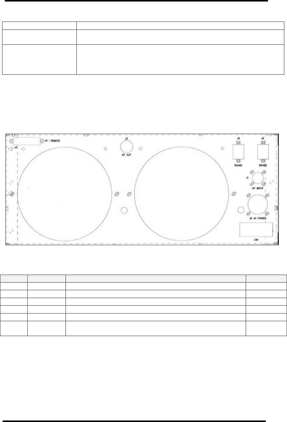
250W Power Amplifier Tray Input and Output Connections
The input connections to the amplifier tray are made to the jacks mounted on the rear of
the amplifier tray. The tray accepts an On Channel RF signal at J1, the RF input jack,
and outputs a digital RF ON Channel signal at J2, the RF Output Jack. Refer to Figure 3
and to Table 7 that follow for detailed information.
Figure 3: Rear View of the 250W Power Amplifier Tray.
Table 7: Rear Chassis Connections for the Power Amplifier Tray.
Port Type Function Impedance
J1 N RF Input: On Channel RF Input 50O
J2 N RF Output: On Channel RF Output 50O
J3 Ethernet: (Optional Ethernet connection) N/A
J4 25 Pos D Remote: Interface to Driver tray N/A
J5 Ethernet: (Optional Ethernet connection) N/A
J6 Circular AC Input: AC input connection and On/Off circuit
breaker N/A

Innovator CU250ATD, 250 Watt Transmitter System Alignment
Instruction Manual, Rev. 0 21
System Alignment
This transmitter was aligned at the factory and should not require additional
adjustments to achieve normal operation.
This transmitter is of a tray design with multiple boards inside the tray. If a board fails,
that board needs to be changed out with a replacement board. The failed board can then
be sent back to Axcera for repair. Contact Axcera Customer Service Department at 724-
873-8100 or fax to 724-873-8105, before sending in any board or module.
Set Up of the Output Power of the Transmitter
Check that the Auto/Man switch S1 on the IF Pre-Corrector Board is in the Automatic ALC
position. This is the normal operating position for the switch. The voltage at TP1 on the
IF Pre-Corrector Board should be .8 VDC with 100% output power.
Check that the Auto/Man switch S1 on the ALC Board is in the Automatic ALC position.
Adjust R75 the ALC pot on the ALC Board as needed to attain 100% output power. Switch
to Manual Gain (Manual ALC) and adjust the Manual Gain pot R62 for 100 % output
power. Switch the ALC Board back to Automatic ALC.
ALC Board Set-Up In the Tray
On (A5) the ALC Board (1308570), preset the Overdrive Threshold pot R38 full CW and
set R62, Manual Adjust, and R75, ALC Adjust, full CCW.
Apply an 8-VSB signal at -3 dBm average level to the J1 input jack to the tray. Switch
S1 to Manual Gain, and increase the output power to 100%. Calibrate the transmitter
output power using R23, Forward Calibration pot, on the Output Detector Board.
Turn the output power down to 10% power. Remove the output RF connector from J2
on tray and calibrate the reflected power to 10%, using R7, the Reflected Calibration
pot, on the Output Detector Board. Re-connect the RF output connector to the tray and
increase the power, in Manual gain, to 110%. Adjust the Overdrive pot R38, CCW until
the overdrive threshold just trips and the Overdrive Fault LED DS4 lights. Turn the pot
slightly CW so that power comes back up and DS4 goes out.
Switch S1 to ALC. Turn the ALC Adjust pot R75 until the power is 100%. Switch S1
between ALC and Manual to verify smooth switching, with minimal change in power.
Switch the tray Off and insert a 10 dB attenuator at the input. Switch the tray On and
verify the input fault LED comes on and the RF power Mutes. Output power should drop
by at least 20-30 dB.
Switch the tray Off and remove the 10 dB attenuator. Replace the input connector and
turn the tray back on. With the tray in ALC, use the ALC Adjust pot, R75, to decrease
the power to 10%. Remove the RF output connector from the tray. Verify that the
VSWR Cutback LED, DS6, comes on and the Reflected Power drops to approximately
6%. Reconnect the RF output connector and increase the power back up to 100%.
This completes the set up of the ALC board.

Innovator CU250ATD, 250 Watt Transmitter System Alignment
Instruction Manual, Rev. 0 22
6 MHz
-35 dB
-110 dB
3 MHz 6 MHz
Figure 3: Typical Digital Spectrum
Linearity Correction Adjustment (Non-Linear Distortions)
As shipped, the transmitter was preset to include amplitude and phase pre-distortion. The
pre-distortion was adjusted to approximately compensate the corresponding non-linear
distortions of the Power Amplifier.
NOTE: On (A3) the IF pre-corrector board (1308796), check that the correction
enable/disable jumper W4 on J8 is in the Enable position, between pins 2 & 3.
Set up a spectrum analyzer with 30 kHz resolution bandwidth and 30 kHz video
bandwidth to monitor the intermodulation products of the RF output signal of the Tray at
J2. A typical digital spectrum is shown in Figure 3.
There are three Corrector stages, two in phase and one quadrature, adjustments located
on the IF Pre-Corrector Board. The adjustments are threshold settings that are adjusted
as needed to correct for any amplitude or phase intermod problems. Adjust in phase
linearity correction adjustment R67 threshold 1 cut in for the in phase amplitude
distortion pre-correction that is needed. Next adjust the linearity correction adjustment
R69 threshold 2 cut in also for the in phase amplitude distortion pre-correction that is
needed. Finally, adjust the quadrature linearity correction adjustment R89, threshold
cut in, for the quadrature phase distortion pre-correction that is needed. The above pots
are adjusted for the greatest separation between the digital signal and the intermod at
the channel edges.
Frequency Response Delay Equalization Adjustment at 44 MHz
The procedure for performing a frequency response delay equalization adjustment for the
transmitter is described in the following steps. Check that the jumpers on J4, J5 & J6 are
set for 44 MHz between Pins 2 & 3.
The center frequency for the first stage is 46.5 MHz. Adjust R24, located on the IF Pre-
Corrector Board, for the best depth of frequency response correction at 46.5 MHz. C14
may need to be adjusted to attain best depth at 46.5 MHz.

Innovator CU250ATD, 250 Watt Transmitter System Alignment
Instruction Manual, Rev. 0 23
The center frequency for the second stage is 41.5 MHz. Adjust R25 for the best depth of
frequency response correction at 41.5 MHz. C15 may need to be adjusted to attain best
depth at 41.5 MHz.
The center frequency for the third stage is 44 MHz. Adjust R26 for the best depth of
frequency response correction at 44 MHz. C16 may need to be adjusted to attain best
depth at 44 MHz.
After the three delay attenuation equalizers have been adjusted, fine tune, as needed, for
the best frequency response across the channel.
The transmitter is now set up and ready for normal operation.
If a problem occurred during the set up, help can be found by calling Axcera field support
at 724-873-8100.
APPENDIX A
DRAWINGS LIST

Innovator CU250ATD, Appendix A,
250 Watt Transmitter Drawings List
CU250ATD Transmitter, Rev. 0 A-1
CU250ATD Innovator Transmitter
30-Watt Driver Tray
30-Watt Driver Tray Block Diagram..................................................................1308815
8 VSB Modulator Board Schematic...................................................................1308276
Power Conditioning Board Schematic................................................................1309405
Digital Modulator Board Schematic...................................................................1304884
Pre-Corrector Board Schematic........................................................................1308797
ALC Board Schematic .....................................................................................1308571
Output Detector Board Schematic....................................................................1308686
Control Card Board Schematic.........................................................................1308817
Frequency Agile Upconverter Board Schematic .................................................1309696
Two Stage UHF Amplifier Board Schematic........................................................1308785
Amplifier Module Schematic ......................................................... 51-5379-308-00-WSP
Astec Switching Power Supply Documentation.......................................................LPT62
Densei-Lamda Switching Power Supply Documentation...................................... SWS600
250-Watt Power Amplifier Tray
250-Watt Power Amplifier Block Diagram..........................................................1308400
250-Watt Power Amplifier Interconnect ............................................................1309077
2-Way Splitter Board......................................................................................1308934
600W PEP RF Pallet ......................................................................................LDU-601C
2-Way Combiner ..........................................................................................1308931
Amplifier Control Board...................................................................................1308937
V-Infinity Switching Power Supply Documentation.............................................1308896
Power Magnetics Switching Power Supply .........................................................1308906
APPENDIX B
TRANSMITTER SPECIFICATIONS
DIGITAL
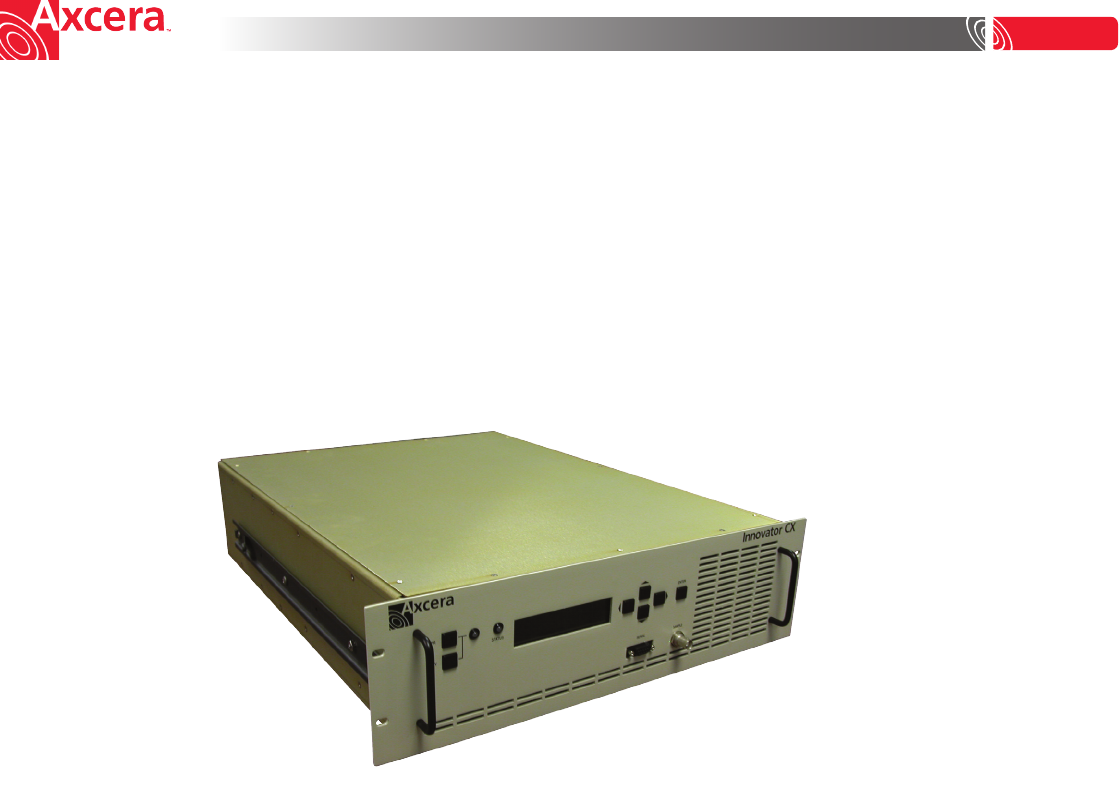
INNOVATOR CX
Low Power UHF DTV Transmitter/Translator 5W - 250W
Designed to provide broadcasters a cost effective product that will meet their
needs like no other solution on the market, this new low power transmitter
line uses the latest LDMOS devices for broadband operation across the entire
UHF band, and can be configured as a DTV transmitter or regenerative
translator. This allows users to minimize spare parts stock, which is especially
important to multi-transmitter operators, and also enables simple and
inexpensive channel changes
Each very compact unit is completely contained within a single 3RU rackmount
tray up to 50 watts, including the digital receiver and modulator. Monitoring is
simple with the optional secure Web browser/SNMP interface, allowing users to
access all transmitter operating and control parameters through any computer
with Internet access.

DIGITAL
INNOVATOR CX
Low Power UHF DTV Transmitter/Translator 5W - 250W
Specifications published here are current as of the date of publication of this document. Because we are continuously improving our products, Axcera reserves the right to change specifications without prior notice.
At any time, you may verify product specifications by contacting our office. Axcera views it’s patent portfolio as an important corporate asset and vigorously enforces its patents. Products or features contained
herein may be covered by one or more U.S. or foreign patents.
0711R0 © 2007 AXCERA All Rights Reserved An Equal Opportunity Employer
103 Freedom Drive, PO Box 525, Lawrence, PA 15055, USA t:+1 724-873-8100 f:+1 724-873-8105 www.axcera.com Innovator CX UHF DTV Tx
Options
AC Surge Protector
GPS Receiver
Stringent Mask Filter
Spare Parts Kit
Climate Controlled Outdoor Enclosure
Equipment Rack
1 Consult factory for other frequencies, voltages or altitudes
2 Measured in 30KHz RBW, relative to total average power
Model Information
Model Numbers CU5ATD CU30ATD CU50ATD CU125ATD CU250ATD
CU5ARD CU30ARD CU50ARD CU125ARD CU250ARD
Power Output 5W 30W 50W 125W 250W
Power Consumption 180W 400W 500W 1100W 1700W
Input Power1
Line Voltage (VAC) 100-240 208-240 ±10%
Power Requirements Single Phase, 50 or 60 Hz
Size (19” rackmount) 3RU 7RU
Weight (lbs) 40 45 50 150 150
Maximum Altitude1 8500ft (2600m) AMSL
Operational Temperature Range 0 to +50º, derate 2ºC/1000 ft
Operational Humidity Range 0% to 95% non-condensing
Specifications
General Output Parameters
Standard ATSC
Connector Type N
Impedance 50 Ohms
Bandwidth 6 MHz
Test Signal Internal PRBS-23
Frequency Range1 470 to 806 MHz
Frequency Stability ±1 ppm (max. 30 day variation)
w/precise frequency control ±2Hz
Regulation of Output Power 3%
Out of Band2 Compliant with FCC Simple
or Stringent DTV Mask
SNR 32 dB (typical), 30dB (min.)
Input Parameters (Transmitter)
Connector Type BNC
Data Interface
Input Rate 19.39Mbps, 6MHz Channel
Input Interface SMPTE 310M (ASI optional)
Input Parameters (Translator)
Frequency Range 54 to 806 MHz
Connector Type BNC
Impedance 50 Ohms
Level -78 to -8 dBm
White Noise Threshold of Errors Better than 15.5 dB
Equalization Range Better than ±45 μsec