UBS Axcera DT325B 350-Watt VHF Low Band Digital Transmitter User Manual title page DT325B
UBS-Axcera 350-Watt VHF Low Band Digital Transmitter title page DT325B
Contents
- 1. Axciter Modulator User Manual Part 1
- 2. Axciter Modulator User Manual Part 2
- 3. Compiled Exciter Users Manual
Compiled Exciter Users Manual
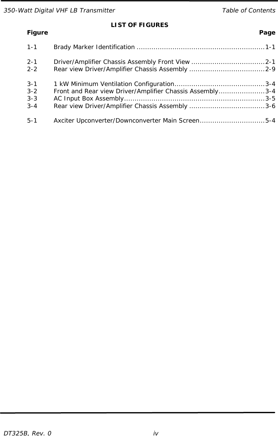
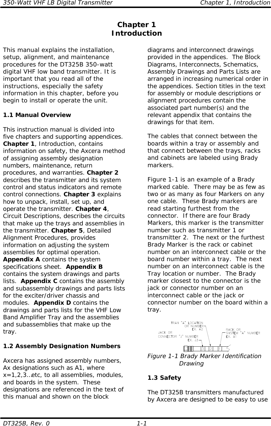
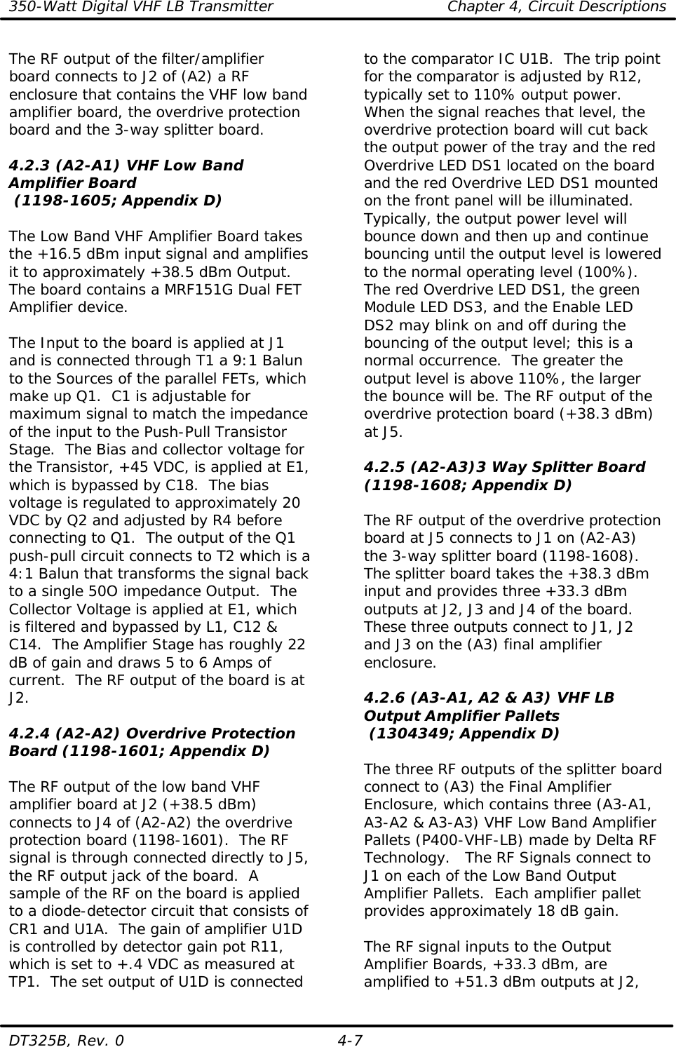
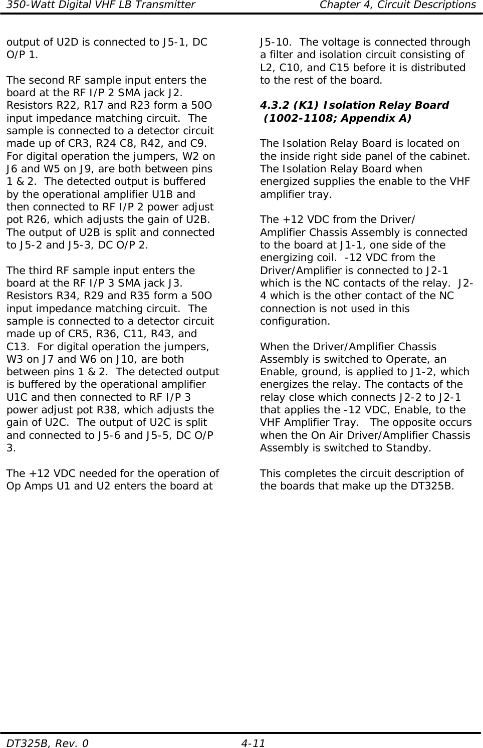
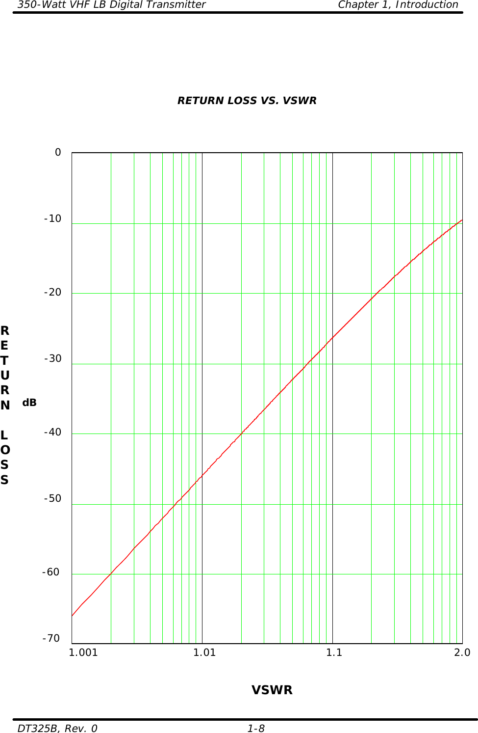
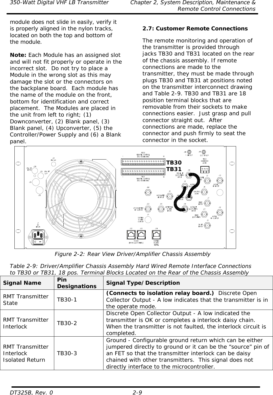
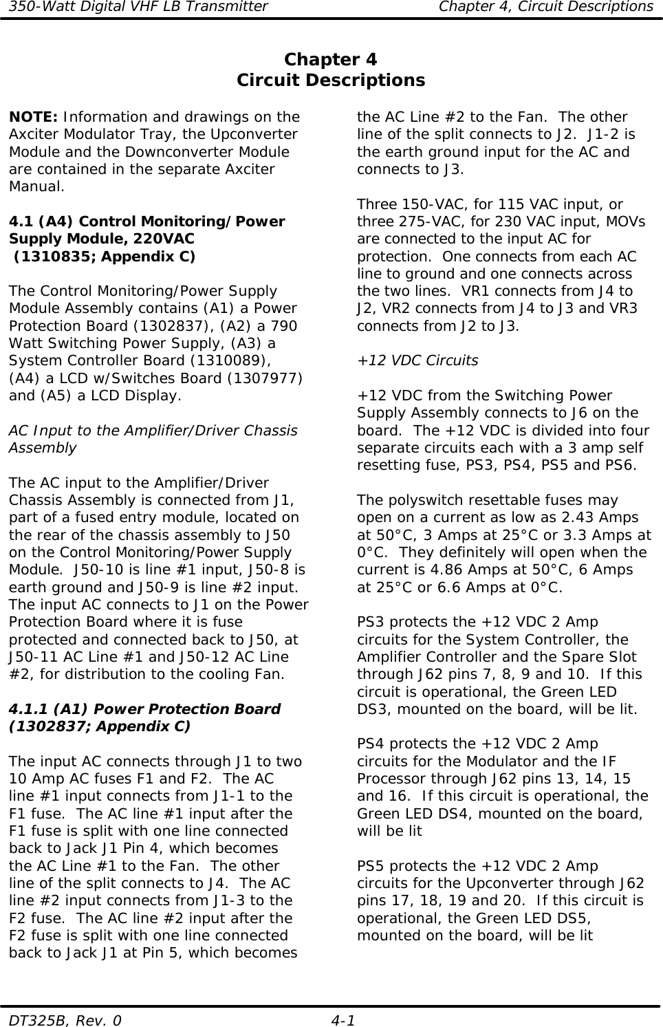
![350-Watt VHF LB Digital Transmitter Chapter 1, Introduction DT325B, Rev. 0 1-6 dBm, dBw, dBmV, dBµV, & VOLTAGE EXPRESSED IN WATTS 50 Ohm System WATTS PREFIX dBm dBw dBmV dBµV VOLTAGE 1,000,000,000,000 1 TERAWATT +150 +120 100,000,000,000 100 GIGAWATTS +140 +110 10,000,000,000 10 GIGAWATTS +130 +100 1,000,000,000 1 GIGAWATT +120 + 99 100,000,000 100 MEGAWATTS +110 + 80 10,000,000 10 MEGAWATTS +100 + 70 1,000,000 1 MEGAWATT + 90 + 60 100,000 100 KILOWATTS + 80 + 50 10,000 10 KILOWATTS + 70 + 40 1,000 1 KILOWATT + 60 + 30 100 1 HECTROWATT + 50 + 20 50 + 47 + 17 20 + 43 + 13 10 1 DECAWATT + 40 + 10 1 1 WATT + 30 0 + 77 +137 7.07V 0.1 1 DECIWATT + 20 - 10 + 67 +127 2.24V 0.01 1 CENTIWATT + 10 - 20 + 57 +117 0.707V 0.001 1 MILLIWATT 0 - 30 + 47 +107 224mV 0.0001 100 MICROWATTS - 10 - 40 0.00001 10 MICROWATTS - 20 - 50 0.000001 1 MICROWATT - 30 - 60 0.0000001 100 NANOWATTS - 40 - 70 0.00000001 10 NANOWATTS - 50 - 80 0.000000001 1 NANOWATT - 60 - 90 0.0000000001 100 PICOWATTS - 70 -100 0.00000000001 10 PICOWATTS - 80 -110 0.000000000001 1 PICOWATT - 90 -120 TEMPERATURE CONVERSION °F = 32 + [(9/5) °C] °C = [(5/9) (°F - 32)]](https://usermanual.wiki/UBS-Axcera/DT325B.Compiled-Exciter-Users-Manual/User-Guide-1001239-Page-11.png)
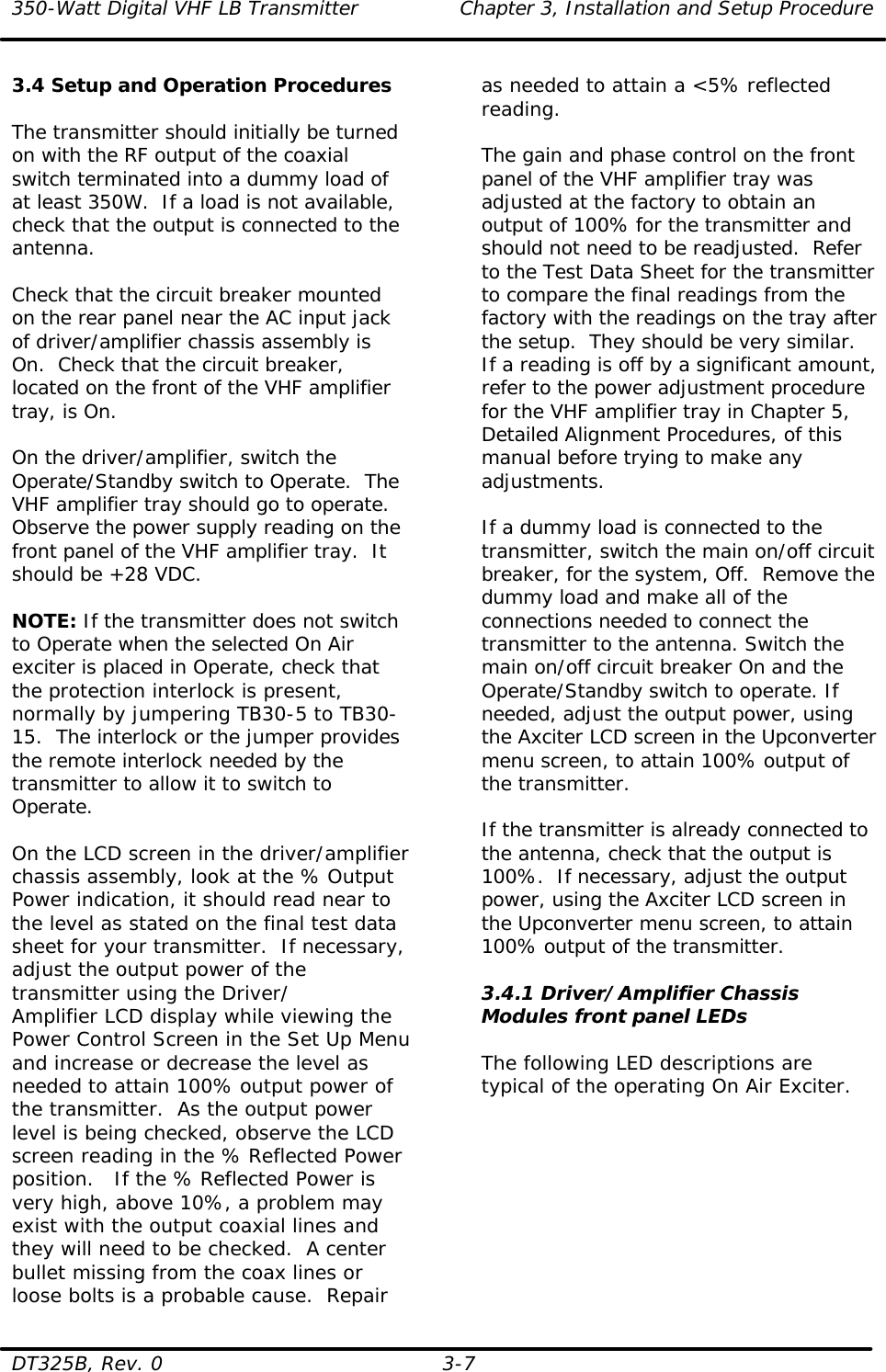
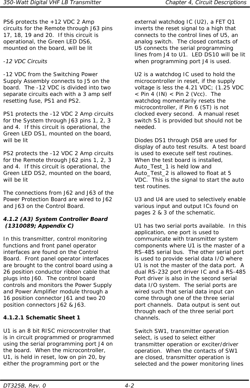
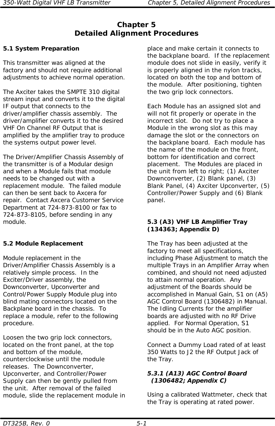
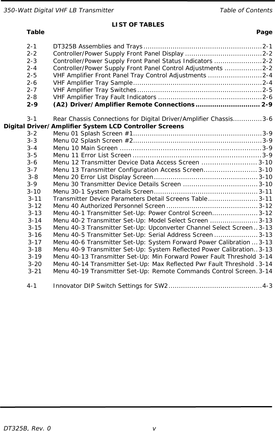
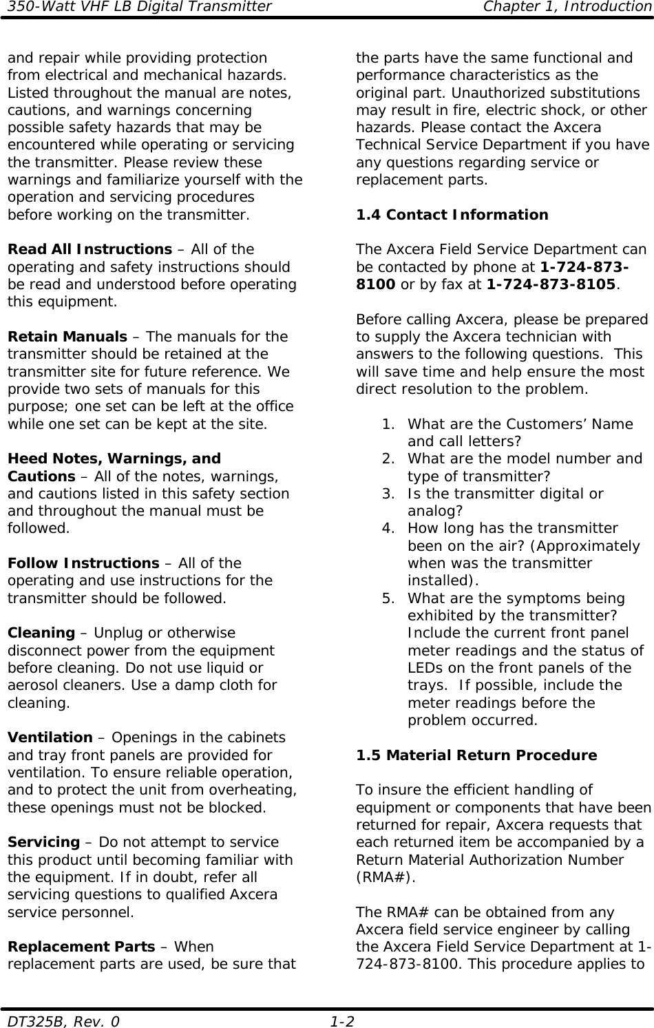
![350-Watt Digital VHF LB Transmitter Chapter 4, Circuit Descriptions DT325B, Rev. 0 4-5 that supplies the information from the selected source to the display. By pushing the button again, a different source is selected. This occurs for each push button. Refer to Chapter 3 for more information on the Display Menu Screens. 4.1.4 (A2) Switching Power Supply Assembly The power supply module contains a switching power supply, a terminal blocks, V1, V2 & V3, for distributing the DC voltages, and a 3 position terminal block to which the AC Input connects. Jack J1 connects to the Control Board and supplies DC OK, at J1-4 & 3, and AC OK, at J1-2 & 1, status to the control board. A Power Supply enable connects from the control board to the power supply at V1B-6 & 7. The power supply is configured for three output voltages +12V, -12V, at the 10 position terminal block, and a main output power of +32 VDC at J50 pin A (+) and J50 pin B (Rtn). The power supply is power factor corrected to .98 for optimum efficiency and decrease in energy consumption. For safety purposes all outputs are over voltage and over current protected. This supply accepts input voltages from 85 to 264 volts AC, but the power entry module, for the exciter/amplifier chassis, must be switched to the proper input voltage setting, for the transmitter to operate. 4.1.5 RF Output of Driver/Amplifier Chassis Assembly The RF output from the upconverter at the upconverter RF output jack J23, a BNC connector. The RF is cabled to the “S” input Jack on the (A10) 2 Way Splitter. One output of the splitter connects to the VHF Amplifier Tray. The other output of the splitter connects to the triple peak detector board for metering, ALC and monitoring purposes. NOTE: Information and drawings on the Axciter Modulator Tray, the Upconverter Module and the Downconverter Module are contained in the separate Axciter Manual. This completes the description for the Driver/Amplifier chassis assembly. 4.2 (A3) VHF Low Band Amplifier Tray (1304363; Appendix D) The VHF low band amplifier tray is adjusted at the factory for use as a digital RF amplifier tray. The tray has approximately 55 dB of gain at the frequency of the VHF low band channel and will take the typical +4 dBm DTV input and amplify it to an output level of approximately +55.8 dBm. As a DTV amplifier, the tray is calibrated for 350 watts average power that is equal to a 100% meter reading. The tray is made up of the boards and assemblies listed in Table 4-1. Table 4-1: VHF Low Band Amplifier Tray Boards and Assemblies MAJOR ASSEMBLY DESIGNATOR BOARD/ASSEMBLY NAME DRAWING NUMBER A1-A1 Phase shifter board (mounted in [A1] an RF enclosure assembly) 1198-1602 A1-A2 Filter/amplifier board (mounted in [A1] an RF enclosure assembly) 1198-1606 A2-A1 VHF low band amplifier board (mounted in [A2] an RF enclosure assembly) 1198-1605 A2-A2 Overdrive protection board (mounted in [A2] an RF enclosure assembly) 1198-1601](https://usermanual.wiki/UBS-Axcera/DT325B.Compiled-Exciter-Users-Manual/User-Guide-1001239-Page-44.png)
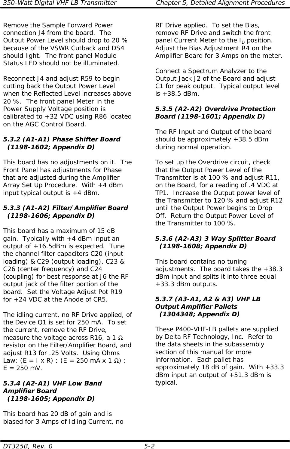
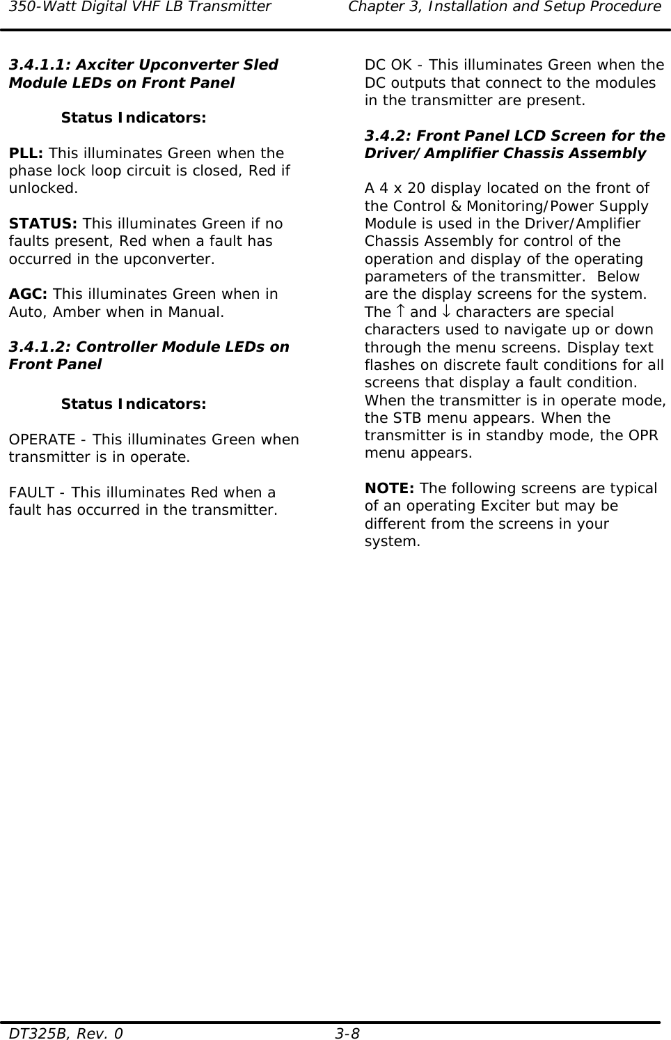
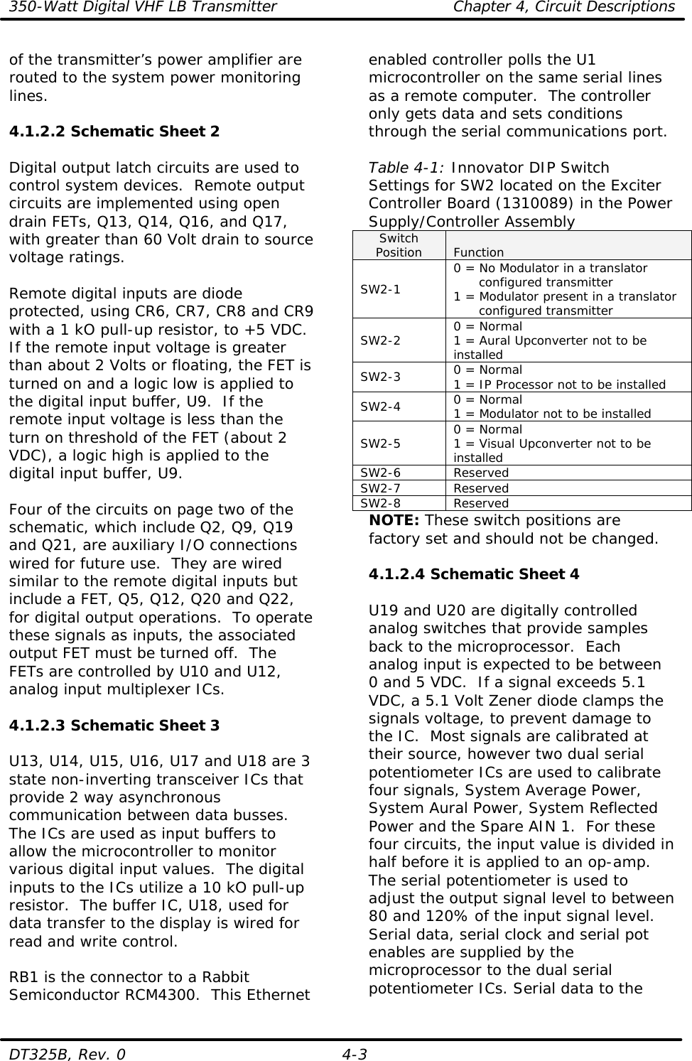
![350-Watt Digital VHF LB Transmitter Chapter 4, Circuit Descriptions DT325B, Rev. 0 4-6 A2-A3 3-way splitter board (mounted in [A2] an RF enclosure assembly) 1198-1608 A3-A1, A3-A2 and A3-A3 Three low band VHF amplifier pallets (mounted in [A3] an RF enclosure assembly) P400-VHF-L-18 1304348 A4-A1 3-way combiner board (mounted on [A4] the 3 way combiner enclosure) 1198-1626 A4-A2 & A4-A3 Low pass filter board (mounted on [A4] the 3 way combiner enclosure) 1198-1628 A5 AGC control board 1306482 A8 Current metering board 1304362 A10 +30 VDC switching power supply assembly PM3329B-5-1-R-2-E 1301504 4.2.1 (A1-A1) Phase Shifter Board (1198-1602; Appendix D) The On Channel RF signal (+4dBm), enters the rear of the Tray at the "BNC" Jack J1 and is fed to J1 of the (A1) Enclosure Assembly which contains the phase shifter board and the filter amplifier board. The input is cabled to to J1 of (A1-A1) the Phase Shifter Board (1198-1602). The Board provides a Phase Shift adjustment of the RF Signal that is needed to provide maximum output during the combining of multiple Amplifier Trays in an Amplifier Array. A front panel mounted Phase Shift Potentiometer, R2 (A7), which connects to J3 of the Board, controls the Phase of the RF Signal. If the Input Signal level to the Phase Shifter Board falls below a preset level, a High, which is an Input Fault, connects from J5 of the board to J14 on the AGC Control Board. When an Input Fault occurs, the AGC Control Board generates a Fault Output at J1, which is connected to J4 on the Filter/Amplifier Board. The Fault cuts back the RF Signal level using the Pin Diode Attenuator Circuit located on the Filter/Amplifier Board. The output at J2 of the Phase Shifter Board is directed to J7 the input jack on (A1-A2) on the filter/amplifier board. 4.2.2 (A1-A2) Filter/Amplifier Board (1198-1606; Appendix D) The phase-controlled output (+4 dBm) at J2 of the phase shifter board is directed to J7, the input jack of the (A1—A2) filter amplifier board (1198-1606) that is made up of two circuits. The first circuit is a channel filter that is adjusted for the desired channel frequency and bandwidth. The filtered output (+2 dBm) is connected to the second circuit that contains two amplifiers. The RF connects through a pin-diode circuit to the amplifier IC U1. The voltage applied to J4, which is the external control jack of the board, controls the amplitude of the RF signal through the pin-diode attenuator circuit. Jumper W1 on J5 should be between pins 2 and 3, which provide external control, through J4, of the gain of the board, as well as the output level of the tray. R9 is the manual gain pot that is in the circuit when the jumper W1 is between pins 1 & 2. The front panel mounted gain pot R3 (A6) connects to the AGC control board and is used to adjust the AGC pin-attenuator bias voltage that connects to J4 on the filter/amplifier board. The RF signal, after the pin-attenuator circuit, is amplified by the second amplifier stage Q1 to about +16.5 dBm; this signal is connected to the output of the board at J2.](https://usermanual.wiki/UBS-Axcera/DT325B.Compiled-Exciter-Users-Manual/User-Guide-1001239-Page-45.png)