UBS Axcera HU5000BTD 5000-Watt UHF Digital Transmitter User Manual Title Page Vol 2
UBS-Axcera 5000-Watt UHF Digital Transmitter Title Page Vol 2
UserManual.wiki
>
UBS Axcera
>
HU5000BTD User Manual
>
User manual 4
Contents
1.
User manual 1
2.
User manual 2
3.
User manual 3
4.
User manual 4
User manual 4
Navigation menu
Upload a User Manual
Namespaces
Wiki Guide
HTML
PDF
Info
Views
User Manual
Discussion / Help
Navigation


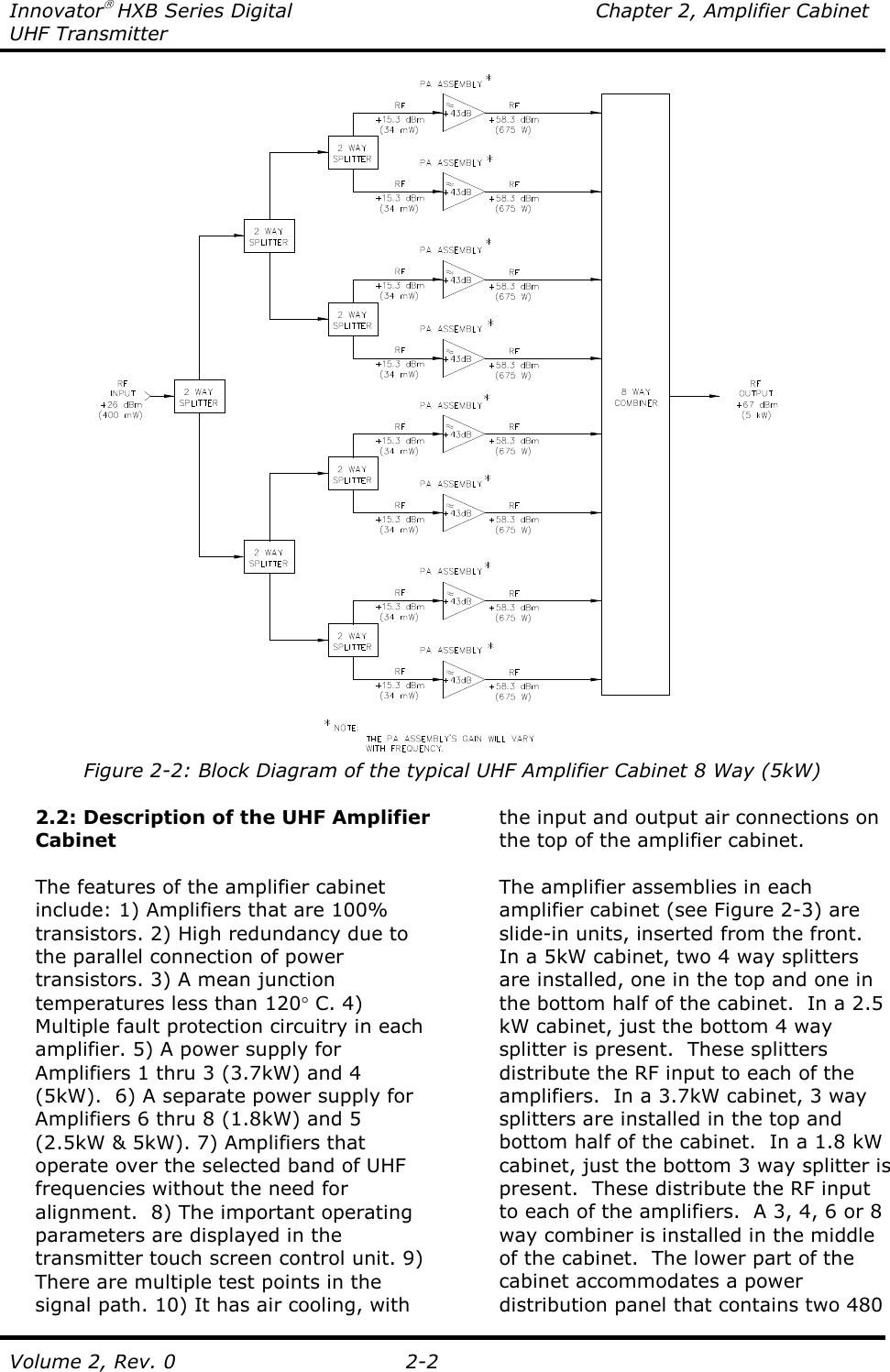
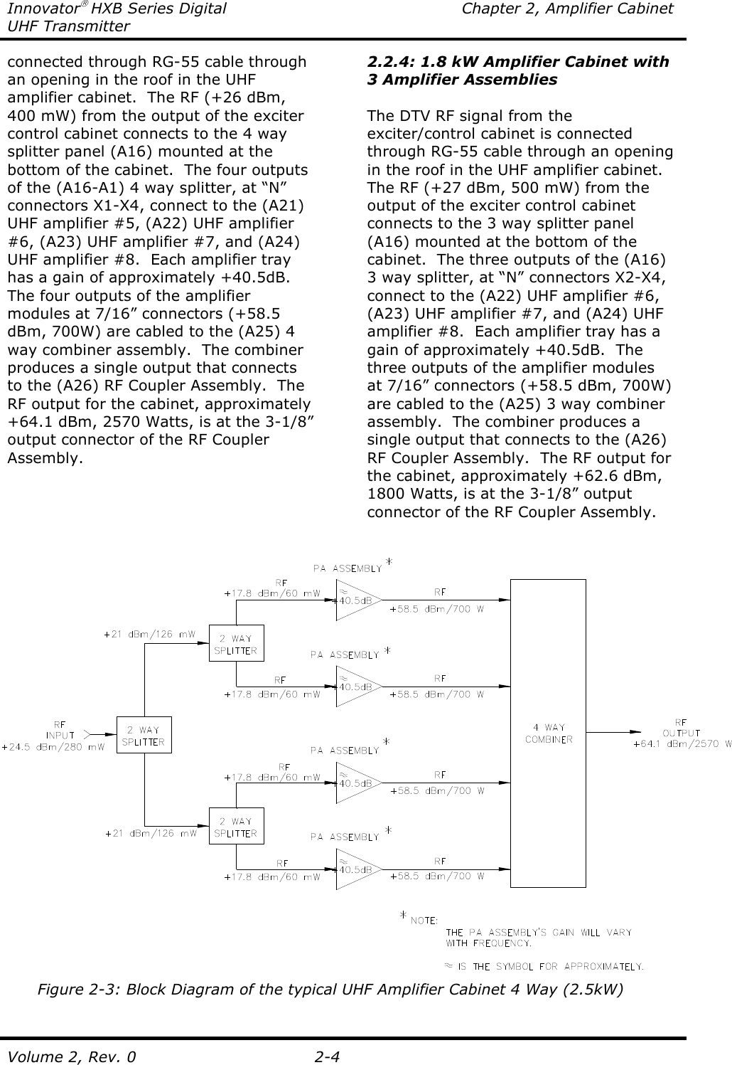


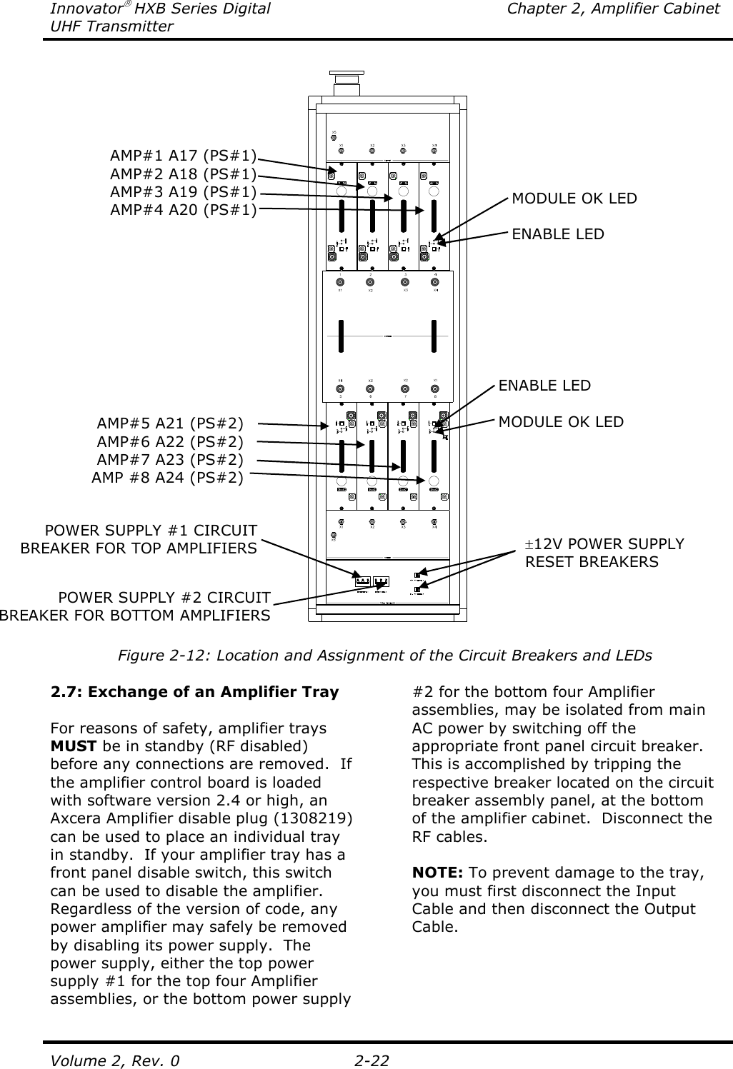

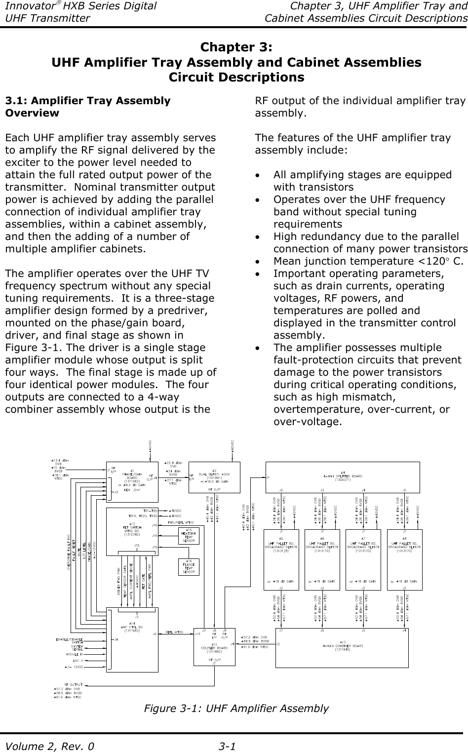
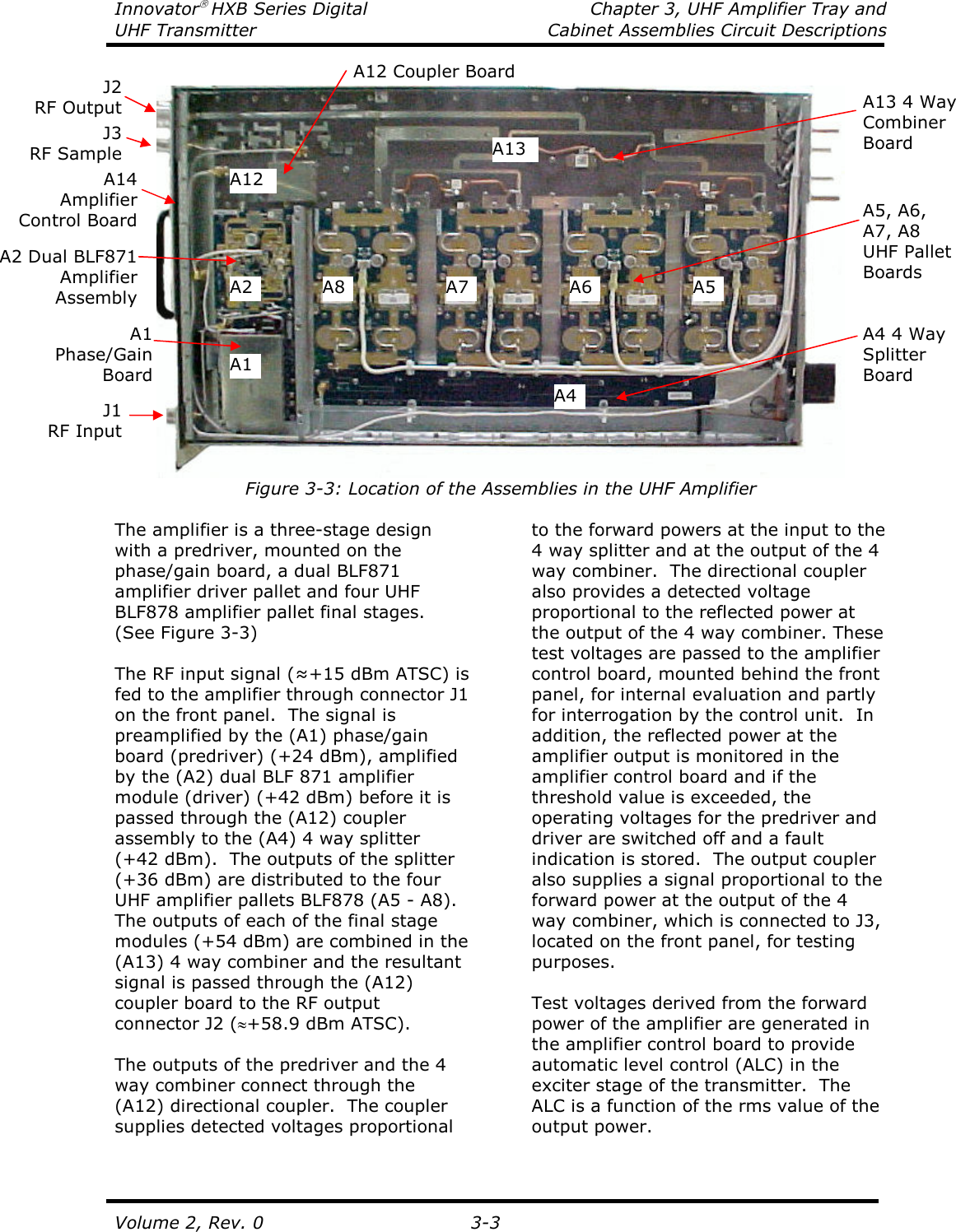
![Innovator HXB Series Digital Chapter 3, UHF Amplifier Tray and UHF Transmitter Cabinet Assemblies Circuit Descriptions Volume 2, Rev. 0 3-2 The paralleling network of the amplifier is arranged so that it continues to operate at reduced power if a module fails. The remaining available power is given by: Prem = Pnom ⋅ ([m - n] / m)2 where: Prem = remaining power Pnom = nominal power m = number of modules n = number of failed modules Figure 3-2: Remaining Power after Failure of Amplifier Modules 3.2: Design of the UHF Amplifier The amplifier tray assembly is designed as a slide-in unit. The mechanical support structure is formed by a finned heat sink on which the individual assemblies are mounted. The amplifier assemblies are listed in Table 3-1. All RF connectors are located on the front panel, while the control and power connectors are mounted at the rear panel. The amplifier control board is mounted vertically behind the front panel. Two LEDs, Module OK and Enable, are mounted on the amplifier control board and are visible through the front panel, indicate the operating status of the amplifier tray. Table 3-1: Assemblies in the UHF Amplifier Tray Position Assembly Remarks A14 Amp Control Board For control, monitoring, and test signal capture A1 Phase/Gain Board Provides phase and gain control of the RF through the tray and also acts as a Predriver, (≈9 dB gain). A2 Dual BLF871 Amplifier Module Assembly Driver power amplifier to the splitter, (≈18 dB gain). A12 Coupler Board Provides Driver forward, final amplifier peak and average forward and reflected power samples. A4 Splitter (1:4) Distributes the RF input from the coupler board to the final amplifier pallets A5 to A8, (≈36 dBm). A5 to A8 UHF Pallet Boards, Broadband BLF878 Four final amplifier boards with ≈18 dB gain and an output of ≈54 dBm. A13 Combiner (4:1) Sums the amplified outputs of the 4 UHF Pallet Boards. (≈58.9 dBm Output) A17 FET Switch/Metering Board Takes the three +48VDC inputs and switches them to the predriver, driver and the amplifier pallets. In addition, the forward and reflected metering samples connect through the board.](https://usermanual.wiki/UBS-Axcera/HU5000BTD.User-manual-4/User-Guide-1210083-Page-37.png)