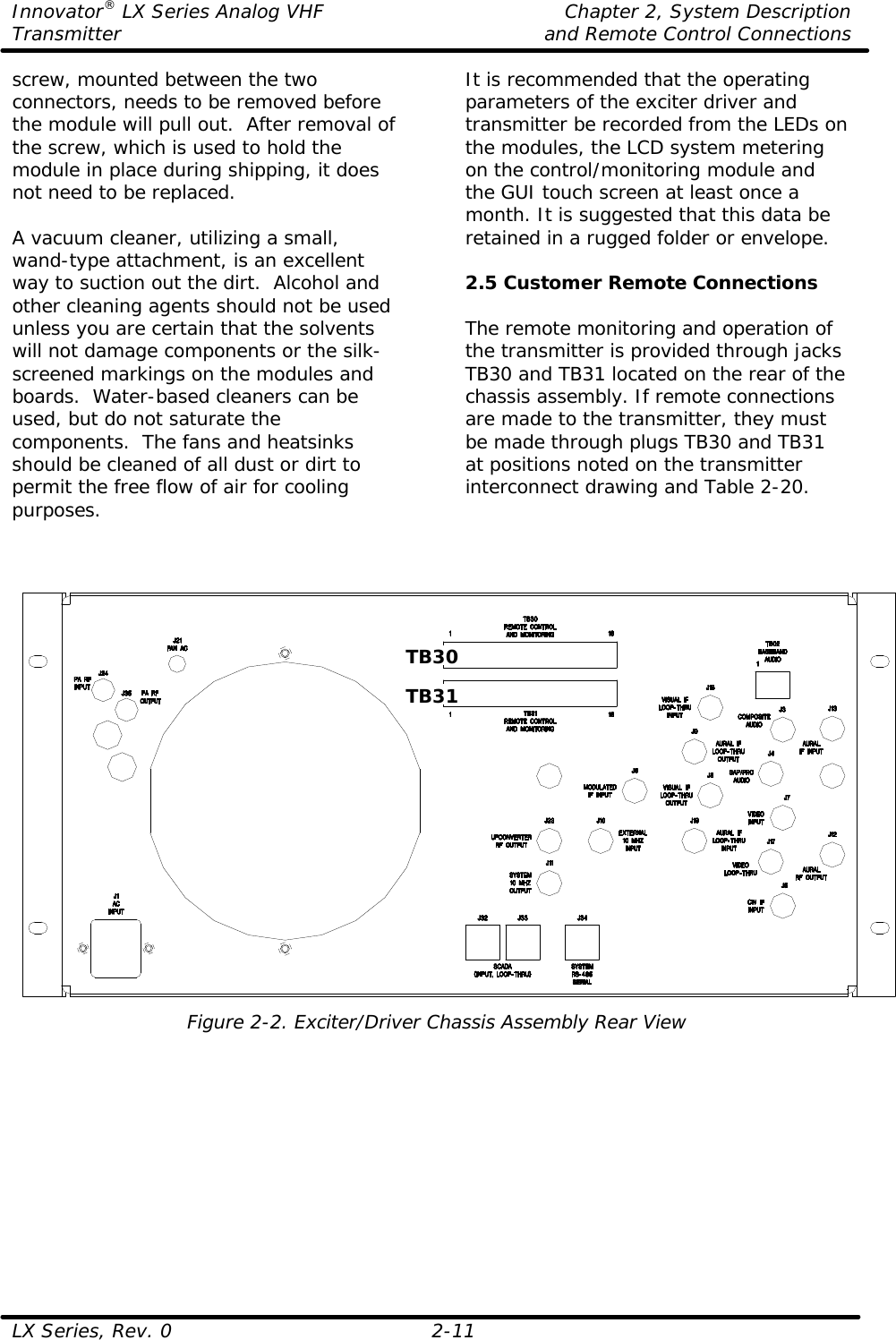
UBS Axcera LLV20AT 20-Watt VHF Low Band Transmitter User Manual Title Page
UBS-Axcera 20-Watt VHF Low Band Transmitter Title Page
UserManual.wiki
>
UBS Axcera
>
LLV20AT User Manual
Compiled User Manual
Navigation menu
Upload a User Manual
Namespaces
Wiki Guide
HTML
PDF
Info
Views
User Manual
Discussion / Help
Navigation
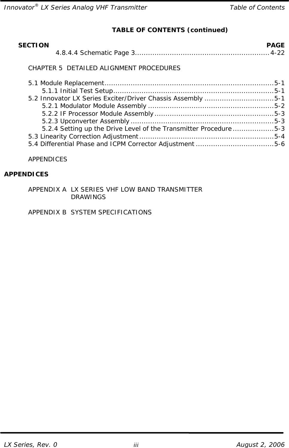
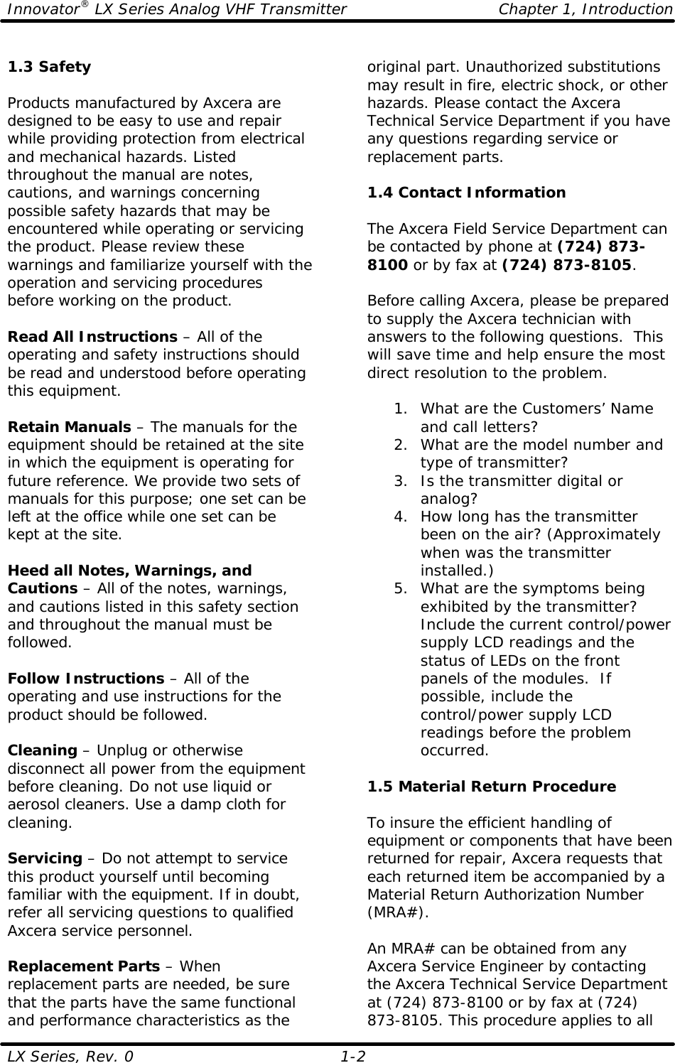
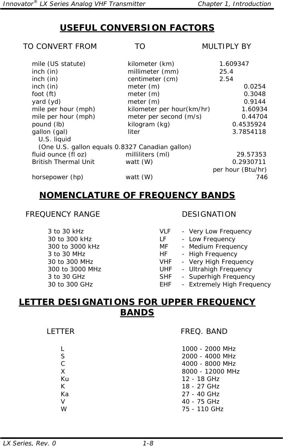
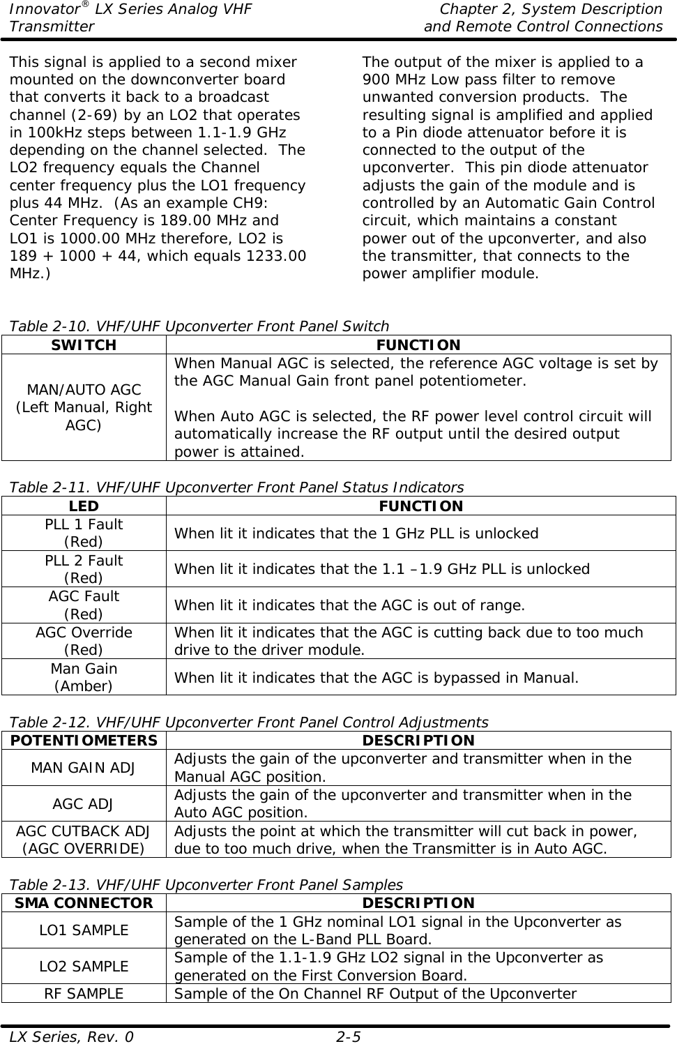
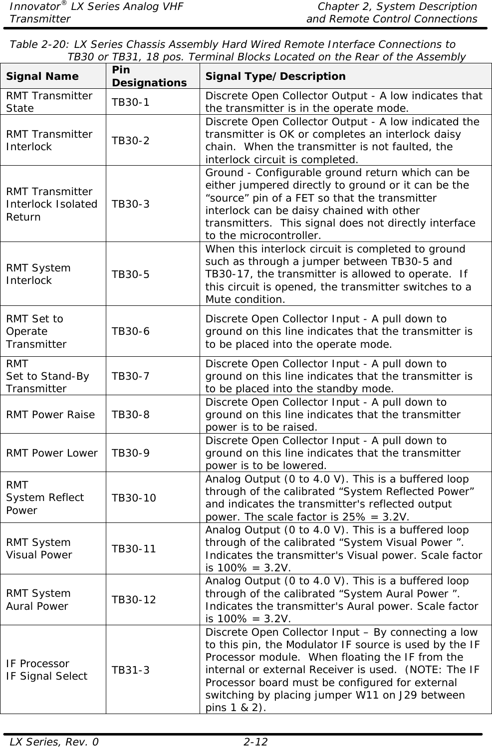
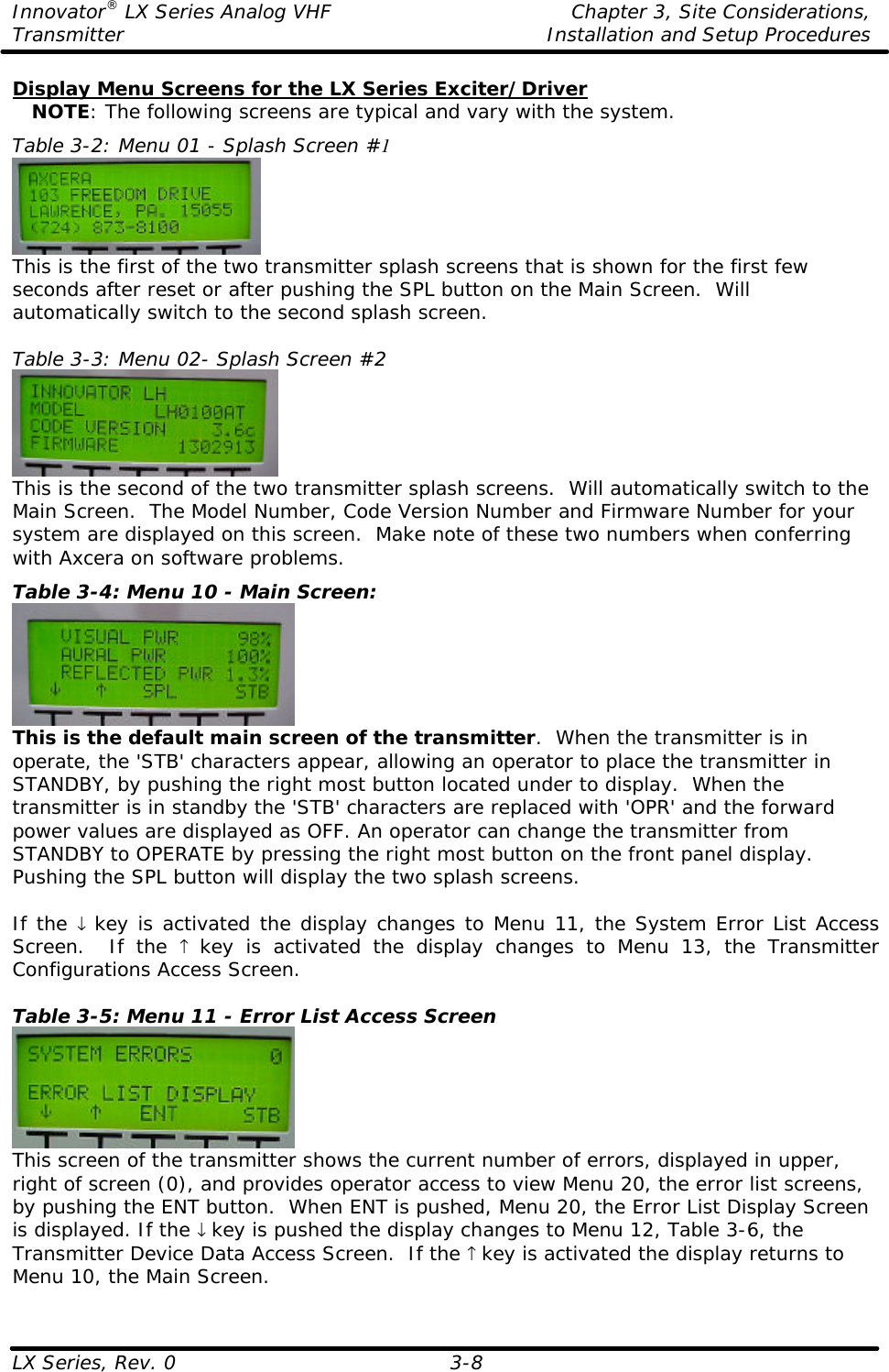
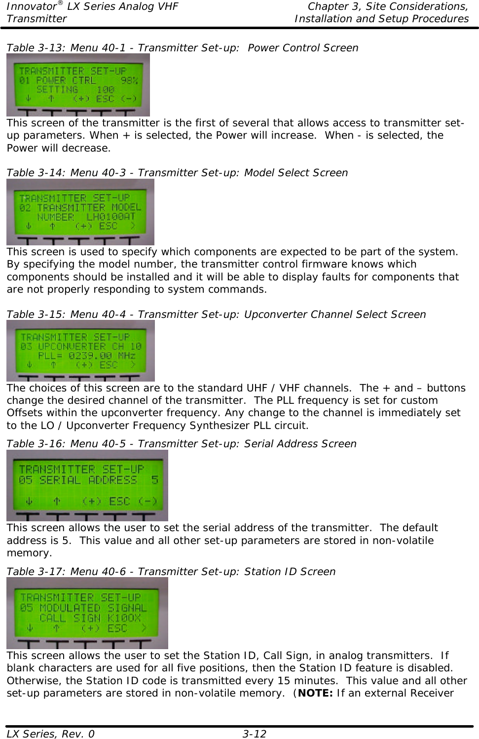
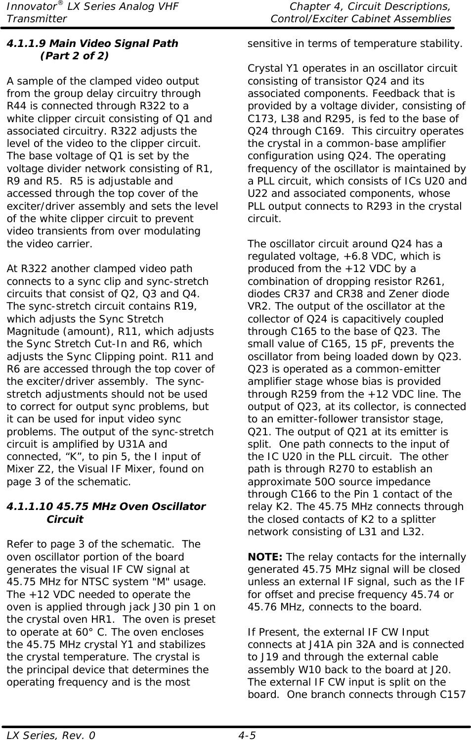
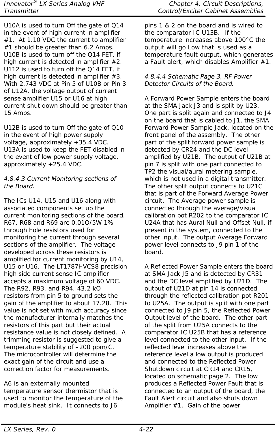
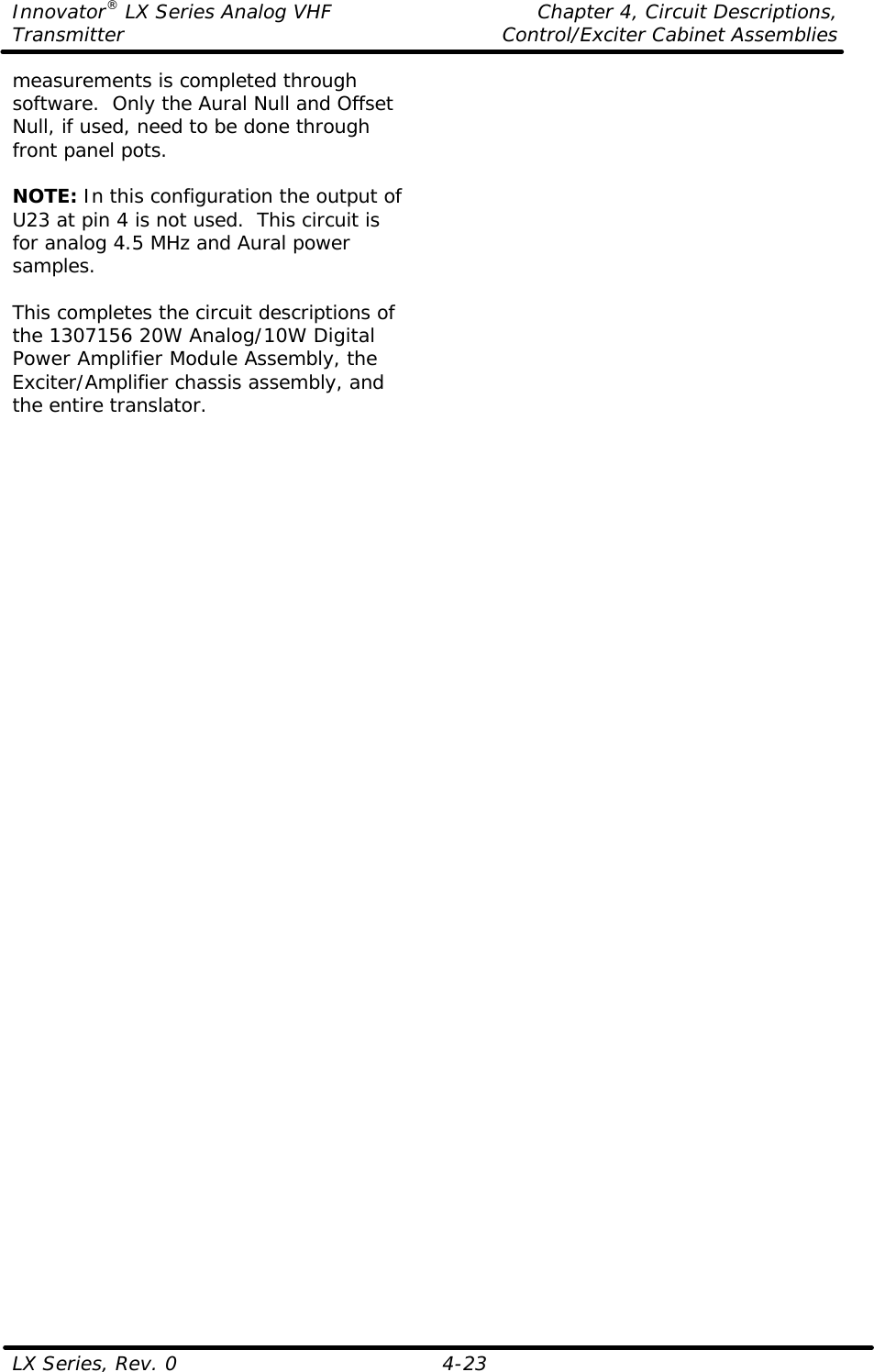
![Innovator® LX Series Analog VHF Transmitter Chapter 1, Introduction LX Series, Rev. 0 1-7 dBm, dBw, dBmV, dBµV, & VOLTAGE EXPRESSED IN WATTS 50 Ohm System WATTS PREFIX dBm dBw dBmV dBµV VOLTAGE 1,000,000,000,000 1 TERAWATT +150 +120 100,000,000,000 100 GIGAWATTS +140 +110 10,000,000,000 10 GIGAWATTS +130 +100 1,000,000,000 1 GIGAWATT +120 + 99 100,000,000 100 MEGAWATTS +110 + 80 10,000,000 10 MEGAWATTS +100 + 70 1,000,000 1 MEGAWATT + 90 + 60 100,000 100 KILOWATTS + 80 + 50 10,000 10 KILOWATTS + 70 + 40 1,000 1 KILOWATT + 60 + 30 100 1 HECTROWATT + 50 + 20 50 + 47 + 17 20 + 43 + 13 10 1 DECAWATT + 40 + 10 1 1 WATT + 30 0 + 77 +137 7.07V 0.1 1 DECIWATT + 20 - 10 + 67 +127 2.24V 0.01 1 CENTIWATT + 10 - 20 + 57 +117 0.707V 0.001 1 MILLIWATT 0 - 30 + 47 +107 224mV 0.0001 100 MICROWATTS - 10 - 40 0.00001 10 MICROWATTS - 20 - 50 0.000001 1 MICROWATT - 30 - 60 0.0000001 100 NANOWATTS - 40 - 70 0.00000001 10 NANOWATTS - 50 - 80 0.000000001 1 NANOWATT - 60 - 90 0.0000000001 100 PICOWATTS - 70 -100 0.00000000001 10 PICOWATTS - 80 -110 0.000000000001 1 PICOWATT - 90 -120 TEMPERATURE CONVERSION °F = 32 + [(9/5) °C] °C = [(5/9) (°F - 32)]](https://usermanual.wiki/UBS-Axcera/LLV20AT/User-Guide-846871-Page-13.png)
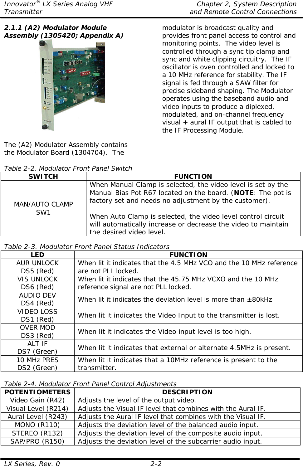
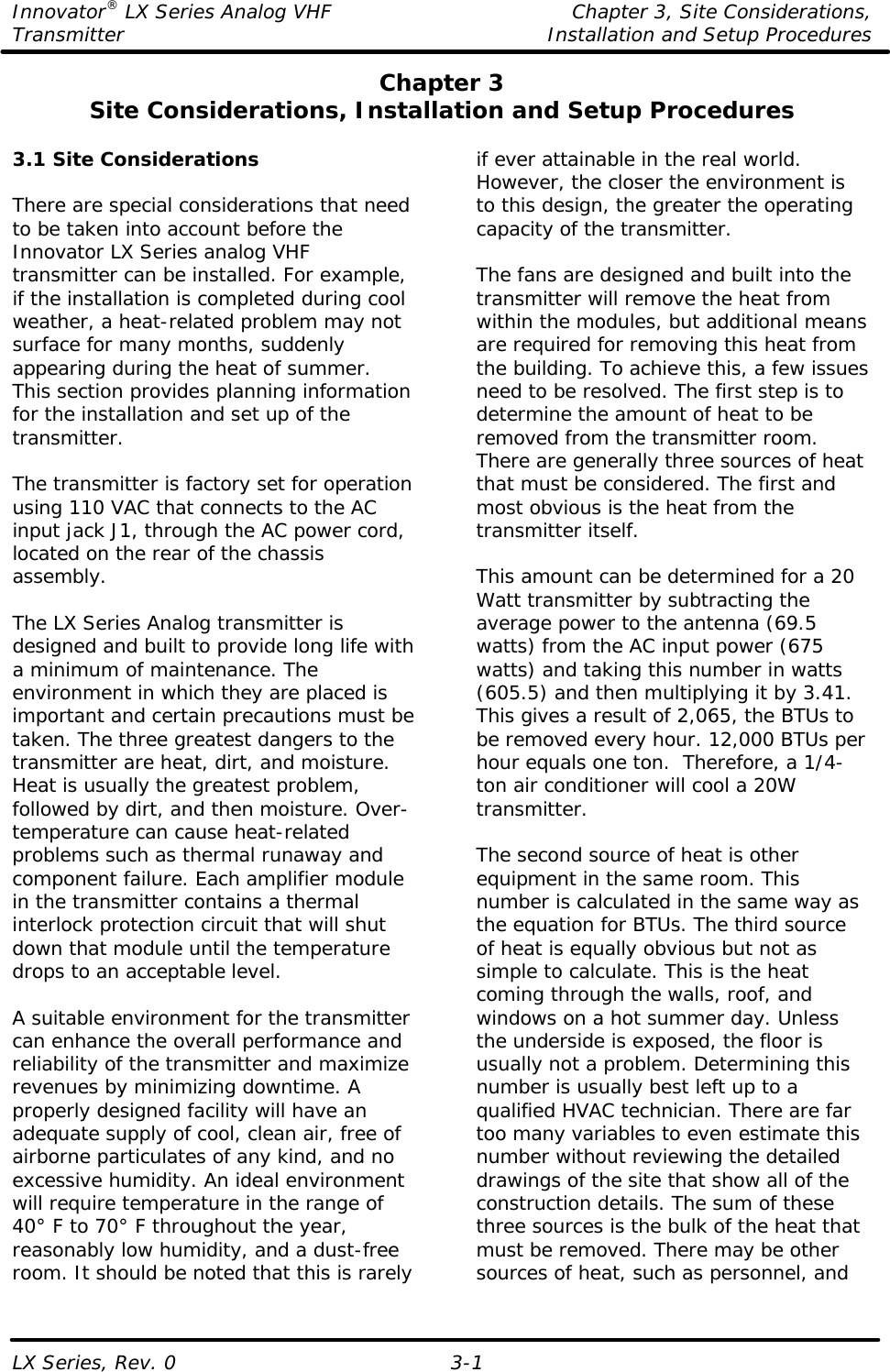
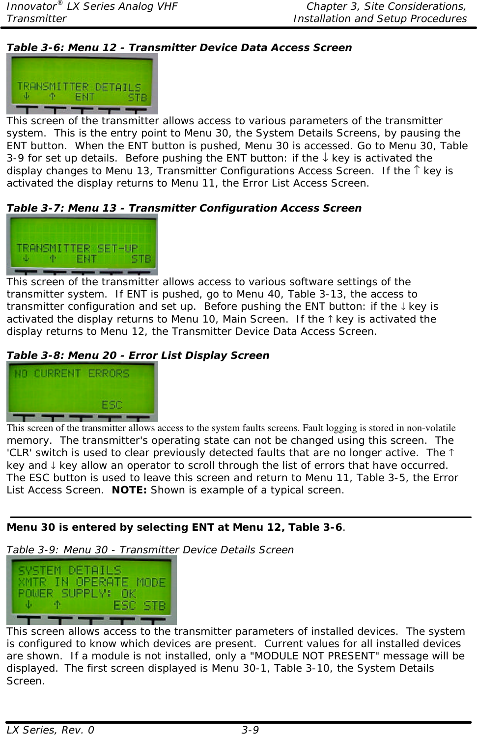
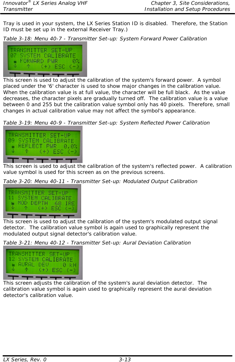
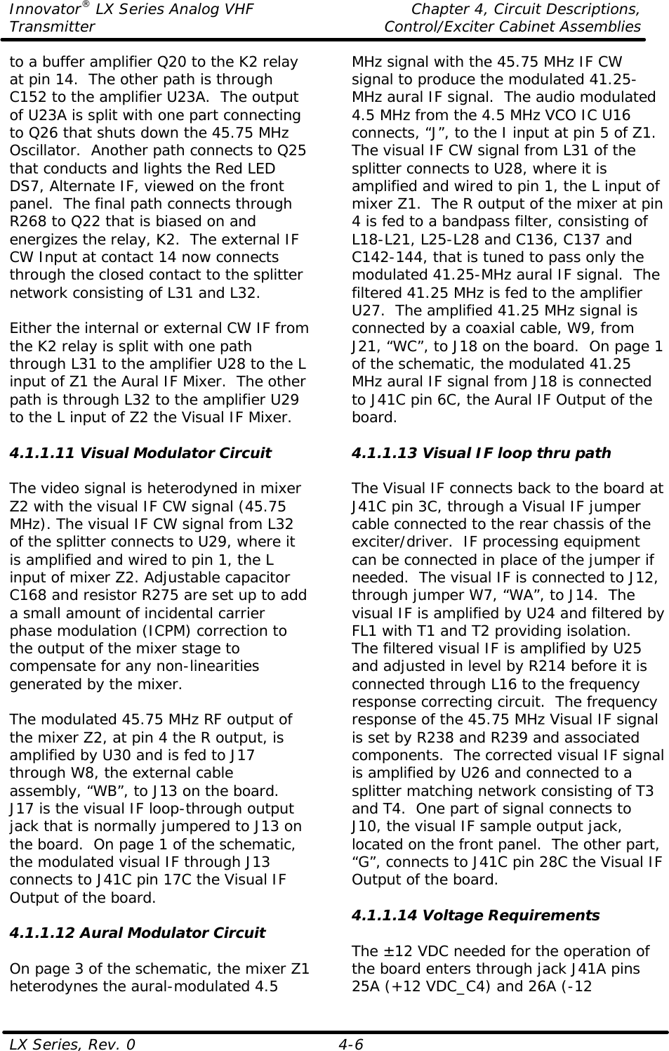
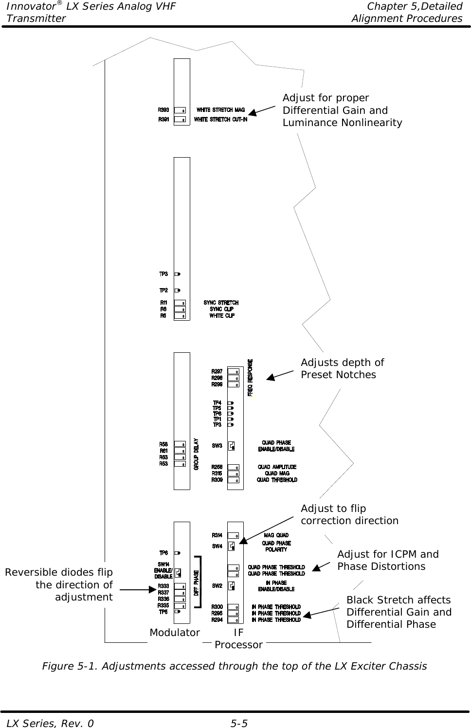
![Innovator® LX Series Analog VHF Chapter 5,Detailed Transmitter Alignment Procedures LX Series, Rev. 0 5-2 adjustments of the drive level to the Power Amplifier and the adjustment of the linearity and phase predistortion to compensate for any nonlinear response of the Power Amplifier. The adjustments are located on the front panel of the IF Processor module. 5.2.1 Modulator Module Assembly The Modulator Assembly has adjustments for video levels and audio modulation levels, and other related parameters. Connect an NTSC baseband video test signal input (1 Vpk-pk) to the transmitter video input jack J7 on the rear of the tray. Jacks J7 and J17 are loop-through connected; the J17 jack can be used as a video source for another transmitter. Connect a baseband audio input (+10 dBm) to the balanced audio input terminal block TB02-1 [+], TB02-2 [-], and TB02-3 [ground] or, if stereo/composite audio is provided, connect it to BNC jack J3, the composite audio input jack. Verify that all LEDs located on the front panel of the Modulator are Green. The following details the meaning of each LED: AURAL UNLOCK (DS5) – Red Indicates that 4.5 MHz Aural IF is unlocked from the 45.75 MHz visual IF. VISUAL UNLOCK (DS6) – Red Indicates that the 45.75 MHz visual IF is unlocked from the 10 MHz reference. AUDIO OVER DEVIATION (DS4) – Red Indicates that the input Audio level is too high. VIDEO LOSS (DS1) – Red Indicates that the input Video level is too low. OVER MODULATION (DS3) – Red Indicates that the input Video level is too high. ALTERNATE IF (DS7) – Red Indicates that an external 45.75 MHz IF is not present to the modulator. 10 MHz PRESENT (DS2) – Red Indicates that an external 10 MHz reference in not present to the modulator. Look at the front panel LCD meter on the Control/Power Supply Module Assembly. Set the LCD screen to the Modulator Details video output level screen, the screen indicates active video from 0 to 1 Vpk-pk. The normal video input level is 1 Vpk-pk on the front panel screen. If this reading is not at the proper level, the overall video level can be changed by adjusting the VIDEO LEVEL control R42 on the front panel of the Modulator to the 1 Vpk-pk level on the front panel screen. Switch the LCD display to the Modulator Details screen that indicates the AUDIO DEVIATION (modulation level) of the signal from 0 to 100 kHz. MONO SET UP: The modulator was factory set for a ±25-kHz deviation with a mono, balanced, audio input of +10 dBm. If the reading is not at the correct level, adjust the MONO Audio Gain pot R110, located on the front panel of the modulator, as necessary, to attain the ±25-kHz deviation on the front panel screen. STEREO SET UP: The modulator was factory set for a ±75-kHz deviation with a stereo, composite, audio input of 1 Vpk-pk. If this reading is not correct, adjust the STEREO Audio Gain pot R132, located on the front panel of the modulator, as necessary, for the ±75-kHz deviation. SECONDARY AUDIO SET UP: NOTE: Remove any stereo or mono audio modulation input to the transmitter during the set up of the secondary audio. The modulator was factory set for a ±15-kHz deviation with a secondary audio input of 1 Vpk-pk. If this reading is not correct, adjust the SAP/PRO Audio Gain pot R150, located on the front panel of](https://usermanual.wiki/UBS-Axcera/LLV20AT/User-Guide-846871-Page-69.png)