UBS Axcera LU1000AT 1000-Watt UHF Transmitter User Manual 379382
UBS-Axcera 1000-Watt UHF Transmitter 379382
Contents
- 1. Title Page Exciter
- 2. Table of Contents Exciter
- 3. Chapter 1 Exciter
- 4. Chapter 2 Exciter
- 5. Chapter 3 Exciter
- 6. Chapter 4 Exciter
- 7. Chapter 5 Exciter
- 8. Appendix Pages Exciter
- 9. Data Sheet Exciter and Amplifier
- 10. Drawings List Exciter
- 11. Title Page External Amplifier
- 12. Table of Contents External Amplifier
- 13. Chapter 1 External Amplifier
- 14. Chapter 2 External Amplifier
- 15. Chapter 3 External Amplifier
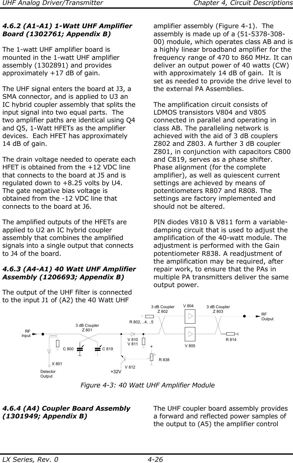
- 16. Chapter 4 External Amplifier
- 17. Chapter 5 External Amplifier
- 18. Appendix Pages External Amplifier
- 19. Drawings List External Amplifier
Chapter 4 Exciter