UBS Axcera LU10AL 10-Watt UHF Translator User Manual TITLE PAGE
UBS-Axcera 10-Watt UHF Translator TITLE PAGE
UserManual.wiki
>
UBS Axcera
>
LU10AL User Manual
Compiled User Manual
Navigation menu
Upload a User Manual
Namespaces
Wiki Guide
HTML
PDF
Info
Views
User Manual
Discussion / Help
Navigation
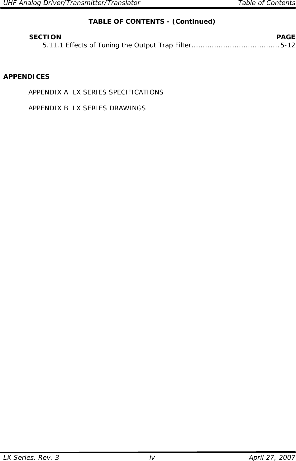
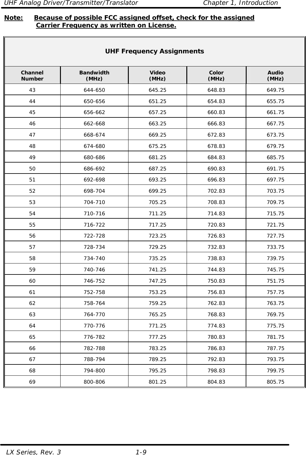
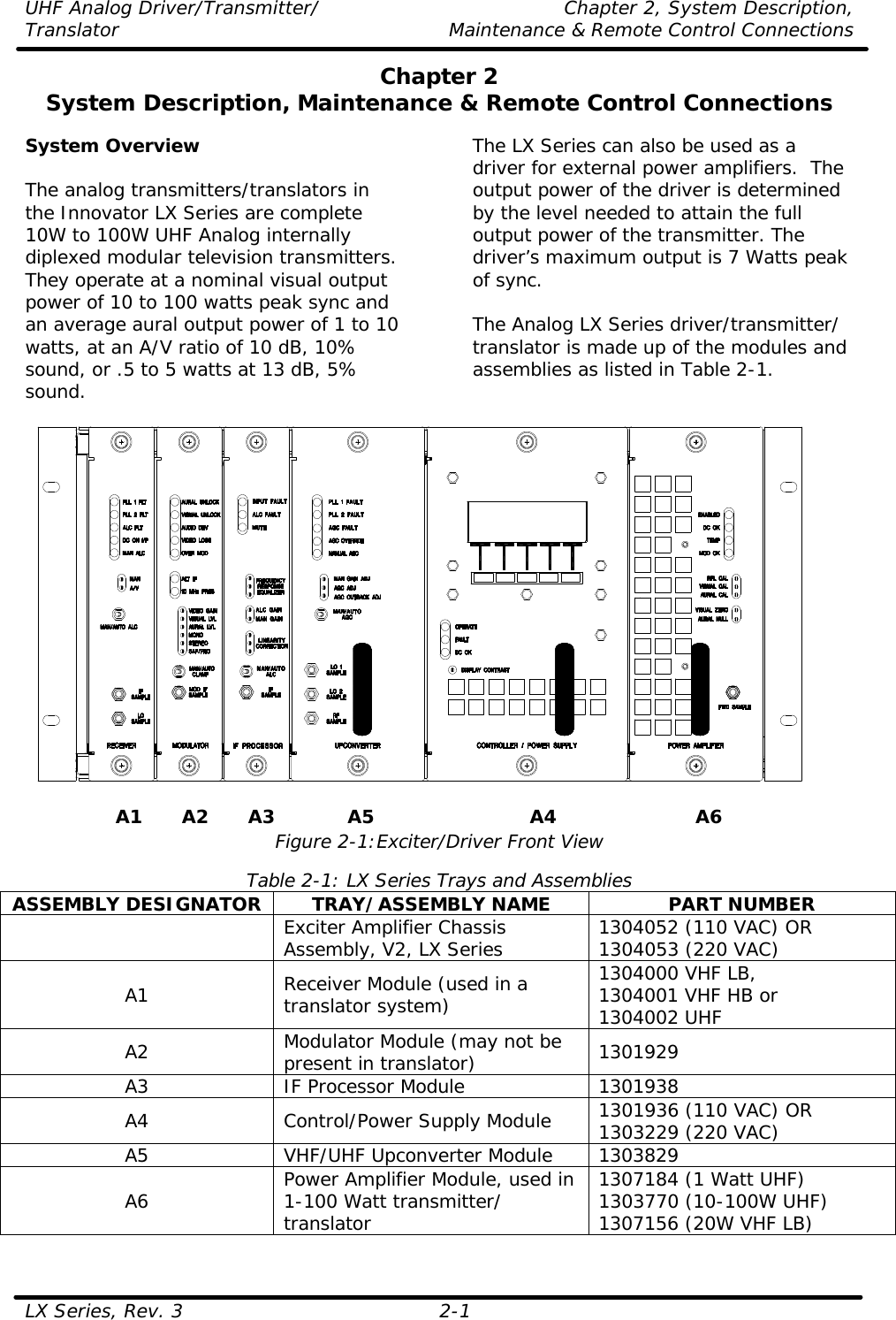
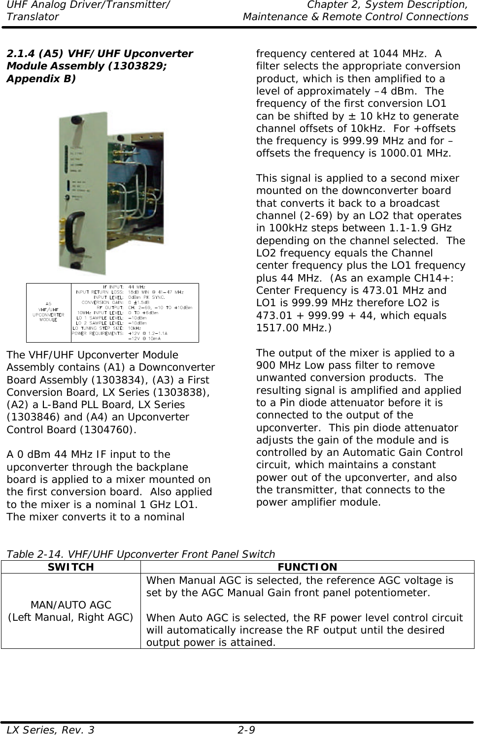
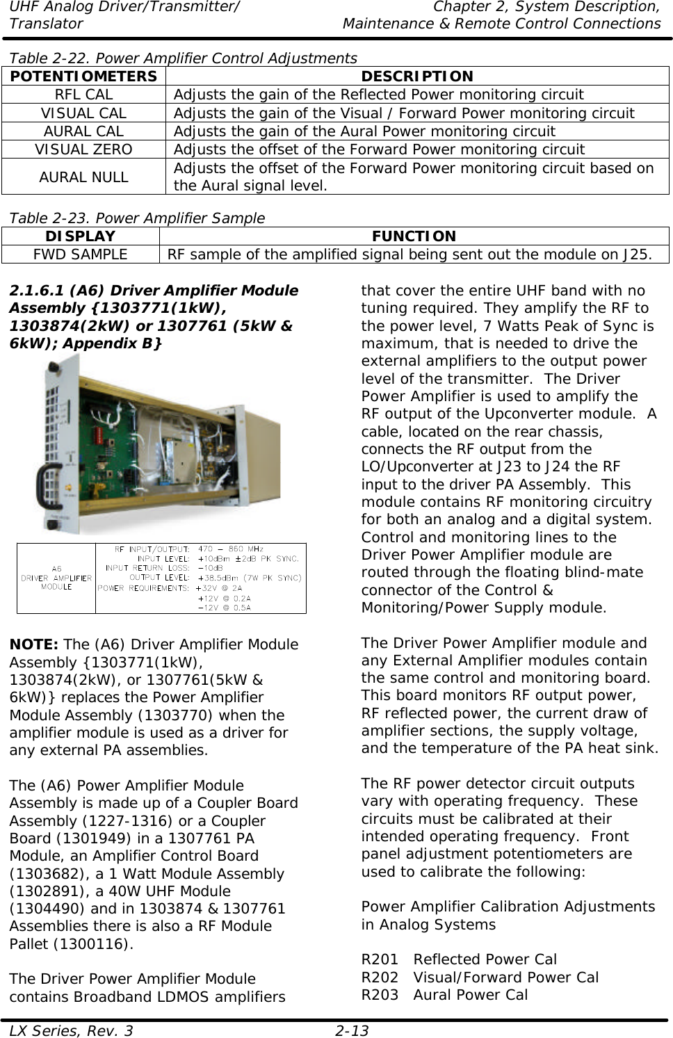
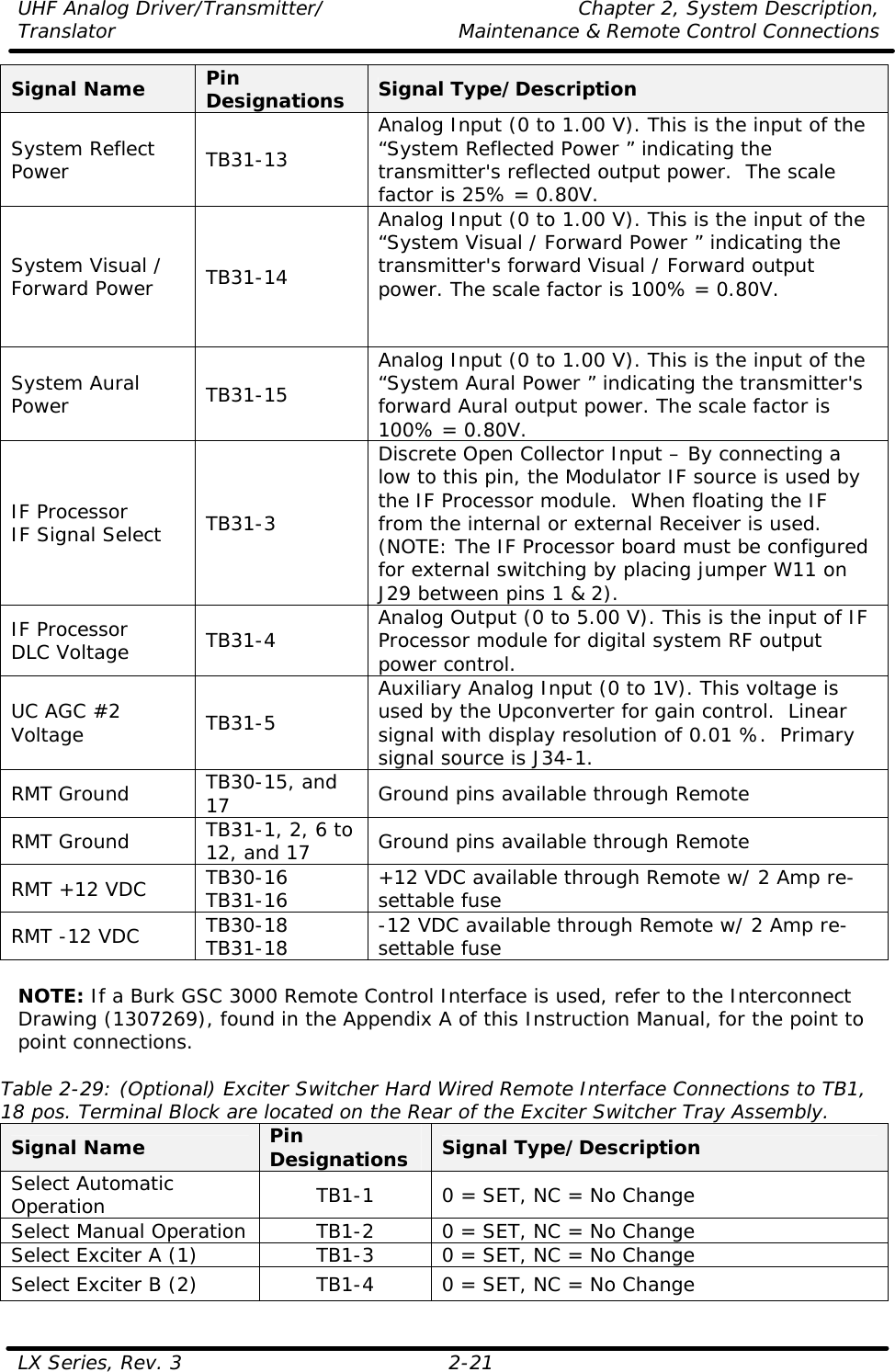
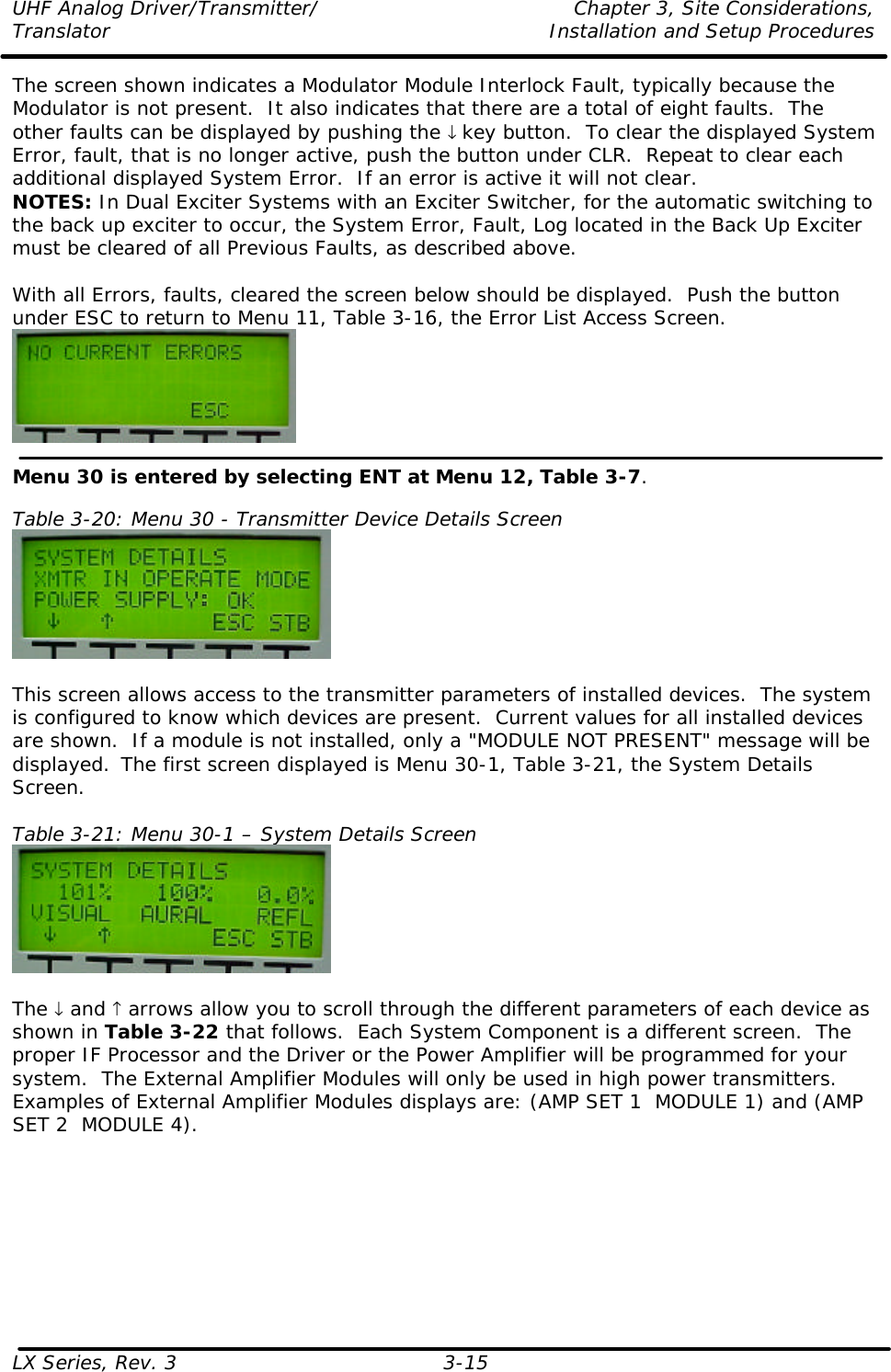
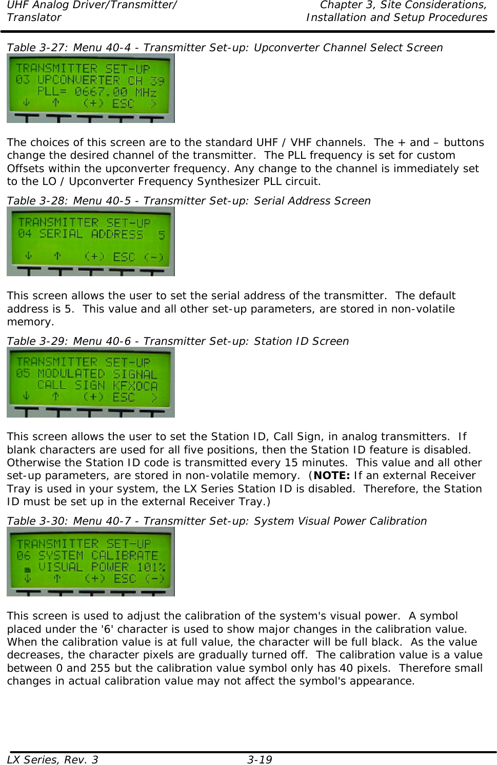
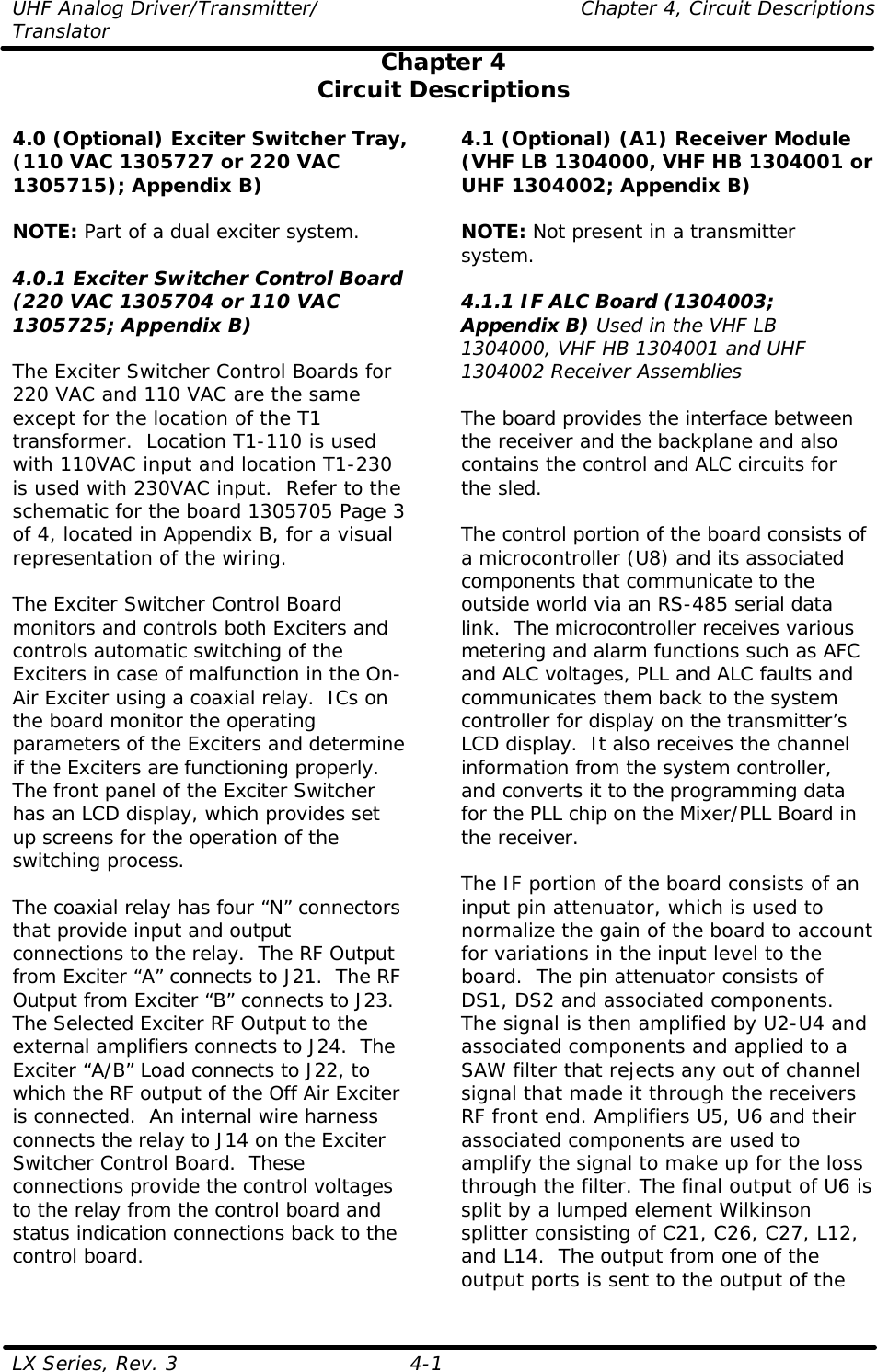
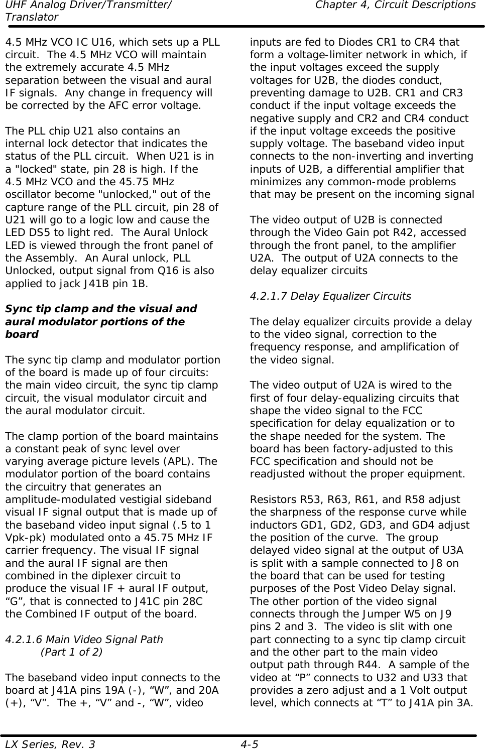
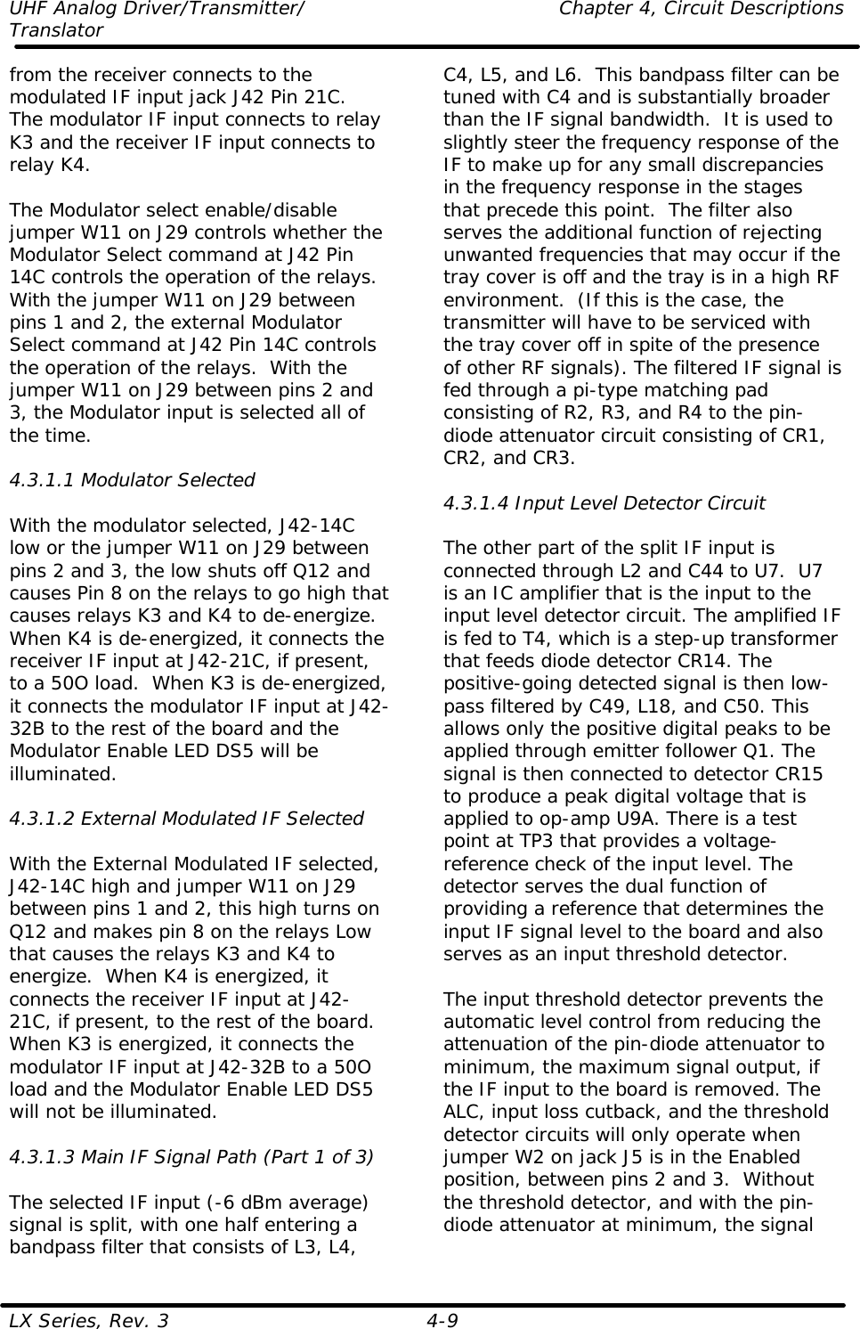
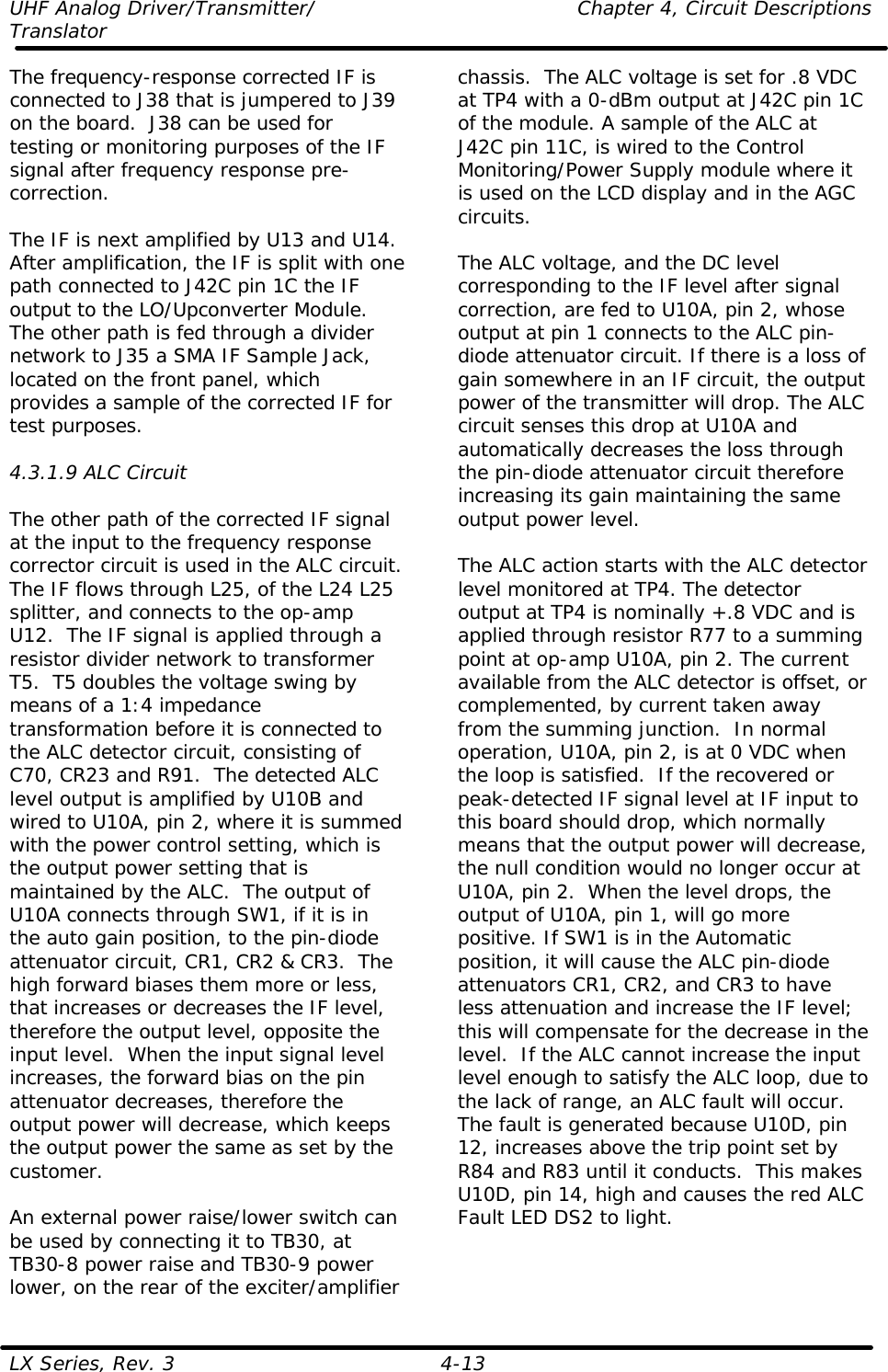
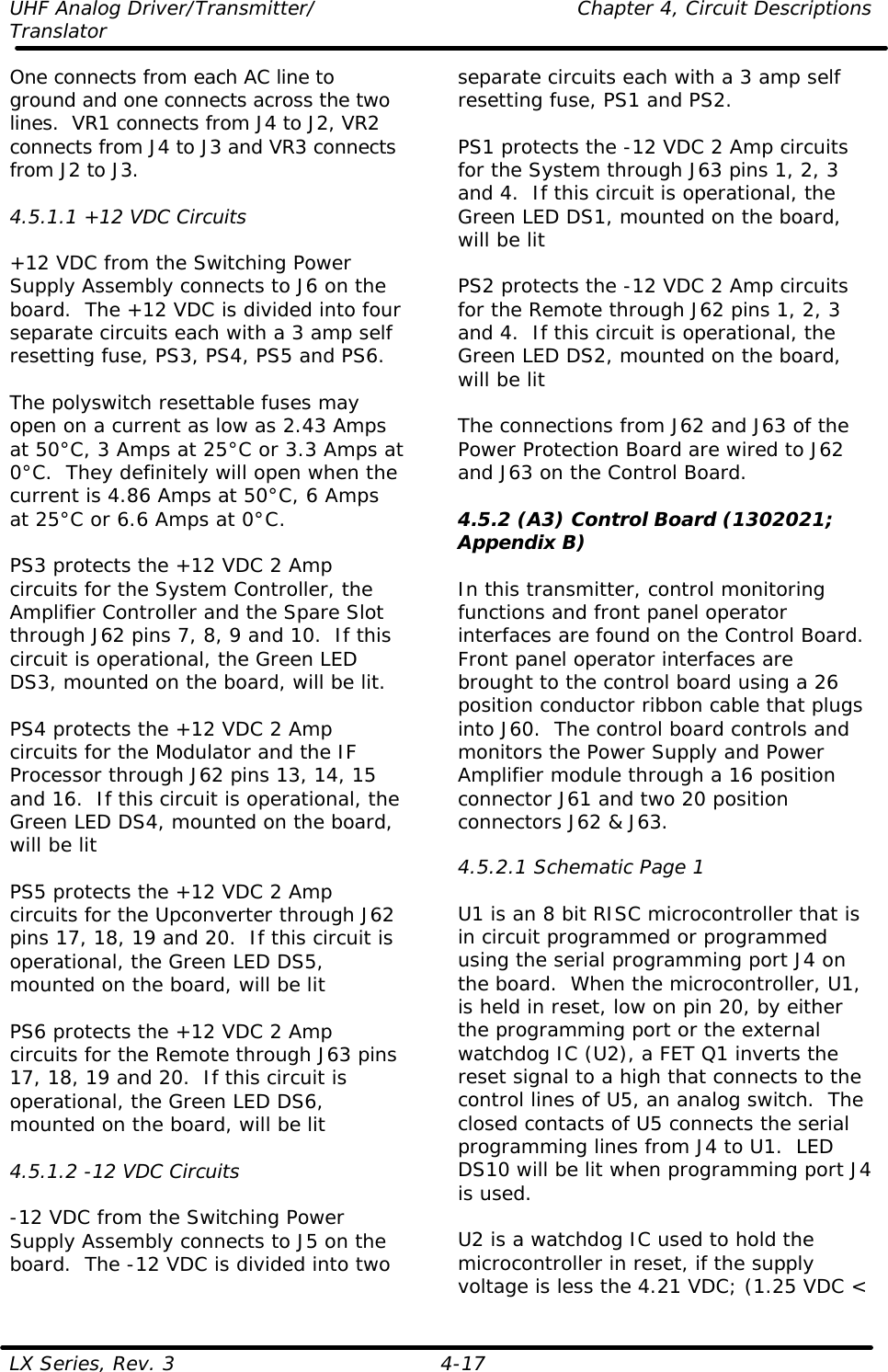
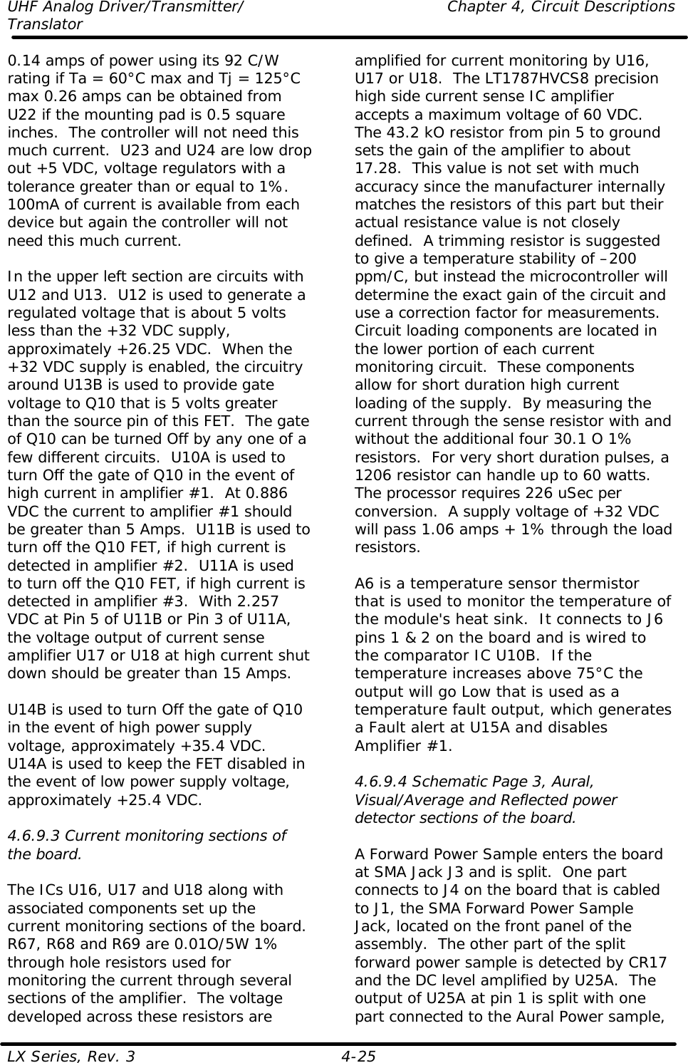
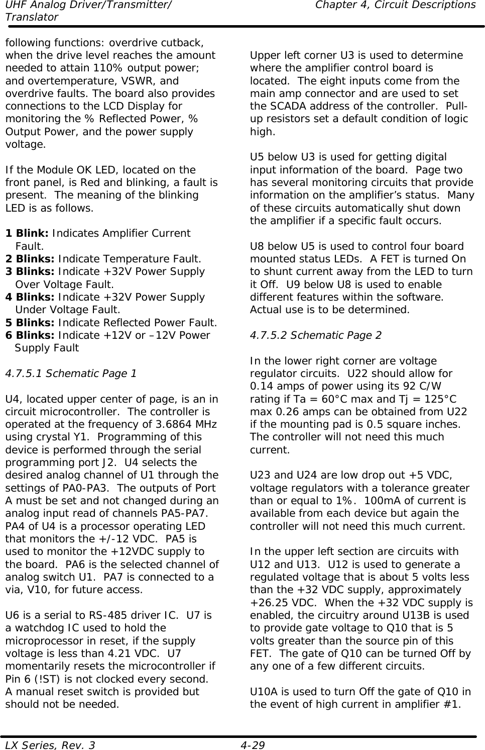
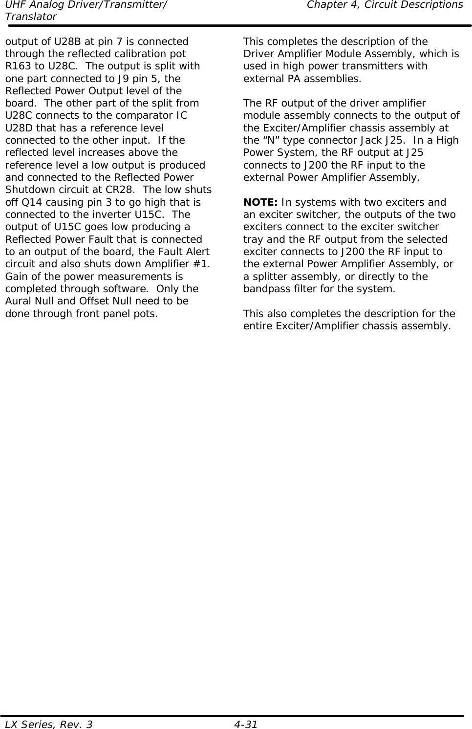
![UHF Analog Driver/Transmitter/Translator Chapter 1, Introduction LX Series, Rev. 3 1-10 dBm, dBw, dBmV, dBµV, & VOLTAGE EXPRESSED IN WATTS 50 Ohm System WATTS PREFIX dBm dBw dBmV dBµV VOLTAGE 1,000,000,000,000 1 TERAWATT +150 +120 100,000,000,000 100 GIGAWATTS +140 +110 10,000,000,000 10 GIGAWATTS +130 +100 1,000,000,000 1 GIGAWATT +120 + 99 100,000,000 100 MEGAWATTS +110 + 80 10,000,000 10 MEGAWATTS +100 + 70 1,000,000 1 MEGAWATT + 90 + 60 100,000 100 KILOWATTS + 80 + 50 10,000 10 KILOWATTS + 70 + 40 1,000 1 KILOWATT + 60 + 30 100 1 HECTROWATT + 50 + 20 50 + 47 + 17 20 + 43 + 13 10 1 DECAWATT + 40 + 10 1 1 WATT + 30 0 + 77 +137 7.07V 0.1 1 DECIWATT + 20 - 10 + 67 +127 2.24V 0.01 1 CENTIWATT + 10 - 20 + 57 +117 0.707V 0.001 1 MILLIWATT 0 - 30 + 47 +107 224mV 0.0001 100 MICROWATTS - 10 - 40 0.00001 10 MICROWATTS - 20 - 50 0.000001 1 MICROWATT - 30 - 60 0.0000001 100 NANOWATTS - 40 - 70 0.00000001 10 NANOWATTS - 50 - 80 0.000000001 1 NANOWATT - 60 - 90 0.0000000001 100 PICOWATTS - 70 -100 0.00000000001 10 PICOWATTS - 80 -110 0.000000000001 1 PICOWATT - 90 -120 TEMPERATURE CONVERSION °F = 32 + [(9/5) °C] °C = [(5/9) (°F - 32)]](https://usermanual.wiki/UBS-Axcera/LU10AL/User-Guide-789780-Page-18.png)
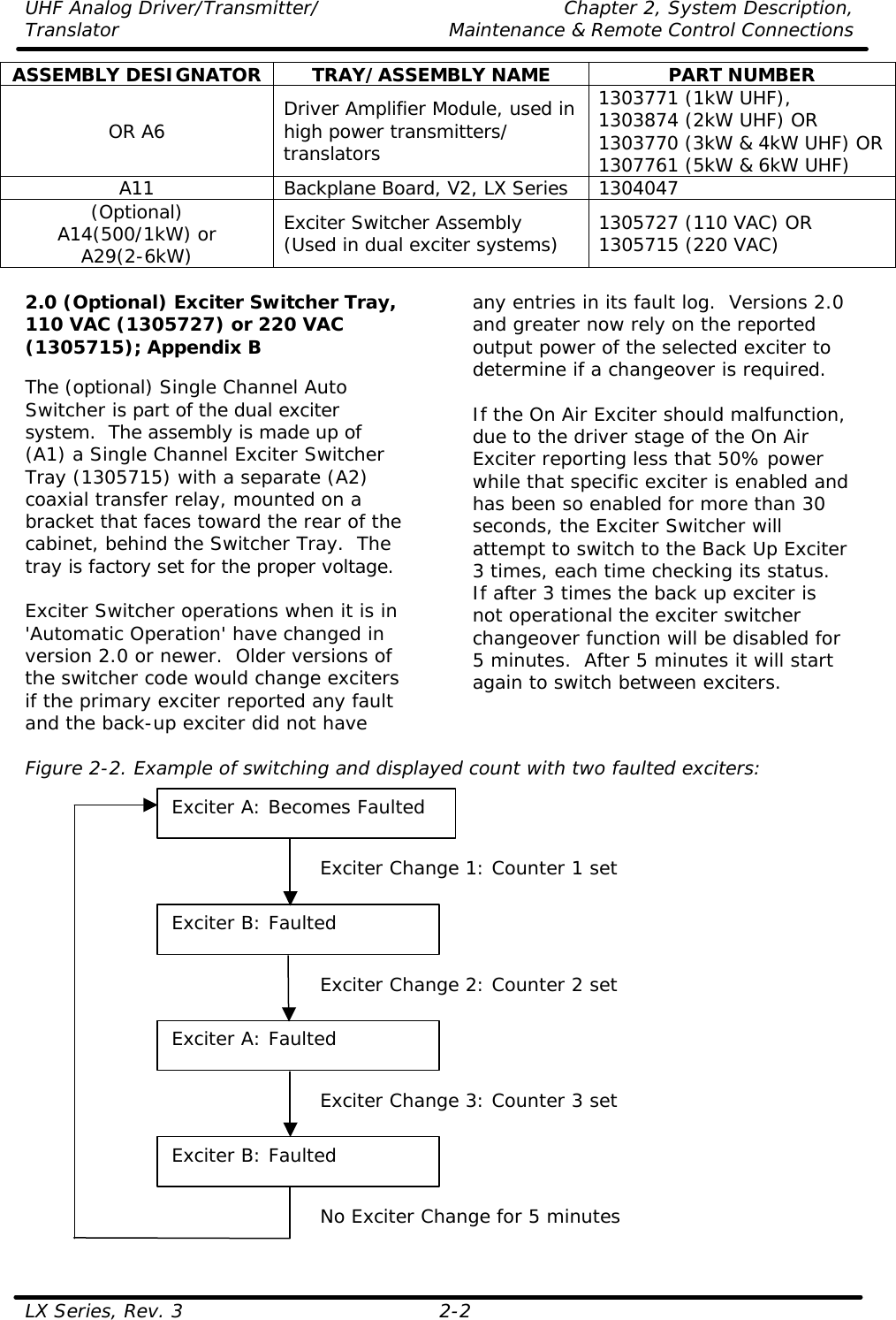
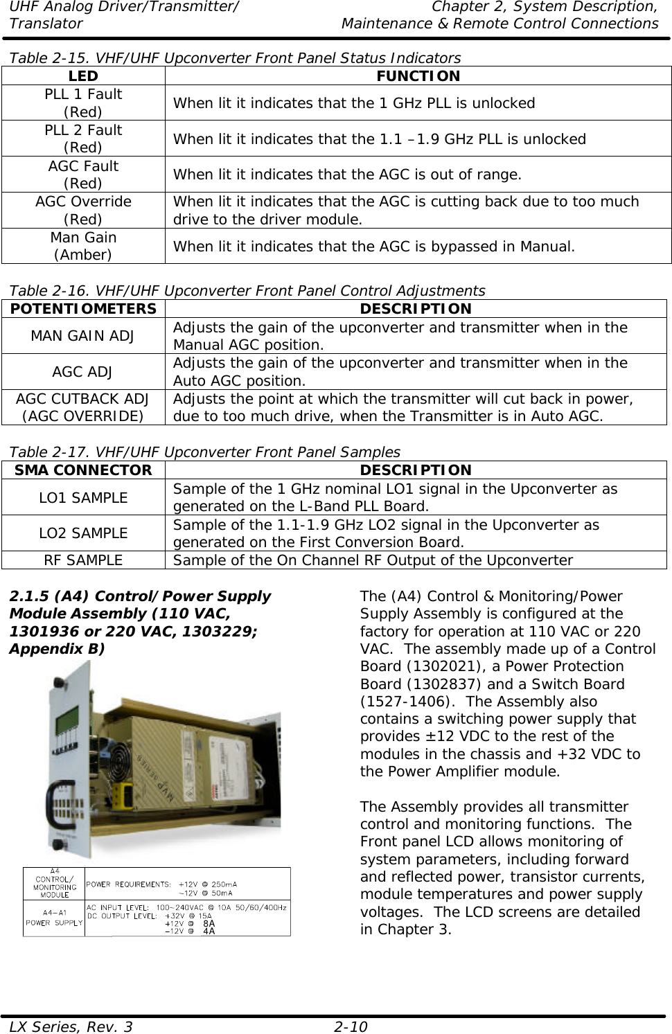
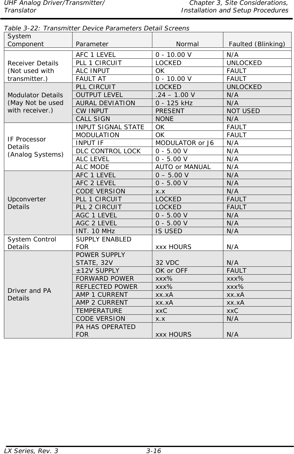
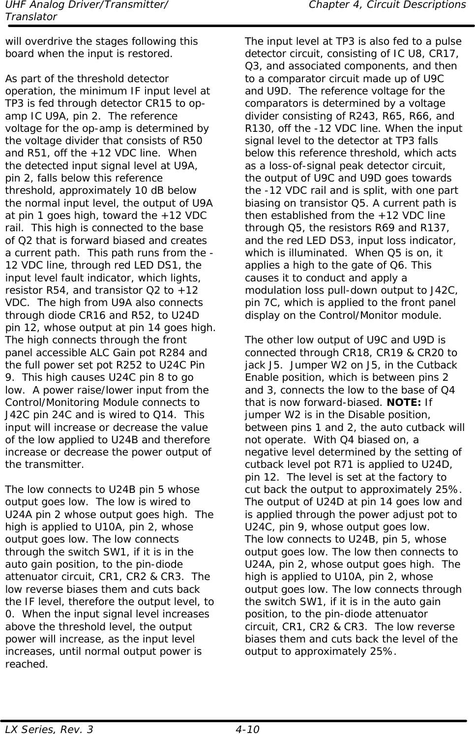
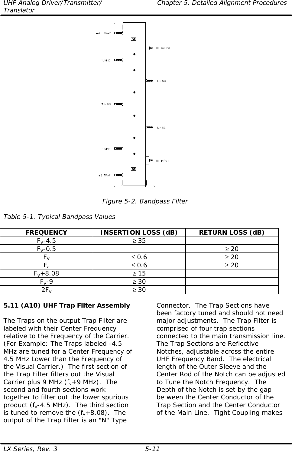
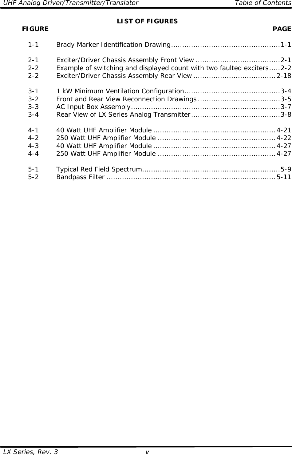
![UHF Analog Driver/Transmitter/ Chapter 5, Detailed Alignment Procedures Translator LX Series, Rev. 3 5-2 factory with the readings on each of the modules. The readings should be very similar. If a reading is way off, the problem is likely to be in that module. Switch On the main AC for the system. 5.2 LX Series Exciter/Amplifier Chassis Assembly The transmitter operates using baseband audio and video inputs. The translator uses the on channel UHF input. NOTE: In systems that contain two exciters with an exciter switcher, both exciters must have audio and video inputs. Each exciter should be operated one at a time using the following procedure by first selecting Exciter A as the On Air exciter then selecting Exciter B as the On Air exciter. The Exciter Switcher must be in the manual mode. On the LCD Display, located on the Controller/Power Supply Module, in Transmitter Set-Up, push the right button to switch the transmitter to Operate, STB will be displayed. The check of and the setup of the Audio and Video input levels are completed using the LCD Display and the front panel adjustments on the Modulator assembly. The level of the RF output includes adjustments of the drive level to the Power Amplifier and the adjustment of the linearity and phase predistortion to compensate for any nonlinear response of the Power Amplifier. The adjustments are located on the front panel of the IF Processor module. 5.2.1 (Optional) Receiver Module Assembly NOTE: Not present in a Transmitter system. Connect an on channel RF input to J12 the receiver RF input jack on the rear of exciter/driver assembly. Verify that all LEDs located on the front panel of the Receiver are Green. The following details the meaning of each LED: PLL 1 Fault (DS6) - Displays the status of the Local oscillator PLL PLL 2 Fault (DS8) - Displays status of optional input frequency correcting PLL DC on center conductor (DS4) - Displays whether or not DC is applied to the RF input center conductor* *Caution: Do not hook up the RF input to any test equipment with the DC bias applied. Always move the jumper W1 on J2 on the UHF or VHF Preamplifier board to the Bias off position, between pins 2 & 3, to prevent possible damage to the test equipment. 5.2.2 Modulator Module Assembly NOTE: May not present in a Translator system. The Modulator Assembly has adjustments for video levels and audio modulation levels, and other related parameters. Connect an NTSC baseband video test signal input (1 Vpk-pk) to the transmitter video input jack J7 on the rear of the exciter. Jacks J7 and J17 are loop-through connected; the J17 jack can be used as a video source for another transmitter. Connect a baseband audio input (+10 dBm) to the balanced audio input terminal block TB02-1 [+], TB02-2 [-], and TB02-3 [ground] or, if stereo/composite audio is provided, connect it to BNC jack J3, the composite audio input jack. Verify that all LEDs located on the front panel of the Modulator are Green. The following details the meaning of each LED:](https://usermanual.wiki/UBS-Axcera/LU10AL/User-Guide-789780-Page-98.png)