UBS Axcera LU10AT 10-Watt UHF Transmitter User Manual TITLE PAGE
UBS-Axcera 10-Watt UHF Transmitter TITLE PAGE
Compiled User Manual LU10AT

INSTRUCTION MANUAL
Innovator
LX Series
UHF Analog
Driver
AXCERA, LLC
103 FREEDOM DRIVE P.O. BOX 525 LAWRENCE, PA 15055-0525 USA
(724) 873-8100 • FAX (724) 873-8105
www.axcera.com • info@axcera.com

UHF Analog Driver/Transmitter/Translator Table of Contents
LX Series, Rev. 3 April 27, 2007
i
TABLE OF CONTENTS
CHAPTER 1 INTRODUCTION
SECTION PAGE
1.1 Manual Overview...................................................................................1-1
1.2 Assembly Designators............................................................................1-1
1.3 Safety..................................................................................................1-2
1.4 Contact Information ......................................................................... 1-2
1.5 Material Return Procedure ......................................................................1-2
1.6 Limited One Year Warranty for Axcera Products........................................1-3
CHAPTER 2 SYSTEM DESCRIPTION, MAINTENANCE
& REMOTE CONTROL CONNECTIONS
System Overview..................................................................................2-1
2.0 (Optional) Exciter Switcher Tray.............................................................2-2
2.1 Exciter/Amplifier Chassis Assembly ........................................................2-3
2.1.1 Receiver Module (not used in a transmitter system).........................2-3
2.1.2 Modulator Module (may not be used in a translator system) .............2-5
2.1.3 IF Processor Module .....................................................................2-7
2.1.4 VHF/UHF Upconverter Module........................................................2-9
2.1.5 Control & Monitoring/Power Supply Module...................................2-10
2.1.6 Exciter PA Module used in 1-100W Xmitters. or Drvrs above 2kW....2-11
2.1.6.1 Driver Amplifier Module, used with 1kW or 2kW transmitters.2-13
2.1.7 RF Output Assemblies.................................................................2-15
2.2 Control and Status...............................................................................2-15
2.2.1 Front Panel LCD Display Screen ...................................................2-15
2.3 System Operation................................................................................2-15
2.3.1 Principles of Operation................................................................2-15
2.4 Maintenance .......................................................................................2-18
2.5 Customer Remote Connections....................................................... 2-18
CHAPTER 3 SITE CONSIDERATIONS, INSTALLATION AND SETUP PROCEDURES
3.1 Site Considerations................................................................................3-1
3.2 Unpacking the Chassis w/Modules, bandpass and trap filters......................3-5
3.3 Installing the Chassis w/Modules and filters..............................................3-5
3.4 AC Input...............................................................................................3-6
3.5 Setup and Operation..............................................................................3-7
3.5.1 Input Connections........................................................................3-7
3.5.2 Initial Turn On .............................................................................3-9
3.5.2.1 (Optional) Receiver Module LEDs on Front Panel.....................3-9
3.5.2.2 Modulator Module LEDs on Front Panel ..................................3-9
3.5.2.3 IF Processor Module LEDs on Front Panel...............................3-9
3.5.2.4 VHF/UHF Upconverter Module LEDs on Front Panel ...............3-10
3.5.2.5 Controller Module LEDs on Front Panel ................................3-10
3.5.2.6 Power Amplifier or Driver Module LEDs on Front Panel ..........3-10
3.5.3 Front Panel Screens for the (Optional) Exciter Switcher Assembly....3-10
3.5.4 Front Panel Screens for the Exciter/Amplifier Chassis Assembly.......3-13
3.5.5 Operation Procedure...................................................................3-22
CHAPTER 4 CIRCUIT DESCRIPTIONS
4.0 (Optional) Exciter Switcher Tray (Used with dual exciter system) ...............4-1

UHF Analog Driver/Transmitter/Translator Table of Contents
LX Series, Rev. 3 April 27, 2007
ii
TABLE OF CONTENTS - (Continued)
SECTION PAGE
4.0.1 Exciter Switcher Control Board.......................................................4-1
4.1 (Optional) Receiver Module (not used in a transmitter system)...................4-1
4.1.1 IF ALC Board ...............................................................................4-1
4.1.2 UHF or VHF Mixer/PLL Board .........................................................4-2
4.1.3 UHF, VHF LB or VHF HB Preamplifier Board.....................................4-2
4.2 Modulator Module (may not be used in a translator system) ......................4-3
4.2.1 Analog Modulator Board................................................................4-3
4.2.1.1 Mono, Balanced Audio Input.................................................4-3
4.2.1.2 Stereo, Composite Audio Input.............................................4-4
4.2.1.3 SAP/PRO, Subcarrier Audio Input..........................................4-4
4.2.1.4 Audio Modulation of the 3.4 MHz VCO ..................................4-4
4.2.1.5 Phase Lock Loop (PLL) Circuit...............................................4-4
4.2.1.6 Main Video Signal Path (Part 1 of 2)......................................4-5
4.2.1.7 Delay Equalizer Circuits .......................................................4-5
4.2.1.8 Sync Tip Clamp Circuit.........................................................4-6
4.2.1.9 Main Video Signal Path (Part 2 of 2)......................................4-6
4.2.1.10 45.75 MHz Oven Oscillator Circuit .......................................4-6
4.2.1.11 Visual Modulator Circuit .....................................................4-7
4.2.1.12 Aural Modulator Circuit ......................................................4-7
4.2.1.13 Combining the 45.75 MHz & 41.25 MHz IF Signals................4-8
4.2.1.14 Voltage Requirements........................................................4-8
4.3 IF Processor Module...............................................................................4-8
4.3.1 IF Processor Board .......................................................................4-8
4.3.1.1 Modulator Selected..............................................................4-9
4.3.1.2 External Modulated IF Selected.............................................4-9
4.3.1.3 Main IF Signal Path (Part 1 of 3)...........................................4-9
4.3.1.4 Input Level Detector Circuit..................................................4-9
4.3.1.5 Pin-Diode Attenuator Circuit...............................................4-11
4.3.1.6 Main IF Signal Path (Part 2 of 3).........................................4-11
4.3.1.7 Amplitude and Phase Pre-Correction Circuits........................4-11
4.3.1.8 Main IF Signal Path (Part 3 of 3).........................................4-12
4.3.1.9 ALC Circuit .......................................................................4-13
4.3.1.10 Fault Command...............................................................4-14
4.3.1.11 ±12 VDC needed to operate Board....................................4-14
4.4 VHF/UHF Upconverter Module...............................................................4-14
4.4.1 Downconverter Board .................................................................4-14
4.4.2 L-Band PLL Board.......................................................................4-15
4.4.3 First Conversion Board................................................................4-15
4.4.4 Upconverter Control Board ..........................................................4-15
4.5 Control Monitoring/Power Supply Module ...............................................4-16
4.5.1 Power Protection Board...............................................................4-16
4.5.1.1 +12 VDC Circuits ..............................................................4-17
4.5.1.2 -12 VDC Circuits ...............................................................4-17
4.5.2 Control Board ............................................................................4-17
4.5.2.1 Schematic Page 1..............................................................4-17
4.5.2.2 Schematic Page 2..............................................................4-18
4.5.2.3 Schematic Page 3..............................................................4-18
4.5.2.4 Schematic Page 4..............................................................4-18
4.5.2.5 Schematic Page 5..............................................................4-19
4.5.3 Switch Board .............................................................................4-19
4.5.4 Switching Power Supply Assembly................................................4-20

UHF Analog Driver/Transmitter/Translator Table of Contents
LX Series, Rev. 3 April 27, 2007
iii
TABLE OF CONTENTS - (Continued)
SECTION PAGE
4.6 Exciter PA Module used in 1-100Watt Xmitters. or Drivers above 2kW.......4-20
4.6.1 1 Watt Amplifier Module Assembly ...............................................4-20
4.6.2 1 Watt UHF Amplifier Board.........................................................4-20
4.6.3 40 Watt UHF Amplifier Assembly..................................................4-21
4.6.4 UHF Module Assembly, RF Module Pallet .......................................4-22
4.6.5 VHF Low Band Driver Assembly ...................................................4-22
4.6.6 VHF Low Band Amplifier Board.....................................................4-23
4.6.7 UHF Filter..................................................................................4-23
4.6.8 Coupler Board Assembly .............................................................4-23
4.6.9 Amplifier Control Board...............................................................4-24
4.6.9.1 Schematic Page 1..............................................................4-24
4.6.9.2 Schematic Page 2..............................................................4-24
4.6.9.3 Current Monitoring Sections of the Board.............................4-25
4.6.9.4 Schematic Page 3 Aural, Visual. Aural Power Detectors .........4-25
4.6.10 Bandpass and Trap Filters .........................................................4-26
OR 4.7 Driver Amplifier Module Assembly used in 1kW or 2kW transmitters ....4-26
4.7.1 1-Watt Amplifier Module Assembly...............................................4-26
4.7.2 1-Watt UHF Amplifier Board ........................................................4-27
4.7.3 40 Watt UHF Amplifier Assembly..................................................4-27
OR 4.7.3.1 250 Watt UHF Amplifier Assembly..................................4-28
4.7.4 Coupler Board Assembly .............................................................4-28
4.7.5 Amplifier Control Board...............................................................4-28
4.7.5.1 Schematic Page 1..............................................................4-29
4.7.5.2 Schematic Page 2..............................................................4-29
4.7.5.3 Current Monitoring Sections of the Board.............................4-30
4.7.5.4 Schematic Page 3 Aural, Visual. Aural Power Detectors .........4-30
CHAPTER 5 DETAILED ALIGNMENT PROCEDURES
5.1 Module Replacement..............................................................................5-1
5.1.1 Initial Test Setup..........................................................................5-1
5.2 LX Series Exciter/Amplifier Chassis Assembly ...........................................5-2
5.2.1 (Optional) Receiver Module Assembly.............................................5-2
5.2.2 Modulator Module Assembly ..........................................................5-2
5.2.3 IF Processor Module Assembly.......................................................5-3
5.2.4 VHF/UHF Upconverter Assembly ....................................................5-4
5.3 Setting up the Drive Level of the Transmitters up to 100 Watts..................5-4
5.3.1 Setting up the Manual AGC............................................................5-4
5.3.2 Setting up the Auto AGC ...............................................................5-4
5.4 Changing the Transmitter Channel Procedure...........................................5-5
5.5 Calibration of Output Power & Reflected Power of Transmitter up to 100W ..5-6
5.5.1 Calibration of Output Power for Xmit up to 100W.............................5-6
5.5.2 Calibration of Reflected Power for Xmit up to 100W .........................5-6
5.6 Adjusting IF ALC, AGC1 & AGC2 and Overdrive Xmit above 100W ..............5-7
5.7 Calibration of Output Power & Reflected Power of Transmitter above 100W .5-8
5.7.1 Calibration of Output Power for Xmit above 100W............................5-8
5.7.2 Calibration of Reflected Power for Xmit above 100W ........................5-8
5.8 Linearity Correction Adjustment..............................................................5-9
5.9 Frequency Response Delay Equalization Adjustment................................5-10
5.10 Bandpass Filter Assembly ...................................................................5-10
5.11 UHF Trap Filter Assembly....................................................................5-11

UHF Analog Driver/Transmitter/Translator Table of Contents
LX Series, Rev. 3 April 27, 2007
iv
TABLE OF CONTENTS - (Continued)
SECTION PAGE
5.11.1 Effects of Tuning the Output Trap Filter.......................................5-12
APPENDICES
APPENDIX A LX SERIES SPECIFICATIONS
APPENDIX B LX SERIES DRAWINGS

UHF Analog Driver/Transmitter/Translator Table of Contents
LX Series, Rev. 3
v
LIST OF FIGURES
FIGURE PAGE
1-1 Brady Marker Identification Drawing.................................................1-1
2-1 Exciter/Driver Chassis Assembly Front View ......................................2-1
2-2 Example of switching and displayed count with two faulted exciters.....2-2
2-2 Exciter/Driver Chassis Assembly Rear View .....................................2-18
3-1 1 kW Minimum Ventilation Configuration...........................................3-4
3-2 Front and Rear View Reconnection Drawings .....................................3-5
3-3 AC Input Box Assembly...................................................................3-7
3-4 Rear View of LX Series Analog Transmitter........................................3-8
4-1 40 Watt UHF Amplifier Module .......................................................4-21
4-2 250 Watt UHF Amplifier Module .....................................................4-22
4-3 40 Watt UHF Amplifier Module .......................................................4-27
4-4 250 Watt UHF Amplifier Module .....................................................4-27
5-1 Typical Red Field Spectrum..............................................................5-9
5-2 Bandpass Filter ............................................................................5-11

UHF Analog Driver/Transmitter/Translator Table of Contents
LX Series, Rev. 3
vi
LIST OF TABLES
TABLE PAGE
2-1 LX Series Trays and Assemblies .......................................................2-1
2-2 Receiver Front Panel Switch.............................................................2-4
2-3 Receiver Front Panel Status Indicators..............................................2-5
2-4 Receiver Front Panel Control Adjustments.........................................2-5
2-5 Receiver Front Panel Samples..........................................................2-5
2-6 Modulator Front Panel Switch...........................................................2-6
2-7 Modulator Front Panel Status Indicators............................................2-6
2-8 Modulator Front Panel Control Adjustments.......................................2-6
2-9 Modulator Front Panel Sample .........................................................2-6
2-10 IF Processor Front Panel Switch .......................................................2-8
2-11 IF Processor Front Panel Status Indicators ........................................2-8
2-12 IF Processor Front Panel Control Adjustments....................................2-8
2-13 IF Processor Front Panel Sample......................................................2-8
2-14 VHF/UHF Upconverter Front Panel Switch..........................................2-9
2-15 VHF/UHF Upconverter Front Panel Status Indicators.........................2-10
2-16 VHF/UHF Upconverter Front Panel Control Adjustments....................2-10
2-17 VHF/UHF Upconverter Front Panel Samples.....................................2-10
2-18 Controller/Power Supply Front Panel Display ...................................2-11
2-19 Controller/Power Supply Front Panel Status Indicators .....................2-11
2-20 Controller/Power Supply Front Panel Control Adjustments.................2-11
2-21 Power Amplifier Front Panel Status Indicators..................................2-12
2-22 Power Amplifier Front Panel Control Adjustments.............................2-13
2-23 Power Amplifier Front Panel Sample ...............................................2-13
2-24 Driver Amplifier Front Panel Status Indicators..................................2-14
2-25 Driver Amplifier Front Panel Control Adjustments.............................2-14
2-26 Driver Amplifier Front Panel Sample...............................................2-15
2-27 UHF Television Frequencies ...........................................................2-17
2-28 LX Series Chassis Customer Remote Connections.................... 2-19
2-29 (Optional) Dual Exciter Customer Remote Connections........... 2-21
3-1 LX Series Transmitters AC Input and Current Requirements................3-1
3-2 Rear Chassis Connections for LX Series Analog Transmitters...............3-7
(Optional) Exciter Switcher Tray Menu Screens ...............................................3-11
3-3 Exciter Switcher Menu 01 Splash Screen #1....................................3-11
3-4 Menu 02 Splash Screen #2............................................................3-11
3-5 Menu 03 Exciter Switcher Control Screen, Automatic Operation ......3-11
3-6 Menu 04 Exciter Switcher Control Screen, Manual Operation...........3-11
3-7 Menu 05 Exciter Switcher Control Screen, Amps On Line................3-11
3-8 Menu 06 Exciter Switcher Control Screen, Cancel Auto Back up.......3-12
3-9 Menu 07 Exciter Switcher Control Screen, B Back up to A...............3-12
3-10 Menu 08 Exciter Switcher Control Screen, back up Changeover.......3-12
3-11 Menu 09 Exciter Switcher Control Screen, Ext Amp Status..............3-12
3-12 Menu 10 Exciter Switcher Control Screen, Ext Amp Status..............3-12
LX System Controller Menu Screens .................................................................3-13
3-13 Menu 01 Splash Screen #1............................................................3-13
3-14 Menu 02 Splash Screen #2............................................................3-13
3-15 Menu 10 Main Screen ................................................................3-13
3-16 Menu 11 Error List Access Screen................................................3-14
3-17 Menu 12 Transmitter Device Data Access Screen...........................3-14
3-18 Menu 13 Transmitter Configuration Access Screen.........................3-14

UHF Analog Driver/Transmitter/Translator Table of Contents
LX Series, Rev. 3
vii
LIST OF TABLES – (Continued)
TABLE PAGE
3-19 Menu 20 Error List Display Screen...............................................3-14
3-20 Menu 30 Transmitter Device Details Screen..................................3-15
3-21 Menu 30-1 System Details Screens..............................................3-15
3-22 Transmitter Device Parameters Detail Screens..............................3-15
3-23 Menu 40 Authorized Personnel Screen .........................................3-17
3-24 Menu 40-1 Transmitter Set Up: Power Raise/Lower Screen.............3-18
3-25 Menu 40-2 Transmitter Set Up: Model Select Screen .....................3-18
3-26 Menu 40-3 Transmitter Set Up: Receiver Channel Configuration......3-18
3-27 Menu 40-4 Transmitter Set Up: Upconverter Channel Select Screen 3-19
3-28 Menu 40-5 Transmitter Set Up: Serial Address Screen ...................3-19
3-29 Menu 40-6 Transmitter Set Up: Station ID Screen ...........................3-19
3-30 Menu 40-7 Transmitter Set Up: System Visual Power Cal. Screen......3-19
3-31 Menu 40-8 Transmitter Set Up: System Aural Power Cal. Screen.......3-20
3-32 Menu 40-9 Transmitter Set Up: System Rfltd. Power Cal. Screen ......3-20
3-33 Menu 40-10 Transmitter Set Up: Modulated Output Cal. Screen ........3-20
3-34 Menu 40-11 Transmitter Set Up: Aural Deviation Screen ..................3-20
3-35 Menu 40-12 Transmitter Set Up: Fwrd Pwr Fault Threshold Screen....3-20
3-36 Menu 40-13 Transmitter Set Up: Refl Power Fault Threshold Screen ..3-21
3-37 Menu 40-14 Transmitter Set Up: Auto Standby Control Screen .........3-21
3-38 Menu 40-15 Transmitter Set Up: Receiver ALC Fault Set Up Screen...3-21
3-39 Menu 40-16 Transmitter Set Up: Inner Loop Gain Control Screen......3-21
3-40 Menu 40-17 Transmitter Set Up: Optional System Control Screen .....3-22
3-41 Menu 40-18 Transmitter Set Up: Remote Command Control Screen ..3-22
5-1 Typical Bandpass Values ...............................................................5-11

UHF Analog Driver/Transmitter/Translator Chapter 1, Introduction
LX Series, Rev. 3 1-1
Chapter 1
Introduction
1.1 Manual Overview
This manual explains the installation,
setup, alignment, and maintenance
procedures for the Innovator LX Series
UHF analog modular driver/transmitter/
translator for the Innovator LX Series
transmitter. It is important that you read
all of the instructions, especially the
safety information in this chapter, before
you begin to install or operate the unit.
This instruction manual is divided into
five chapters and supporting appendices.
Chapter 1, Introduction, contains
information on the assembly numbering
system used in the manual, safety,
maintenance, return procedures, and
warranties. Chapter 2, System
Description, Maintenance & Remote
Control Connections, describes the
driver/transmitter/translator and includes
discussions on system control and status
indicators, maintenance, and remote
control connections. Chapter 3, Site
Considerations, Installation and Setup
Procedures, explains how to unpack,
install, setup, and operate the
driver/transmitter/translator. Chapter
4, Circuit Descriptions, contains circuit
level descriptions for boards and board
level components in the
driver/transmitter/translator. Chapter
5, Detailed Alignment Procedures,
provides information on adjusting the
system assemblies for optimal operation.
Appendix A contains system
specifications. Appendix B contains
drawings and parts lists.
1.2 Assembly Designators
Axcera has assigned assembly numbers,
Ax designations such as A1, where
x=1,2,3…etc, to all assemblies, modules,
and boards in the system. These
designations are referenced in the text of
this manual and shown on the block
diagrams and interconnect drawings
provided in the appendices. The Block
Diagrams, Interconnects, Schematics,
Assembly Drawings and Parts Lists are
arranged in increasing numerical order in
the appendices. Section titles in the text
for assembly or module descriptions or
alignment procedures contain the
associated part number(s) and the
relevant appendix that contains the
drawings for that item.
The cables that connect between the
boards within a tray or assembly and
that connect between the trays, racks
and cabinets are labeled using Brady
markers.
Figure 1-1 is an example of a Brady
marked cable. There may be as few as
two or as many as four Markers on any
one cable. These Brady markers are
read starting furthest from the
connector. If there are four Brady
Markers, this marker is the transmitter
number such as transmitter 1 or
transmitter 2. The next or the furthest
Brady Marker is the rack or cabinet
number on an interconnect cable or the
board number within a tray. The next
number on an interconnect cable is the
Tray location or number. The Brady
marker closest to the connector is the
jack or connector number on an
interconnect cable or the jack or
connector number on the board within a
tray.
Figure 1-1 Brady Marker Identification Drawing

UHF Analog Driver/Transmitter/Translator Chapter 1, Introduction
LX Series, Rev. 3 1-2
1.3 Safety
The UHF transmitter systems
manufactured by Axcera are designed to
be easy to use and repair while providing
protection from electrical and mechanical
hazards. Please review the following
warnings and familiarize yourself with the
operation and servicing procedures
before working on the transmitter
system.
Read All safety Instructions – All of
the safety instructions should be read
and understood before operating this
equipment.
Retain Manuals – The manuals for the
transmitter should be retained at the
transmitter site for future reference.
Axcera provides two sets of manuals for
this purpose; one set can be left at the
office while one set can be kept at the
site.
Heed all Notes, Warnings, and
Cautions – All of the notes, warnings,
and cautions listed in this safety section
and throughout the manual must be
followed.
Follow Operating Instructions – All of
the operating and use instructions for the
transmitter should be followed.
Cleaning – Unplug or otherwise
disconnect all power from the equipment
before cleaning. Do not use liquid or
aerosol cleaners. Use a damp cloth for
cleaning.
Ventilation – Openings in the cabinet
and module front panels are provided for
ventilation. To ensure the reliable
operation of the driver/transmitter, and
to protect the unit from overheating,
these openings must not be blocked.
Servicing – Do not attempt to service
this product yourself until becoming
familiar with the equipment. If in doubt,
refer all servicing questions to qualified
Axcera service personnel.
Replacement Parts – When
replacement parts are used, be sure that
the parts have the same functional and
performance characteristics as the
original part. Unauthorized substitutions
may result in fire, electric shock, or other
hazards. Please contact the Axcera
Technical Service Department if you have
any questions regarding service or
replacement parts.
1.4 Contact Information
The Axcera Field Service Department can
be contacted by phone at (724) 873-
8100 or by fax at (724) 873-8105.
Before calling Axcera, please be prepared
to supply the Axcera technician with
answers to the following questions. This
will save time and help ensure the most
direct resolution to the problem.
1. What are the Customers’ Name
and call letters?
2. What are the model number and
type of transmitter?
3. Is the transmitter digital or
analog?
4. How long has the transmitter
been on the air? (Approximately
when was the transmitter
installed.)
5. What are the symptoms being
exhibited by the transmitter?
Include the current control/power
supply LCD readings and the
status of LEDs on the front
panels of the modules. If
possible, include the
control/power supply LCD
readings before the problem
occurred.
1.5 Return Material Procedure
To insure the efficient handling of
equipment or components that have been
returned for repair, Axcera requests that
each returned item be accompanied by a
Return Material Authorization Number
(RMA#).

UHF Analog Driver/Transmitter/Translator Chapter 1, Introduction
LX Series, Rev. 3 1-3
The RMA# can be obtained from any
Axcera Field Service Engineer by
contacting the Axcera Field Service
Department at (724) 873-8100 or by fax
at (724) 873-8105. This procedure
applies to all items sent to the Field
Service Department regardless of
whether the item was originally
manufactured by Axcera.
When equipment is sent to the field on
loan, an RMA# is included with the unit.
The RMA# is intended to be used when
the unit is returned to Axcera. In
addition, all shipping material should be
retained for the return of the unit to
Axcera.
Replacement assemblies are also sent
with an RMA# to allow for the proper
routing of the exchanged hardware.
Failure to close out this type of RMA# will
normally result in the customer being
invoiced for the value of the loaner item
or the exchanged assembly.
When shipping an item to Axcera, please
include the RMA# on the packing list and
on the shipping container. The packing
slip should also include contact
information and a brief description of why
the unit is being returned.
Please forward all RMA items to:
AXCERA, LLC
103 Freedom Drive
P.O. Box 525
Lawrence, PA 15055-0525 USA
For more information concerning this
procedure, call the Axcera Field Service
Department @ (724) 873-8100.
Axcera can also be contacted through e-
mail at info@axcera.com and on the
Web at www.axcera.com.
1.6 Limited One Year Warranty for
Axcera Products
Axcera warrants each new product that
it has manufactured and sold against
defects in material and workmanship
under normal use and service for a
period of one (1) year from the date of
shipment from Axcera's plant, when
operated in accordance with Axcera's
operating instructions. This warranty
shall not apply to tubes, fuses,
batteries, bulbs or LEDs.
Warranties are valid only when and if
(a) Axcera receives prompt written
notice of breach within the period of
warranty, (b) the defective product is
properly packed and returned by the
buyer (transportation and insurance
prepaid), and (c) Axcera determines, in
its sole judgment, that the product is
defective and not subject to any misuse,
neglect, improper installation,
negligence, accident, or (unless
authorized in writing by Axcera) repair
or alteration. Axcera's exclusive liability
for any personal and/or property
damage (including direct, consequential,
or incidental) caused by the breach of
any or all warranties, shall be limited to
the following: (a) repairing or replacing
(in Axcera's sole discretion) any
defective parts free of charge (F.O.B.
Axcera’s plant) and/or (b) crediting (in
Axcera's sole discretion) all or a portion
of the purchase price to the buyer.
Equipment furnished by Axcera, but not
bearing its trade name, shall bear no
warranties other than the special hours-
of-use or other warranties extended by
or enforceable against the manufacturer
at the time of delivery to the buyer.
NO WARRANTIES, WHETHER
STATUTORY, EXPRESSED, OR
IMPLIED, AND NO WARRANTIES OF
MERCHANTABILITY, FITNESS FOR
ANY PARTICULAR PURPOSE, OR
FREEDOM FROM INFRINGEMENT,
OR THE LIKE, OTHER THAN AS
SPECIFIED IN PATENT LIABILITY
ARTICLES, AND IN THIS ARTICLE,
SHALL APPLY TO THE EQUIPMENT
FURNISHED HEREUNDER.

UHF Analog Driver/Transmitter/Translator Chapter 1, Introduction
LX Series, Rev. 3 1-4
F WARNING!!!
× HIGH VOLTAGE Ø
DO NOT ATTEMPT TO REPAIR OR TROUBLESHOOT THIS EQUIPMENT UNLESS
YOU ARE FAMILIAR WITH ITS OPERATION AND EXPERIENCED IN
SERVICING HIGH VOLTAGE EQUIPMENT. LETHAL VOLTAGES ARE PRESENT
WHEN POWER IS APPLIED TO THIS SYSTEM. IF POSSIBLE, TURN OFF
POWER BEFORE MAKING ADJUSTMENTS TO THE SYSTEM.
« RADIO FREQUENCY RADIATION HAZARD «
MICROWAVE, RF AMPLIFIERS AND TUBES GENERATE HAZARDOUS RF
RADIATION THAT CAN CAUSE SEVERE INJURY INCLUDING CATARACTS,
WHICH CAN RESULT IN BLINDNESS. SOME CARDIAC PACEMAKERS MAY BE
AFFECTED BY THE RF ENERGY EMITTED BY RF AND MICROWAVE
AMPLIFIERS. NEVER OPERATE THE TRANSMITTER SYSTEM WITHOUT A
PROPERLY MATCHED RF ENERGY ABSORBING LOAD ATTACHED. KEEP
PERSONNEL AWAY FROM OPEN WAVEGUIDES AND ANTENNAS. NEVER
LOOK INTO AN OPEN WAVEGUIDE OR ANTENNA. MONITOR ALL PARTS OF
THE RF SYSTEM FOR RADIATION LEAKAGE AT REGULAR INTERVALS.

UHF Analog Driver/Transmitter/Translator Chapter 1, Introduction
LX Series, Rev. 3 1-5
EMERGENCY FIRST AID INSTRUCTIONS
Personnel engaged in the installation, operation, or maintenance of this equipment are urged to become
familiar with the following rules both in theory and practice. It is the duty of all operating personnel to be
prepared to give adequate Emergency First Aid and thereby prevent avoidable loss of life.
RESCUE BREATHING
1. Find out if the person is
breathing.
You must find out if the person
has stopped breathing. If you
think he is not breathing, place
him flat on his back. Put your ear
close to his mouth and look at his
chest. If he is breathing you can
feel the air on your cheek. You
can see his chest move up and
down. If you do not feel the air
or see the chest move, he is not
breathing.
2. If he is not breathing, open
the airway by tilting his head
backwards.
Lift up his neck with one hand
and push down on his forehead
with the other. This opens the
airway. Sometimes doing this will
let the person breathe again by
himself.
3. If he is still not breathing,
begin rescue breathing.
-Keep his head tilted backward.
Pinch nose shut.
-Put your mouth tightly over his
mouth.
-Blow into his mouth once every
five seconds
-DO NOT STOP rescue breathing
until help arrives.
LOOSEN CLOTHING - KEEP
WARM
Do this when the victim is
breathing by himself or help is
available. Keep him as quiet as
possible and from becoming
chilled. Otherwise treat him for
shock.
BURNS
SKIN REDDENED: Apply ice cold water to burned
area to prevent burn from going deeper into skin
tissue. Cover area with a clean sheet or cloth to
keep away air. Consult a physician.
SKIN BLISTERED OR FLESH CHARRED: Apply
ice cold water to burned area to prevent burn from
going deeper into skin tissue.
Cover area with clean sheet or cloth to keep away
air. Treat victim for shock and take to hospital.
EXTENSIVE BURN - SKIN BROKEN: Cover area
with clean sheet or cloth to keep away air. Treat
victim for shock and take to hospital.
UHF Analog Driver/Transmitter/Translator Chapter 1, Introduction
LX Series, Rev. 3 1-6
Note: Because of possible FCC assigned offset, check for the assigned Carrier
Frequency as written on License.
UHF Channels NTSC Standard IF, 45.75 MHz
Visual Carrier Frequency (MHz) L.O.
(MHz) Crystal Frequency (MHz)
Channel Nominal Minus Plus Nominal Nominal Minus Plus
14 471.25 471.24 471.26 517.00 64.625 64.62375 64.62625
15 477.25 477.24 477.26 523.00 65.375 65.37375 65.37625
16 483.25 483.24 483.26 529.00 66.125 66.12375 66.12625
17 489.25 489.24 489.26 535.00 66.875 66.87375 66.87625
18 495.25 495.24 495.26 541.00 67.625 67.62375 67.62625
19 501.25 501.24 501.26 547.00 68.375 68.37375 68.37625
20 507.25 507.24 507.26 553.00 69.125 69.12375 69.12625
21 513.25 513.24 513.26 559.00 69.875 69.87375 69.87625
22 519.25 519.24 519.26 565.00 70.625 70.62375 70.62625
23 525.25 525.24 525.26 571.00 71.375 71.37375 71.37625
24 531.25 531.24 531.26 577.00 72.125 72.12375 72.12625
25 537.25 537.24 537.26 583.00 72.875 72.87375 72.87625
26 543.25 543.24 543.26 589.00 73.625 73.62375 73.62625
27 549.25 549.24 549.26 595.00 74.375 74.37375 74.37625
28 555.25 555.24 555.26 601.00 75.125 75.12375 75.12625
29 561.25 561.24 561.26 607.00 75.875 75.87375 75.87625
30 567.25 567.24 567.26 613.00 76.625 76.62375 76.62625
31 573.25 573.24 573.26 619.00 77.375 77.37375 77.37625
32 579.25 579.24 579.26 625.00 78.125 78.12375 78.12625
33 585.25 585.24 585.26 631.00 78.875 78.87375 78.87625
34 591.25 591.24 591.26 637.00 79.625 79.62375 79.62625
35 597.25 597.24 597.26 643.00 80.375 80.37375 80.37625
36 603.25 603.24 603.26 649.00 81.125 81.12375 81.12625
37 609.25 609.24 609.26 655.00 81.875 81.87375 81.87625
38 615.25 615.24 615.26 661.00 82.625 82.62375 82.62625
39 621.25 621.24 621.26 667.00 83.375 83.37375 83.37625
40 627.25 627.24 627.26 673.00 84.125 84.12375 84.12625
41 633.25 633.24 633.26 679.00 84.875 84.87375 84.87625
42 639.25 639.24 639.26 685.00 85.625 85.62375 85.62625
UHF Analog Driver/Transmitter/Translator Chapter 1, Introduction
LX Series, Rev. 3 1-7
Note: Because of possible FCC assigned offset, check for the assigned Carrier
Frequency as written on License.
UHF Channels NTSC Standard IF, 45.75 MHz
Visual Carrier Frequency (MHz) L.O.
(MHz) Crystal Frequency (MHz)
Channel Nominal Minus Plus Nominal Nominal Minus Plus
43 645.25 645.24 645.26 691.00 86.375 86.37375 86.37625
44 651.25 651.24 651.26 697.00 87.125 87.12375 87.12625
45 657.25 657.24 657.26 703.00 87.875 87.87375 87.87625
46 663.25 663.24 663.26 709.00 88.625 88.62375 88.62625
47 669.25 669.24 669.26 715.00 89.375 89.37375 89.37625
48 675.25 675.24 675.26 721.00 90.125 90.12375 90.12625
49 681.25 681.24 681.26 727.00 90.875 90.87375 90.87625
50 687.25 687.24 687.26 733.00 91.625 91.62375 91.62625
51 693.25 693.24 693.26 739.00 92.375 92.37375 92.37625
52 699.25 699.24 699.26 745.00 93.125 93.12375 93.12625
53 705.25 705.24 705.26 751.00 93.875 93.87375 93.87625
54 711.25 711.24 711.26 757.00 94.625 94.62375 94.62625
55 717.25 717.24 717.26 763.00 95.375 95.37375 95.37625
56 723.25 723.24 723.26 769.00 96.125 96.12375 96.12625
57 729.25 729.24 729.26 775.00 96.875 96.87375 96.87625
58 735.25 735.24 735.26 781.00 97.625 97.62375 97.62625
59 741.25 741.24 741.26 787.00 98.375 98.37375 98.37625
60 747.25 747.24 747.26 793.00 99.125 99.12375 99.12625
61 753.25 753.24 753.26 799.00 99.875 99.87375 99.87625
62 759.25 759.24 759.26 805.00 100.625 100.62375 100.62625
63 765.25 765.24 765.26 811.00 101.375 101.37375 101.37625
64 771.25 771.24 771.26 817.00 102.125 102.12375 102.12625
65 777.25 777.24 777.26 823.00 102.875 102.87375 102.87625
66 783.25 783.24 783.26 829.00 103.625 103.62375 103.62625
67 789.25 789.24 789.26 835.00 104.375 104.37375 104.37625
68 795.25 795.24 795.26 841.00 105.125 105.12375 105.12625
69 801.25 801.24 801.26 847.00 105.875 105.87375 105.87625

UHF Analog Driver/Transmitter/Translator Chapter 1, Introduction
LX Series, Rev. 3 1-8
Note: Because of possible FCC assigned offset, check for the assigned
Carrier Frequency as written on License.
UHF Frequency Assignments
Channel
Number Bandwidth
(MHz) Video
(MHz) Color
(MHz) Audio
(MHz)
14 470-476 471.25 474.83 475.75
15 476-482 477.25 480.83 481.75
16 482-488 483.25 486.83 487.75
17 488-494 489.25 492.83 493.75
18 494-500 495.25 498.83 499.75
19 500-506 501.25 504.83 505.75
20 506-512 507.25 510.83 511.75
21 512-518 513.25 516.83 517.75
22 518-524 519.25 522.83 523.75
23 524-530 525.25 528.83 529.75
24 530-536 531.25 534.83 535.75
25 536-542 537.25 540.83 541.75
26 542-548 543.25 546.83 547.75
27 548-554 549.25 552.83 553.75
28 554-560 555.25 558.83 559.75
29 560-566 561.25 564.83 565.75
30 566-572 567.25 570.83 571.75
31 572-578 573.25 576.83 577.75
32 578-584 579.25 582.83 583.75
33 584-590 585.25 588.83 589.75
34 590-596 591.25 594.83 595.75
35 596-602 597.25 600.83 601.75
36 602-608 603.25 606.83 607.75
37 608-614 609.25 612.83 613.75
38 614-620 615.25 618.83 619.75
39 620-626 621.25 624.83 625.75
40 626-632 627.25 630.83 631.75
41 632-638 633.25 636.83 637.75
42 638-644 639.25 642.83 643.75
UHF Analog Driver/Transmitter/Translator Chapter 1, Introduction
LX Series, Rev. 3 1-9
Note: Because of possible FCC assigned offset, check for the assigned
Carrier Frequency as written on License.
UHF Frequency Assignments
Channel
Number Bandwidth
(MHz) Video
(MHz) Color
(MHz) Audio
(MHz)
43 644-650 645.25 648.83 649.75
44 650-656 651.25 654.83 655.75
45 656-662 657.25 660.83 661.75
46 662-668 663.25 666.83 667.75
47 668-674 669.25 672.83 673.75
48 674-680 675.25 678.83 679.75
49 680-686 681.25 684.83 685.75
50 686-692 687.25 690.83 691.75
51 692-698 693.25 696.83 697.75
52 698-704 699.25 702.83 703.75
53 704-710 705.25 708.83 709.75
54 710-716 711.25 714.83 715.75
55 716-722 717.25 720.83 721.75
56 722-728 723.25 726.83 727.75
57 728-734 729.25 732.83 733.75
58 734-740 735.25 738.83 739.75
59 740-746 741.25 744.83 745.75
60 746-752 747.25 750.83 751.75
61 752-758 753.25 756.83 757.75
62 758-764 759.25 762.83 763.75
63 764-770 765.25 768.83 769.75
64 770-776 771.25 774.83 775.75
65 776-782 777.25 780.83 781.75
66 782-788 783.25 786.83 787.75
67 788-794 789.25 792.83 793.75
68 794-800 795.25 798.83 799.75
69 800-806 801.25 804.83 805.75
UHF Analog Driver/Transmitter/Translator Chapter 1, Introduction
LX Series, Rev. 3 1-10
dBm, dBw, dBmV, dBµV, & VOLTAGE
EXPRESSED IN WATTS
50 Ohm System
WATTS PREFIX dBm dBw dBmV dBµV VOLTAGE
1,000,000,000,000 1 TERAWATT +150
+120
100,000,000,000 100 GIGAWATTS +140
+110
10,000,000,000 10 GIGAWATTS +130
+100
1,000,000,000 1 GIGAWATT +120
+ 99
100,000,000 100 MEGAWATTS +110
+ 80
10,000,000 10 MEGAWATTS +100
+ 70
1,000,000 1 MEGAWATT + 90 + 60
100,000
100 KILOWATTS + 80 + 50
10,000 10 KILOWATTS + 70 + 40
1,000 1 KILOWATT + 60 + 30
100 1 HECTROWATT + 50 + 20
50 + 47 + 17
20 + 43 + 13
10 1 DECAWATT + 40 + 10
1 1 WATT + 30 0 + 77 +137 7.07V
0.1 1 DECIWATT + 20 - 10 + 67 +127 2.24V
0.01 1 CENTIWATT + 10 - 20 + 57 +117 0.707V
0.001 1 MILLIWATT 0 - 30 + 47 +107 224mV
0.0001 100 MICROWATTS - 10 - 40
0.00001
10 MICROWATTS - 20 - 50
0.000001 1 MICROWATT - 30 - 60
0.0000001 100 NANOWATTS - 40 - 70
0.00000001 10 NANOWATTS - 50 - 80
0.000000001 1 NANOWATT - 60 - 90
0.0000000001 100 PICOWATTS - 70 -100
0.00000000001 10 PICOWATTS - 80 -110
0.000000000001 1 PICOWATT - 90 -120
TEMPERATURE CONVERSION
°F = 32 + [(9/5) °C]
°C = [(5/9) (°F - 32)]

UHF Analog Driver/Transmitter/Translator Chapter 1, Introduction
LX Series, Rev. 3 1-11
USEFUL CONVERSION FACTORS
TO CONVERT FROM TO MULTIPLY BY
mile (US statute) kilometer (km) 1.609347
inch (in) millimeter (mm) 25.4
inch (in) centimeter (cm) 2.54
inch (in) meter (m) 0.0254
foot (ft) meter (m) 0.3048
yard (yd) meter (m) 0.9144
mile per hour (mph) kilometer per hour(km/hr) 1.60934
mile per hour (mph) meter per second (m/s) 0.44704
pound (lb) kilogram (kg) 0.4535924
gallon (gal) liter 3.7854118
U.S. liquid
(One U.S. gallon equals 0.8327 Canadian gallon)
fluid ounce (fl oz) milliliters (ml) 29.57353
British Thermal Unit watt (W) 0.2930711
per hour (Btu/hr)
horsepower (hp) watt (W) 746
NOMENCLATURE OF FREQUENCY BANDS
FREQUENCY RANGE DESIGNATION
3 to 30 kHz VLF - Very Low Frequency
30 to 300 kHz LF - Low Frequency
300 to 3000 kHz MF - Medium Frequency
3 to 30 MHz HF - High Frequency
30 to 300 MHz VHF - Very High Frequency
300 to 3000 MHz UHF - Ultrahigh Frequency
3 to 30 GHz SHF - Superhigh Frequency
30 to 300 GHz EHF - Extremely High Frequency
LETTER DESIGNATIONS FOR UPPER FREQUENCY
BANDS
LETTER FREQ. BAND
L 1000 - 2000 MHz
S 2000 - 4000 MHz
C 4000 - 8000 MHz
X 8000 - 12000 MHz
Ku 12 - 18 GHz
K 18 - 27 GHz
Ka 27 - 40 GHz
V 40 - 75 GHz
W 75 - 110 GHz
UHF Analog Driver/Transmitter/Translator Chapter 1, Introduction
LX Series, Rev. 3 1-12
RETURN LOSS VS. VSWR
1.001 1.01 1.1 2.0
VSWR
0
-
10
-
20
-
30
-
40
-
50
-
60
-
70
R
E
T
U
R
N
L
O
S
S
dB

UHF Analog Driver/Transmitter/Translator Chapter 1, Introduction
LX Series, Rev. 3 1-13
ABBREVIATIONS/ACRONYMS
AC Alternating Current
AFC Automatic Frequency Control
ALC Automatic Level Control
AM Amplitude modulation
AGC Automatic Gain Control
AWG American wire gauge
BER Bit Error Rate
BW Bandwidth
DC Direct Current
D/A Digital to analog
dB Decibel
dBm Decibel referenced to
1 milliwatt
dBmV Decibel referenced to
1 millivolt
dBw Decibel referenced to 1 watt
FEC Forward Error Correction
FM Frequency modulation
Hz Hertz
ICPM Incidental Carrier Phase
Modulation
I/P Input
IF Intermediate Frequency
LED Light emitting diode
LSB Lower Sideband
MPEG Motion Pictures Expert Group
O/P Output
PLL Phase Locked Loop
PCB Printed circuit board
QAM Quadrature Amplitude
Modulation
UHF Analog Driver/Transmitter/ Chapter 2, System Description,
Translator Maintenance & Remote Control Connections
LX Series, Rev. 3 2-1
Chapter 2
System Description, Maintenance & Remote Control Connections
System Overview
The analog transmitters/translators in
the Innovator LX Series are complete
10W to 100W UHF Analog internally
diplexed modular television transmitters.
They operate at a nominal visual output
power of 10 to 100 watts peak sync and
an average aural output power of 1 to 10
watts, at an A/V ratio of 10 dB, 10%
sound, or .5 to 5 watts at 13 dB, 5%
sound.
The LX Series can also be used as a
driver for external power amplifiers. The
output power of the driver is determined
by the level needed to attain the full
output power of the transmitter. The
driver’s maximum output is 7 Watts peak
of sync.
The Analog LX Series driver/transmitter/
translator is made up of the modules and
assemblies as listed in Table 2-1.
Figure 2-1:Exciter/Driver Front View
Table 2-1: LX Series Trays and Assemblies
ASSEMBLY DESIGNATOR
TRAY/ASSEMBLY NAME PART NUMBER
Exciter Amplifier Chassis
Assembly, V2, LX Series 1304052 (110 VAC) OR
1304053 (220 VAC)
A1 Receiver Module (used in a
translator system)
1304000 VHF LB,
1304001 VHF HB or
1304002 UHF
A2 Modulator Module (may not be
present in translator) 1301929
A3 IF Processor Module 1301938
A4 Control/Power Supply Module 1301936 (110 VAC) OR
1303229 (220 VAC)
A5 VHF/UHF Upconverter Module 1303829
A6 Power Amplifier Module, used in
1-100 Watt transmitter/
translator
1307184 (1 Watt UHF)
1303770 (10-100W UHF)
1307156 (20W VHF LB)
A2
A3
A5
A4
A6
A1
UHF Analog Driver/Transmitter/ Chapter 2, System Description,
Translator Maintenance & Remote Control Connections
LX Series, Rev. 3 2-2
ASSEMBLY DESIGNATOR
TRAY/ASSEMBLY NAME PART NUMBER
OR A6 Driver Amplifier Module, used in
high power transmitters/
translators
1303771 (1kW UHF),
1303874 (2kW UHF) OR
1303770 (3kW & 4kW UHF) OR
1307761 (5kW & 6kW UHF)
A11 Backplane Board, V2, LX Series 1304047
(Optional)
A14(500/1kW) or
A29(2-6kW)
Exciter Switcher Assembly
(Used in dual exciter systems) 1305727 (110 VAC) OR
1305715 (220 VAC)
2.0 (Optional) Exciter Switcher Tray,
110 VAC (1305727) or 220 VAC
(1305715); Appendix B
The (optional) Single Channel Auto
Switcher is part of the dual exciter
system. The assembly is made up of
(A1) a Single Channel Exciter Switcher
Tray (1305715) with a separate (A2)
coaxial transfer relay, mounted on a
bracket that faces toward the rear of the
cabinet, behind the Switcher Tray. The
tray is factory set for the proper voltage.
Exciter Switcher operations when it is in
'Automatic Operation' have changed in
version 2.0 or newer. Older versions of
the switcher code would change exciters
if the primary exciter reported any fault
and the back-up exciter did not have
any entries in its fault log. Versions 2.0
and greater now rely on the reported
output power of the selected exciter to
determine if a changeover is required.
If the On Air Exciter should malfunction,
due to the driver stage of the On Air
Exciter reporting less that 50% power
while that specific exciter is enabled and
has been so enabled for more than 30
seconds, the Exciter Switcher will
attempt to switch to the Back Up Exciter
3 times, each time checking its status.
If after 3 times the back up exciter is
not operational the exciter switcher
changeover function will be disabled for
5 minutes. After 5 minutes it will start
again to switch between exciters.
Figure 2-2. Example of switching and displayed count with two faulted exciters:
Exciter A: Becomes Faulted
Exciter B: Faulted
Exciter A: Faulted
Exciter B: Faulted
Exciter Change 1: Counter 1 set
Exciter Change 2: Counter 2 set
Exciter Change 3: Counter 3 set
No Exciter Change for 5 minutes

UHF Analog Driver/Transmitter/ Chapter 2, System Description,
Translator Maintenance & Remote Control Connections
LX Series, Rev. 3 2-3
Remote and front panel exciter changes
are permitted during the 5 minute
lockout of the automatic exciter
changes. If the exciter switcher is
placed into Manual mode, all exciter
change counters and the lockout counter
are cleared.
There is a built in 30 second delay from
when the Exciter is changed from
Standby to Operate to allow for the
determination that the selected Exciters
Driver PA is generating 50% output
power or more.
The numbers shown on the Upper right
of the second LCD screen indicates that
the Exciter has switched that many
times. An L indicates that the 5 Minute
Lock Out has occurred. The default
main menu will typically show 'MANUAL
OPERATION', or 'AUTOMATIC
OPERATION', or 'AUTOMATIC LOCK XXX'
where xxx is the number of seconds
before the exciter can again
automatically switch between exciters.
During this time the switcher will not
automatically switch.
An indication of 123L means that a 3
Fault has occurred and the 5 minute lock
out is in effect.
Timers do not prevent manual switching
of the exciters thru the remote or the
front panel.
If the switcher attempts to change
exciters and the backup exciter is not
present or it does not change to operate
after the relay positions are changed,
the switcher returns to the primary
exciter, enables the primary exciter and
then locks out further exciter changes
for 5 minutes.
Menu 2 is new. It reports the status of
the exciters. They can either be not
present is indicated by a 'NO COM
(OFFLINE)' message, in the standby
mode, or in the operate mode as
indicated by the display of the driver
output power. For the first 30 seconds
of operate mode, the switcher will
indicate the number of seconds
remaining in the 30 second countdown.
After 30 seconds of operation, the
display will indicate the number of
current faults on the exciter. These
faults are all inclusive and may indicate
problems with the external amplifier,
therefore it is possible to see a number
of current faults but the driver power to
be greater than 50% and the exciter to
remain in use.
The coaxial relay has the RF outputs
from both Exciters connected to its
inputs and, depending on if the
energizing voltage is applied or not, the
selected Exciter RF Output is connected
to the external amplifiers and the RF
output from the other exciter is
connected to a load. The front panel has
a 4 x 20 display providing a four-line
readout of the operation and control of
the exciter switcher. The LCD screens
are detailed in Chapter 3.
2.1 Exciter Amplifier Chassis
Assembly, 110 VAC (1304052) or
220 VAC (1304053); Appendix B
NOTE: In dual exciter systems there are
two exciter amplifier chassis assemblies.
The chassis assembly is factory set for
operation using 110 VAC or 220 VAC. All
of the modules except the power
amplifier module and the power supply
section of the Control & Monitoring/Power
Supply Module, plug directly into a
backplane board. The backplane board
provides module to module
interconnection as well as interconnection
to remote command and control
connectors. Refer to the block diagram
drawing (1302139), located in Appendix
B, for the exciter amplifier chassis
assembly connections.
2.1.1 (Optional)(A1) Receiver
Module Assembly (VHF LB 1304000,
VHF HB 1304001 or UHF 1304002;
Appendix B)
NOTE: The Receiver module is not
present in a transmitter or digital system.
UHF Analog Driver/Transmitter/ Chapter 2, System Description,
Translator Maintenance & Remote Control Connections
LX Series, Rev. 3 2-4
NOTE: If both the Receiver and
Modulator are present in your system
the Modulated IF output from the
Receiver or Modulator must be selected.
This is accomplished by connecting a low
or removing the low to TB31-Pin 3
located on the rear of the exciter/driver
assembly. By connecting the low, the
Modulator IF output is used by the IF
Processor module. By removing the low,
the IF from the internal or external
Receiver is used. (NOTE: The IF
Processor board must be configured for
external switching by placing jumper
W11 on J29 between pins 1 & 2).
The UHF/VHF Receiver converts a low
level RF input signal to an IF frequency
of 44 MHz, filters off any unwanted out
of band energy, and normalizes the level
so that it can be applied to the IF
processor assembly. It consists of three
boards. The RF input is applied first to
the UHF/VHF preamplifier board, which
filters off out of channel energy and
amplifies the input signal. The RF output
is applied to the Mixer/PLL board, which
converts the signal down to an IF
frequency of 44 MHz. The IF output is
applied to the IF ALC board, which
amplifies the signal, filters off any
unwanted out of band energy and
controls its own IF gain to make sure
that the IF output level is constant.
There is also a provision to apply +12V
to the RF input center conductor to
power an external preamplifier.
CAUTION: Do not hook up the RF
input to any test equipment with the
DC bias applied. Always move the
jumper W1 on J2, on the UHF
Preamplifier Board, to the Bias off
position, between pins 2 & 3, to
prevent possible damage to the test
equipment.
Table 2-2. Receiver Front Panel Switch
SWITCH FUNCTION
MAN/AUTO ALC
SW1
When Manual ALC is selected, the level is set by the
Manual ALC Pot R57 located on the mixer/PLL board.
(NOTE: The pot is factory set and needs no adjustment
by the customer).
When Auto ALC is selected, the level control circuit will
automatically increase or decrease the ALC to maintain
the desired output level.
UHF Analog Driver/Transmitter/ Chapter 2, System Description,
Translator Maintenance & Remote Control Connections
LX Series, Rev. 3 2-5
Table 2-3. Receiver Front Panel Status Indicators
LED FUNCTION
PLL1 Fault DS6 Displays the status of the Local oscillator PLL
PLL 2 Fault DS8 Displays status of optional input frequency correcting PLL
DC on center conductor DS4 Displays whether or not DC is applied to the RF input
center conductor
Man ALC Gain DS7 Displays when ALC is switched to Manual bypass
ALC Fault DS5 Displays ALC status
Table 2-4. Receiver Front Panel Control Adjustments
POTENTIOMETERS DESCRIPTION
Manual Gain R57 Adjusts the gain of the receiver when the ALC is bypassed.
A/V Ratio R50 Adjusts the ratio between the visual and aural carriers.
Table 2-5. Receiver Front Panel Samples
SMA CONNECTORS DESCRIPTION
Receiver IF J13 Sample of the IF output of the IF ALC Board.
Receiver LO J2 Sample of the LO generated on the UHF Mixer PLL Board.
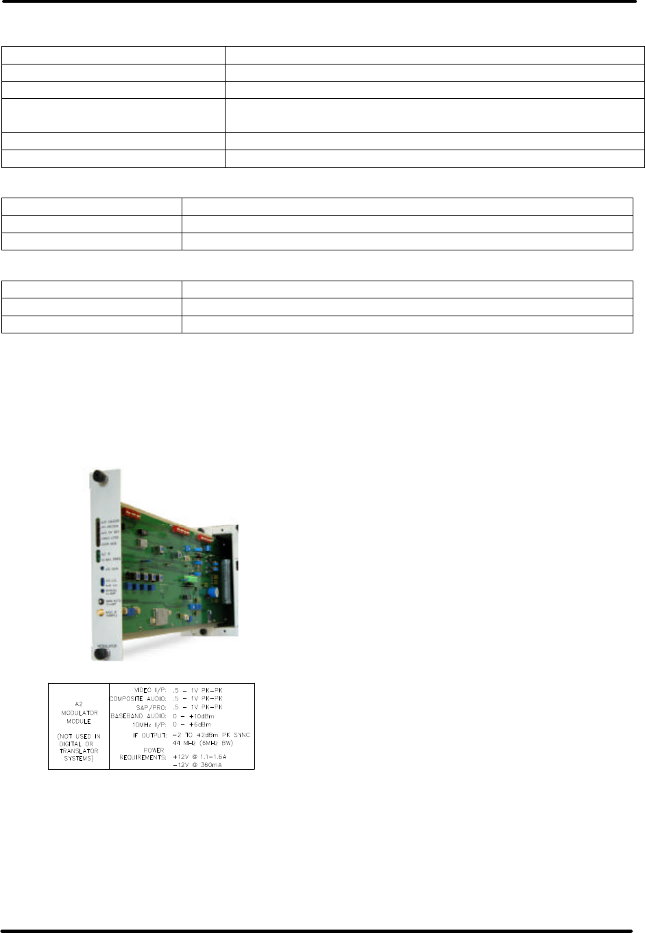
2.1.2 (A2) Modulator Module
Assembly (1301929; Appendix B)
NOTE: The Modulator module may not
be present in a translator system or in a
digital system.
NOTE: If both the Modulator and
Receiver are present in your system the
Modulated IF output from the Modulator
or Receiver must be selected. This is
accomplished by connecting a low or
removing the low to TB31-Pin 3 located
on the rear of the exciter/driver
assembly. By connecting the low, the
Modulator IF output is used by the IF
Processor module. By removing the low,
the IF from the internal or external
Receiver is used. (NOTE: The IF
Processor board must be configured for
external switching by placing jumper
W11 on J29 between pins 1 & 2).
The (A2) Modulator Assembly contains
the Modulator Board (1301797). The
modulator is broadcast quality and
provides front panel access to control and
monitoring points. The video level is
controlled through a sync tip clamp and
sync and white clipping circuitry. The IF
oscillator is oven controlled and locked to
a 10 MHz reference for stability. The IF
signal is fed through a SAW filter for
precise sideband shaping. The Modulator
operates using the baseband audio and
video inputs to produce a diplexed,
modulated, and on-channel frequency
visual + aural RF output that is cabled to
the IF Processing Module.
UHF Analog Driver/Transmitter/ Chapter 2, System Description,
Translator Maintenance & Remote Control Connections
LX Series, Rev. 3 2-6
Table 2-6. Modulator Front Panel Switch
SWITCH FUNCTION
MAN/AUTO CLAMP
SW1
When Manual Clamp is selected, the video level is set by the
Manual Bias Pot R67 located on the board. (NOTE: The pot is
factory set and needs no adjustment by the customer).
When Auto Clamp is selected, the video level control circuit
will automatically increase or decrease the video to maintain
the desired video level.
Table 2-7. Modulator Front Panel Status Indicators
LED FUNCTION
AUR UNLOCK
DS5 (Red) When lit it indicates that the 4.5 MHz VCO and the 10 MHz reference
are not PLL locked.
VIS UNLOCK
DS6 (Red) When lit it indicates that the 45.75 MHz VCXO and the 10 MHz
reference signal are not PLL locked.
AUD OV DEV
DS4 (Red) When lit it indicates the deviation level is more than ±80kHz
VIDEO LOSS
DS1 (Red) When lit it indicates the Video Input to the transmitter is lost.
OVER MOD
DS3 (Red) When lit it indicates the Video input level is too high.
ALT IF
DS7 (Green) When lit it indicates that external or alternate 4.5MHZ is present.
10 MHz PRES
DS2 (Green) When lit it indicates that a 10MHz reference is present to the
transmitter.
Table 2-8. Modulator Front Panel Control Adjustments
POTENTIOMETERS
DESCRIPTION
Video Gain (R42) Adjusts the level of the output video.
Visual Level (R214) Adjusts the Visual IF level that combines with the Aural IF.
Aural Level (R243) Adjusts the Aural IF level that combines with the Visual IF.
MONO (R110) Adjusts the deviation level of the balanced audio input.
STEREO (R132) Adjusts the deviation level of the composite audio input.
SAP/PRO (R150) Adjusts the deviation level of the subcarrier audio input.
Table 2-9. Modulator Front Panel Sample
SMA CONNECTOR DESCRIPTION
MOD IF SAMPLE (J10) Sample of the combined Aural IF and Visual IF signals.
UHF Analog Driver/Transmitter/ Chapter 2, System Description,
Translator Maintenance & Remote Control Connections
LX Series, Rev. 3 2-7
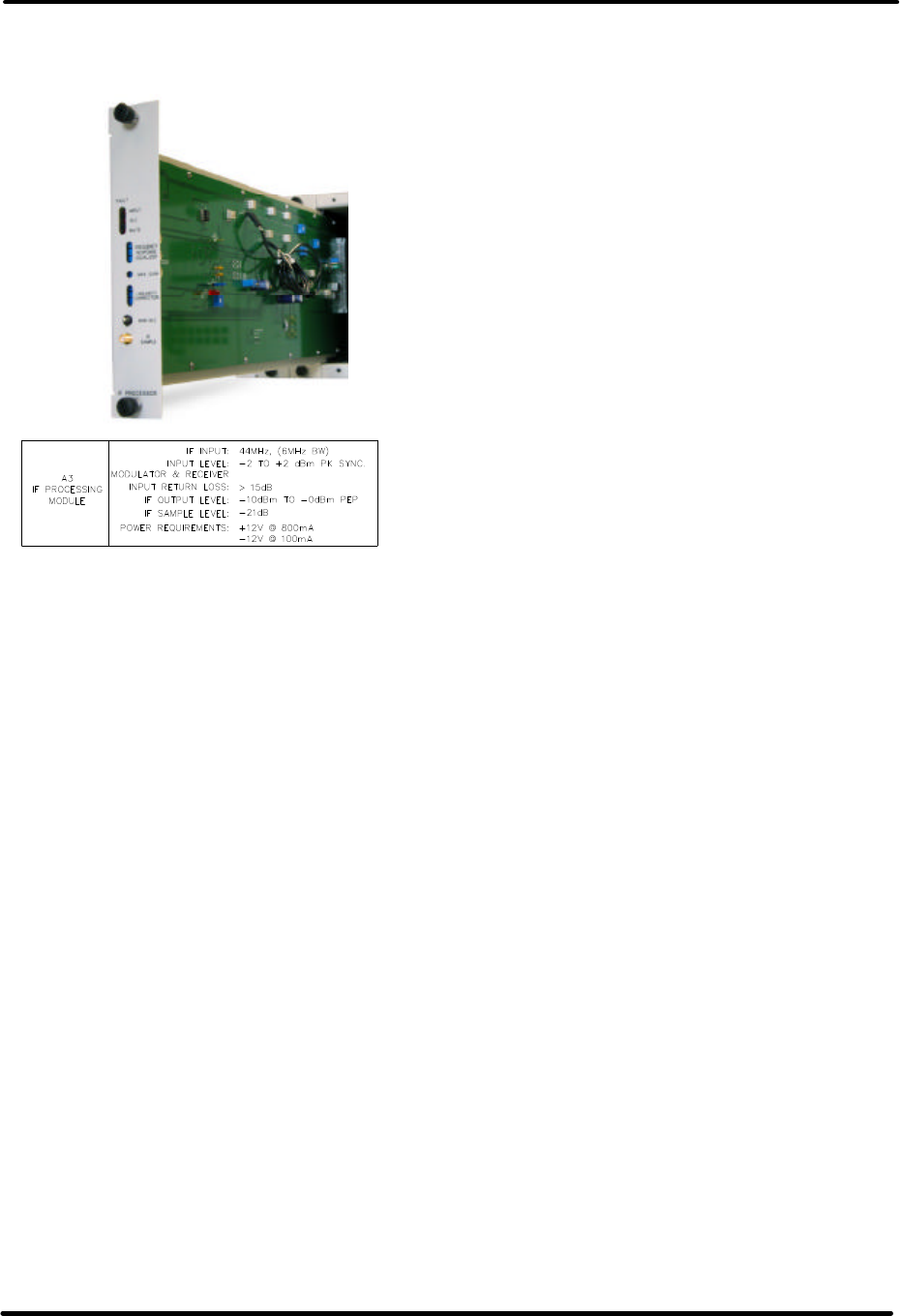
2.1.3 (A3) IF Processor Module
Assembly (1301938; Appendix B)
The (A3) IF Processor Assembly contains
the IF Processor Board (1301977). The IF
Processor provides pre-correction to
ensure broadcast quality output signal.
The pre-correction consists of amplitude
linearity correction, Incidental Carrier
Phase Modulation (ICPM) correction and
frequency response correction.
The IF Processor module is configured
either for an analog or digital system.
Pin 13C of the IF Processor module is
grounded in analog systems and left not
connected in digital systems. An IF
Processor Interlock signal is used to
report the presence of the IF Processor
module to the Control Monitoring board.
If the IF Processor interlock signal is not
present, the LX Series
Transmitter/Exciter Driver RF output is
Muted (turned off). If an analog IF
Processor module is installed and the
Modulation Present signal is not true,
the LX Series Transmitter/Exciter Driver
output is Muted (turned off).
The Control & Monitoring/Power Supply
module uses the IF Processor module for
System output power control. Through
the front panel display or a remote
interface, an operator can set the RF
output power level of the transmitter.
The range of RF power adjustment is
between 0% (full off) and 105% (full
power plus). A front panel IF Processor
module potentiometer sets the upper
limit of RF power at 120%. The
system's Control Monitoring board
compares the RF Power Monitoring
module RF power level with the desired
level and uses the IF Power Control PWM
line to correct for errors.
In digital systems, a digital level control
(DLC) voltage is generated on the IF
Processor module and sent to an
external digital modulator (DT1B/C). RF
power control is implemented by
changing the DLC voltage provided to
the external digital modulator. The 'RF
High' potentiometer sets the upper
adjusted range of RF control circuit
output to 120%.
The IF Processor module provides a
reference ALC voltage to the system's
Upconverter. When the ALC voltage
decreases, the Upconverter
automatically lowers the system output
power through the AGC circuits.
The IF Processor module has a front
panel switch to select Auto or Manual
ALC. When Manual ALC is selected, the
reference ALC voltage is set by a front
panel potentiometer. In this condition,
the RF power level control circuit is
removed from use. When the ALC select
switch is changed to Auto, the RF power
level control circuit will start at low
power and increase the RF output until
the desired output power is attained.
The IF Processor module Modulation
Present signal is monitored. If the
modulation level is too low or non-
existent, a Modulation Present Fault is
reported to the Control Monitoring
board. When the controller detects this
fault, it can be set to Automatically Mute
the transmitter or in Manual mode the
UHF Analog Driver/Transmitter/ Chapter 2, System Description,
Translator Maintenance & Remote Control Connections
LX Series, Rev. 3 2-8
transmitter will continue to operate at
25% output.
The IF Processor module Input Signal
level is monitored. If the signal level is
too low or non-existent, an Input Fault
is reported on the Control Monitoring
board. When the IF Processor board
detects an Input Signal Fault it
automatically Mutes the transmitter.
The system controller does not Mute on
an IF Processor Input Fault.
Table 2-10. IF Processor Front Panel Switch
SWITCH FUNCTION
MAN/AUTO ALC
When Manual ALC is selected, the reference ALC voltage is set
by the ALC Gain front panel potentiometer.
When Auto ALC is selected, the IF level control circuit will
automatically increase the IF output until the desired output
power is attained.
Table 2-11. IF Processor Front Panel Status Indicators
LED FUNCTION
INPUT FAULT (Red) When lit it indicates that there is a loss of the IF Input signal to the
IF Processor. Transmitter can be set to Mute on an IF Input Fault.
ALC Fault (Red) When lit it indicates that the required gain to produce the desired
output power level has exceeded the operational range of the ALC
circuit. The LED will also be lit when ALC is in Manual.
MUTE (Red) When lit it indicates that the IF input signal is cut back but the
enable to the Power Supply is present and the +32 VDC remains on.
Table 2-12. IF Processor Front Panel Control Adjustments
POTENTIOMETERS
DESCRIPTION
FREQUENCY
RESPONSE
EQUALIZER
These three variable resistors, R103, R106 & R274, adjust the
depth of gain for the three stages of frequency response correction.
ALC GAIN Adjusts the gain of the transmitter when the transmitter is in the
Auto ALC position.
MAN GAIN Adjusts the gain of the transmitter when the transmitter is in the
Manual ALC position.
LINEARITY
CORRECTION
These three variable resistors adjust the threshold cut in for the
three stages of linearity pre-correction. R211 and R216, the top
two pots, are adjusted to correct for in phase amplitude distortions.
R 231, the bottom pot, is adjusted to correct for quadrature phase
distortions.
Table 2-13. IF Processor Front Panel Sample
SMA CONNECTOR DESCRIPTION
IF SAMPLE Sample of the pre-corrected IF output of the IF Processor
UHF Analog Driver/Transmitter/ Chapter 2, System Description,
Translator Maintenance & Remote Control Connections
LX Series, Rev. 3 2-9
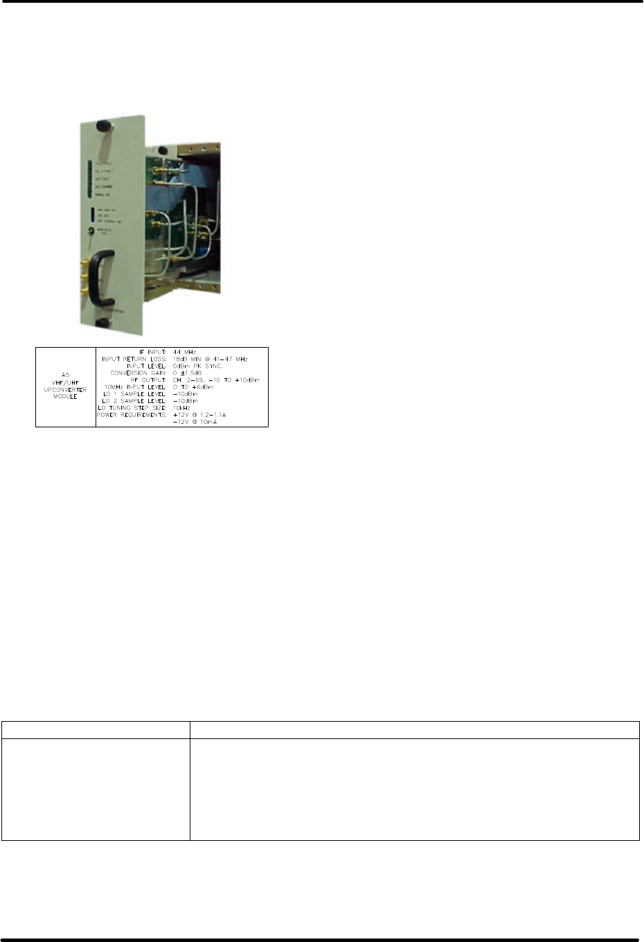
2.1.4 (A5) VHF/UHF Upconverter
Module Assembly (1303829;
Appendix B)
The VHF/UHF Upconverter Module
Assembly contains (A1) a Downconverter
Board Assembly (1303834), (A3) a First
Conversion Board, LX Series (1303838),
(A2) a L-Band PLL Board, LX Series
(1303846) and (A4) an Upconverter
Control Board (1304760).
A 0 dBm 44 MHz IF input to the
upconverter through the backplane
board is applied to a mixer mounted on
the first conversion board. Also applied
to the mixer is a nominal 1 GHz LO1.
The mixer converts it to a nominal
frequency centered at 1044 MHz. A
filter selects the appropriate conversion
product, which is then amplified to a
level of approximately –4 dBm. The
frequency of the first conversion LO1
can be shifted by ± 10 kHz to generate
channel offsets of 10kHz. For +offsets
the frequency is 999.99 MHz and for –
offsets the frequency is 1000.01 MHz.
This signal is applied to a second mixer
mounted on the downconverter board
that converts it back to a broadcast
channel (2-69) by an LO2 that operates
in 100kHz steps between 1.1-1.9 GHz
depending on the channel selected. The
LO2 frequency equals the Channel
center frequency plus the LO1 frequency
plus 44 MHz. (As an example CH14+:
Center Frequency is 473.01 MHz and
LO1 is 999.99 MHz therefore LO2 is
473.01 + 999.99 + 44, which equals
1517.00 MHz.)
The output of the mixer is applied to a
900 MHz Low pass filter to remove
unwanted conversion products. The
resulting signal is amplified and applied
to a Pin diode attenuator before it is
connected to the output of the
upconverter. This pin diode attenuator
adjusts the gain of the module and is
controlled by an Automatic Gain Control
circuit, which maintains a constant
power out of the upconverter, and also
the transmitter, that connects to the
power amplifier module.
Table 2-14. VHF/UHF Upconverter Front Panel Switch
SWITCH FUNCTION
MAN/AUTO AGC
(Left Manual, Right AGC)
When Manual AGC is selected, the reference AGC voltage is
set by the AGC Manual Gain front panel potentiometer.
When Auto AGC is selected, the RF power level control circuit
will automatically increase the RF output until the desired
output power is attained.
UHF Analog Driver/Transmitter/ Chapter 2, System Description,
Translator Maintenance & Remote Control Connections
LX Series, Rev. 3 2-10
Table 2-15. VHF/UHF Upconverter Front Panel Status Indicators
LED FUNCTION
PLL 1 Fault
(Red) When lit it indicates that the 1 GHz PLL is unlocked
PLL 2 Fault
(Red) When lit it indicates that the 1.1 –1.9 GHz PLL is unlocked
AGC Fault
(Red) When lit it indicates that the AGC is out of range.
AGC Override
(Red) When lit it indicates that the AGC is cutting back due to too much
drive to the driver module.
Man Gain
(Amber) When lit it indicates that the AGC is bypassed in Manual.
Table 2-16. VHF/UHF Upconverter Front Panel Control Adjustments
POTENTIOMETERS
DESCRIPTION
MAN GAIN ADJ Adjusts the gain of the upconverter and transmitter when in the
Manual AGC position.
AGC ADJ Adjusts the gain of the upconverter and transmitter when in the
Auto AGC position.
AGC CUTBACK ADJ
(AGC OVERRIDE) Adjusts the point at which the transmitter will cut back in power,
due to too much drive, when the Transmitter is in Auto AGC.
Table 2-17. VHF/UHF Upconverter Front Panel Samples
SMA CONNECTOR DESCRIPTION
LO1 SAMPLE Sample of the 1 GHz nominal LO1 signal in the Upconverter as
generated on the L-Band PLL Board.
LO2 SAMPLE Sample of the 1.1-1.9 GHz LO2 signal in the Upconverter as
generated on the First Conversion Board.
RF SAMPLE Sample of the On Channel RF Output of the Upconverter
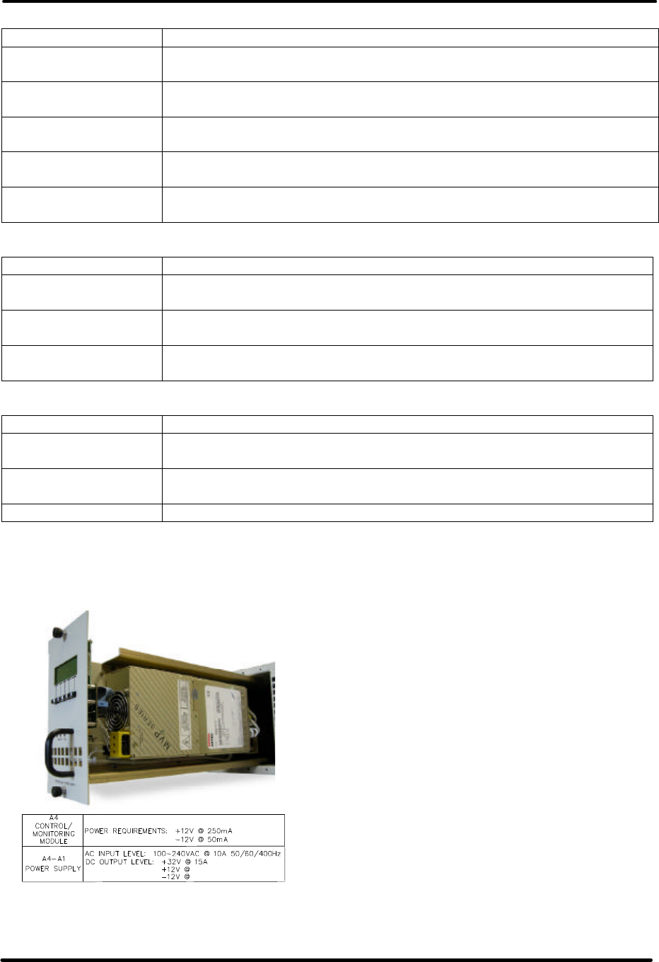
2.1.5 (A4) Control/Power Supply
Module Assembly (110 VAC,
1301936 or 220 VAC, 1303229;
Appendix B)
8 A
4 A
The (A4) Control & Monitoring/Power
Supply Assembly is configured at the
factory for operation at 110 VAC or 220
VAC. The assembly made up of a Control
Board (1302021), a Power Protection
Board (1302837) and a Switch Board
(1527-1406). The Assembly also
contains a switching power supply that
provides ±12 VDC to the rest of the
modules in the chassis and +32 VDC to
the Power Amplifier module.
The Assembly provides all transmitter
control and monitoring functions. The
Front panel LCD allows monitoring of
system parameters, including forward
and reflected power, transistor currents,
module temperatures and power supply
voltages. The LCD screens are detailed
in Chapter 3.
UHF Analog Driver/Transmitter/ Chapter 2, System Description,
Translator Maintenance & Remote Control Connections
LX Series, Rev. 3 2-11
Table 2-18. Controller/Power Supply Display
DISPLAY FUNCTION
LCD A 4 x 20 display providing a four-line readout of the internal
functions, external inputs, and status. See Chapter 3,
Controller/Power Supply Display Screens, for a listing of displays.
Table 2-19. Controller/Power Supply Status Indicator
LED FUNCTION
OPERATE
(green)
When lit it indicates that the transmitter is in the Operate Mode. If
transmitter is Muted the Operate LED will stay lit, the transmitter
will remain in Operate, until the input signal is returned.
FAULT
(red or green)
Red indicates that a problem has occurred in the transmitter. The
transmitter will be Muted or placed in Standby until the problem is
corrected.
DC OK
( red or green ) Green indicates that the switchable fuse protected DC outputs that
connect to the modules in the transmitter are OK.
Table 2-20. Controller/Power Supply Control Adjustments
POTENTIOMETERS
DESCRIPTION
DISPLAY CONTRAST Adjusts the contrast of the display for desired viewing of screen.
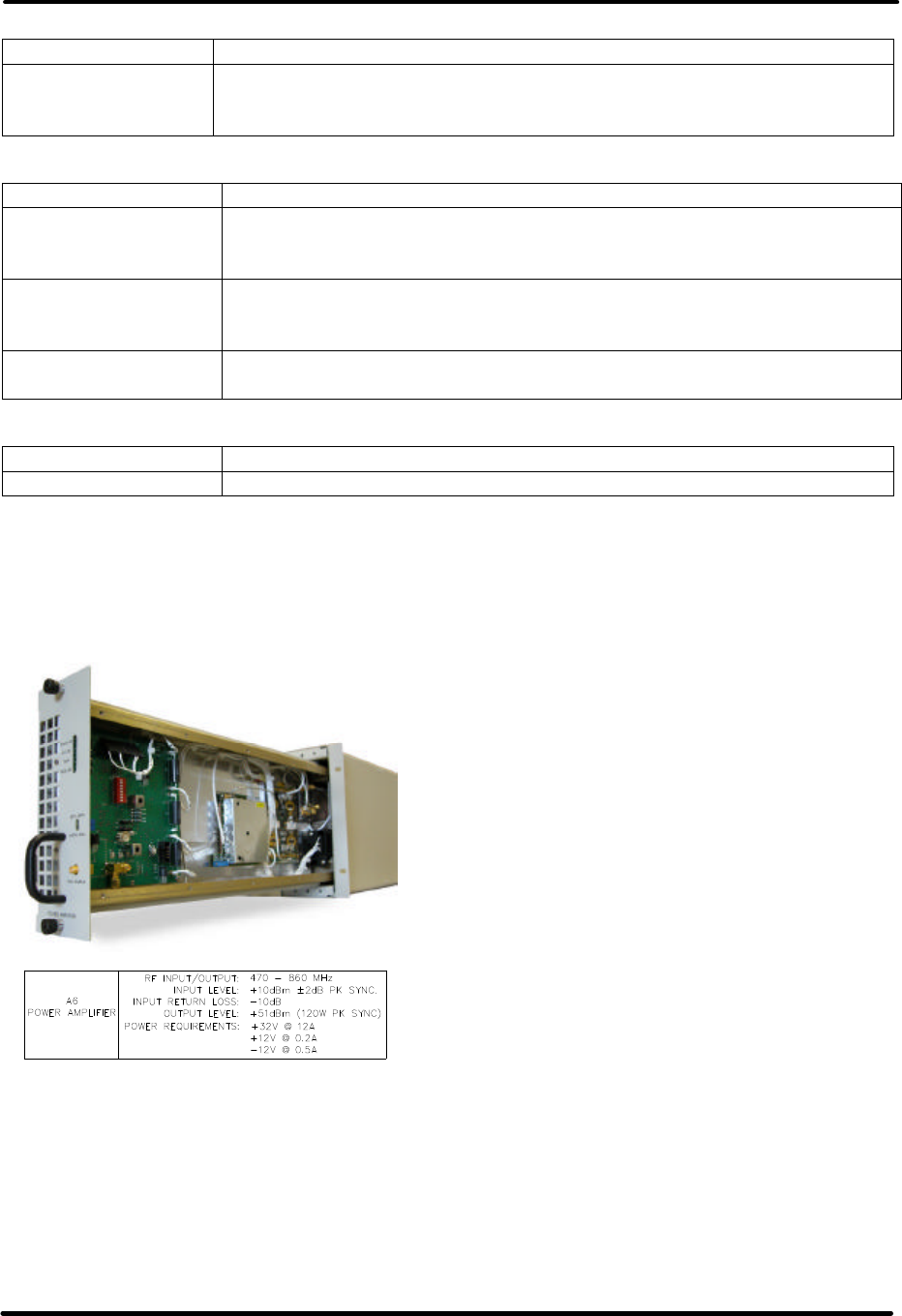
2.1.6 (A6) Exciter Power Amplifier
Module in (10-100W System or
driver in systems3kW & 4kW
1303770 OR in a 1 Watt Systems
1307184 OR in a 20W VHF LB
System 1307156; Appendix B)
NOTE: The (A6) Power Amplifier Module
Assembly (1303770) is used in the 10-
100 Watt Transmitter or as a driver in
3kW & 4KkW systems. The (1307184)
Power Amplifier Module Assembly is used
in 1 Watt Systems. The (1307156)
Power Amplifier Module Assembly is used
in 20 Watt VHF Low Band Systems.
The (A6) Power Amplifier Module
Assembly is made up of a Coupler Board
Assembly (1301949, 1141-1002, or
1007-1208), an Amplifier Control Board
(1303682 or 1301962), a 1 Watt Module
Assembly (1302891), a 40W UHF Module
(1304490 or 1206693) and a RF Module
Pallet, Philips (1300116).
The Power Amplifier Module contains
Broadband LDMOS amplifiers that cover
the entire UHF band with no tuning
required. They amplify the RF to the 1 to
100W output power level of the
transmitter or the drive level needed to
achieve the output power from the
external PA assemblies.
The Power Amplifier of the
Transmitter/Exciter Driver is used to
amplify the RF output of the
Upconverter module. A cable, located on
the rear chassis, connects the RF output
from the Upconverter at J23 to J24 the
RF input to the PA Assembly. This
module contains RF monitoring circuitry
for both an analog and a digital system.
Control and monitoring lines to the
Power Amplifier module are routed
through the floating blind-mate
connector of the Control &
Monitoring/Power Supply module.

UHF Analog Driver/Transmitter/ Chapter 2, System Description,
Translator Maintenance & Remote Control Connections
LX Series, Rev. 3 2-12
The Transmitter/Exciter Driver Power
Amplifier module and any External
Amplifier modules contain the same
control and monitoring board. This
board monitors RF output power, RF
reflected power, the current draw of
amplifier sections, the supply voltage,
and the temperature of the PA heat sink.
The RF power detector circuit outputs
vary with operating frequency. These
circuits must be calibrated at their
intended operating frequency. Front
panel adjustment potentiometers are
used to calibrate the following:
Power Amplifier Calibration Adjustments
in Analog Systems
R201 Reflected Power Cal
R202 Visual/Forward Power Cal
R203 Aural Power Cal
R204 Visual Offset Zero
R205 Aural Null
In analog systems, the Aural power of
an Exciter Driver Power Amplifier and
the Aural power of any external
amplifier will not be reported by the
system Control Monitoring module.
Additionally the Visual power of these
amplifiers, is reported as Forward Power
just like in digital systems. In analog
systems, aural and visual power will only
be reported for the final system RF
output.
If the Control Monitoring module is
monitoring a 1-100 Watt analog
Transmitter, system power is measured
in the Power Amplifier module. The
wired connections are transferred
through the power supply connector to
the backplane board on a five position
header. All four positions of control
board switch SW1 must be set on to
route these lines as the system's RF
power signals. In systems of output
power greater than 100 Watts analog,
system power is monitored by an
external module that is connected to
TB31 and control board SW1 switches
must be set off.
The Forward Power of the
Transmitter/Exciter Driver Power
Amplifier module is routed to the
Upconverter module as AGC #1. A
system over-drive condition is detected
when this value rises above 0.9 VDC.
When an over-drive condition is
detected, the Upconverter module
reduces its RF output level. For values
less than 0.9 VDC, the Upconverter uses
this voltage for automatic gain.
Table 2-21. Power Amplifier Status Indicator
LED FUNCTION
ENABLED
(Green)
When lit Green, it indicates that the PA is in the Operate Mode. If a
Mute occurs, the PA will remain Enabled, until the input signal is
returned.
DC OK
(Green) When lit Green, it indicates that the fuse protected DC inputs to the
PA module are OK.
TEMP
(Green) When lit Green, it indicates that the temperature of the heatsink
assembly in the module is below 78°C.
MOD OK
(Green) When lit Green, it indicates that the PA Module is operating and has
no faults.
MOD OK
(Red)
If the Module OK LED is Red and blinking a fault is present.
1 Blink indicates Amplifier Current Fault.
2 Blinks indicate Temperature Fault.
3 Blinks indicate +32V Power Supply Over Voltage Fault.
4 Blinks indicate +32V Power Supply Under Voltage Fault.
5 Blinks indicate Reflected Power Fault.
6 Blinks indicate +12V or –12V Power Supply Fault.
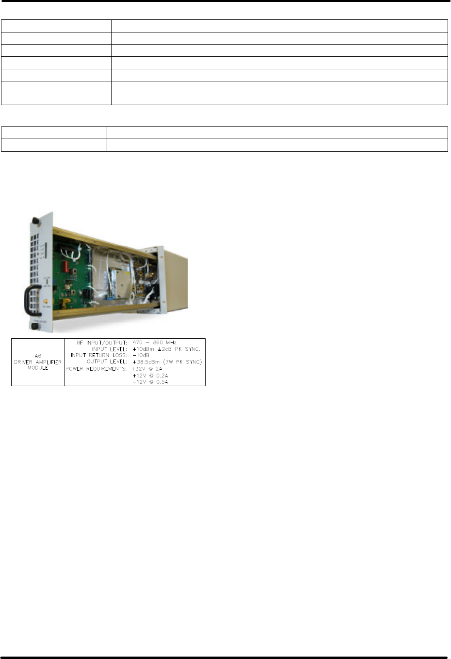
UHF Analog Driver/Transmitter/ Chapter 2, System Description,
Translator Maintenance & Remote Control Connections
LX Series, Rev. 3 2-13
Table 2-22. Power Amplifier Control Adjustments
POTENTIOMETERS
DESCRIPTION
RFL CAL Adjusts the gain of the Reflected Power monitoring circuit
VISUAL CAL Adjusts the gain of the Visual / Forward Power monitoring circuit
AURAL CAL Adjusts the gain of the Aural Power monitoring circuit
VISUAL ZERO Adjusts the offset of the Forward Power monitoring circuit
AURAL NULL Adjusts the offset of the Forward Power monitoring circuit based on
the Aural signal level.
Table 2-23. Power Amplifier Sample
DISPLAY FUNCTION
FWD SAMPLE RF sample of the amplified signal being sent out the module on J25.
2.1.6.1 (A6) Driver Amplifier Module
Assembly {1303771(1kW),
1303874(2kW) or 1307761 (5kW &
6kW); Appendix B}
NOTE: The (A6) Driver Amplifier Module
Assembly {1303771(1kW),
1303874(2kW), or 1307761(5kW &
6kW)} replaces the Power Amplifier
Module Assembly (1303770) when the
amplifier module is used as a driver for
any external PA assemblies.
The (A6) Power Amplifier Module
Assembly is made up of a Coupler Board
Assembly (1227-1316) or a Coupler
Board (1301949) in a 1307761 PA
Module, an Amplifier Control Board
(1303682), a 1 Watt Module Assembly
(1302891), a 40W UHF Module
(1304490) and in 1303874 & 1307761
Assemblies there is also a RF Module
Pallet (1300116).
The Driver Power Amplifier Module
contains Broadband LDMOS amplifiers
that cover the entire UHF band with no
tuning required. They amplify the RF to
the power level, 7 Watts Peak of Sync is
maximum, that is needed to drive the
external amplifiers to the output power
level of the transmitter. The Driver
Power Amplifier is used to amplify the
RF output of the Upconverter module. A
cable, located on the rear chassis,
connects the RF output from the
LO/Upconverter at J23 to J24 the RF
input to the driver PA Assembly. This
module contains RF monitoring circuitry
for both an analog and a digital system.
Control and monitoring lines to the
Driver Power Amplifier module are
routed through the floating blind-mate
connector of the Control &
Monitoring/Power Supply module.
The Driver Power Amplifier module and
any External Amplifier modules contain
the same control and monitoring board.
This board monitors RF output power,
RF reflected power, the current draw of
amplifier sections, the supply voltage,
and the temperature of the PA heat sink.
The RF power detector circuit outputs
vary with operating frequency. These
circuits must be calibrated at their
intended operating frequency. Front
panel adjustment potentiometers are
used to calibrate the following:
Power Amplifier Calibration Adjustments
in Analog Systems
R201 Reflected Power Cal
R202 Visual/Forward Power Cal
R203 Aural Power Cal

UHF Analog Driver/Transmitter/ Chapter 2, System Description,
Translator Maintenance & Remote Control Connections
LX Series, Rev. 3 2-14
R204 Visual Offset Zero
R205 Aural Null
In analog systems, the Aural power of
an Exciter Driver Power Amplifier and
the Aural power of any external PA
amplifiers will not be reported by the
system Control Monitoring module.
Additionally the Visual power of these
amplifiers, is reported as Forward Power
just like in digital systems. In analog
systems, aural and visual power will only
be reported for the final system RF
output.
In digital systems, the Forward power of
an Exciter Driver Power Amplifier and
the Forward power of any external
amplifiers, are reported by the system
Control Monitoring module.
If the Control Monitoring module is
monitoring a 10-100 Watt Transmitter,
system power is measured in the Power
Amplifier module. The wired
connections are transferred through the
power supply connector to the
backplane board on a five position
header. All four positions of control
board switch SW1 must be set on to
route these lines as the system's RF
power signals. In systems of output
power greater than 100 Watts, system
power is monitored by an external
module that is connected to TB31. In
this configuration switches SW1 on the
control board must be set off.
The Forward Power of the Exciter Driver
Power Amplifier module is routed to the
Upconverter module as AGC #1. A
system over-drive condition is detected
when this value rises above 0.9 VDC.
When an over-drive condition is
detected, the Upconverter module
reduces its RF output level.
For values less than 0.9 VDC, the
Upconverter uses this voltage for
automatic gain.
Table 2-24. Driver Amplifier Status Indicator
LED FUNCTION
ENABLED
(Green)
When lit Green, it indicates that the PA is in the Operate Mode. If a
Mute occurs, the PA will remain Enabled, until the input signal is
returned.
DC OK
(Green) When lit Green, it indicates that the fuse protected DC inputs to the
PA module are OK.
TEMP
(Green) When lit Green, it indicates that the temperature of the heatsink
assembly in the module is below 78°C.
MOD OK
(Green) When lit Green, it indicates that the PA Module is operating and has
no faults.
MOD OK
(Red)
If the Module OK LED is Red and blinking a fault is present.
1 Blink indicates Amplifier Current Fault.
2 Blinks indicate Temperature Fault.
3 Blinks indicate +32V Power Supply Over Voltage Fault.
4 Blinks indicate +32V Power Supply Under Voltage Fault.
5 Blinks indicate Reflected Power Fault.
6 Blinks indicate +12V or –12V Power Supply Fault.
Table 2-25. Driver Amplifier Control Adjustments
POTENTIOMETERS
DESCRIPTION
RFL CAL Adjusts the gain of the Reflected Power monitoring circuit
VISUAL CAL Adjusts the gain of the Visual / Forward Power monitoring circuit
AURAL CAL Adjusts the gain of the Aural Power monitoring circuit
VISUAL ZERO Adjusts the offset of the Forward Power monitoring circuit
AURAL NULL Adjusts the offset of the Forward Power monitoring circuit based on
the Aural signal level.

UHF Analog Driver/Transmitter/ Chapter 2, System Description,
Translator Maintenance & Remote Control Connections
LX Series, Rev. 3 2-15
Table 2-26. Driver Amplifier Sample
DISPLAY FUNCTION
FWD SAMPLE RF sample of the amplified signal being sent out the module on J25.
2.1.7 RF Output Assemblies
The RF output from the exciter power
amplifier is at the RF output jack, an “N”
connector J25, PA RF Output, of the
chassis assembly. If the exciter
assembly is used as a driver, the output
connects to the input of the PA Assembly
mounted beneath the exciter assembly.
If the exciter assembly is used as a 10W
to 100W transmitter, then the output
connects directly to the bandpass filter
for the system.
The RF output of the transmitter is
typically connected to a bandpass filter
and then to a trap filter mounted on the
rear of the assembly. The bandpass and
trap filters are tuned to eliminate
unwanted sideband and harmonic
frequencies. Located on the output of
the trap filter is a BNC output sample
jack that can be used for test purposes.
2.2 Control and Status
The control and status readings of the
exciter/amplifier Chassis assembly are
found by operating the front panel
display screen on the front of the
assembly. Detailed information on the
use of the screens is found in chapter 3.
2.2.1 Front Panel Display Screens
A 4 x 20 display located on the front of
the Control & Monitoring/Power Supply
Module is used in the LX Series
transmitter for control of the operation
and display of the operating parameters
of the transmitter. Refer to Chapter 3
for descriptions of the screens.
2.3 System Operation
When the transmitter is in operate, as set
by the menu screen located on the
Control & Monitoring Module, the
following occurs. The IF Processor will be
enabled and the mute indicator on the
front panel will be extinguished. The
+32 VDC stage of the Power Supply in
the Control & Monitoring Module is
enabled, the operate indicator on the
front panel is lit and the DC OK on the
front panel should also be green. The
enable and DC OK indicators on the PA
Module will also be green.
When the transmitter is in standby. The
IF Processor will be disabled, the mute
indicator on the front panel will be red.
The +32 VDC stage of the Power Supply
in the Control & Monitoring Module is
disabled, the operate indicator on the
front panel will be extinguished and the
DC OK on the front panel should remain
green. The enable indicator on the PA
Module is also extinguished.
If the transmitter does not switch to
Operate when the operate menu is
switched to Operate, check that all faults
are cleared and that the remote control
terminal block stand-by signal is not
active.
The transmitter can be controlled by the
presence of a modulated input signal. If
the input signal to the transmitter is lost,
the transmitter will automatically cutback
and the input fault indicator on the IF
Processor module will light. When the
video input signal returns, the
transmitter will automatically return to
full power and the input fault indicator
will be extinguished.
2.3.1 Principles of Operation
Operating Modes
This transmitter is either operating or in
standby mode. The sections below
discuss the characteristics of each of
these modes.

UHF Analog Driver/Transmitter/ Chapter 2, System Description,
Translator Maintenance & Remote Control Connections
LX Series, Rev. 3 2-16
Operate Mode
Operate mode is the normal mode for
the transmitter when it is providing RF
power output. To provide RF power to
the output, the transmitter will not be in
mute. Mute is a special case of the
operate mode where the +32 VDC
section of the power supply is enabled
but there is no RF output power from
the transmitter. This condition is the
result of a fault that causes the firmware
to hold the IF Processor module in a
mute state.
Operate Mode with Mute Condition
The transmitter will remain in the
operate mode but will be placed in mute
when the following fault conditions
exists in the transmitter.
• Upconverter is unlocked
• Upconverter module is not present
• IF Processor module is not present
• Modulator (if present) is in
Aural/Visual Mute
Entering Operate Mode
Entering the operate mode can be
initiated a few different ways by the
transmitter control board. A list of the
actions that cause the operate mode to
be entered is given below:
• A low on the Remote Transmitter
Operate line.
• User selects "OPR" using switches
and menus of the front panel.
• Receipt of an “Operate CMD” over
the serial interface.
There are several fault or interlock
conditions that may exist in the
transmitter that will prevent the
transmitter from entering the operate
mode. These conditions are:
• Power Amplifier heat sink
temperature greater than 78°C.
• Transmitter is Muted due to
conditions listed above.
• Power Amplifier Interlock is high
indicating that the amplifier is not
installed.
Standby Mode
The standby mode in the transmitter
indicates that the output amplifier of the
transmitter is disabled.
Entering Standby Mode
Similar to the operate mode, the
standby mode is entered using various
means. These are:
• A low on the Remote Transmitter
Stand-By line.
• Depressing the “STB” key on
selected front panel menus.
• Receipt of a “Standby CMD” over the
serial interface.
Auto Standby Mode
The FCC requires that certain
transmitters automatically switch to
standby operation on loss of video input.
The LX Series transmitter incorporates
this feature as a user configurable
setting. When Auto Stand-By on
modulation loss is selected in the set-up
menus, the transmitter temporarily
switches to standby after ten seconds of
modulation loss. When the modulated
signal as reported by the IF Processor
module is again present, the transmitter
automatically returns to Operate mode.
This feature is implemented in
transmitter software versions 1.4 and
above.
RF System Interlock
A RF System Interlock signal is provided
through TB30-5. When this signal's
circuit is completed to ground such as
through a wire between TB30-5 and
TB30-15, the transmitter is allowed to

UHF Analog Driver/Transmitter/ Chapter 2, System Description,
Translator Maintenance & Remote Control Connections
LX Series, Rev. 3 2-17
operate. If this circuit is opened, the
transmitter switches to a Mute condition.
This circuit may be completed through
coax relay contacts and reject load
contact closures to assure the RF output
system is available to receive the
transmitter's output RF signal. This
feature is implemented in transmitter
software versions 1.4 and above.
Table 2-27: UHF Television Frequencies
CH
# CENTER
FREQUENCY
+ Offset - Offset CH
# CENTER
FREQUENCY
+ Offset
- Offset
14 473 MHz 473.01 472.99 42 641 MHz 641.01 640.99
15 479 MHz 479.01 478.99 43 647 MHz 647.01 646.99
16 485 MHz 485.01 484.99 44 653 MHz 653.01 652.99
17 491 MHz 491.01 490.99 45 659 MHz 659.01 658.99
18 497 MHz 497.01 496.99 46 665 MHz 665.01 664.99
19 503 MHz 503.01 502.99 47 671 MHz 671.01 670.99
20 509 MHz 509.01 508.99 48 677 MHz 677.01 676.99
21 515 MHz 515.01 514.99 49 683 MHz 683.01 682.99
22 521 MHz 521.01 520.99 50 689 MHz 689.01 688.99
23 527 MHz 527.01 526.99 51 695 MHz 695.01 694.99
24 533 MHz 533.01 532.99 52 701 MHz 701.01 700.99
25 539 MHz 539.01 538.99 53 707 MHz 707.01 706.99
26 545 MHz 545.01 544.99 54 713 MHz 713.01 712.99
27 551 MHz 551.01 550.99 55 719 MHz 719.01 718.99
28 557 MHz 557.01 556.99 56 725 MHz 725.01 724.99
29 563 MHz 563.01 562.99 57 731 MHz 731.01 730.99
30 569 MHz 569.01 568.99 58 737 MHz 737.01 736.99
31 575 MHz 575.01 574.99 59 743 MHz 743.01 742.99
32 581 MHz 581.01 580.99 60 749 MHz 749.01 748.99
33 587 MHz 587.01 586.99 61 755 MHz 755.01 754.99
34 593 MHz 593.01 592.99 62 761 MHz 761.01 760.99
35 599 MHz 599.01 598.99 63 767 MHz 767.01 766.99
36 605 MHz 605.01 604.99 64 773 MHz 773.01 772.99
37 611 MHz 611.01 610.99 65 779 MHz 779.01 778.99
38 617 MHz 617.01 616.99 66 785 MHz 785.01 784.99
39 623 MHz 623.01 622.99 67 791 MHz 791.01 790.99
40 629 MHz 629.01 628.99 68 797 MHz 797.01 796.99
41 635 MHz 635.01 634.99 69 803 MHz 803.01 802.99

UHF Analog Driver/Transmitter/ Chapter 2, System Description,
Translator Maintenance & Remote Control Connections
LX Series, Rev. 3 2-18
Operating Frequency
The LX Series transmitter/translator
controller is designed to operate on UHF
frequencies. Refer to Table 2-27 for the
typical UHF channel center and + & -
offset frequencies, which are used in
setting the LO1 and LO2 frequencies in
the Upconverter Module. The exact
output frequency of the transmitter can
be set to one of the standard UHF
frequencies, or to a custom frequency
using the software channel set-up menu
on the Controller Module. Since RF
performance of the transmitter requires
different hardware for different
frequency bands, not all frequency
configurations are valid for a specific
transmitter. The Power detectors in the
transmitter are frequency dependent,
therefore detectors of power amplifiers
are calibrated at their frequency of use.
The detectors for System RF monitoring
are also calibrated at the desired
frequency of use. Refer to Chapter 5 for
the Channel Change Procedure.
2.4 Maintenance
The Innovator LX Series Driver/
Transmitter/Translator is designed with
components that require little or no
periodic maintenance except for the
routine cleaning of the fans and the front
panels of the modules and the periodic
check of general tightness of hardware.
It is recommended that periodically, the
time interval depends on the amount of
movement the cabinet receives, all
mounting hardware, holding tray slides,
shelving and mounting plates inside the
cabinet are checked for tightness. All
screws and bolts that are accessible
should be tightened initially when the
transmitter is received and periodically
thereafter if the transmitter is moved by
vehicle. All coaxial connectors, hard-line
connections and hardware holding
combiners, splitters, or any other
mounted items should be checked and
tightened. Check the front panel
thumbscrews that hold the Exciter/Driver
Sleds, Amplifier Module and Power
Supply Sleds in place are tight. This is
especially important after the transmitter
has been transported.
The amount of time between cleanings
depends on the conditions within the
transmitter room. While the electronics
have been designed to function even if
covered with dust, a heavy buildup of
dust, dirt, or insects will affect the
cooling of the components. This could
lead to a thermal shutdown or the
premature failure of the affected module.
When the front panels of the modules
become dust covered, the module should
be pulled out and any accumulated
foreign material should be removed.
NOTE: To remove the driver/power
amplifier module, mounted in the
exciter/driver assembly, the input and
output cables must be removed from the
rear of the module and also a 6/32” x ½”
Philips screw, mounted between the two
connectors, needs to be removed before
the module will pull out. After removal of
the screw, which is used to hold the
module in place during shipping, it does
not need to be replaced.
NOTE: To remove the Combiner Module,
found in the power amplifier assembly in
high power transmitters, the output cable
must be removed from the rear of the
module and also two 8/32” x ½” Philips
screws, mounted above the connector,
need to be removed before the module
will pull out. After removal of the screws,
which are used to hold the module in
place during shipping, they do not need
to be replaced.
A vacuum cleaner, utilizing a small,
wand-type attachment, is an excellent
way to suction out the dirt. Alcohol and
other cleaning agents should not be used
unless you are certain that the solvents
will not damage components or the silk-
screened markings on the modules and
boards. Water-based cleaners can be
used, but do not saturate the
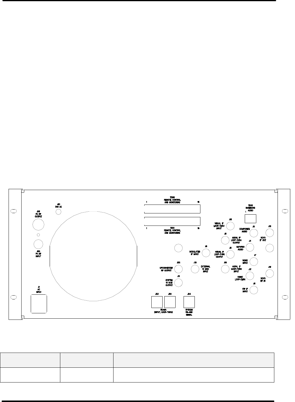
UHF Analog Driver/Transmitter/ Chapter 2, System Description,
Translator Maintenance & Remote Control Connections
LX Series, Rev. 3 2-19
components. The fans and heatsinks
should be cleaned of all dust or dirt to
permit the free flow of air for cooling
purposes.
It is recommended that the operating
parameters of the driver/transmitter be
recorded from the LEDs on the modules
and the LCD system metering on the
control/monitoring module at least once
a month. It is suggested that this data be
retained in a rugged folder or envelope.
2.5 Customer Remote Connections
The remote monitoring and operation of
the transmitter is provided through jacks
TB30 and TB31 located on the rear of the
chassis assembly. If remote connections
are made to the transmitter, they must
be made through plugs TB30 and TB31
at positions noted on the transmitter
interconnect drawing and Table 2-28.
TB30 and TB31 are 18 position terminal
blocks that are removable from their
sockets to make connections easier. Just
grasp and pull connector straight out.
After connections are made, replace the
connector and push firmly to seat the
connector in the socket.
If your system contains the Optional
Exciter Switcher Assembly, there are also
remote connections that can be made to
the Exciter Switcher Assembly. They
connect to TB1 on the rear of the exciter
switcher tray. Refer to Table 2-29 and to
the Exciter Switcher Board schematic
drawing (1305705) located in Appendix B
for the pin out and descriptions.
NOTE: If a Burk GSC 3000 Remote
Control Interface is used, refer to the
Interconnect Drawing (1307269), found
in the Appendix B of this Instruction
Manual, for the point to point
connections.
Figure 2-3. Exciter/Driver Chassis Assembly Rear View
Table 2-28: LX Series Chassis Assembly Hard Wired Remote Interface Connections to
TB30 or TB31, 18 pos. Terminal Blocks Located on the Rear of the Assembly
Signal Name Pin
Designations Signal Type/Description
RMT Transmitter
State TB30-1 Discrete Open Collector Output - A low indicates
that the transmitter is in the operate mode.
TB30
TB31

UHF Analog Driver/Transmitter/ Chapter 2, System Description,
Translator Maintenance & Remote Control Connections
LX Series, Rev. 3 2-20
Signal Name Pin
Designations Signal Type/Description
RMT Transmitter
Interlock TB30-2
Discrete Open Collector Output - A low indicated
the transmitter is OK or completes a interlock daisy
chain. When the transmitter is not faulted, the
interlock circuit is completed.
RMT Transmitter
Interlock Isolated
Return TB30-3
Ground - Configurable ground return which can be
either jumpered directly to ground or it can be the
“source” pin of an FET so that the transmitter
interlock can be daisy chained with other
transmitters. This signal does not directly interface
to the microcontroller.
RMT AUX IO 1 TB30-4
Discrete Open Collector Inputs, Discrete Open
Drain Outputs, or 0 - 5 VDC Analog Input - When
used as an output, this line is pulled to +5 VDC
with a 1.0 kO resistor for logic high and pulled to
ground for a low. A diode allows this line to be
pulled up to 12 VDC. When used as a digital input,
this line considers all values over 2 Volts as high
and those under 1 volt as low. As an analog input,
this line is protected by a 5.1 zener diode.
RMT RF System
Interlock TB30-5
When this signal's circuit is completed to ground
such as through a jumper between TB30-5 and
TB30-15, the transmitter is allowed to operate. If
this circuit is opened, the transmitter switches to a
Mute condition. Implemented in transmitter
software versions 1.4 and above.
RMT
Transmitter
Operate TB30-6 Discrete Open Collector Input - A pull down to
ground on this line indicates that the transmitter is
to be placed into the operate mode.
RMT
Transmitter
Stand-By TB30-7 Discrete Open Collector Input - A pull down to
ground on this line indicates that the transmitter is
to be placed into the standby mode.
RMT Power Raise TB30-8 Discrete Open Collector Input - A pull down to
ground on this line indicates that the transmitter
power is to be raised.
RMT Power Lower TB30-9 Discrete Open Collector Input - A pull down to
ground on this line indicates that the transmitter
power is to be lowered.
RMT
System Reflect
Power TB30-10
Analog Output (0 to 4.0 V). This is a buffered loop
through of the calibrated “System Reflected Power
” and indicates the transmitter's reflected output
power. The scale factor is 25% = 3.2V.
RMT System
Visual/Forward
Power TB30-11
Analog Output (0 to 4.0 V). This is a buffered loop
through of the calibrated “System Visual/Avg.
Power ”. Indicates the transmitter's Visual /
Average power. Scale factor is 100% = 3.2V.
RMT
System Aural
Power TB30-12
Analog Output (0 to 4.0 V). This is a buffered loop
through of the calibrated “System Aural Power ”.
Indicates the transmitter's forward Aural output
power. The scale factor is 100% = 3.2V.
RMT Spare 1 TB30-13 Remote connection to spare module - Use is TBD.
RMT Spare 2 TB30-14 Remote connection to spare module - Use is TBD.
UHF Analog Driver/Transmitter/ Chapter 2, System Description,
Translator Maintenance & Remote Control Connections
LX Series, Rev. 3 2-21
Signal Name Pin
Designations Signal Type/Description
System Reflect
Power TB31-13
Analog Input (0 to 1.00 V). This is the input of the
“System Reflected Power ” indicating the
transmitter's reflected output power. The scale
factor is 25% = 0.80V.
System Visual /
Forward Power TB31-14
Analog Input (0 to 1.00 V). This is the input of the
“System Visual / Forward Power ” indicating the
transmitter's forward Visual / Forward output
power. The scale factor is 100% = 0.80V.
System Aural
Power TB31-15
Analog Input (0 to 1.00 V). This is the input of the
“System Aural Power ” indicating the transmitter's
forward Aural output power. The scale factor is
100% = 0.80V.
IF Processor
IF Signal Select TB31-3
Discrete Open Collector Input – By connecting a
low to this pin, the Modulator IF source is used by
the IF Processor module. When floating the IF
from the internal or external Receiver is used.
(NOTE: The IF Processor board must be configured
for external switching by placing jumper W11 on
J29 between pins 1 & 2).
IF Processor
DLC Voltage TB31-4 Analog Output (0 to 5.00 V). This is the input of IF
Processor module for digital system RF output
power control.
UC AGC #2
Voltage TB31-5
Auxiliary Analog Input (0 to 1V). This voltage is
used by the Upconverter for gain control. Linear
signal with display resolution of 0.01 %. Primary
signal source is J34-1.
RMT Ground TB30-15, and
17 Ground pins available through Remote
RMT Ground TB31-1, 2, 6 to
12, and 17 Ground pins available through Remote
RMT +12 VDC TB30-16
TB31-16 +12 VDC available through Remote w/ 2 Amp re-
settable fuse
RMT -12 VDC TB30-18
TB31-18 -12 VDC available through Remote w/ 2 Amp re-
settable fuse
NOTE: If a Burk GSC 3000 Remote Control Interface is used, refer to the Interconnect
Drawing (1307269), found in the Appendix A of this Instruction Manual, for the point to
point connections.
Table 2-29: (Optional) Exciter Switcher Hard Wired Remote Interface Connections to TB1,
18 pos. Terminal Block are located on the Rear of the Exciter Switcher Tray Assembly.
Signal Name Pin
Designations Signal Type/Description
Select Automatic
Operation TB1-1 0 = SET, NC = No Change
Select Manual Operation TB1-2 0 = SET, NC = No Change
Select Exciter A (1) TB1-3 0 = SET, NC = No Change
Select Exciter B (2) TB1-4 0 = SET, NC = No Change

UHF Analog Driver/Transmitter/ Chapter 2, System Description,
Translator Maintenance & Remote Control Connections
LX Series, Rev. 3 2-22
Signal Name Pin
Designations Signal Type/Description
Selected Exciter to
Operate TB1-5 0 = SET, NC = No Change
Selected Exciter to
Standby TB1-6 0 = SET, NC = No Change
Fault Log Clear Exciter A
(1) TB1-7 0 = CLEAR, NC = No Change
Fault Log Clear Exciter A
(2) TB1-8 0 = CLEAR, NC = No Change
TB1-9 NOT USED IN THIS CONFIGURATION
TB1-10 NOT USED IN THIS CONFIGURATION
Ground TB1-11 Ground
Selected Operation TB1-12 0 = Auto, Open = Manual
Selected Exciter TB1-13 0 = A, Open = B
Selected Exciter Fault
Log Entries TB1-14 0 = None, Open = Log Has Entries
Selected Exciter Current
Error Status TB1-15 0 = None, Open = Has Errors
Alternate Exciter Fault
Log Entries TB1-16 0 = None, Open = Log Has Entries
Alternate Exciter
Current Error Status TB1-17 0 = None, Open = Has Errors
Ground TB1-18 Ground
NOTE: In versions previous to 2.0, for the automatic switching to the back up exciter,
the Error, Fault, Log in the back up exciter must be cleared of all Previous Faults..
UHF Analog Driver/Transmitter/ Chapter 3, Site Considerations,
Translator Installation and Setup Procedures
LX Series, Rev. 3 3-1
Chapter 3
Site Considerations, Installation and Setup Procedures
Table 3-1: LX Series Transmitters/Drivers AC Input and Current Requirements.
Transmitter/
Driver Voltage Current
10 Watt 117/220 VAC 5 Amps
100 Watt 117/220 VAC 10 Amps
250 Watt 220 VAC 10 Amps to the Exciter/Amplifier Cabinet
500 Watt 220 VAC 15 Amps to the Exciter/Amplifier Cabinet
1000 Watt 220 VAC 25 Amps to the Exciter/Amplifier Cabinet
2000 Watt 220 VAC 45 Amps to the Exciter/Amplifier Cabinet
3000 Watt 220 VAC 65 Amps to the Exciter/Amplifier Cabinet
220 VAC 45 Amps to the Exciter/Amplifier Cabinet
4000 Watt 220 VAC 40 Amps to the Amplifier Cabinet
220 VAC 45 Amps to the Exciter/Amplifier Cabinet
5000 Watt 220 VAC 60 Amps to the Amplifier Cabinet
220 VAC 65 Amp to the Exciter/Amplifier Cabinet
6000 Watt 220 VAC 60 Amps to the Amplifier Cabinet
3.1 Site Considerations
There are special considerations that need
to be taken into account before the
Innovator LX Series analog
driver/transmitter can be installed. For
example, if the installation is completed
during cool weather, a heat-related
problem may not surface for many
months, suddenly appearing during the
heat of summer. This section provides
planning information for the installation
and set up of the driver/transmitter.
The AC input and current requirements
for LX Series transmitters are shown in
Table 3-1.
NOTES: The transmitter is factory set
for either 110 VAC or 220 VAC
operation as directed by customer.
Transmitters 250 Watts or above use
220 VAC Input only.
Transmitters 4000 Watts and above
require two 220 VAC Inputs, one to
the exciter/driver and one to the
amplifier cabinet.
All currents are with a Black picture
Check that your site has the needed
power requirements.
The LX Series Analog Transmitters are
designed and built to provide long life
with a minimum of maintenance. The
environment in which they are placed is
important and certain precautions must
be taken. The three greatest dangers to
the transmitter are heat, dirt, and
moisture. Heat is usually the greatest
problem, followed by dirt, and then
moisture. Over-temperature can cause
heat-related problems such as thermal
runaway and component failure. Each
amplifier module in the transmitter
contains a thermal interlock protection
circuit that will shut down that module
until the temperature drops to an
acceptable level.
A suitable environment for the
transmitter can enhance the overall
performance and reliability of the
transmitter and maximize revenues by
minimizing downtime. A properly
designed facility will have an adequate
supply of cool, clean air, free of airborne
particulates of any kind, and no
excessive humidity. An ideal environment
will require temperature in the range of
40° F to 70° F throughout the year,
reasonably low humidity, and a dust-free
room. It should be noted that this is

UHF Analog Driver/Transmitter/ Chapter 3, Site Considerations,
Translator Installation and Setup Procedures
LX Series, Rev. 3 3-2
rarely if ever attainable in the real world.
However, the closer the environment is to
this design, the greater the operating
capacity of the transmitter.
The fans are designed and built into the
transmitter will remove the heat from
within the modules, but additional means
are required for removing this heat from
the building. To achieve this, a few issues
need to be resolved. The first step is to
determine the amount of heat to be
removed from the transmitter room.
There are generally three sources of heat
that must be considered. The first and
most obvious is the heat from the
transmitter itself. This amount can be
determined for a 100 Watt transmitter by
subtracting the average power to the
antenna (69.5 watts) from the AC input
power (675 watts) and taking this number
in watts (605.5) and then multiplying it by
3.41. This gives a result of 2,065, the
BTUs to be removed every hour. 12,000
BTUs per hour equals one ton. Therefore,
a 1/4-ton air conditioner will cool a 100W
transmitter.
The second source of heat is other
equipment in the same room. This
number is calculated in the same way as
the equation for BTUs. The third source of
heat is equally obvious but not as simple
to calculate. This is the heat coming
through the walls, roof, and windows on a
hot summer day. Unless the underside is
exposed, the floor is usually not a
problem. Determining this number is
usually best left up to a qualified HVAC
technician. There are far too many
variables to even estimate this number
without reviewing the detailed drawings of
the site that show all of the construction
details. The sum of these three sources is
the bulk of the heat that must be
removed. There may be other sources of
heat, such as personnel, and all should be
taken into account. Now that the amount
of heat that must be removed is known,
the next step is to determine how to
accomplish this. The options are air
conditioning, ventilation, or a combination
of the two. Air conditioning is always the
preferred method and is the only way to
create anything close to an ideal
environment.
Ventilation will work quite well if the
ambient air temperature is below 100° F,
or about 38° C, and the humidity is kept
at a reasonable level. In addition, the air
stream must be adequately filtered to
ensure that no airborne particulates of
any kind will be carried into the
transmitter. The combination of air
conditioning for summer and ventilation
during the cooler months is acceptable
when the proper cooling cannot be
obtained through the use of ventilation
alone and using air conditioning
throughout the year is not feasible.
Caution: The use of air conditioning
and ventilation simultaneously is not
recommended. This can cause
condensation in the transmitters.
The following precautions should be
observed regarding air conditioning
systems:
1. Air conditioners have an ARI
nominal cooling capacity rating. In
selecting an air conditioner, do not
assume that this number can be
equated to the requirements of
the site. Make certain that the
contractor uses the actual
conditions that are to be
maintained at the site in
determining the size of the air
conditioning unit.
2. Do not have the air conditioner
blowing directly onto the
transmitter. Under certain
conditions, condensation may
occur on, or worse in, the
transmitter.
3. Do not separate the front of the
transmitter from the back with the

UHF Analog Driver/Transmitter/ Chapter 3, Site Considerations,
Translator Installation and Setup Procedures
LX Series, Rev. 3 3-3
thought of air conditioning only the
front of the unit. Cooling air is
drawn in at the front of all
transmitters and in the front and
back of others. Any attempt to
separate the front of the
transmitter from the rear of the
unit will adversely affect the flow
of cooling air.
4. Interlocking the transmitter with
the air conditioner is recommended
to keep the transmitter from
operating without the necessary
cooling.
5. The periodic cleaning of all filters is
a must.
When using ventilation alone, the
following general statements apply:
1. The blower, with attendant filters,
should be on the inlet, thereby
pressurizing the room and
preventing dirt from entering the
transmitter.
2. The inlet and outlet vents should be
on the same side of the building,
preferably the leeward side. As a
result, the pressure differential
created by wind will be minimized.
Only the outlet vent may be
released through the roof.
3. The inlet and outlet vents should
be screened with 1/8-inch
hardware cloth (preferred) or
galvanized hardware cloth
(acceptable).
4. Cooling air should enter the room
as low as practical but in no case
higher than four feet above the
floor. The inlet must be located
where dirt, leaves, snow, etc., will
not be carried in with the cooling
air.
5. The exhaust should be located as
high as possible. Some ducting is
usually required to insure the
complete flushing of heated air
with no stagnant areas.
6. The filter area must be large
enough to insure a maximum air
velocity of 300 cubic feet per
minute through the filter. This is
not a conservative number but a
never-exceed number. In a dusty
or remote location, this number
should be reduced to 150 CFM.
7. The inlet and outlet(s) must have
automatic dampers that close any
time the ventilation blower is off.
8. In those cases in which a
transmitter is regularly off for a
portion of each day, a
temperature-differential sensor
that controls a small heater must
be installed. This sensor will
monitor inside and outside
temperatures simultaneously. If
the inside temperature falls to
within 5° F of the outside
temperature, the heater will come
on. This will prevent condensation
when the ventilation blower comes
on and should be used even in the
summer.
9. A controlled air bypass system
must be installed to prevent the
temperature in the room from
falling below 40° F during
transmitter operation.
10. The blower should have two
speeds, which are
thermostatically controlled, and
are interlocked with the
transmitter. The blower on high
speed must be capable of moving
the required volume of air into a
half inch of water pressure at the
required elevation. The free air
delivery method must not be
used.
11. Regular maintenance of any filters
can not be overemphasized.
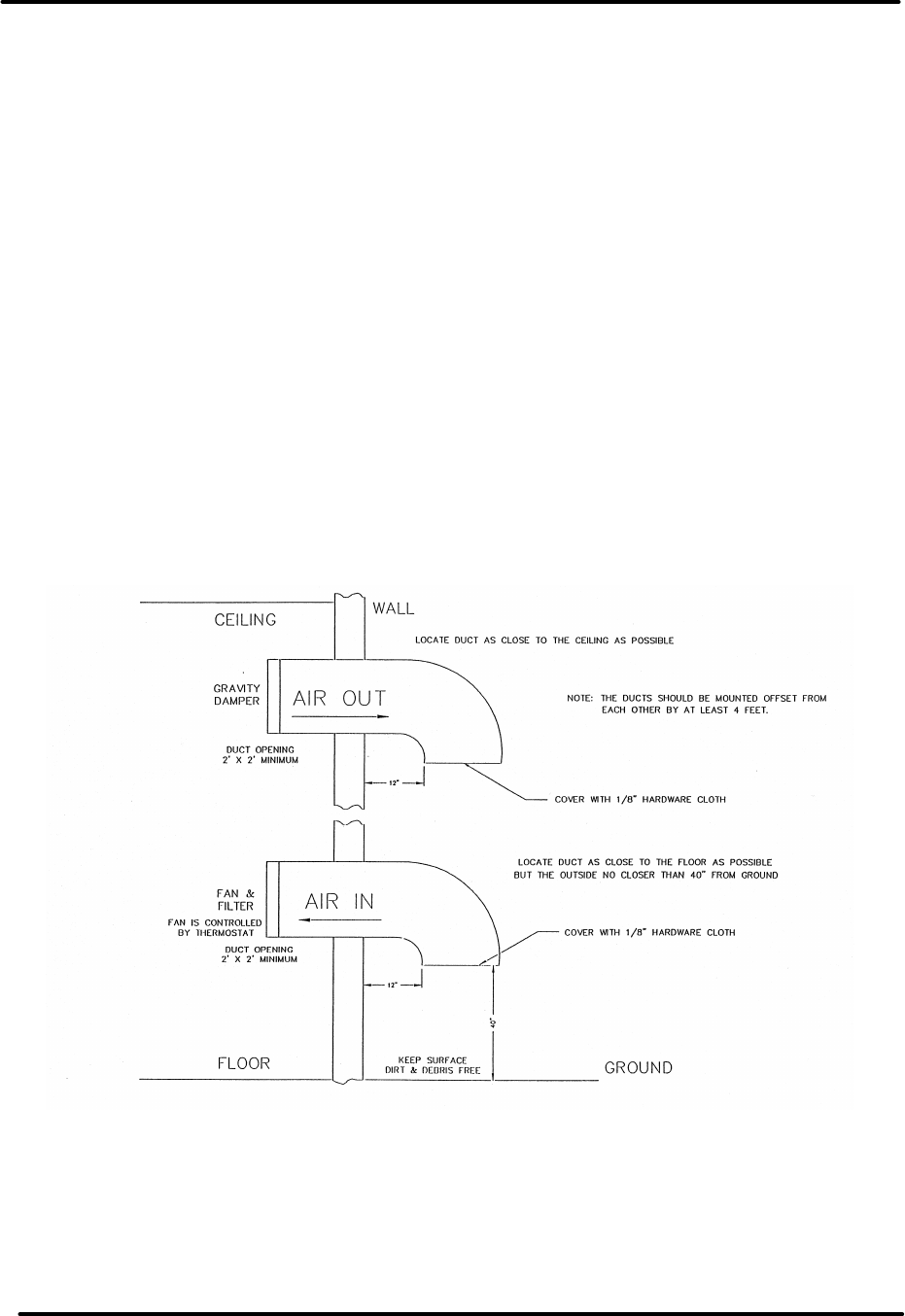
UHF Analog Driver/Transmitter/ Chapter 3, Site Considerations,
Translator Installation and Setup Procedures
LX Series, Rev. 3 3-4
12. Above 4000 feet, for external
venting, the air vent on the cabinet
top must be increased to an 8-inch
diameter for a 1 kW transmitter
and to a 10 inch diameter for 5 kW
and 6 kW transmitters. An
equivalent rectangular duct may be
used but, in all cases, the outlet
must be increased by 50% through
the outlet screen.
13. It is recommended that a site plan
be submitted to Axcera for
comments before installation
begins.
In calculating the blower requirements,
filter size, and exhaust size, if the total
load is known in watts, 2000 CFM into ½
inch of water will be required for each
5000 watts. If the load is known in BTUs,
2000 CFM into ½ inch of water will be
required for each 17,000 BTUs. The inlet
filter must be a minimum of seven square
feet, larger for dusty and remote
locations, for each 5000 watts or 17,000
BTUs. The exhaust must be at least four
square feet at the exhaust screen for
each 5000 watts or 17,000 BTUs.
The information presented in this section
is intended to serve only as a general
guide and may need to be modified for
unusually severe conditions.
A combination of air conditioning and
ventilation should not be difficult to
design (see Figure 3-1).
System interlocking and thermostat
settings should be reviewed with Axcera.
As with any equipment installation, it is
always good practice to consult the
manufacturer when questions arise.
Axcera can be contacted at (724) 873-
8100.
Figure 3-1. 1 kW Minimum Ventilation Configuration

UHF Analog Driver/Transmitter/ Chapter 3, Site Considerations,
Translator Installation and Setup Procedures
LX Series, Rev. 3 3-5
3.2 Unpacking the Chassis
w/modules, bandpass and trap
filters
Thoroughly inspect the cabinet, if
purchased, chassis with modules and all
other materials upon their arrival.
Axcera certifies that upon leaving our
facility the equipment was undamaged
and in proper working order. The
shipping containers should be inspected
for obvious damage that indicates rough
handling. Remove the cabinet, if
purchased, chassis and modules, along
with bandpass filter and trap Filter, from
the crates and boxes. Check for dents
and scratches or broken connectors,
switches, display, or connectors. Any
claims against in-transit damage should
be directed to the carrier. Inform Axcera
as to the extent of any damage as soon
as possible.
The modules are mounted to the chassis
assembly with slides that are on the top
and the bottom of the modules. There
are two thumb screws on the front panel
that hold each of the modules in place.
After placement of cabinet, all mounting
hardware, holding tray slides, shelving
and mounting plates inside the cabinet
should be checked for tightness. All
screws and bolts that are accessible
should be tightened initially when the
transmitter is received and periodically
thereafter if the transmitter is moved by
vehicle. All coaxial connectors, hard-line
connections and hardware holding
combiners, splitters, or any other
mounted items should be checked and
tightened. Check the front panel
thumbscrews that hold the Exciter/Driver
Sleds, Amplifier Module and Power
Supply Sleds in place are tight. This is
especially important after the transmitter
has been transported.
NOTE: Typically the transmitter is
shipped installed into a cabinet and the
following sections may be skipped.
3.3 Installing the Chassis w/modules
and filters
The chassis assembly is made to mount
in a standard 19” rack. The chassis
assembly mounts using the four #10
clearance mounting holes on the ends.
The chassis should be positioned; to
provide adequate air intake into the front
and the air exhaust of the fan(s) in the
rear; the ability to slide the modules out
for replacement purposes; the
installation of the bandpass filter and trap
filter; the coupler assembly; and output
transmission line. The chassis or cabinet
in which it is mounted should be
grounded using copper strapping
material.
NOTE: To remove the driver/power
amplifier module, mounted in the
exciter/driver assembly, the input and
output cables must be removed from the
rear of the module and also a 6/32” x ½”
Philips screw, mounted between the two
connectors, needs to be removed before
the module will pull out. After removal of
the screw, which is used to hold the
module in place during shipping, it does
not need to be replaced. (See Figure 3-2)
NOTE: To remove the Combiner Module,
found in the power amplifier assembly in
high power transmitters, the output cable
must be removed from the rear of the
module and also two 8/32” x ½” Philips
screws, mounted above the connector,
need to be removed before the module
will pull out. After removal of the screws,
which are used to hold the module in
place during shipping, they do not need
to be replaced.
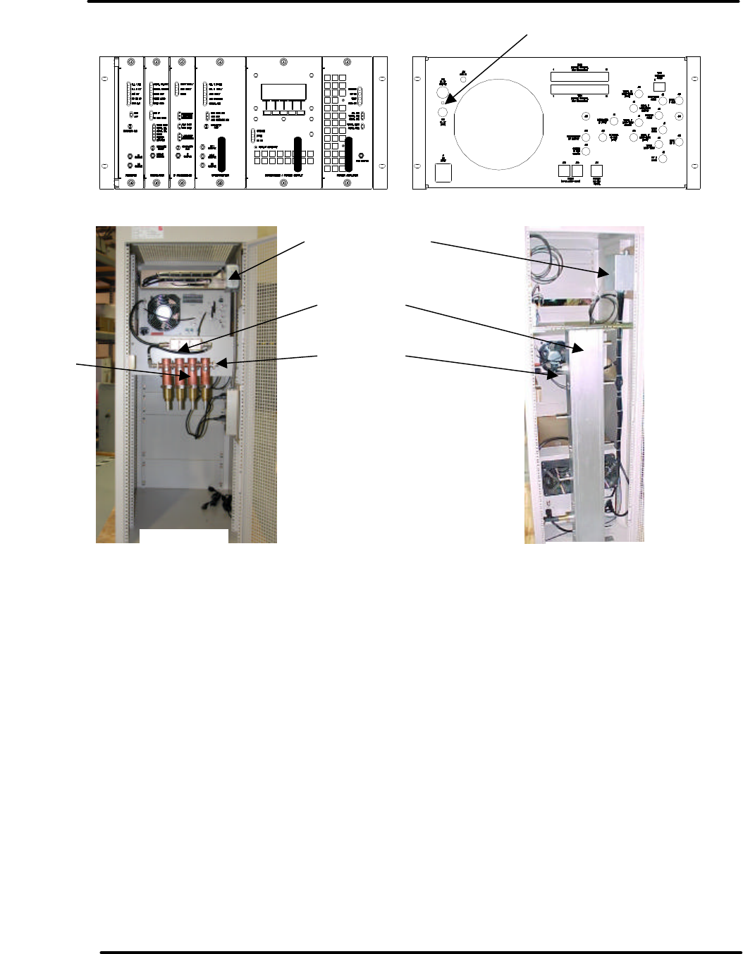
UHF Analog Driver/Transmitter/ Chapter 3, Site Considerations,
Translator Installation and Setup Procedures
LX Series, Rev. 3 3-6
Figure 3-2. Front and Rear View Reconnection Drawing
Connect the bandpass filter and trap filter
to the output of the chassis assembly.
Connect the transmission line for the
antenna system to the output of the trap
filter. A BNC sample jack of the output
on the trap filter can be used for test
purpose.
3.4 AC Input
Once the chassis and output connections
are in place, connect the AC power cord
from the chassis assembly of the 10 watt
or 100 watt transmitter to an AC outlet.
The AC input and current requirements
for LX Series transmitter/drivers are
provided in Table 3-1 at the beginning of
this chapter.
NOTES: The transmitter is factory set
for either 110 VAC or 220 VAC
operation as directed by customer.
Transmitters 250 Watts and above
use 220 VAC Input only.
Transmitters 4000 Watts and above
require two 220 VAC Inputs, one to
each cabinet.
All currents are with a Black picture.
The AC Input to the high power
transmitter connects to the terminal
block mounted in the AC input box
located toward the rear, right side near
the top of the cabinet. Connect the AC
Input Line 1 to Line 1 on the terminal
block, the AC Input Line 2 to Line 2 on
Trap Filter
Bandpass
Filter
Output to
Antenna
AC Input Box
Low Power
w/Cabinet High Power
Shipping Screw

UHF Analog Driver/Transmitter/ Chapter 3, Site Considerations,
Translator Installation and Setup Procedures
LX Series, Rev. 3 3-7
the terminal block and the AC Input
Ground to Ground on the terminal block.
Figure 3-3: AC Input Box Assembly
NOTE: An On/Off circuit breaker is
located on the rear of the
exciter/amplifier chassis near the AC
input jack. In high power
transmitters, one On/Off circuit is
located on the rear of the power
amplifier assembly for each power
supply assembly.
This completes the unpacking and
installation of the LX Series UHF
television transmitter. Refer to the setup
and operation procedures that follow
before applying power to the transmitter.
3.5 Setup and Operation
Initially, the transmitter should be turned
on with the RF output at the Trap Filter
terminated into a dummy load of at least
the power rating of the transmitter. If a
load is not available, check that the
output of the trap filter is connected to
the antenna for your system.
3.5.1 Input Connections
The input connections to the transmitter
or translator are to the rear of the
Chassis Assembly. NOTE: In dual exciter
systems input connections must be made
to the rear of both exciters.
Refer to the table and description that
follows for detailed information on the
input connections.
NOTE: If both the Receiver and
Modulator are present in your system
the Modulated IF output from the
Receiver or Modulator must be selected.
This is accomplished by connecting a low
or removing the low to TB31-Pin 3
located on the rear of the exciter/driver
assembly. By connecting the low, the
Modulator IF output is used by the IF
Processor module. By removing the low,
the IF from the internal or external
Receiver is used. (NOTE: The IF
Processor board must be configured for
external switching by placing jumper
W11 on J29 between pins 1 & 2).
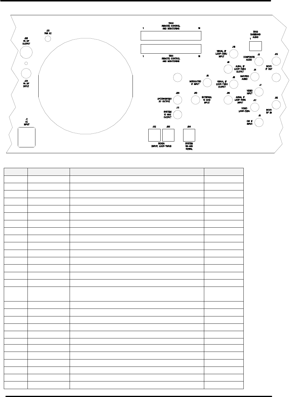
UHF Analog Driver/Transmitter/ Chapter 3, Site Considerations,
Translator Installation and Setup Procedures
LX Series, Rev. 3 3-8
Figure 3-4: Rear View of LX Series Analog Transmitter
Table 3-2: Rear Chassis Connections for the LX Series Analog Transmitter.
Port Type Function Impedance
J1 IEC AC Input N/A
TB02 Term Base Band Audio Input 600O
J3 BNC Composite Audio Input 75O
J4 BNC SAP / PRO Audio Input 50O
J5 BNC CW IF Input 50O
J6 BNC Modulated IF Input 50O
J7 BNC Video Input (Isolated) 75O
J8 BNC Visual IF Loop-Thru Output 50O
J9 BNC Aural IF Loop-Thru Output 50O
J10 BNC External 10 MHz Reference Input 50O
J11 BNC System 10 MHz Reference Output 50O
J12 BNC Receiver RF Input 50O
J13 BNC Receiver IF Output 50O
J14 RF Spare 2
J15 RF Spare 1
J17 BNC Video Loop-Thru (Isolated)
(May be connected to second exciter) 75O
J18 BNC Visual IF Loop-Thru Input 50O
J19 BNC Aural IF Loop-Thru Input 50O
J23 BNC Upconverter RF Output 50O
J24 BNC Power Amplifier RF Input 50O
J25 N Power Amplifier RF Output 50O
J32 RJ-45 SCADA (Input / Loop-Thru) CAT5
J33 RJ-45 SCADA (Input / Loop-Thru) CAT5
J34 RJ-45 System RS-485 Serial CAT5
TB30 Termination
Remote Control & Monitoring N/A
TB31 Termination
Remote Control & Monitoring N/A
J
1
J24
J25
J21
TB30
TB31
J32
J34
J33
J11
J10
J23
J6
J5
J19
J18
TB02
J13
J4
J7
J17
J8
J9
J12
J3
J15
SPARE
J14
SPARE

UHF Analog Driver/Transmitter/ Chapter 3, Site Considerations,
Translator Installation and Setup Procedures
LX Series, Rev. 3 3-9
3.5.2 Initial Turn On
Once the unit has been installed and all
connections have been made, the
process of turning on the equipment can
begin. First verify that AC power is
present and connected to the
transmitter. Verify all cables are properly
connected and are the correct type.
Once all of these things are done, the
unit is ready to be turned on following
the procedures below.
NOTE: In systems with two exciters and
an exciter switcher, repeat the following
procedure with Exciter B as the On Air
exciter. The exciter switcher must in
Manual.
Turn on the main AC power source that
supplies the AC to the transmitter. Check
that the AC power plug is connected to
J1 on the rear of the chassis assembly.
Check that the On/Off circuit breaker,
located on the rear of the Exciter/Driver,
is On. In high power transmitters, check
that the On/Off circuit breaker(s),
located on the rear of the Power
Amplifier Assembly(ies) are On.
Monitor the LCD display located on the
front of the control/monitoring module
as you proceed through this section.
When the transmitter is in the operate
mode, the STB menu appears. When in
the standby mode, the OPR menu
appears. Press the NXT key after each
menu to continue through the sequence.
3.5.2.1 (Optional) Receiver Module
LEDs on Front Panel
Fault Indicators:
PLL 1 FLT: This illuminates Red when
the Local Oscillator PLL is unlocked.
PLL 2 FLT: This illuminates Red when
the optional input frequency correcting
PLL is unlocked.
ALC FLT: This illuminates Red when the
ALC can not maintain output level.
Status Indicators:
DC ON I/P: This indicator will illuminate
Red when DC is applied to the RF input
center conductor.
MAN ALC: This illuminates Red when
the ALC can not maintain output level..
3.5.2.2 Modulator Module LEDs on
Front Panel
Fault Indicators:
AUR UNLOCK: This illuminates Red
when the Aural IF PLL is unlocked.
VIS UNLOCK: This illuminates RED
when the Visual IF PLL is unlocked.
AUD OV DEV: This indicator will
illuminate Red when the audio over-
deviates the aural carrier.
VIDEO LOSS: This indicates the loss of
Video to the modulator, when Red.
OVER MOD: This illuminates Red when
the video is over-modulated.
Status Indicators:
ALT IF CW: This indicates that there is
an external IF CW signal applied to the
Modulator
10MHz PRES: This indicates the
presence of a 10 MHz reference input.
3.5.2.3 IF Processor Module LEDs on
Front Panel
Fault Indicators:
INPUT FAULT: This illuminates Red if
the input to the module is missing or
low.
ALC FAULT: This illuminates RED when
the needed ALC value to maintain the
output level is beyond the range of the
circuitry.

UHF Analog Driver/Transmitter/ Chapter 3, Site Considerations,
Translator Installation and Setup Procedures
LX Series, Rev. 3 3-10
MUTE: This indicator will illuminate Red
when the transmitter is muted.
3.5.2.4 VHF/UHF Upconverter
Module LEDs on Front Panel
Fault Indicator:
AGC FAULT: This illuminates Red if the
required gain to produce the desired
output level is beyond the value set by
the AGC circuit. AGC out of range.
AGC OVERRIDE: This illuminates Red if
the drive to the driver module is too
high.
MAN GAIN: This illuminates Red if the
AGC is bypassed in Manual.
PLL 1: This illuminates Red if the 1 GHz
PLL is unlocked.
PLL 2: This illuminates Red if the 1.1-
1.9 GHz PLL is unlocked.
3.5.2.5 Controller Module LEDs on
Front Panel
Status Indicators:
OPERATE: This illuminates Green when
transmitter is in operate.
FAULT: This illuminates Red when a
fault has occurred in the transmitter.
DC OK: This illuminates Green when the
DC outputs that connect to the modules
in the transmitter are present.
3.5.2.6 Power Amplifier or Driver
Module LEDs on Front Panel
NOTE: Both the PA Module and
Driver Module have the same front
panel LEDs.
Status Indicators:
ENABLED: This illuminates Green when
the PA is in operate.
DC OK: This illuminates Green when the
DC inputs to the PA module are present.
TEMP: This illuminates Green when the
temperature of the heatsink in the PA is
below 78°C.
MOD OK: This illuminates Green when
the PA module is operating and has no
faults.
If the Module OK LED is Red and blinking
a fault is present. The meaning of the
blinking LED is as follows.
1 Blink: Indicates Amplifier Current
Fault.
2 Blinks: Indicate Temperature Fault.
3 Blinks: Indicate +32V Power Supply
Over Voltage Fault.
4 Blinks: Indicate +32V Power Supply
Under Voltage Fault.
5 Blinks: Indicate Reflected Power Fault.
6 Blinks: Indicate +12V or –12V Power
Supply Fault
3.5.3 Front Panel Screens for the
(Optional) Exciter Switcher Assembly
(Used in Dual Exciter Systems only)
The following screens are found on the 4
x 20 display located on the front of the
single channel exciter switcher tray.
NOTES: For automatic switching to the
back up exciter, the Error, Fault, Log in
the back up exciter must be cleared of all
Previous faults. Also, for remote control
of the exciter switcher, the exciter
switcher must be in Manual.
UHF Analog Driver/Transmitter/ Chapter 3, Site Considerations,
Translator Installation and Setup Procedures
LX Series, Rev. 3 3-11
Display Menu Screens for the (Optional) Exciter Switcher Tray
Table 3-3: Menu 01 - Splash Screen #1
This is the first of the two exciter switcher splash screens that is shown for the first few
seconds after reset or after pushing the SPL button on the Main Screen. Will
automatically switch to the second splash screen.
Table 3-4: Menu 02 - Splash Screen #2
This is the second of the two exciter switcher splash screens. Will automatically switch to
the Main Screen. The Name, Model Number, Code Version Number and Firmware
Number for your system are displayed on this screen. Make note of these two numbers
when conferring with Axcera on software problems.
Table 3-5: Menu 03 – Exciter Switcher Control Screen
This screen indicates that the exciter switcher is in automatic back-up and that Exciter A
is selected as the On Air Exciter. By selecting MANUAL the screen is shown as below.
Table 3-6: Menu 04 – Exciter Switcher Control Screen
This screen indicates that the exciter switcher is in Manual operation and that Exciter A is
selected as the On Air Exciter.
Table 3-7: Menu 05 – Exciter Switcher Control Screen
This screen indicates that there are 20 External Amplifiers reporting serial data in the
system. Also indicates that Exciter A is selected as the On Air Exciter and that the
system is in Manual, because the USE B option is present on the screen. By pushing the
button under USE B you are able to select Exciter B as the ON Air Exciter.
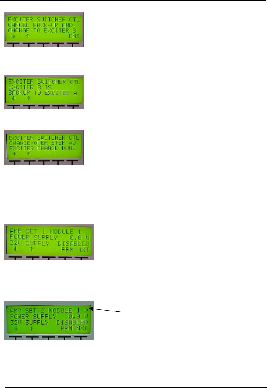
UHF Analog Driver/Transmitter/ Chapter 3, Site Considerations,
Translator Installation and Setup Procedures
LX Series, Rev. 3 3-12
Table 3-8: Menu 06 – Exciter Switcher Control Screen
This screen allows you to cancel the automatic back-up and that Exciter B is selected as
the On Air Exciter.
Table 3-9: Menu 07 – Exciter Switcher Control Screen
This screen indicates that Exciter B is selected as Back up to the On Air Exciter A.
Table 3-10: Menu 08 – Exciter Switcher Control Screen
This screen is only displayed when an exciter back up sequence is initiated. The backup
sequence runs through 10 steps that are displayed on 10 different screens. 9) Exciter
A/B On, 8) Disabling Exciter A, 7) Disabling Exciter B, 6) Changing Relay 1 of 2, 5)
Changing Relay 2 of 2, 4) Waiting for Relays, 3) Relay Change Done, 2) Enabling Exciter
A, 1) Enabling Exciter B; 0) Exciter Change Done. If a problem occurs during the
sequence it will stop on the screen where the problem occurred.
Table 3-11: Menu 09 – External Amplifier Status
These screens indicate the Status of the different Amplifier Modules. This screen is
monitoring the power supply for Module 1 in Amplifier Set 1. By arrowing down, the next
parameter for that module is viewed and these screens will continue for each individual
module in each Amplifier Set.
Table 3-12: Menu 10 – External Amplifier Status with Serial Link Error Icon
Serial Link Icon
Indicates that this module is not
present in your System or the
module may be present but no serial
communication commands are being
received from the device.
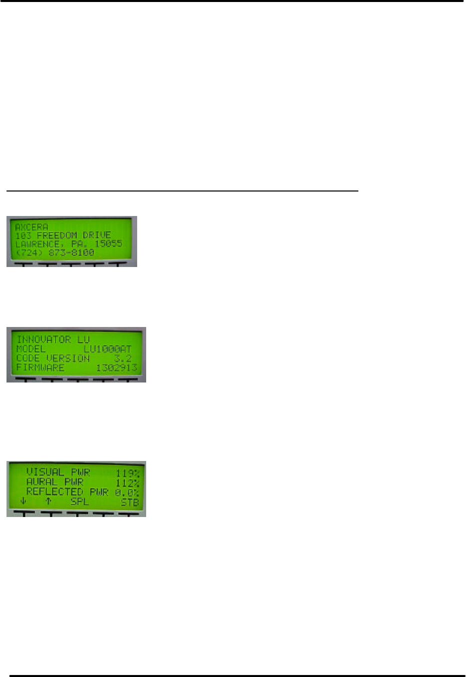
UHF Analog Driver/Transmitter/ Chapter 3, Site Considerations,
Translator Installation and Setup Procedures
LX Series, Rev. 3 3-13
3.5.4 Front Panel Screens for the
Exciter/Amplifier Chassis Assembly
A 4 x 20 display located on the front of
the Control & Monitoring/Power Supply
Module is used in the LX Series
transmitter for control of the operation
and display of the operating parameters
of the transmitter. Below are the typical
display screens for the system and may
vary depending on your system. The ↑
and ↓ characters are special characters
used to navigate up or down through the
menu screens. Display text flashes on
discrete fault conditions for all screens
that display a fault condition. When the
transmitter is in operate mode, the STB
menu appears. When the transmitter is
in standby mode, the OPR menu
appears.
NOTE: In systems with two exciters and
an exciter switcher the following screens
are typical on the exciter that is selected
as the On Air Exciter.
Display Menu Screens for the LX Series Transmitter/Translator
Table 3-13: Menu 01 - Splash Screen #1
This is the first of the two transmitter splash screens that is shown for the first few
seconds after reset or after pushing the SPL button on the Main Screen. Will
automatically switch to the second splash screen.
Table 3-14: Menu 02- Splash Screen #2
This is the second of the two transmitter splash screens. Will automatically switch to the
Main Screen. The Model Number, Code Version Number and Firmware Number for your
system are displayed on this screen. Make note of these two numbers when conferring
with Axcera on software problems.
Table 3-15: Menu 10 - Main Screen:
This is the default main screen of the transmitter. When the transmitter is in
operate, the 'STB' characters appear, allowing an operator to place the transmitter in
STANDBY, by pushing the right most button located under to display. When the
transmitter is in standby the 'STB' characters are replaced with 'OPR' and the forward
power values are displayed as OFF. An operator can change the transmitter from
STANDBY to OPERATE by pressing the right most button on the front panel display. If the
transmitter is in operate mode but off due to a modulation fault, the display reports the
system power as Auto Off. Pushing the SPL button will display the two splash screens.
If the ↓ key is activated the display changes to Menu 11, the System Error List Access
Screen. If the ↑ key is activated the display changes to Menu 13, the Transmitter
Configurations Access Screen.
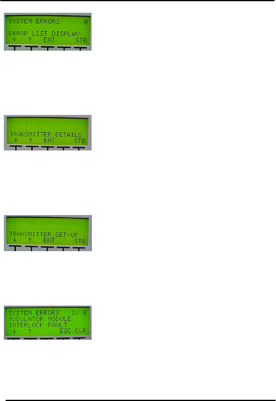
UHF Analog Driver/Transmitter/ Chapter 3, Site Considerations,
Translator Installation and Setup Procedures
LX Series, Rev. 3 3-14
Table 3-16: Menu 11 - Error List Access Screen
This screen of the transmitter shows the current number of system errors, displayed in
upper, right of screen, shown above is System Errors 0. and provides operator access to
view Menu 20, the error list screens, by pushing the ENT button if errors are indicated. .
If the ↓ key is pushed the display changes to Menu 12, Table 3-17, the Transmitter
Device Data Access Screen. If the ↑ key is activated the display returns to Menu 10, the
Main Screen. When ENT is pushed, if errors are present, Menu 20, Table 3-19, the
System Error List Display Screen is displayed with the error indicated.
Table 3-17: Menu 12 - Transmitter Device Data Access Screen
This screen of the transmitter allows access to various parameters of the transmitter
system. This is the entry point to Menu 30, the System Details Screens, by pausing the
ENT button. When the ENT button is pushed, Menu 30 is accessed. Go to Menu 30, Table
3-22 for set up details. Before pushing the ENT button: if the ↓ key is activated the
display changes to Menu 13, Transmitter Configurations Access Screen. If the ↑ key is
activated the display returns to Menu 11, the Error List Access Screen.
Table 3-18: Menu 13 - Transmitter Configuration Access Screen
This screen of the transmitter allows access to various software settings of the
transmitter system. If ENT is pushed, go to Menu 40, Table 3-23, the access to
transmitter configuration and set up. Before pushing the ENT button: if the ↓ key is
activated the display returns to Menu 10, Main Screen. If the ↑ key is activated the
display returns to Menu 12, the Transmitter Device Data Access Screen.
Table 3-19: Menu 20 - Error List Display Screen
When ENT is pushed on the Error List Access Screen, Menu 11, if errors are present,
Menu 20, the System Error List Display Screen is displayed with the System Error
indicated as shown above. This screen of the transmitter allows access to the system
faults screens. Fault logging is stored in non-volatile memory. The transmitter's
operating state can not be changed in this screen. The 'CLR' switch is used to clear
previously detected faults that are no longer active. The ↑ key and ↓ key allow an
operator to scroll through the list of errors that have occurred. The ESC button is used to
leave this screen and return to Menu 11, Table 3-16, the Error List Access Screen.
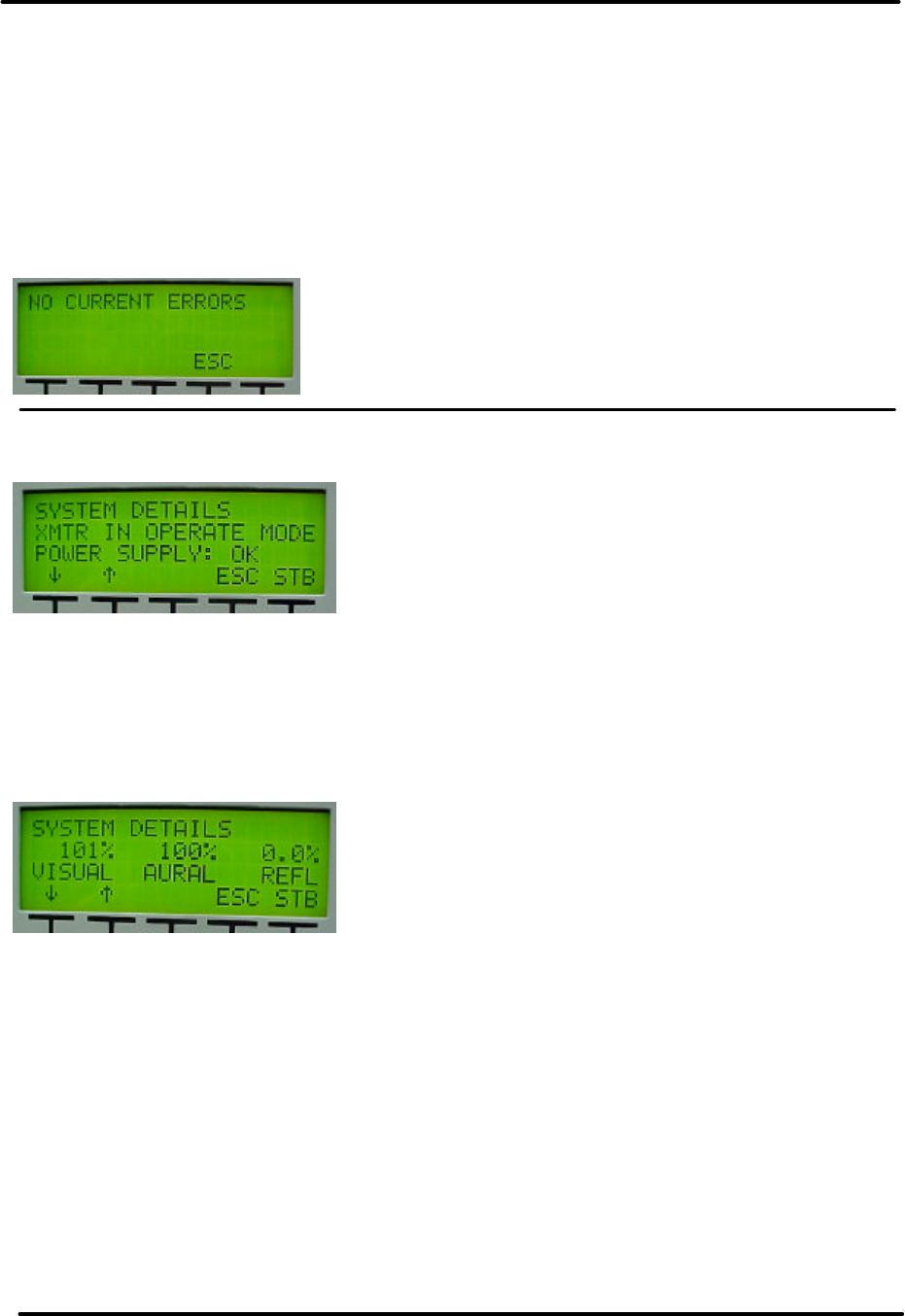
UHF Analog Driver/Transmitter/ Chapter 3, Site Considerations,
Translator Installation and Setup Procedures
LX Series, Rev. 3 3-15
The screen shown indicates a Modulator Module Interlock Fault, typically because the
Modulator is not present. It also indicates that there are a total of eight faults. The
other faults can be displayed by pushing the ↓ key button. To clear the displayed System
Error, fault, that is no longer active, push the button under CLR. Repeat to clear each
additional displayed System Error. If an error is active it will not clear.
NOTES: In Dual Exciter Systems with an Exciter Switcher, for the automatic switching to
the back up exciter to occur, the System Error, Fault, Log located in the Back Up Exciter
must be cleared of all Previous Faults, as described above.
With all Errors, faults, cleared the screen below should be displayed. Push the button
under ESC to return to Menu 11, Table 3-16, the Error List Access Screen.
Menu 30 is entered by selecting ENT at Menu 12, Table 3-7.
Table 3-20: Menu 30 - Transmitter Device Details Screen
This screen allows access to the transmitter parameters of installed devices. The system
is configured to know which devices are present. Current values for all installed devices
are shown. If a module is not installed, only a "MODULE NOT PRESENT" message will be
displayed. The first screen displayed is Menu 30-1, Table 3-21, the System Details
Screen.
Table 3-21: Menu 30-1 – System Details Screen
The ↓ and ↑ arrows allow you to scroll through the different parameters of each device as
shown in Table 3-22 that follows. Each System Component is a different screen. The
proper IF Processor and the Driver or the Power Amplifier will be programmed for your
system. The External Amplifier Modules will only be used in high power transmitters.
Examples of External Amplifier Modules displays are: (AMP SET 1 MODULE 1) and (AMP
SET 2 MODULE 4).
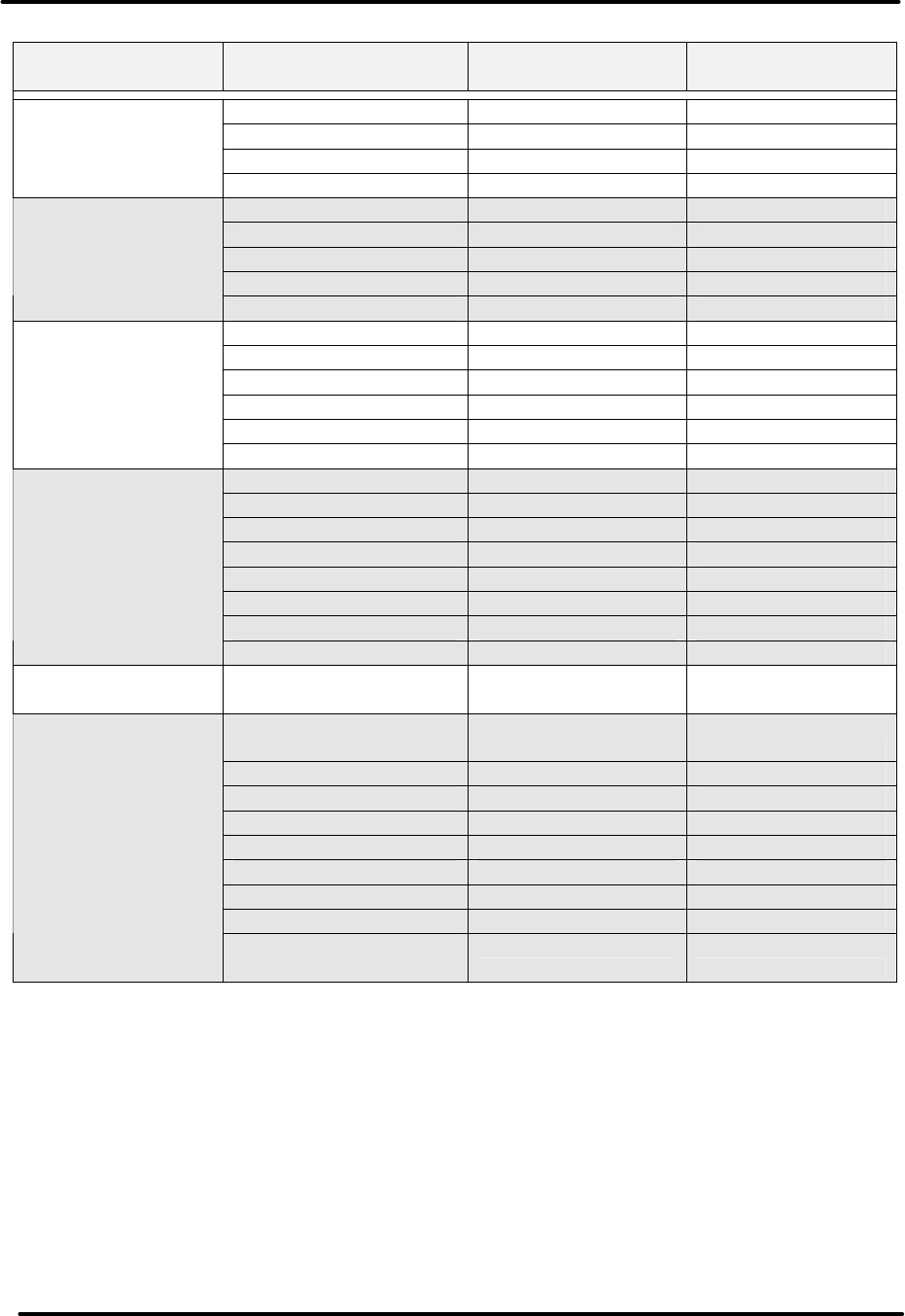
UHF Analog Driver/Transmitter/ Chapter 3, Site Considerations,
Translator Installation and Setup Procedures
LX Series, Rev. 3 3-16
Table 3-22: Transmitter Device Parameters Detail Screens
System
Component Parameter Normal Faulted (Blinking)
AFC 1 LEVEL 0 - 10.00 V N/A
PLL 1 CIRCUIT LOCKED UNLOCKED
ALC INPUT OK FAULT
Receiver Details
(Not used with
transmitter.) FAULT AT 0 - 10.00 V FAULT
PLL CIRCUIT LOCKED UNLOCKED
OUTPUT LEVEL .24 – 1.00 V N/A
AURAL DEVIATION 0 - 125 kHz N/A
CW INPUT PRESENT NOT USED
Modulator Details
(May Not be used
with receiver.) CALL SIGN NONE N/A
INPUT SIGNAL STATE OK FAULT
MODULATION OK FAULT
INPUT IF MODULATOR or J6 N/A
DLC CONTROL LOCK 0 - 5.00 V N/A
ALC LEVEL 0 - 5.00 V N/A
IF Processor
Details
(Analog Systems)
ALC MODE AUTO or MANUAL N/A
AFC 1 LEVEL 0 – 5.00 V N/A
AFC 2 LEVEL 0 - 5.00 V N/A
CODE VERSION x.x N/A
PLL 1 CIRCUIT LOCKED FAULT
PLL 2 CIRCUIT LOCKED FAULT
AGC 1 LEVEL 0 - 5.00 V N/A
AGC 2 LEVEL 0 - 5.00 V N/A
Upconverter
Details
INT. 10 MHz IS USED N/A
System Control
Details SUPPLY ENABLED
FOR xxx HOURS N/A
POWER SUPPLY
STATE, 32V 32 VDC N/A
±12V SUPPLY OK or OFF FAULT
FORWARD POWER xxx% xxx%
REFLECTED POWER xxx% xxx%
AMP 1 CURRENT xx.xA xx.xA
AMP 2 CURRENT xx.xA xx.xA
TEMPERATURE xxC xxC
CODE VERSION x.x N/A
Driver and PA
Details
PA HAS OPERATED
FOR xxx HOURS N/A
UHF Analog Driver/Transmitter/ Chapter 3, Site Considerations,
Translator Installation and Setup Procedures
LX Series, Rev. 3 3-17
System
Component Parameter Normal Faulted (Blinking)
POWER SUPPLY
VOLTAGE, 32V 31 – 32 VDC N/A
32V SUPPLY ENABLED or
DISABLED FAULT
FORWARD POWER xxx% xxx%
REFLECTED POWER xxx% xxx%
AMP CURRENT 1 xx.xA xx.xA
AMP CURRENT 2 xx.xA xx.xA
AMP CURRENT 3 xx.xA xx.xA
AMP TEMPERATURE xxC xxC
CODE VERSION x.x N/A
Ext. Power
Amplifier Modules
Details (Only in
high power
systems).
Will indicate Amp
Set and Module
within the Set.
Will step through
each Set and
Module. PA HAS OPERATED
FOR xxx HOURS N/A
Pushing the ↓ Down Arrow, after scrolling through all the detail screens, will put you back
to Menu 30, Table 3-20. Push the ESC button to exit the Transmitter Device Parameter
Screens to Menu 12, Table 3-17 to the Transmitter Device Parameter Access Screen.
Menu 40 (Table 3-23) is entered by selecting ENT at Menu 13.
Table 3-23: Menu 40 - Authorized Personnel Screen
This screen of the transmitter notifies an operator that they are only to proceed if they
are authorized to make changes to the transmitter's operation. Changes made within the
following set-up screens can affect the transmitters output power level, output frequency,
and the general behavior of the transmitter. Please do not make changes within the
transmitter's set-up screens unless you are familiar with the operation of the transmitter.
This screen is implemented in transmitter software version 1.4 and above.
Pressing ENT will put you into the Transmitter Set Up Screens for Menu 40.
A safeguard is added to the Set Up Menus in software version 2.5 and above. If a change
is made to a screen within the Set Up Menus, when you go to the next menu, a new
screen asks if you accept the change or want to return to the previous menu to
reconsider the changes made.
To accept the changes, the two buttons located under ACCEPT must be pushed
simultaneously.
To return to the previous Menu to make corrections, the two buttons located under the
RETURN must be pushed simultaneously.
Upon returning to the previous Menu the correct input must be entered and the above
procedure repeated, this time accepting the changes
UHF Analog Driver/Transmitter/ Chapter 3, Site Considerations,
Translator Installation and Setup Procedures
LX Series, Rev. 3 3-18
Accept or Return to previous Menu Screen
Pushing these two buttons Pushing these two buttons
Simultaneously will accept Simultaneously will return you
the change. to the previous Menu.
The Set Up Screens are shown in Table 3-25 Menu 40-1 through Table 3-42 Menu 40-18
that follow.
Table 3-24: Menu 40-1 - Transmitter Set-up: Power Control Screen
This screen of the transmitter is the first of several that allows access to transmitter set-
up parameters. This is the output Power Control Screen. When + is selected, the Power
will increase. When - is selected, the Power will decrease.
Table 3-25: Menu 40-2 - Transmitter Set-up: Model Select Screen
This screen is used to specify which components are expected to be part of the system.
By specifying the model number, the transmitter control firmware knows which
components should be installed and it will be able to display faults for components that
are not properly responding to system commands.
Table 3-26: Menu 40-3 - Transmitter Set-up: Receiver Channel Configuration
This screen of the transmitter allows access to transmitter frequency set-up parameters.
The choices of this screen are as follow. NOTE: The above screen will only be present if a
Receiver is part of the system. Used to set the Receiver Channel designation and for
custom Channel Offsets the setting of the PLL operating frequency.
UHF Analog Driver/Transmitter/ Chapter 3, Site Considerations,
Translator Installation and Setup Procedures
LX Series, Rev. 3 3-19
Table 3-27: Menu 40-4 - Transmitter Set-up: Upconverter Channel Select Screen
The choices of this screen are to the standard UHF / VHF channels. The + and – buttons
change the desired channel of the transmitter. The PLL frequency is set for custom
Offsets within the upconverter frequency. Any change to the channel is immediately set
to the LO / Upconverter Frequency Synthesizer PLL circuit.
Table 3-28: Menu 40-5 - Transmitter Set-up: Serial Address Screen
This screen allows the user to set the serial address of the transmitter. The default
address is 5. This value and all other set-up parameters, are stored in non-volatile
memory.
Table 3-29: Menu 40-6 - Transmitter Set-up: Station ID Screen
This screen allows the user to set the Station ID, Call Sign, in analog transmitters. If
blank characters are used for all five positions, then the Station ID feature is disabled.
Otherwise the Station ID code is transmitted every 15 minutes. This value and all other
set-up parameters, are stored in non-volatile memory. (NOTE: If an external Receiver
Tray is used in your system, the LX Series Station ID is disabled. Therefore, the Station
ID must be set up in the external Receiver Tray.)
Table 3-30: Menu 40-7 - Transmitter Set-up: System Visual Power Calibration
This screen is used to adjust the calibration of the system's visual power. A symbol
placed under the '6' character is used to show major changes in the calibration value.
When the calibration value is at full value, the character will be full black. As the value
decreases, the character pixels are gradually turned off. The calibration value is a value
between 0 and 255 but the calibration value symbol only has 40 pixels. Therefore small
changes in actual calibration value may not affect the symbol's appearance.
UHF Analog Driver/Transmitter/ Chapter 3, Site Considerations,
Translator Installation and Setup Procedures
LX Series, Rev. 3 3-20
Table 3-31: Menu 40-8 - Transmitter Set-up: System Aural Power Calibration
This screen is used to adjust the calibration of the system's aural forward power. A
calibration value symbol is used for this screen as on the previous screen.
Table 3-32: Menu 40-9 - Transmitter Set-up: System Reflected Power Calibration
This screen is used to adjust the calibration of the system's reflected power. Again a
calibration value symbol is used for this screen as on the previous screens.
Table 3-33: Menu 40-10 - Transmitter Set-up: Modulated Output Calibration
In analog systems this screen is used to adjust the calibration of the system's modulated
output signal detector. The calibration value symbol is again used to graphically
represent the modulated output signal detector's calibration value.
Table 3-34: Menu 40-11 - Transmitter Set-up: Aural Deviation Calibration
In analog systems this screen is used to adjust the calibration of the system's aural
deviation detector. The calibration value symbol is again used to graphically represent
the aural deviation detector's calibration value.
Table 3-35: Menu 40-12 - Transmitter Set-up: Forward Power Fault Threshold Screen
This screen is used to set the minimum forward power fault threshold. When the
transmitter is operating, it must operate above this value otherwise the system will shut
down with fault for 5 minutes. If after five minutes the fault is not fixed, the transmitter
will enable, measure power less than this value and again shut down for five minutes.
UHF Analog Driver/Transmitter/ Chapter 3, Site Considerations,
Translator Installation and Setup Procedures
LX Series, Rev. 3 3-21
Table 3-36: Menu 40-13 - Transmitter Set-up: Reflected Power Fault Threshold
This screen is used to set the maximum reflected power fault threshold. When the
transmitter is operating, it must not operate above this value otherwise the system will
slowly begin to reduce the forward output power. If the system's reflected output power
exceeds the maximum reflected power threshold by five percent or more, the transmitter
will shut down with fault for 5 minutes. If after five minutes the fault is not fixed, the
transmitter will enable, measure power above this value plus five percent and again shut
down for five minutes. If the system's reflected output power exceeds the maximum
reflected power threshold due to some condition like the formation of ice on an antenna,
the transmitter reduces forward power to a level where the reflected power is less than
this threshold. The transmitter will automatically increase its output power to normal
operation when the cause of higher than normal reflected power is corrected.
Table 3-37: Menu 40-14 - Transmitter Set-up: Auto Stand-By Control
Certain LX transmitter locations are required to reduce to no output power on the loss of
video input. When a LX transmitter is configured for Auto Stand-By On Modulation Loss,
the transmitter will switch to stand-by, if a modulated input signal fault is detected by the
IF Processor module that lasts for more than ten seconds. Once the modulated input
signal fault is cleared, a transmitter in operate mode will return to normal operation. This
feature is implemented in transmitter software version 1.4 and above.
Table 3-38: Menu 40-15 - Transmitter Set-up: Receiver ALC Fault Set Up
This screen is used to set up the level of the ALC at which the Receiver will fault. This
feature is implemented in transmitter software version 2.0 and above. NOTE: The above
screen will only be present if a Receiver is part of the system.
Table 3-39: Menu 40-16 - Transmitter Set-up: Inner Loop Gain Control
This screen is used to set up the Inner Loop Gain of the exciter/amplifier assembly. This
feature is implemented in transmitter software version 2.0 and above

UHF Analog Driver/Transmitter/ Chapter 3, Site Considerations,
Translator Installation and Setup Procedures
LX Series, Rev. 3 3-22
Table 3-40: Menu 40-17 - Transmitter Set-up: Optional System Control
This screen is used to set up any optional system, including the addition of the optional
Modulator in a translator system. This feature is implemented in transmitter software
version 2.0 and above.
Table 3-41: Menu 40-18 - Transmitter Set-up: Remote Commands Control
This screen is used to allow or deny the use of remote control commands. When
disabled, remote commands are not used. Remote commands are commands received
either through the rear terminal blocks or through serial messages.
Push the ESC button to exit the Transmitter Set Up Screens to Menu 13, Table 3-18, the
Transmitter Configuration Access Screen.
This completes the description of the menu screens for the LX Series exciter/amplifier
chassis assembly.
3.5.5 Operation Procedure
If necessary, connect the transmitter to
the antenna. Check that the output is
100% and if needed adjust the ALC
Gain adjust pot on the front panel of
the IF Processor to attain 100%. The
power raise / lower settings, in the
menus, are only to be used for
temporary reductions in power.
The power set-back values do not
directly correspond to the output power
of the transmitter.
This completes the Installation, Set Up
and Turn On of the Driver/Transmitter.
NOTES: In dual exciter systems,
repeat the above procedure with
Exciter B selected as the On Air
exciter. For remote control of the
exciter switcher, the exciter switcher
must be in Manual.
For automatic switching to the back up
exciter, the Error, Fault, Log in the
back up exciter must be cleared of all
previous System Errors, faults.
If a problem occurred during the setup
and operation procedures, refer to
Chapter 5, Detailed Alignment
Procedures, of this manual for more
information.

UHF Analog Driver/Transmitter/ Chapter 4, Circuit Descriptions
Translator
LX Series, Rev. 3 4-1
Chapter 4
Circuit Descriptions
4.0 (Optional) Exciter Switcher Tray,
(110 VAC 1305727 or 220 VAC
1305715); Appendix B)
NOTE: Part of a dual exciter system.
4.0.1 Exciter Switcher Control Board
(220 VAC 1305704 or 110 VAC
1305725; Appendix B)
The Exciter Switcher Control Boards for
220 VAC and 110 VAC are the same
except for the location of the T1
transformer. Location T1-110 is used
with 110VAC input and location T1-230
is used with 230VAC input. Refer to the
schematic for the board 1305705 Page 3
of 4, located in Appendix B, for a visual
representation of the wiring.
The Exciter Switcher Control Board
monitors and controls both Exciters and
controls automatic switching of the
Exciters in case of malfunction in the On-
Air Exciter using a coaxial relay. ICs on
the board monitor the operating
parameters of the Exciters and determine
if the Exciters are functioning properly.
The front panel of the Exciter Switcher
has an LCD display, which provides set
up screens for the operation of the
switching process.
The coaxial relay has four “N” connectors
that provide input and output
connections to the relay. The RF Output
from Exciter “A” connects to J21. The RF
Output from Exciter “B” connects to J23.
The Selected Exciter RF Output to the
external amplifiers connects to J24. The
Exciter “A/B” Load connects to J22, to
which the RF output of the Off Air Exciter
is connected. An internal wire harness
connects the relay to J14 on the Exciter
Switcher Control Board. These
connections provide the control voltages
to the relay from the control board and
status indication connections back to the
control board.
4.1 (Optional) (A1) Receiver Module
(VHF LB 1304000, VHF HB 1304001 or
UHF 1304002; Appendix B)
NOTE: Not present in a transmitter
system.
4.1.1 IF ALC Board (1304003;
Appendix B) Used in the VHF LB
1304000, VHF HB 1304001 and UHF
1304002 Receiver Assemblies
The board provides the interface between
the receiver and the backplane and also
contains the control and ALC circuits for
the sled.
The control portion of the board consists of
a microcontroller (U8) and its associated
components that communicate to the
outside world via an RS-485 serial data
link. The microcontroller receives various
metering and alarm functions such as AFC
and ALC voltages, PLL and ALC faults and
communicates them back to the system
controller for display on the transmitter’s
LCD display. It also receives the channel
information from the system controller,
and converts it to the programming data
for the PLL chip on the Mixer/PLL Board in
the receiver.
The IF portion of the board consists of an
input pin attenuator, which is used to
normalize the gain of the board to account
for variations in the input level to the
board. The pin attenuator consists of
DS1, DS2 and associated components.
The signal is then amplified by U2-U4 and
associated components and applied to a
SAW filter that rejects any out of channel
signal that made it through the receivers
RF front end. Amplifiers U5, U6 and their
associated components are used to
amplify the signal to make up for the loss
through the filter. The final output of U6 is
split by a lumped element Wilkinson
splitter consisting of C21, C26, C27, L12,
and L14. The output from one of the
output ports is sent to the output of the

UHF Analog Driver/Transmitter/ Chapter 4, Circuit Descriptions
Translator
LX Series, Rev. 3 4-2
receiver, and the other output is
connected to a peak detector and used
by the ALC. The ALC circuit, consisting
of U1, CR4 and its associated
components, varies the gain of the pin
attenuator on the front end of the board
to maintain a constant output level. The
pin attenuator has an overall adjustment
range of approximately 50 dB.
There is a comparator that looks at the
pin attenuator voltage and generates an
alarm if the pin attenuator is close to
running out of range. This alarm is
likely to occur if the RF input signal to
the receiver is weak or missing. This
alarm is received by the microcontroller
that passes it along to the transmitter's
system controller, which mutes the
signal in the IF processor until the fault
goes away.
4.1.2 UHF Mixer/PLL Board
(1304021; Appendix B) Used in the
UHF 1304002 Receiver Assembly
OR VHF Mixer/PLL Board (1304013;
Appendix B) Used in the VHF LB
1304000 and VHF HB 1304001 Receiver
Assemblies
Both the VHF and UHF Mixer/PLL Boards
operate the same except for where
indicated in the description. This board
converts the RF input to the receiver to
a 44 MHz IF. It consists of a Mixer, a
local oscillator and some IF amplifiers
used to make up for the loss of the
mixer.
The Local oscillator signal is generated
by the VCO (U3), which operates directly
at the LO frequency of the channel
center frequency (400-800 MHz UHF or
(104-176 MHz VHF) + 44 MHz. The
oscillator is phase locked to a 10 MHz
standard by U2, U8, and their associated
components. TP1 shows the AFC
voltage, which is also sent back to the IF
ALC board to be displayed on the system
level controller. The variable resistor
R30 sets the LO output level to +10
dBm into the mixer U4. This is done by
looking at the LO sample at J2 with a
spectrum analyzer, adjusting R30 until the
level is -10 dBm. This ensures that the
mixer gets the correct level, as the sample
is 20 dB down from the level into the
mixer.
Mixer U4 converts the RF input at J1 to an
IF frequency of 44 MHz. L13, L14 and
C56 form a low pass filter, which rejects
any unwanted higher frequency
conversion products. U5 and U9 amplify
the signal, which exits the board at J5.
There are two jumpers on J3 and J4 that
allow the user to switch in a 10 dB
attenuator if the input level to the receiver
is too high. Normally the jumpers are
connected between pins 1 and 2 of each
connector, but if the user has a high input
level, they can be switched to connect
pins 2 and 3 of each connector, which
switches in the 10 dB pad.
The A/V ratio of the incoming signal can
be adjusted via an external front panel
pot, which controls the bias on pin
attenuator DS3. The pin attenuator
controls the Q of a notch set at the aural
IF carrier frequency, set by C41 and L7.
The A/V ratio control is used if the
incoming signal has an aural carrier that is
too high relative to the visual carrier.
4.1.3 UHF Preamplifier Board
(1304092; Appendix B) Used in the UHF
1304002 Receiver Assembly
OR VHF Low Band Preamplifier Board
(1305213; Appendix B) Used in the VHF
LB 1304000 Receiver Assembly
OR VHF High Band Preamplifier Board
(1303878; Appendix B) Used in the VHF
HB 1304001 Receiver Assembly
The VHF Low Band, VHF High Band and
UHF Preamplifier Boards operate the same
except for where indicated in the
description.
This board filters and amplifies the low
level RF input signal to the receiver. It
consists of two two-pole bandpass filters

UHF Analog Driver/Transmitter/ Chapter 4, Circuit Descriptions
Translator
LX Series, Rev. 3 4-3
and a dual stage preamplifier. The
filters are tuned at the RF channel
frequency and are about 8 MHz wide.
They are intended to filter off the
unwanted image product 88 MHz below
the Channel center frequency. Each
filter is a combination micro-strip
lumped element filter. The center
frequency of the filter is set byC10 and
C11 for the input filter and C20 and C21
for the output filter on the UHF
preamplifier. The center frequency of
the filter is set by C6, C8 and C10 for
the input filter, and C26, C28 and C30
for the output filter on the VHF LB
preamplifier. The VHF HB has no
adjustments for the input and output
filters.
The input filter also has provisions to
insert a +12V DC signal onto the center
conductor of the receiver's RF input to
power an external preamp. The jumper
W1 on J2 controls whether or not the DC
bias is applied to the center conductor.
When it is connected between pins 1 and
2, the +12V bias is applied. When it is
between pins 2 and 3, there is no bias
applied. The presence of the DC bias is
displayed on a front panel LED on the
sled.
CAUTION: Do not hook up the RF
input to any test equipment with the
DC bias applied. Always move the
jumper W1 on J2 to the Bias off
position, between pins 2 & 3, to
prevent possible damage to the test
equipment.
The amplifier consists of two cascaded
stages, which provide approximately 27
dB of gain across the VHF LB, VHF HB or
UHF band.
4.2 (A2) Modulator Module
(1301929; Appendix B)
NOTE: May not be present in a translator
system.
4.2.1 Analog Modulator Board
(1301797; Appendix B)
The board takes the audio and video inputs
and produces a modulated visual IF +
aural IF output.
Main Audio and Aural IF portion of the
board
The analog modulator board takes each of
the three possible audio inputs and
provides a single audio output.
4.2.1.1 MONO, Balanced Audio Input
The first of the three possible baseband
inputs to the board is a 600Ω, balanced-
audio input (0 to +10 dBm) that enters
through jack J41A, pins 10A (+), 12A
(GND), and 11A (-), and is buffered by
U11A and U11B. Diodes CR9, CR10, CR12
and CR13 protect the input to U11A and
U11B if an excessive signal level is present
on the input. The outputs of U11A and U1B
are applied to differential amplifier U11C.
U11C eliminates any common mode signals
(hum) on its input leads. A pre-emphasis
of 75 µs is provided by R97, C44, and R98
and can be eliminated by removing jumper
W6 on J22. The signal is then applied to
amplifier U11D whose gain is controlled by
jumper W7 on J23. Jumper W7 on jack
J23 is positioned according to the input
level of the audio signal (0 or +10 dBm). If
the input level is approximately 0 dBm, the
mini-jumper should be in the high gain
position between pins 1 and 2 of jack J23.
If the input level is approximately +10
dBm, the mini-jumper should be in low
gain position between pins 2 and 3 of jack
J23. The balanced audio is then connected
to buffer amplifier U12A whose input level
is determined by the setting of the MONO,
balanced audio gain pot R110, accessed
through the front panel. The output of the
amplifier stage is wired to the summing
point at U13C, pin 9.
4.2.1.2 STEREO, Composite Audio Input
The second possible audio input to the
board is the composite audio (stereo) input

UHF Analog Driver/Transmitter/ Chapter 4, Circuit Descriptions
Translator
LX Series, Rev. 3 4-4
that connects to the board at J41A Pin
14A (+) and J41A Pin 13A (-).
NOTE: For the transmitter to operate
using the composite audio input the
Jumper W1 on J4 must be between Pins
2 and 3, the Jumper W2 on J6 must be
between Pins 2 and 3 and the Jumper W4
on J5 must be between Pins 1 and 2.
These jumpers connect the composite
audio to the rest of the board.
Jumper W14 on jack J26 provides a 75Ω
input impedance when the jumper is
between pins 1 and 2 and a high
impedance when it is between pins 2 and
3. The Diodes CR17, CR18, CR20 and
CR21 protect the input stages of U14A
and U14B if an excessive signal level is
applied to the board. The outputs of
U14A and U14B are applied to the
differential amplifier U13A, which
eliminates common mode signals (hum)
on its input leads. The composite input
signal is then applied to the amplifier
U13B, whose gain is controlled by the
STEREO, composite audio gain pot R132,
accessed through the front panel. The
composite audio signal is then connected
to the summing point at U13C, pin 9.
4.2.1.3 SAP/PRO, Subcarrier Audio Input
The third possible input to the board is
the SAP/PRO, SCA audio input at J41A
pin 16A(+) and 17A(-). The SCA input
has an input matching impedance of 75Ω
that can be eliminated by removing the
jumper W15 from pins 1 and 2 on J28.
The SCA input is bandpass filtered by
C73, C74, R145, C78, C79, and R146 and
is fed to the buffer amplifier U13D. The
amplified signal is then applied though
the SAP/PRO, SCA gain pot R150,
accessed through the front panel, to the
summing point at pin 9 of U13C.
4.2.1.4 Audio Modulation of the
4.5 MHz VCO
The Mono balanced audio, or the Stereo
composite audio, or the SAP/PRO SCA
buffered audio signal, is fed to the
common junction of resistors R111,
R130, and R152 that connect to pin 9 of
amplifier U13C. The output audio signal at
pin 8 of U13C is typically .8 Vpk-pk at a
±25 kHz deviation for Mono balanced audio
or .8 Vpk-pk at ±75 kHz deviation for
Stereo composite audio as measured at the
Test Point TP1. This audio deviation signal
is applied to the circuits containing the 4.5
MHz aural VCO U16. A sample of the aural
deviation level is amplified, detected by
U15A and U15B, and connected to J41A pin
5A on the board. This audio-deviation
level is connected to the front panel LCD
display on the Control/Power Supply
Assembly.
The audio from U13C is connected thru
C71, a frequency response adjustment, to
varactor diodes, CR24 to CR27, that
frequency modulate the audio signal onto
the generated 4.5 MHz signal. U16 is the
4.5 MHz VCO that generates the 4.5 MHz
continuous wave (CW) signal. The output
frequency of the 4.5 MHz signal is
maintained and controlled by the correction
voltage output of the U21 PLL integrated
circuit (IC), at “N”, that connects to the
varactor diodes. The audio modulated,
4.5 MHz signal is fed through the emitter
follower Q13 to the amplifiers U17A and
U17B. The amplified output of U17A is
connected to a 4.5 MHz filter and then to
U17B. The output of U17B is connected to
the 4.5 MHz output sample jack at J29 and
through the Jumper W4 on J5 pins 1 & 2,
“J”, to the I input of the mixer Z1.
4.2.1.5 Phase Lock Loop (PLL) Circuit
A sample of the signal from the 4.5 MHz
aural VCO at the output of Q13, “M”, is
applied to the PLL IC U21 at pin 1, the Fin
connection. In U21, the signal is divided
down to 50 kHz and is compared to a
50 kHz reference signal that is a divided-
down sample of the 45.75 MHz visual IF
signal. This 50 kHz sample is applied to
the oscillator-in connection at Pin 27 on the
PLL chip. These two 50 kHz signals are
compared in the IC and the fV, and fR is
applied to the differential amplifier U18A.
The output of U18A, “N”, is fed back
through CR28 and C85 to the

UHF Analog Driver/Transmitter/ Chapter 4, Circuit Descriptions
Translator
LX Series, Rev. 3 4-5
4.5 MHz VCO IC U16, which sets up a PLL
circuit. The 4.5 MHz VCO will maintain
the extremely accurate 4.5 MHz
separation between the visual and aural
IF signals. Any change in frequency will
be corrected by the AFC error voltage.
The PLL chip U21 also contains an
internal lock detector that indicates the
status of the PLL circuit. When U21 is in
a "locked" state, pin 28 is high. If the
4.5 MHz VCO and the 45.75 MHz
oscillator become "unlocked," out of the
capture range of the PLL circuit, pin 28 of
U21 will go to a logic low and cause the
LED DS5 to light red. The Aural Unlock
LED is viewed through the front panel of
the Assembly. An Aural unlock, PLL
Unlocked, output signal from Q16 is also
applied to jack J41B pin 1B.
Sync tip clamp and the visual and
aural modulator portions of the
board
The sync tip clamp and modulator portion
of the board is made up of four circuits:
the main video circuit, the sync tip clamp
circuit, the visual modulator circuit and
the aural modulator circuit.
The clamp portion of the board maintains
a constant peak of sync level over
varying average picture levels (APL). The
modulator portion of the board contains
the circuitry that generates an
amplitude-modulated vestigial sideband
visual IF signal output that is made up of
the baseband video input signal (.5 to 1
Vpk-pk) modulated onto a 45.75 MHz IF
carrier frequency. The visual IF signal
and the aural IF signal are then
combined in the diplexer circuit to
produce the visual IF + aural IF output,
“G”, that is connected to J41C pin 28C
the Combined IF output of the board.
4.2.1.6 Main Video Signal Path
(Part 1 of 2)
The baseband video input connects to the
board at J41A pins 19A (-), “W”, and 20A
(+), “V”. The +, “V” and -, “W”, video
inputs are fed to Diodes CR1 to CR4 that
form a voltage-limiter network in which, if
the input voltages exceed the supply
voltages for U2B, the diodes conduct,
preventing damage to U2B. CR1 and CR3
conduct if the input voltage exceeds the
negative supply and CR2 and CR4 conduct
if the input voltage exceeds the positive
supply voltage. The baseband video input
connects to the non-inverting and inverting
inputs of U2B, a differential amplifier that
minimizes any common-mode problems
that may be present on the incoming signal
The video output of U2B is connected
through the Video Gain pot R42, accessed
through the front panel, to the amplifier
U2A. The output of U2A connects to the
delay equalizer circuits
4.2.1.7 Delay Equalizer Circuits
The delay equalizer circuits provide a delay
to the video signal, correction to the
frequency response, and amplification of
the video signal.
The video output of U2A is wired to the
first of four delay-equalizing circuits that
shape the video signal to the FCC
specification for delay equalization or to
the shape needed for the system. The
board has been factory-adjusted to this
FCC specification and should not be
readjusted without the proper equipment.
Resistors R53, R63, R61, and R58 adjust
the sharpness of the response curve while
inductors GD1, GD2, GD3, and GD4 adjust
the position of the curve. The group
delayed video signal at the output of U3A
is split with a sample connected to J8 on
the board that can be used for testing
purposes of the Post Video Delay signal.
The other portion of the video signal
connects through the Jumper W5 on J9
pins 2 and 3. The video is slit with one
part connecting to a sync tip clamp circuit
and the other part to the main video
output path through R44. A sample of the
video at “P” connects to U32 and U33 that
provides a zero adjust and a 1 Volt output
level, which connects at “T” to J41A pin 3A.

UHF Analog Driver/Transmitter/ Chapter 4, Circuit Descriptions
Translator
LX Series, Rev. 3 4-6
This video level is wired to the
Control/Power Supply assembly.
4.2.1.8 Sync Tip Clamp Circuit
The automatic sync tip clamp circuit is
made up of U6A, Q8, U5C, and
associated components. The circuit
begins with a sample of the clamped
video that is buffered by U3A, and is split
off from the main video path that
connects to U6A. The level at which the
tip of sync is clamped is -1.04 VDC as set
by the voltage-divider network, R77,
R78, R75, R76 and R80 connected to
U6A. If the video level changes, the
sample applied to U6A changes. The
voltage from the clamp circuit that is
applied to the summing circuit at the
base of Q8 will change; this will bring the
sync tip level back to -1.04 VDC. Q8 will
be turned off and on according to the
peak of sync voltage level that is applied
to U6A. The capacitors C35 and C24, in
the output circuit of Q8, will charge or
discharge to the new voltage level. This
will bias U5C more or less, through the
front panel MANUAL/AUTO CLAMP switch,
SW1, when it is in the Auto Clamp-On
position, between pins 2 and 3. In AUTO
CLAMP, U5C will increase or decrease its
output, as needed, to bring the peak of
sync back to the correct level. The
voltage level is applied through U5C to
U2A. In the Manual CLAMP position, SW1
in manual position, between pins 1 and
2, the adjustable resistor R67 provides
the manual clamp bias adjustment for
the video that connects to U5C. This
level is set at the factory and is not
adjustable by the customer. In Manual
clamp the peak of sync auto clamp circuit
will not automatically be clamped to the
pre set level.
4.2.1.9 Main Video Signal Path
(Part 2 of 2)
A sample of the clamped video output from
the group delay circuitry at the junction of
R44, R62 and R300 is connected to a white
clipper circuit consisting of Q1 and
associated circuitry. The base voltage of
Q1 is set by the voltage divider network
consisting of R1, R9 and R5. R5 is variable
and sets the level of the white clipper
circuit to prevent video transients from
over modulating the video carrier.
The clamped video output of amplifier U3A
is split with one part connected through
R35 to J8 that provides a sample of the
Post Video Delay Signal.
The other clamped video path from U3A is
through the jumper W5 on J9 pins 2 & 3
through R44 to a sync-stretch circuit that
consists of Q3 and Q4. The sync-stretch
circuit contains R19, which adjusts the
Sync Stretch Magnitude (amount), R11,
which adjusts the Sync Stretch Cut-In and
R6, which adjusts the Sync Clipping point.
This sync-stretch adjustment should not be
used to correct for output sync problems,
but it can be used for input video sync
problems. The output of the sync-stretch
circuit is amplified by U31A and connected,
“K”, to pin 5, the I input of Mixer Z2, the
Visual IF Mixer.
4.2.1.10 45.75 MHz Oven Oscillator
Circuit
The oven oscillator portion of the board
generates the visual IF CW signal at 45.75
MHz for NTSC system "M" usage.
The +12 VDC needed to operate the oven
is applied through jack J30 pin 1 on the
crystal oven HR1. The oven is preset to
operate at 60° C. The oven encloses the
45.75 MHz crystal Y1 and stabilizes the
crystal temperature. The crystal is the
principal device that determines the
operating frequency and is the most
sensitive in terms of temperature stability.

UHF Analog Driver/Transmitter/ Chapter 4, Circuit Descriptions
Translator
LX Series, Rev. 3 4-7
Crystal Y1 operates in an oscillator circuit
consisting of transistor Q24 and its
associated components. Feedback that is
provided by a voltage divider, consisting
of C173, L38 and R295, is fed to the base
of Q24 through C169. This circuitry
operates the crystal in a common-base
amplifier configuration using Q24. The
operating frequency of the oscillator is
maintained by a PLL circuit, which
consists of ICs U20 and U22 and
associated components, whose PLL
output connects to R293 in the crystal
circuit.
The oscillator circuit around Q24 has a
regulated voltage, +6.8 VDC, which is
produced from the +12 VDC by a
combination of dropping resistor R261,
diodes CR37 and CR38 and Zener diode
VR2. The output of the oscillator at the
collector of Q24 is capacitively coupled
through C165 to the base of Q23. The
small value of C165, 15 pF, keeps the
oscillator from being loaded down by
Q23. Q23 is operated as a common-
emitter amplifier stage whose bias is
provided through R259 from the +12
VDC line. The output of Q23, at its
collector, is connected to an emitter-
follower transistor stage, Q21. The
output of Q21 at its emitter is split. One
path connects to the input of the IC U20
in the PLL circuit. The other path is
through R270 to establish an
approximate 50O source impedance
through C166 to the Pin 1 contact of the
relay K2. The 45.75 MHz connects
through the closed contacts of K2 to a
splitter network consisting of L31 and
L32.
NOTE: The relay contacts for the
internally generated 45.75 MHz signal
will be closed unless an external IF
signal, such as the IF for offset and
precise frequency 45.74 or 45.76 MHz,
connects to the board.
The external IF CW Input connects at
J41A pin 32A and is connected to J19 and
through the external cable assembly W10
back to the board at J20. The external IF
CW input is split on the board. One branch
connects through C157 to a buffer
amplifier Q20 to the K2 relay at pin 14.
The other path is through C152 to the
amplifier U23A. The output of U23A is split
with one part connecting to Q26 that shuts
down the 45.75 MHz oscillator. Another
path connects to Q25 the conducts and
lights the LED DS7, Alternate IF, viewed on
the front panel. The final path connects
through R268 to Q22 that is biased on and
energizes the relay, K2. The external IF
CW Input at contact 14 now connects
through the closed contact to the splitter
network consisting of L31 and L32.
Either the internal or external CW IF from
the K2 relay is split with one path through
L31 to the amplifier U28 to the L input of
Z1 the Aural IF Mixer. The other path is
through L32 to the amplifier U29 to the L
input of Z2 the Visual IF Mixer.
4.2.1.11 Visual Modulator Circuit
The video signal is heterodyned in mixer
Z2 with the visual IF CW signal (45.75
MHz). The visual IF CW signal from L32 of
the splitter connects to U29, where it is
amplified and wired to pin 1, the L input of
mixer Z2. Adjustable capacitor C168 and
resistor R275 are set up to add a small
amount of incidental carrier phase
modulation (ICPM) correction to the output
of the mixer stage to compensate for any
non-linearities generated by the mixer.
The modulated 45.75 MHz RF output of
mixer Z2, at pin 4 the R output, is
amplified by U30 and is fed to J17 through
W8, the external cable assembly, “WB”, to
J13 on the board. J17 is the visual IF loop-
through output jack that is normally
jumpered to J13 on the board. The
modulated visual IF through J13 connects
to J41C pin 17C the Visual IF Output of the
board.
4.2.1.12 Aural Modulator Circuit
The mixer Z1 heterodynes the aural-
modulated 4.5 MHz signal with the 45.75
MHz IF CW signal to produce the

UHF Analog Driver/Transmitter/ Chapter 4, Circuit Descriptions
Translator
LX Series, Rev. 3 4-8
modulated 41.25-MHz aural IF signal.
The audio modulated 4.5 MHz from the
4.5 MHz VCO IC U16 connects, “J”, to the
I input at pin 5 of Z1. The visual IF CW
signal from L31 of the splitter connects to
U28, where it is amplified and wired to
pin 1, the L input of mixer Z1. The R
output of the mixer at pin 4 is fed to a
bandpass filter, consisting of L18-L21,
L25-L28 and C136, C137 and C142-144,
that is tuned to pass only the modulated
41.25-MHz aural IF signal. The filtered
41.25 MHz is fed to the amplifier U27.
The amplified 41.25 MHz signal is
connected by a coaxial cable, W9, from
J21, “WC”, to J18 on the board. The
modulated 41.25 MHz aural IF signal
from J18 is connected to J41C pin 6C, the
Aural IF Output of the board.
4.2.1.13 Combining the 45.75 MHz Visual
IF and 41.25 MHz Aural IF Signals
The Visual IF connects back to the board
at J41C pin 3C, through a Visual IF
jumper cable connected to the rear
chassis of the exciter/driver. IF
processing equipment can be connected
in place of the jumper if needed. The
visual IF is connected to J12, through
jumper W7, “WA”, to J14. The visual IF
is amplified by U24 and filtered by FL1
with T1 and T2 providing isolation. The
filtered IF is amplified by U25 and
adjusted in level by R214 before it is
connected to a summing circuit at the
common connection of L16 and L17.
The Aural IF connects back to the board
at J41C pin 23C, through an Aural IF
jumper cable connected to the rear
chassis of the exciter/driver. IF
processing equipment can be connected
in place of the jumper if needed. The
aural IF, “F”, is connected through C132,
R234, R235 and adjusted in level by
R243 before it is connected to a summing
circuit at the common connection of L17
and L16.
The Aural IF and Visual IF signals are
combined through L16 and L17. The
frequency response of the combined
41.25 MHz + 45.75 MHz signal is set by
R238 and R239 and associated
components. The corrected combined IF
signal is amplified by U25 and connected to
a splitter matching network consisting of
T3 and T4. One part of signal connects to
J10, the 41.25 MHz + 45.75 MHz sample
output jack, located on the front panel.
The other part, “G”, connects to J41C pin
28C the Combined IF Output of the board.
4.2.1.14 Voltage Requirements
The ±12 VDC needed for the operation of
the board enters through jack J41A pins
25A (+12 VDC) and 26A (-12 VDC). The
+12 VDC is filtered by L6, L7, and C27
before it is connected to the rest of the
board. The +12 VDC also connects to U7,
a 5-volt regulator IC, that provides +5 VDC
to the rest of the board.
The -12 VDC is filtered by L5, C16, and
C17 before it is connected to the rest of
the board.
4.3 (A3) IF Processor Module
Assembly (1301938; Appendix B)
The IF from the modulator enters the
module and the signal is pre-corrected as
needed for amplitude linearity correction,
Incidental Carrier Phase Modulation
(ICPM) correction and frequency response
correction.
The Module contains the IF Processor
board.
4.3.1 IF Processor Board (1301977;
Appendix B)
The automatic level control (ALC) portion
of the board provides the ALC and
amplitude linearity correction of the IF
signal. The ALC adjusts the level of the IF
signal that controls the output power of the
transmitter.
The IF from the modulator enters the
board at J42 pin 32B. If the (optional)
receiver is present, the IF input (-6 dBm)

UHF Analog Driver/Transmitter/ Chapter 4, Circuit Descriptions
Translator
LX Series, Rev. 3 4-9
from the receiver connects to the
modulated IF input jack J42 Pin 21C.
The modulator IF input connects to relay
K3 and the receiver IF input connects to
relay K4.
The Modulator select enable/disable
jumper W11 on J29 controls whether the
Modulator Select command at J42 Pin
14C controls the operation of the relays.
With the jumper W11 on J29 between
pins 1 and 2, the external Modulator
Select command at J42 Pin 14C controls
the operation of the relays. With the
jumper W11 on J29 between pins 2 and
3, the Modulator input is selected all of
the time.
4.3.1.1 Modulator Selected
With the modulator selected, J42-14C
low or the jumper W11 on J29 between
pins 2 and 3, the low shuts off Q12 and
causes Pin 8 on the relays to go high that
causes relays K3 and K4 to de-energize.
When K4 is de-energized, it connects the
receiver IF input at J42-21C, if present,
to a 50O load. When K3 is de-energized,
it connects the modulator IF input at J42-
32B to the rest of the board and the
Modulator Enable LED DS5 will be
illuminated.
4.3.1.2 External Modulated IF Selected
With the External Modulated IF selected,
J42-14C high and jumper W11 on J29
between pins 1 and 2, this high turns on
Q12 and makes pin 8 on the relays Low
that causes the relays K3 and K4 to
energize. When K4 is energized, it
connects the receiver IF input at J42-
21C, if present, to the rest of the board.
When K3 is energized, it connects the
modulator IF input at J42-32B to a 50O
load and the Modulator Enable LED DS5
will not be illuminated.
4.3.1.3 Main IF Signal Path (Part 1 of 3)
The selected IF input (-6 dBm average)
signal is split, with one half entering a
bandpass filter that consists of L3, L4,
C4, L5, and L6. This bandpass filter can be
tuned with C4 and is substantially broader
than the IF signal bandwidth. It is used to
slightly steer the frequency response of the
IF to make up for any small discrepancies
in the frequency response in the stages
that precede this point. The filter also
serves the additional function of rejecting
unwanted frequencies that may occur if the
tray cover is off and the tray is in a high RF
environment. (If this is the case, the
transmitter will have to be serviced with
the tray cover off in spite of the presence
of other RF signals). The filtered IF signal is
fed through a pi-type matching pad
consisting of R2, R3, and R4 to the pin-
diode attenuator circuit consisting of CR1,
CR2, and CR3.
4.3.1.4 Input Level Detector Circuit
The other part of the split IF input is
connected through L2 and C44 to U7. U7
is an IC amplifier that is the input to the
input level detector circuit. The amplified IF
is fed to T4, which is a step-up transformer
that feeds diode detector CR14. The
positive-going detected signal is then low-
pass filtered by C49, L18, and C50. This
allows only the positive digital peaks to be
applied through emitter follower Q1. The
signal is then connected to detector CR15
to produce a peak digital voltage that is
applied to op-amp U9A. There is a test
point at TP3 that provides a voltage-
reference check of the input level. The
detector serves the dual function of
providing a reference that determines the
input IF signal level to the board and also
serves as an input threshold detector.
The input threshold detector prevents the
automatic level control from reducing the
attenuation of the pin-diode attenuator to
minimum, the maximum signal output, if
the IF input to the board is removed. The
ALC, input loss cutback, and the threshold
detector circuits will only operate when
jumper W2 on jack J5 is in the Enabled
position, between pins 2 and 3. Without
the threshold detector, and with the pin-
diode attenuator at minimum, the signal

UHF Analog Driver/Transmitter/ Chapter 4, Circuit Descriptions
Translator
LX Series, Rev. 3 4-10
will overdrive the stages following this
board when the input is restored.
As part of the threshold detector
operation, the minimum IF input level at
TP3 is fed through detector CR15 to op-
amp IC U9A, pin 2. The reference
voltage for the op-amp is determined by
the voltage divider that consists of R50
and R51, off the +12 VDC line. When
the detected input signal level at U9A,
pin 2, falls below this reference
threshold, approximately 10 dB below
the normal input level, the output of U9A
at pin 1 goes high, toward the +12 VDC
rail. This high is connected to the base
of Q2 that is forward biased and creates
a current path. This path runs from the -
12 VDC line, through red LED DS1, the
input level fault indicator, which lights,
resistor R54, and transistor Q2 to +12
VDC. The high from U9A also connects
through diode CR16 and R52, to U24D
pin 12, whose output at pin 14 goes high.
The high connects through the front
panel accessible ALC Gain pot R284 and
the full power set pot R252 to U24C Pin
9. This high causes U24C pin 8 to go
low. A power raise/lower input from the
Control/Monitoring Module connects to
J42C pin 24C and is wired to Q14. This
input will increase or decrease the value
of the low applied to U24B and therefore
increase or decrease the power output of
the transmitter.
The low connects to U24B pin 5 whose
output goes low. The low is wired to
U24A pin 2 whose output goes high. The
high is applied to U10A, pin 2, whose
output goes low. The low connects
through the switch SW1, if it is in the
auto gain position, to the pin-diode
attenuator circuit, CR1, CR2 & CR3. The
low reverse biases them and cuts back
the IF level, therefore the output level, to
0. When the input signal level increases
above the threshold level, the output
power will increase, as the input level
increases, until normal output power is
reached.
The input level at TP3 is also fed to a pulse
detector circuit, consisting of IC U8, CR17,
Q3, and associated components, and then
to a comparator circuit made up of U9C
and U9D. The reference voltage for the
comparators is determined by a voltage
divider consisting of R243, R65, R66, and
R130, off the -12 VDC line. When the input
signal level to the detector at TP3 falls
below this reference threshold, which acts
as a loss-of-signal peak detector circuit,
the output of U9C and U9D goes towards
the -12 VDC rail and is split, with one part
biasing on transistor Q5. A current path is
then established from the +12 VDC line
through Q5, the resistors R69 and R137,
and the red LED DS3, input loss indicator,
which is illuminated. When Q5 is on, it
applies a high to the gate of Q6. This
causes it to conduct and apply a
modulation loss pull-down output to J42C,
pin 7C, which is applied to the front panel
display on the Control/Monitor module.
The other low output of U9C and U9D is
connected through CR18, CR19 & CR20 to
jack J5. Jumper W2 on J5, in the Cutback
Enable position, which is between pins 2
and 3, connects the low to the base of Q4
that is now forward-biased. NOTE: If
jumper W2 is in the Disable position,
between pins 1 and 2, the auto cutback will
not operate. With Q4 biased on, a
negative level determined by the setting of
cutback level pot R71 is applied to U24D,
pin 12. The level is set at the factory to
cut back the output to approximately 25%.
The output of U24D at pin 14 goes low and
is applied through the power adjust pot to
U24C, pin 9, whose output goes low.
The low connects to U24B, pin 5, whose
output goes low. The low then connects to
U24A, pin 2, whose output goes high. The
high is applied to U10A, pin 2, whose
output goes low. The low connects through
the switch SW1, if it is in the auto gain
position, to the pin-diode attenuator
circuit, CR1, CR2 & CR3. The low reverse
biases them and cuts back the level of the
output to approximately 25%.

UHF Analog Driver/Transmitter/ Chapter 4, Circuit Descriptions
Translator
LX Series, Rev. 3 4-11
4.3.1.5 Pin-Diode Attenuator Circuit
The input IF signal is fed to a pin-diode
attenuator circuit that consists of CR1,
CR2 & CR3. Each of the pin diodes
contains a wide intrinsic region; this
makes the diodes function as voltage-
variable resistors at this intermediate
frequency. The value of the resistance is
controlled by the DC bias supplied to the
diode. The pin diodes are configured in a
pi-type attenuator configuration where
CR1 is the first shunt element, CR3 is the
series element, and CR2 is the second
shunt element. The control voltage,
which can be measured at TP1, originates
either from the ALC circuit when the
switch SW1 is in the ALC Auto position,
between pins 2 and 3, or from pot R87
when SW1 is in the Manual Gain position,
between pins 1 and 2.
In the pin diode attenuator circuit,
changing the amount of current through
the diodes by forward biasing them
changes the IF output level of the board.
There are two extremes of attenuation
ranges for the pin-diode attenuators. In
the minimum attenuation case, the
voltage, measured at TP1, approaches
the +12 VDC line. There is a current path
created through R6, through series diode
CR3, and finally through R9 to ground.
This path forward biases CR3 and causes
it to act as a relatively low-value resistor.
In addition, the larger current flow
increases the voltage drop across R9 that
tends to turn off diodes CR1 and CR2 and
causes them to act as high-value
resistors. In this case, the shunt
elements act as a high resistance and the
series element acts as a low resistance to
represent the minimum loss condition of
the attenuator (maximum signal output).
The other extreme case occurs as the
voltage at TP1 is reduced and goes
towards ground or even slightly negative.
This tends to turn off (reverse bias) diode
CR3, the series element, causing it to act
as a high-value resistor. An existing fixed
current path from the +12 VDC line, and
through R5, CR1, CR2, and R9, biases
series element CR3 off and shunt
elements, diodes CR1 and CR2, on, causing
them to act as relatively low-value
resistors. This represents the maximum
attenuation case of the pin attenuator
(minimum signal output). By controlling
the value of the voltage applied to the pin
diodes, the IF signal level is maintained at
the set level.
4.3.1.6 Main IF Signal Path (Part 2 of 3)
When the IF signal passes out of the pin-
diode attenuator through C11, it is applied
to the modular amplifier U1. This device
contains the biasing and impedance-
matching circuits that makes it operate as
a wide-band IF amplifier. The output of U1
connects to J40 that is jumpered to J41.
The J40 jack is available, as a sample of
the pre-correction IF for troubleshooting
purposes and system setup. The IF signal
is connected to a splitter Z1 that has an In
Phase output and a 90° Quadrature output,
which are then connected to the linearity
corrector portion of the board.
4.3.1.7 Amplitude and Phase
Pre-Correction Circuits
The linearity corrector circuits use three
stages of correction, two adjust for any
amplitude non-linearities and one for phase
non-linearities of the output signal. Two of
the stages are in the In Phase Amplitude
pre-correction path and one stage is in the
Quadrature Phase pre-correction path.
Each stage has a variable threshold control
adjustment, R211 and R216, in the In
Phase path, and R231, in the Quadrature
path, that determines the point at which
the gain is changed for that stage.
Two reference voltages are needed for the
operation of the corrector circuits. The
Zener diode VR3, through R261, provides
the +6.8 VDC reference. The VREF is
produced using the path through R265 and
the diodes CR30 and CR31. They provide a
.9 VDC reference, which temperature
compensates for the two diodes in each
corrector stage.
The first corrector stage in the In Phase
path operates as follows. The In Phase IF

UHF Analog Driver/Transmitter/ Chapter 4, Circuit Descriptions
Translator
LX Series, Rev. 3 4-12
signal is applied to transformer T6, which
doubles the voltage swing by means of a
1:4 impedance transformation. Resistors
R222 and R225 form an L-pad that
lowers the level of the signal. The input
signal level, when it reaches a set level,
causes the diodes CR24 and CR25 to turn
on, generating current flow that puts
them in parallel with the L-pad. When
the diodes are put in parallel with the
resistors, the attenuation through the
L-pad is lowered, causing signal stretch.
The signal is next applied to amplifier
U17 to compensate for the loss through
the L-pad. The breakpoint, or cut-in
point, for the first corrector is set by
controlling where CR24 and CR25 turn
on. This is accomplished by adjusting the
threshold cut-in resistor R211. R211
forms a voltage-divider network from
+6.8 VDC to ground. The voltage at the
wiper arm of R211 is buffered by the
unity-gain amplifier U16B. This reference
voltage is then applied to R215, R216,
and C134 through L44 to the CR24 diode.
C134 keeps the reference from sagging
during the vertical interval. The .9 VDC
reference voltage is applied to the unity-
gain amplifier U16D. The reference
voltage is then connected to diode CR25
through choke L45. The two chokes L44
and L45 form a high impedance for RF
that serves to isolate the op-amp ICs
from the IF.
After the signal is amplified by U17, it is
applied to the second corrector stage in
the In Phase path through T7. These two
correctors and the third corrector stage
in the Quadrature path operate in the
same fashion as the first. All three
corrector stages are independent and do
not interact with each other.
The correctors can be disabled by moving
the jumper W12 on J30 to the Disable
position, between pins 1 and 2, this
moves all of the breakpoints past the
signal peaks so that they will have no
affect.
The pre-distorted IF signal in the In Phase
path, connects to an op amp U18 whose
output level is controlled by R238. R238
provides a means of balancing the level of
the amplitude pre-distorted IF signal that
then connects to the combiner Z2.
The pre-distorted IF signal in the
Quadrature path connects to op amp U20
and then step up transformer T9, next op
amp U21 and step up transformer T10 and
finally op amp U22 whose output level is
controlled by R258. R258 provides a
means of balancing the level of the Phase
pre-distorted IF signal that then connects
to the combiner Z2.
The Amplitude and Phase pre-distorted IF
signals are combined by Z2 and connected
to J37 that is jumpered to J36 on the
board. J37 can be used for testing or
monitoring purposes of the IF signal after
Amplitude and Phase pre-distortion. The
pre-distorted IF signal connects through a
resistor buffer network that prevents
loading of the combiner before it is wired
to the frequency response circuitry.
4.3.1.8 Main IF Signal Path (Part 3 of 3)
The IF signal, at the input to the
frequency-response corrector circuit, is
split using L24, L25 and R89. One path is
through L24, which is the main IF path
through the board. The main IF is fed
through a resistor network that controls
the level of the IF by adjusting the
resistance of R99, the output level adjust.
The IF signal is then applied to a three-
stage, frequency-response corrector circuit
that is adjusted as needed.
The frequency-response corrector circuit
operates as follows. Variable resistors
R103, R106 and R274 are used to adjust
the depth and gain of the notches and
variable caps C71, C72 and C171 are used
to adjust the frequency position of the
notches. These are adjusted as needed to
compensate for frequency response
problems.

UHF Analog Driver/Transmitter/ Chapter 4, Circuit Descriptions
Translator
LX Series, Rev. 3 4-13
The frequency-response corrected IF is
connected to J38 that is jumpered to J39
on the board. J38 can be used for
testing or monitoring purposes of the IF
signal after frequency response pre-
correction.
The IF is next amplified by U13 and U14.
After amplification, the IF is split with one
path connected to J42C pin 1C the IF
output to the LO/Upconverter Module.
The other path is fed through a divider
network to J35 a SMA IF Sample Jack,
located on the front panel, which
provides a sample of the corrected IF for
test purposes.
4.3.1.9 ALC Circuit
The other path of the corrected IF signal
at the input to the frequency response
corrector circuit is used in the ALC circuit.
The IF flows through L25, of the L24 L25
splitter, and connects to the op-amp
U12. The IF signal is applied through a
resistor divider network to transformer
T5. T5 doubles the voltage swing by
means of a 1:4 impedance
transformation before it is connected to
the ALC detector circuit, consisting of
C70, CR23 and R91. The detected ALC
level output is amplified by U10B and
wired to U10A, pin 2, where it is summed
with the power control setting, which is
the output power setting that is
maintained by the ALC. The output of
U10A connects through SW1, if it is in
the auto gain position, to the pin-diode
attenuator circuit, CR1, CR2 & CR3. The
high forward biases them more or less,
that increases or decreases the IF level,
therefore the output level, opposite the
input level. When the input signal level
increases, the forward bias on the pin
attenuator decreases, therefore the
output power will decrease, which keeps
the output power the same as set by the
customer.
An external power raise/lower switch can
be used by connecting it to TB30, at
TB30-8 power raise and TB30-9 power
lower, on the rear of the exciter/amplifier
chassis. The ALC voltage is set for .8 VDC
at TP4 with a 0-dBm output at J42C pin 1C
of the module. A sample of the ALC at
J42C pin 11C, is wired to the Control
Monitoring/Power Supply module where it
is used on the LCD display and in the AGC
circuits.
The ALC voltage, and the DC level
corresponding to the IF level after signal
correction, are fed to U10A, pin 2, whose
output at pin 1 connects to the ALC pin-
diode attenuator circuit. If there is a loss of
gain somewhere in an IF circuit, the output
power of the transmitter will drop. The ALC
circuit senses this drop at U10A and
automatically decreases the loss through
the pin-diode attenuator circuit therefore
increasing its gain maintaining the same
output power level.
The ALC action starts with the ALC detector
level monitored at TP4. The detector
output at TP4 is nominally +.8 VDC and is
applied through resistor R77 to a summing
point at op-amp U10A, pin 2. The current
available from the ALC detector is offset, or
complemented, by current taken away
from the summing junction. In normal
operation, U10A, pin 2, is at 0 VDC when
the loop is satisfied. If the recovered or
peak-detected IF signal level at IF input to
this board should drop, which normally
means that the output power will decrease,
the null condition would no longer occur at
U10A, pin 2. When the level drops, the
output of U10A, pin 1, will go more
positive. If SW1 is in the Automatic
position, it will cause the ALC pin-diode
attenuators CR1, CR2, and CR3 to have
less attenuation and increase the IF level;
this will compensate for the decrease in the
level. If the ALC cannot increase the input
level enough to satisfy the ALC loop, due to
the lack of range, an ALC fault will occur.
The fault is generated because U10D, pin
12, increases above the trip point set by
R84 and R83 until it conducts. This makes
U10D, pin 14, high and causes the red ALC
Fault LED DS2 to light.

UHF Analog Driver/Transmitter/ Chapter 4, Circuit Descriptions
Translator
LX Series, Rev. 3 4-14
4.3.1.10 Fault Command
The board also has circuitry for an
external mute fault input at J42 pin 10C.
This is a Mute command that protects the
circuits of high-gain output amplifier
devices against VSWR faults. This action
needs to occur faster than just pulling
the ALC reference down. Two different
mechanisms are employed: one is a very
fast-acting circuit to increase the
attenuation of the pin-diode attenuator,
CR1, CR2, and CR3, and the second is
the reference voltage being pulled away
from the ALC amplifier device. An
external Mute is a pull-down applied to
J42 pin 10C, which completes a current
path from the +12 VDC line through R78
and R139, the LED DS4 (Mute indicator),
and the LED section of opto-isolator U11.
These actions turn on the transistor
section of U11 that applies -12 VDC
through CR21 to U10A pin 3, and pulls
down the reference voltage. This is a
fairly slow action controlled by the low-
pass filter function of R81 and C61.
When the transistor section of U11 is on,
-12 VDC is also connected through CR22
directly to the pin-diode attenuator
circuit. This establishes a very fast
muting action, by reverse biasing CR3.
This action occurs in the event of an
external VSWR fault.
4.3.1.11 ±12 VDC Needed to Operate the
Board
The ±12 VDC connects to the board at
J42C. The +12 VDC connects to J42C pin
16C and is filtered by L30, L41, and C80
before it is applied to the rest of the
board. The -12 VDC connects to J42C pin
18C and is filtered by L31 and C81 before
it is applied to the rest of the board.
The +12 VDC also connects through
R261 to the zener diode VR3 that
connects to ground, which generates the
+6.8 VDC output to the rest of the board.
The +12 VDC also connects through
R265 to the diodes CR30 and CR31
provide a .9 VDC reference output
voltage VREF that temperature
compensates for the two diodes in each
corrector stage.
4.4 (A5) VHF/UHF Upconverter
Module (1303829; Appendix B)
This module contains the Downconverter
Board Assembly, the First Conversion
Board, LX Series, L-Band PLL Board, LX
Series and the Upconverter Control Board,
LX Series. This module takes an external
IF and converts it to the final RF output
frequency using two internally generated
local oscillator frequencies.
4.4.1 (A1) Downconverter Board
Assembly (1303834; Appendix B)
This board converts a signal at an input
frequency of 1044 MHz to a broadcast VHF
or UHF TV channel.
The IF at 1044MHz is applied to the board
at J7, and is converted down to VHF or
UHF by the mixer IC U6. The LO
frequency is applied to the board at a
level of +20 dBm at J8. The output of the
mixer is applied to a 6 dB attenuator and
then to a 900 MHz Low Pass filter. The
filter is intended to remove any unwanted
conversion products. The signal is next
connected to the amplifier U2, and then a
pin diode attenuator consisting of DS4,
DS5 and their associated components.
The attenuator sets the output level of the
board and is controlled either by a manual
gain pot R7, or an external AGC circuit.
This automatic or manual mode of
operation is controlled by the switch SW1.
When in manual mode, the LED DS6 is
illuminated.
The output of the pin attenuator is applied
to another amplifier U3 and another low
pass filter, before reaching the final
amplifier U1. The output of the board is
at J5 with a sample of the output available
at J6, which is 20 dB in level below the
signal at J5.

UHF Analog Driver/Transmitter/ Chapter 4, Circuit Descriptions
Translator
LX Series, Rev. 3 4-15
4.4.2 (A2) L-Band PLL Board
(1303846; Appendix B)
This board generates an LO at a
frequency of 1.1-1.9 GHz. The board
contains a PLL IC U6, which controls the
output frequency of a VCO. The PLL IC
divides the output of the VCO down to
100kHz, and compares it to a 100kHz
reference created by dividing down an
external 10 MHz reference that is
applied to the board at J1 pin 4. The IC
generates an error current that is
applied to U3 and its associated
components to generate a bias voltage
for the VCO's AFC input.
There are two VCOs on the board, U4,
which operates at 1.1-1.3 GHz for VHF
channels, and U5, which operates at
1.5-1.9 GHz for UHF channels. The VCO
in use is selected by a signal applied to
J1 pin 20. This input enables the power
supply either U1 or U2 for the
appropriate VCO for the desired channel.
U7 is a power supply IC that generates
+5V for the PLL IC U6.
The output of each VCO is filtered by a
low pass filter to remove any harmonic
content and applied to a pin diode
switch consisting of CR1, CR2, and their
associated components. The selected
signal is amplified by U9 and U10, then
applied to a high pass filter and finally
amplified to a level of approximately
+21 dBm by U11. The output is
connected to a low pass filter to remove
any unwanted harmonic content and
leaves the board at J3 at a level of +20
dBm.
4.4.3 (A3) First Conversion Board
(1303838; Appendix B)
This board generates a 1 GHz LO signal
using the VCO U9, the PLL IC U12, and
the loop filter, C30-C33 and R49. The
PLL IC compares a divided down sample
of the VCO to a divided down sample of
the transmitter's system 10 MHz
reference.
The output of the VCO is amplified by U10
and U11 and applied to a low pass filter
before being connected to an image
rejection mixer consisting of U1, U2, U3
and U6. The 44 MHz IF input is connected
to the board at J2, and then to the image
rejection mixer. This mixer converts the
44 MHz input to an output frequency of
1044 MHz. The output of the mixer is
amplified by U4 and applied to a band
pass filter consisting of C2-C4 and some
microstrip line sections. This filter rejects
any LO leakage at 1 GHz and also any
unwanted out of band products. The
output of the filter is amplified by U5 and
then filtered before exiting the board at
J1.
4.4.4 (A4) Upconverter Control Board
(1304760; Appendix B)
This board performs a variety of functions,
which include an interface between the
other boards in the upconverter and the
rest of the transmitter. It also has a
microcontroller U8, which controls and
monitors the functions of the other boards
in the assembly.
The microcontroller communicates via an
RS-485 interface with the transmitter's
system control module. It reports any
faults and metering information and
receives channel information, which it
passes along to the PLLs on the L-Band
PLL Board and the First Conversion Board.
The board also generates various voltages
used by the rest of the boards in the
upconverter. U9 converts the +12V input
to the board to +20V. U15 converts +12V
to +5V for the on board 10 MHz crystal
oscillator. U12 converts +12V to +9V for
the L-Band PLL board and the First
Conversion board. U13 and U14 generate
+5V for the microcontroller.
The board also selects whether the
internal or external 10 MHz reference
source will be used. There is an onboard
10 MHz oscillator, U3, which is used when
no external 10 MHz source is present.
The Relay K1 is automatically switched to

UHF Analog Driver/Transmitter/ Chapter 4, Circuit Descriptions
Translator
LX Series, Rev. 3 4-16
the external 10 MHz reference whenever
it is present. The LED DS1 illuminates
whenever the internal 10 MHz reference
is used. The diode detector CR1 detects
the presence of the 10 MHz external
reference that connects to U2, which
compares the detected level to a
reference level and switches the relay
whenever the reference is present. It
also disables the internal oscillator
whenever the external 10 MHz reference
is being used.
The output of the relay is split to drive
multiple outputs, some internal and
some external. The external outputs
leave the board at J1-22C and J1-31B
and are used by the external receiver
and modulator modules.
The board also contains AGC circuitry,
which controls a pin diode attenuator on
the Downconverter Board. There are
three references used by the AGC
circuit. The first is the AGC reference
#1, which comes from the transmitter's
driver module. The second is the AGC
reference #2, which is a diode ORed
sample of the output stages of the
transmitter. The IC U5 normalizes the
level of the AGC reference # 1 and sets
it at a level that is 0.2V less than the
level of AGC reference #2. The AGC
reference #1 and #2 are diode ORed
with only the highest reference used by
the AGC circuit.
The highest reference is compared to
the ALC reference, which originated on
the IF processor module, and the error
voltage generated by U4D and applied
to the external pin attenuator. The AGC
will try to maintain a constant ratio
between the ALC voltages and the
higher of the two AGC voltages. If
something in the output amplifier of the
transmitter fails, the AGC reference #1
voltage will take over and the power will
be regulated at the output of the driver.
4.5 (A4) Control Monitoring/Power
Supply Module (110 VAC, 1301936 OR
220 VAC, 1303229;Appendix B)
The Control Monitoring/Power Supply
Module Assembly contains (A1) a Power
Protection Board (1302837), (A2) a 600
Watt Switching Power Supply, (A3) a
Control Board (1302021), (A4) a Switch
Board (1527-1406) and (A5) a LCD
Display.
AC Input to Innovator LX Exciter/Amplifier
Chassis Assembly
The AC input to the Exciter/Amplifier
Chassis Assembly is connected from J1,
part of a fused entry module, located on
the rear of the chassis assembly to J50 on
the Control Monitoring/Power Supply
Module. There are two possible modules
that can be part of your system, 1301936
for 110 VAC or 1303229 for 220 VAC
operation. J50-10 is line #1 input, J50-8 is
earth ground and J50-9 is line #2 input.
The input AC connects to J1 on the Power
Protection Board where it is fuse protected
and connected back to J50, at J50-11 AC
Line #1 and J50-12 AC Line #2, for
distribution to the cooling Fan.
4.5.1 (A1) Power Protection Board
(1302837; Appendix B)
The input AC connects through J1 to two
10 Amp AC fuses F1 and F2. The AC line
#1 input connects from J1-1 to the F1
fuse. The AC line #1 input after the F1
fuse is split with one line connected back
to Jack J1 Pin 4, which becomes the AC
Line #1 to the Fan. The other line of the
split connects to J4. The AC line #2 input
connects from J1-3 to the F2 fuse. The
AC line #2 input after the F2 fuse is split
with one line connected back to Jack J1 at
Pin 5, which becomes the AC Line #2 to
the Fan. The other line of the split
connects to J2. J1-2 is the earth ground
input for the AC and connects to J3.
Three 150 VAC, for 115 VAC input, or three
275 VAC, for 230 VAC input, MOVs are
connected to the input AC for protection.

UHF Analog Driver/Transmitter/ Chapter 4, Circuit Descriptions
Translator
LX Series, Rev. 3 4-17
One connects from each AC line to
ground and one connects across the two
lines. VR1 connects from J4 to J2, VR2
connects from J4 to J3 and VR3 connects
from J2 to J3.
4.5.1.1 +12 VDC Circuits
+12 VDC from the Switching Power
Supply Assembly connects to J6 on the
board. The +12 VDC is divided into four
separate circuits each with a 3 amp self
resetting fuse, PS3, PS4, PS5 and PS6.
The polyswitch resettable fuses may
open on a current as low as 2.43 Amps
at 50°C, 3 Amps at 25°C or 3.3 Amps at
0°C. They definitely will open when the
current is 4.86 Amps at 50°C, 6 Amps
at 25°C or 6.6 Amps at 0°C.
PS3 protects the +12 VDC 2 Amp
circuits for the System Controller, the
Amplifier Controller and the Spare Slot
through J62 pins 7, 8, 9 and 10. If this
circuit is operational, the Green LED
DS3, mounted on the board, will be lit.
PS4 protects the +12 VDC 2 Amp
circuits for the Modulator and the IF
Processor through J62 pins 13, 14, 15
and 16. If this circuit is operational, the
Green LED DS4, mounted on the board,
will be lit
PS5 protects the +12 VDC 2 Amp
circuits for the Upconverter through J62
pins 17, 18, 19 and 20. If this circuit is
operational, the Green LED DS5,
mounted on the board, will be lit
PS6 protects the +12 VDC 2 Amp
circuits for the Remote through J63 pins
17, 18, 19 and 20. If this circuit is
operational, the Green LED DS6,
mounted on the board, will be lit
4.5.1.2 -12 VDC Circuits
-12 VDC from the Switching Power
Supply Assembly connects to J5 on the
board. The -12 VDC is divided into two
separate circuits each with a 3 amp self
resetting fuse, PS1 and PS2.
PS1 protects the -12 VDC 2 Amp circuits
for the System through J63 pins 1, 2, 3
and 4. If this circuit is operational, the
Green LED DS1, mounted on the board,
will be lit
PS2 protects the -12 VDC 2 Amp circuits
for the Remote through J62 pins 1, 2, 3
and 4. If this circuit is operational, the
Green LED DS2, mounted on the board,
will be lit
The connections from J62 and J63 of the
Power Protection Board are wired to J62
and J63 on the Control Board.
4.5.2 (A3) Control Board (1302021;
Appendix B)
In this transmitter, control monitoring
functions and front panel operator
interfaces are found on the Control Board.
Front panel operator interfaces are
brought to the control board using a 26
position conductor ribbon cable that plugs
into J60. The control board controls and
monitors the Power Supply and Power
Amplifier module through a 16 position
connector J61 and two 20 position
connectors J62 & J63.
4.5.2.1 Schematic Page 1
U1 is an 8 bit RISC microcontroller that is
in circuit programmed or programmed
using the serial programming port J4 on
the board. When the microcontroller, U1,
is held in reset, low on pin 20, by either
the programming port or the external
watchdog IC (U2), a FET Q1 inverts the
reset signal to a high that connects to the
control lines of U5, an analog switch. The
closed contacts of U5 connects the serial
programming lines from J4 to U1. LED
DS10 will be lit when programming port J4
is used.
U2 is a watchdog IC used to hold the
microcontroller in reset, if the supply
voltage is less the 4.21 VDC; (1.25 VDC <

UHF Analog Driver/Transmitter/ Chapter 4, Circuit Descriptions
Translator
LX Series, Rev. 3 4-18
Pin 4 (IN) < Pin 2 (Vcc). The watchdog
momentarily resets the microcontroller,
if Pin 6 (ST) is not clocked every second.
A manual reset switch S1 is provided but
should not be needed.
Diodes DS1 through DS8 are used for
display of auto test results. A test board
is used to execute self test routines.
When the test board is installed,
Auto_Test_1 is held low and
Auto_Test_2 is allowed to float at 5
VDC. This is the signal to start the auto
test routines.
U3 and U4 are used to selectively enable
various input and output ICs found on
pages 2 & 3 of the schematic.
U1 has two serial ports available. In this
application, one port is used to
communicate with transmitter system
components where U1 is the master of a
RS-485 serial bus. The other serial port
is used to provide serial data I/O where
U1 is not the master of the data port. A
dual RS-232 port driver IC and a RS-485
Port driver are also in the second serial
data I/O system. The serial ports are
wired such that serial data input can
come through one of the three serial
port channels. Data output is sent out
through each of the three serial port
channels.
Switch SW1, transmitter operation
select, is used to select either
transmitter operation or exciter/driver
operation. When the contacts of SW1
are closed, transmitter operation is
selected and the power monitoring lines
of the transmitter’s power amplifier are
routed to the system power monitoring
lines.
4.5.2.2 Schematic Page 2
U9 is a non-inverting transceiver IC that
provides 2 way asynchronous
communication between data busses.
The IC is used as an input buffer to
allow the microcontroller to monitor
various digital input values.
Digital output latch circuits are used to
control system devices. Remote output
circuits are implemented using open drain
FETs, Q13, Q14, Q16, and Q17, with
greater than 60 Volt drain to source
voltage ratings.
Remote digital inputs are diode protected,
using CR6, CR7, CR8 and CR9 with a 1 kO
pull-up resistor, to +5 VDC. If the remote
input voltage is greater than about 2 Volts
or floating, the FET is turned on and a
logic low is applied to the digital input
buffer, U9. If the remote input voltage is
less than the turn on threshold of the FET
(about 2 VDC), a logic high is applied to
the digital input buffer, U9.
Four of the circuits on page two of the
schematic, which include Q2, Q9, Q19 and
Q21, are auxiliary I/O connections wired
for future use. They are wired similar to
the remote digital inputs but include a
FET, Q5, Q12, Q20 and Q22, for digital
output operations. To operate these
signals as inputs, the associated output
FET must be turned off. The FETs are
controlled by U10 and U12, analog input
multiplexer ICs.
4.5.2.3 Schematic Page 3
U13, U14, U15, U16, U17 and U18 are 3
state non-inverting transceiver ICs that
provide 2 way asynchronous
communication between data busses. The
ICs are used as input buffers to allow the
microcontroller to monitor various digital
input values. The digital inputs to the ICs
utilize a 10 kO pull-up resistor. The buffer
IC, U18, used for data transfer to the
display is wired for read and write control.
4.5.2.4 Schematic Page 4
U19 and U20 are digitally controlled
analog switches that provide samples back
to the microprocessor. Each analog input
is expected to be between 0 and 5 VDC.
If a signal exceeds 5.1 VDC, a 5.1 Volt
zener diode clamps the signals voltage, to
prevent damage to the IC. Most signals

UHF Analog Driver/Transmitter/ Chapter 4, Circuit Descriptions
Translator
LX Series, Rev. 3 4-19
are calibrated at their source, however
two dual serial potentiometers ICs are
used to calibrate four signals, System
Visual/Average Power, System Aural
Power, System Reflected Power and the
Spare AIN 1. For these four circuits, the
input value is divided in half before it is
applied to an op-amp. The serial
potentiometer is used to adjust the
output signal level to between 80 and
120% of the input signal level. Serial
data, serial clock and serial pot enables
are supplied by the microprocessor to
the dual serial potentiometer ICs. J62
and J63 are two 20 position connectors
that provide the +12 VDC and –12 VDC
power through the Power Protection
Board. The ±12 VDC generated by the
switching power supply connects to J62
and J63 after being fuse protected on
the Power Protection Board.
4.5.2.5 Schematic Page 5
There are three dual element,
red/green, common cathode LED
indicators mounted on the front panel of
the sled assembly; DC OK, Operate and
Fault.
There are three, the fourth is a spare,
identical circuits that drive the front
panel mounted LED indicators. The
levels on the 1, 2, 3 and 4 LED Control
Lines, for both the red and green LEDs,
are generated by the IC U11 as
controlled by the DATABUS from the
microprocessor U1.
Each LED controller circuit consists of an
N-Channel MOSFET w/internal diode that
controls the base of an N-P-N transistor
in an emitter follower configuration. The
emitter of the transistor connects the
LED.
With the LED control line LOW, the
MOSFET is Off, which causes the base of
the transistor to increase towards +12
VDC, forward biasing the transistor.
With the transistor forward biased,
current will flow from ground through
the LED, the transistor and the current
limiting resistors in the collector to the
+12 VDC source. The effected LED will
light.
With the LED control line HIGH, the
MOSFET is On, which causes the base of
the transistor go toward ground potential,
reverse biasing the transistor. With the
transistor reverse biased, no current
through the transistor and LED, therefore
the effected LED will not light.
A third color, amber, can also be
generated by having both transistors
conducting, both control lines LOW. The
amber color is produced because the
current applied to the green element is
slightly greater than the red element.
This occurs because the current limiting
resistors have a smaller ohmage value in
the green circuit.
There are four voltage regulators, three
for +5 VDC and one for +7 VDC, which
are used to power the Control Board. +12
VDC is applied to U25 the +7 VDC
regulator that produces the +7 VDC,
which is applied to the LEDs mounted on
the board. The +7V is also connected to
the input of U26 a precision +5.0 Volt
regulator. The +5.0 VDC regulator output
is used to power the analog circuits and as
the microcontroller analog reference
voltage. Another two +5 Volt regulator
circuits U27, +5V, and U8, +5 Vserial, are
used for most other board circuits.
4.5.3 (A4) Switch Board (1527-1406;
Appendix B)
The switch board provides five front-panel
momentary contact switches for user
control and interface with the front-panel
LCD menu selections. The switches, SW1
to SW5, complete the circuit through
connector J1 to connector J2 that
connects to J1 on (A5) the 20 Character
by 4 line LCD Display. J1 on the switch
board is also cabled to the Control Board.
When a switch is closed, it connects a
logic low to the control board that supplies
the information from the selected source
to the display. By pushing the button

UHF Analog Driver/Transmitter/ Chapter 4, Circuit Descriptions
Translator
LX Series, Rev. 3 4-20
again, a different source is selected.
This occurs for each push button. Refer
to Chapter 3 Section 3.5.3, for more
information on the Display Menu
Screens.
4.5.4 (A2) Switching Power Supply
Assembly
The power supply module contains a
switching power supply, an eight
position terminal block for distributing
the DC voltages, a three position
terminal block to which the AC Input
connects. Jack J1 connects to the
Control Board and supplies DC OK, at
J1-4 & 3, and AC OK, at J1-2 & 1, status
to the control board. A Power Supply
enable connects from the control board
to the power supply at V1-6 & 7. The
power supply is configured for three
output voltages +12V, -12V, at the 8
position terminal block, and a main
output power of +32 VDC at J50 pin A
(+) and J50 pin B (Rtn). The power
supply is power factor corrected to .98
for optimum efficiency and a decrease in
energy consumption. For safety
purposes all outputs are over voltage
and over current protected. This supply
accepts input voltages from 85 to 264
volts AC, but the power entry module,
for the exciter/amplifier chassis, must
be switched to the proper input voltage
setting, for the transmitter to operate.
4.6 (A4) Power Amplifier Module
Assembly (1303770, 1307184 OR
1307156; Appendix B)
NOTE: 1303770 is used in 10W-100W
Transmitters or as a driver in 3kW &
4kW systems. The 1307184 is used in
1W systems. The 1307156 is used in
20W VHF Low Band systems.
In a 1kW system, a 1303771 Driver PA
Assembly is used and in a 2kW system,
a 1303874 Driver PA Assembly is used.
These are described in section 4.7.
The Power Amplifier Module Assembly
contains (A1) a 1 Watt UHF Amplifier
Module Assembly (1302891), (A2) a 40
Watt UHF Module Assembly (1304490),
(A3) UHF RF Module Pallet Assembly
(1300116), (A4) a Coupler Board
Assembly (1301949), (A5) an Amplifier
Control Board (1301962) and (A6) a
Temperature Sensor IC.
The RF from the Upconverter Module
Assembly connects from the Upconverter RF
Output BNC Jack J23, through a cable, to
the PA RF Input BNC Jack J24, located on
the rear of the exciter/amplifier chassis
assembly.
4.6.1 (A1) 1-Watt UHF Module
Assembly (1302891; Appendix B)
The 1 Watt Module Assembly is used in
the 1303770 and 1307184 Amplifier
Assemblies.
The 1-watt UHF module assembly provides
radio frequency interference (RFI) and
electromagnetic interference (EMI)
protection, as well as the heatsink, for the
1-watt UHF amplifier board (1302762) that
is mounted inside the assembly. The
assembly has approximately 17 dB of gain.
The RF input to the assembly connects to
SMA Jack J3. The amplified RF output of
the assembly is at the SMA Jack J4.
Typically, with an input signal of +4 dBm
at J1 of the assembly, an output of
+21 dBm can be expected at J2.
The +12-VDC bias voltage connects
through J5, a RF-bypassed, feed-through
capacitor, to the amplifier board. The
-12-VDC bias voltage connects through J6,
a RF-bypassed, feed-through capacitor, to
the amplifier board. E1 on the assembly
connects to Chassis Ground.
4.6.2 (A1-A1) 1-Watt UHF Amplifier
Board (1302761; Appendix B)
The 1-watt UHF amplifier board is mounted
in the 1-watt UHF amplifier assembly
UHF Analog Driver/Transmitter/ Chapter 4, Circuit Descriptions
Translator
LX Series, Rev. 3 4-21
(1302891) and provides approximately
+17 dB of gain.
The UHF signal enters the board at J3, a
SMA connector, and is applied to U3 an
IC hybrid coupler assembly that splits the
input signal into two equal parts. The
two amplifier paths are identical using Q4
and Q5, 1-Watt HFETs as the amplifier
devices. Each HFET has approximately
14 dB of gain.
The drain voltage needed to operate each
HFET is obtained from the +12 VDC line
that connects to the board at J5 and is
regulated down to +8.25 volts by U4.
The gate negative bias voltage is
obtained from the -12 VDC line that
connects to the board at J6.
The amplified outputs of the HFETs are
applied to U2 an IC hybrid coupler
assembly that combines the amplified
signals into a single output that connects
to J4 of the board.
4.6.3 (A2) 40 Watt UHF Amplifier
Assembly (1304490 or 1206693;
Appendix B)
The (1304490) amplifier is used in the
(1303770) PA assembly and the
(1206693) amplifier is used in the
(1307184) PA assembly.
The output of the UHF filter is connected to
the input J1 of (A2) the 40 Watt UHF
amplifier assembly (Figure 4-1). The
assembly is made up of a (51-5378-308-
00) module, which operates class AB and is
a highly linear broadband amplifier for the
frequency range of 470 to 860 MHz. It can
deliver an output power of 40 watts (CW)
with approximately 14 dB of gain.
The amplification circuit consists of
LDMOS transistors V804 and V805
connected in parallel and operating in
class AB. The paralleling network is
achieved with the aid of 3 dB couplers
Z802 and Z803. A further 3 dB coupler
Z801, in conjunction with capacitors C800
and C819, serves as a phase shifter.
Phase alignment, for the complete
amplifier, as well as quiescent current
settings are achieved by means of
potentiometers R807 and R808. The
settings are factory implemented and
should not be altered. PIN diodes V810 &
V811 form a variable-damping circuit that
is used to adjust the amplification of the
40-watt module. The level adjustment is
performed with the Gain potentiometer
R838. A readjustment of the amplification
may be required, after repair work, to
ensure that the Power Amplifiers in
multiple PA transmitters deliver the same
output power.
V 805
V 804
3 dB Coupler
Z 801
RF
Output
RF
Input R 814
R 802, ..4, ..5
C 800 C 819
Detector
Output
X 801
+32V
+
R 838
V 810
V 811
V 812
3 dB Coupler
Z 802 3 dB Coupler
Z 803
Figure 4-1: 40 Watt UHF Amplifier Module
UHF Analog Driver/Transmitter/ Chapter 4, Circuit Descriptions
Translator
LX Series, Rev. 3 4-22
V 1
3 dB Coupler
Z 2
RF
Output
RF
Input
3 dB Coupler
Z 1
R 2
R 1
Matching
Network
Matching
Network
V 2
Matching
Network
Matching
Network
Z 3 Z 5
Z 4 Z 6
+Uop
N 1
R 11 R 12
R 9
R 10 Dynamic
Equalization
Figure 4-2. UHF Amplifier Module, 250 Watts
4.6.4 (A3) UHF Module Assembly, RF
Module Pallet, Philips (1300116;
Appendix B)
The UHF Module Assembly is used in the
1303770 Amplifier Assembly.
The UHF Module Assembly, 250-watt
module (Figure 4-2) is a broadband
amplifier for the frequency range 470 to
860 MHz. The amplifier is capable of
delivering an output power of 70 Wrms.
The amplification is approximately 13
dB.
The amplification circuit consists of the
parallel connected push-pull amplifier
blocks V1 and V2 operating in class AB.
In order to match the transistor
impedance to the characteristic
impedance of the input and output
sides, matching networks are placed
ahead and behind the amplifier blocks.
Transformers Z3 to Z6 serve to balance
the input and output signals. The
paralleling circuit is achieved with the
aid of 3-dB couplers Z1 and Z2.
The working point setting is factory
implemented by means of
potentiometers R9, R11, and R12 and
should not be altered.
4.6.5 (A2) VHF Low Band Driver
Assembly (1153-1107;Appendix B)
The VHF LB Driver Assembly is used in
the 1307156 VHF Amplifier Assembly.
The VHF Low Band Amplifier Board
contains Q1 a Push-Pull Class AB Amplifier
FET device with two halves operating in
parallel. The Amplifier Stages are identical.
The gain of the Board is approximately 20
dB.
The Input signal at J1 is split in a 50Ω to
low impedance matching transformer T1
that provides two equal 180° out of phase
inputs one to each identical amplifier side.
Only one amplifier side will be described.
One of the outputs from the splitter is
applied through C1 and C3, a DC blocking
and coupling network for the input signal
to the source of one of the parallel halves
to the Transistor (Q1). The signal is
amplified and connected to the Drain
output of the FET half. The signal is next
applied through C11 that provides coupling
and DC Blocking for the output signal to
the impedance matching 50Ω transformer
T3, which transforms the signal back to an
Unbalanced 50 Ohms impedance signal.
R8 & C13 provide the circuit with stability
to prevent oscillations. The RF is combined
in a low impedance to 50Ω matching
transformer T3 that takes the two 180° out
of phase inputs and combines them into
one output which connects to the RF
Output Jack J2 on the board.
The +28 VDC needed to operate the board,
from the Amplifier Control Board, connects
to J3-1. The +28 VDC Drain Voltage is
connected through R7, which is RF
bypassed by C17 & C18, to a split that is
then applied to both halves of Q1.
Because both halves are identical, only one

UHF Analog Driver/Transmitter/ Chapter 4, Circuit Descriptions
Translator
LX Series, Rev. 3 4-23
half will be described. The drain voltage
is connected to ½ of Q1 through L3, an
RF Isolation Network, and is RF bypassed
by C14-C16 and C26.
The +28 VDC is also used to produce the
source bias voltage to both halves of Q1.
The +28 VDC is connected through R5 to
the Bias Adjust pot R3 to the Source of
Q1.
The Bias Adjust Pots R3 and R4 are
adjusted to apply the idling current, no
RF applied, to each side of Q1. The Input
tuning capacitor C21 is adjusted for peak
output power.
4.6.6 (A3) VHF Low Band Amplifier
Board (1172-1101;Appendix B)
The VHF LB Amplifier Board is used in
the 1307156 VHF Amplifier Assembly.
The VHF Low Band Amplifier Board
contains Q1 a Push-Pull Class AB
Amplifier FET device with two halves
operating in parallel. The Amplifier
Stages are identical. The gain of the
Board is approximately 20 dB.
The Input signal at J1 is split in a 50Ω to
low impedance matching transformer T1
that provides two equal 180° out of
phase inputs that are applied directly to
the parallel halves to the Transistor (Q1).
The signal is amplified and connected to
the Drain output of each FET half. The
signal is next applied to an impedance
matching network that consists of C8 &
C9. The output signal connects to the
impedance matching 50Ω transformer
T2, which transforms the signal back to
an Unbalanced 50 Ohms impedance
signal. R1 & C4 and R2 & C6 provide the
circuit with stability to prevent
oscillations. The RF is combined in a low
impedance to 50Ω matching transformer
T2 that takes the two 180° out of phase
inputs and combines them into one
output which connects through C10, a DC
blocking capacitor, to the RF Output Jack
J2 on the board.
The +28 VDC, from the Amplifier Control
Board, needed to operate the board
connects to the terminal E1. The voltage is
applied to the rest of the board through the
8 Amp fuse F1. The +28 VDC Drain
Voltage is applied to both halves of Q1.
The drain voltage is connected through the
feedthru capacitor FL1, R7 and L1, an RF
Isolation Network, and is RF bypassed by
C12-C15 before it is connected to T2 and
then to the drains of Q1
The +28 VDC is also used to produce the
source bias voltage to both halves of Q1.
The +28VDC is connected to the 8V
regulator IC Q2. The 8VDC output of Q1 is
connected to the Bias Adjust pot R4 to the
Source of Q1.
The Input tuning capacitor C1 is adjusted
for peak output power. The output tuning
capacitor C11 is adjusted for the peak
output power with minimum sync
compression.
4.6.7 (A3) UHF Filter (1007-1101;
Appendix B)
The (1007-1101) filter is used in the
(1307184) PA assembly.
The UHF Filter is a tunable two section
cavity filter that is typically tuned for a
bandwidth of 5 MHz and has a loss of -1
dB through the Filter. The filter provides
rejection of out of band products and
harmonic distortions.
4.6.8 (A4) Coupler Board Assembly
(1301949, 1141-1002 or 1007-1208;
Appendix B)
The (1301949) coupler is used in the
(1303770) PA assembly, the (1141-1002)
coupler is used in the (1307156) PA
assembly, and the (1007-1208) coupler is
used in the (1307184) PA assembly.
The UHF coupler board assembly provides
forward and reflected power samples of the
output to (A5) the amplifier control board
where it connects to the input of the
overdrive-protection circuit.

UHF Analog Driver/Transmitter/ Chapter 4, Circuit Descriptions
Translator
LX Series, Rev. 3 4-24
The RF input to the UHF coupler
assembly, from the UHF amplifier
module, connects to SMA jack J1. The RF
is connected by a stripline track to the
SMA type connector RF Output jack J2. A
hybrid-coupler circuit picks off a power
sample that is connected to SMA type
connector jack J3 as the forward power
sample. Another power sample is taken
from the coupler circuit that is connected
to the SMA type connector jack J6 as the
reflected power sample. Two 50O
terminations, used as dissipation loads,
connect to the reject and reflected ports,
J5 and J4, of the coupler.
4.6.9 (A5) Amplifier Control Board
(1303682; Appendix B)
This board is used in all of the PA
Assemblies.
The amplifier control board provides LED
fault and enable indications on the front
panel of the module and also performs
the following functions: overdrive
cutback, when the drive level reaches the
amount needed to attain 110% output
power; and overtemperature, VSWR, and
overdrive faults. The board provides
connections to the LCD Display for
monitoring the % Reflected Power, %
Output Power, and the power supply
voltage.
If the Module OK LED, located on the
front panel, is Red and blinking, a fault is
present. The meaning of the blinking
LED is as follows.
1 Blink: Indicates Amplifier Current
Fault.
2 Blinks: Indicate Temperature Fault.
3 Blinks: Indicate +32V Power Supply
Over Voltage Fault.
4 Blinks: Indicate +32V Power Supply
Under Voltage Fault.
5 Blinks: Indicate Reflected Power Fault.
6 Blinks: Indicate +12V or –12V Power
Supply Fault
4.6.9.1 Schematic Page 1
U4, located upper center of page, is an in
circuit microcontroller. The controller is
operated at the frequency of 3.6864 MHz
using crystal Y1. Programming of this
device is performed through the serial
programming port J2. U4 selects the
desired analog channel of U1 through the
settings of PA0-PA3. The outputs of Port A
must be set and not changed during an
analog input read of channels PA5-PA7.
PA4 of U4 is a processor operating LED
that monitors the ±12 VDC. PA5 is used to
monitor the +12VDC supply to the board.
PA6 is the selected channel of analog
switch U1. PA7 is connected to a via, V10,
for future access.
U6 is a serial to RS-485 driver IC. U7 is a
watchdog IC used to hold the
microprocessor in reset, if the supply
voltage is less than 4.21 VDC. U7
momentarily resets the microcontroller if
Pin 6 (!ST) is not clocked every second. A
manual reset switch is provided but should
not be needed.
In the Upper left corner, U3 is used to
determine where the amplifier control
board is located. The eight inputs come
from the main amp connector and are used
to set the SCADA address of the controller.
Pull-up resistors set a default condition of
logic high.
U5 below U3 is used for getting digital
input information of the board. Page two
has several monitoring circuits that provide
information on the amplifier’s status. Many
of these circuits automatically shut down
the amplifier if a specific fault occurs.
U8 below U5 is used to control four board
mounted status LEDs. A FET is turned On
to shunt current away from the LED to turn
it Off. U9 below U8 is used to enable
different features within the software.
Actual use is to be determined.
4.6.9.2 Schematic Page 2
In the lower right corner are voltage
regulator circuits. U22 should allow for

UHF Analog Driver/Transmitter/ Chapter 4, Circuit Descriptions
Translator
LX Series, Rev. 3 4-25
0.14 amps of power using its 92 C/W
rating if Ta = 60°C max and Tj = 125°C
max 0.26 amps can be obtained from
U22 if the mounting pad is 0.5 square
inches. The controller will not need this
much current. U23 and U24 are low drop
out +5 VDC, voltage regulators with a
tolerance greater than or equal to 1%.
100mA of current is available from each
device but again the controller will not
need this much current.
In the upper left section are circuits with
U12 and U13. U12 is used to generate a
regulated voltage that is about 5 volts
less than the +32 VDC supply,
approximately +26.25 VDC. When the
+32 VDC supply is enabled, the circuitry
around U13B is used to provide gate
voltage to Q10 that is 5 volts greater
than the source pin of this FET. The gate
of Q10 can be turned Off by any one of a
few different circuits. U10A is used to
turn Off the gate of Q10 in the event of
high current in amplifier #1. At 0.886
VDC the current to amplifier #1 should
be greater than 5 Amps. U11B is used to
turn off the Q10 FET, if high current is
detected in amplifier #2. U11A is used
to turn off the Q10 FET, if high current is
detected in amplifier #3. With 2.257
VDC at Pin 5 of U11B or Pin 3 of U11A,
the voltage output of current sense
amplifier U17 or U18 at high current shut
down should be greater than 15 Amps.
U14B is used to turn Off the gate of Q10
in the event of high power supply
voltage, approximately +35.4 VDC.
U14A is used to keep the FET disabled in
the event of low power supply voltage,
approximately +25.4 VDC.
4.6.9.3 Current monitoring sections of
the board.
The ICs U16, U17 and U18 along with
associated components set up the
current monitoring sections of the board.
R67, R68 and R69 are 0.01O/5W 1%
through hole resistors used for
monitoring the current through several
sections of the amplifier. The voltage
developed across these resistors are
amplified for current monitoring by U16,
U17 or U18. The LT1787HVCS8 precision
high side current sense IC amplifier
accepts a maximum voltage of 60 VDC.
The 43.2 kO resistor from pin 5 to ground
sets the gain of the amplifier to about
17.28. This value is not set with much
accuracy since the manufacturer internally
matches the resistors of this part but their
actual resistance value is not closely
defined. A trimming resistor is suggested
to give a temperature stability of –200
ppm/C, but instead the microcontroller will
determine the exact gain of the circuit and
use a correction factor for measurements.
Circuit loading components are located in
the lower portion of each current
monitoring circuit. These components
allow for short duration high current
loading of the supply. By measuring the
current through the sense resistor with and
without the additional four 30.1 O 1%
resistors. For very short duration pulses, a
1206 resistor can handle up to 60 watts.
The processor requires 226 uSec per
conversion. A supply voltage of +32 VDC
will pass 1.06 amps + 1% through the load
resistors.
A6 is a temperature sensor thermistor
that is used to monitor the temperature of
the module's heat sink. It connects to J6
pins 1 & 2 on the board and is wired to
the comparator IC U10B. If the
temperature increases above 75°C the
output will go Low that is used as a
temperature fault output, which generates
a Fault alert at U15A and disables
Amplifier #1.
4.6.9.4 Schematic Page 3, Aural,
Visual/Average and Reflected power
detector sections of the board.
A Forward Power Sample enters the board
at SMA Jack J3 and is split. One part
connects to J4 on the board that is cabled
to J1, the SMA Forward Power Sample
Jack, located on the front panel of the
assembly. The other part of the split
forward power sample is detected by CR17
and the DC level amplified by U25A. The
output of U25A at pin 1 is split with one
part connected to the Aural Power sample,

UHF Analog Driver/Transmitter/ Chapter 4, Circuit Descriptions
Translator
LX Series, Rev. 3 4-26
which is not used in a digital transmitter.
The other split output connects to U265A
that is part of the Forward Average
Power circuit. The detected level is
connected to L4 that is part of an
intercarrier notch filter circuit that is
tuned to eliminate the 4.5 MHz aural
intercarrier, if present. The Average
power sample is amplified by U26D and
connected through the average
calibration pot R166 to U26C. The
output of U26C is connected to the
comparator IC U26B that has Aural Null
and Offset Null, if present in the system,
connected to the other input. The output
Average Forward power level connects to
J9 pin 2 of the board.
A Reflected Power Sample enters the
board at SMA Jack J5 and is detected by
CR20 and the DC level amplified by
U28B. The output of U28B at pin 7 is
connected through the reflected
calibration pot R163 to U28C. The
output is split with one part connected to
J9 pin 5, the Reflected Power Output
level of the board. The other part of the
split from U28C connects to the
comparator IC U28D that has a reference
level connected to the other input. If the
reflected level increases above the
reference level a low output is produced
and connected to the Reflected Power
Shutdown circuit at CR28. The low shuts
off Q14 causing pin 3 to go high that is
connected to the inverter U15C. The
output of U15C goes low producing a
Reflected Power Fault that is connected
to an output of the board, the Fault Alert
circuit and also shuts down Amplifier #1.
Gain of the power measurements is
completed through software. Only the
Aural Null and Offset Null need to be
done through front panel pots.
This completes the description of the
Power Amplifier Module Assembly that is
used with 1W to 100 W transmitters.
4.6.10 (A9) Bandpass and (A10)
Trap Filter
NOTE: If your system contains a
Teracom manufactured tunable filter
assembly, refer to the manufacturers
manual included with the filter for the
description of the filter.
The RF Output of the exciter assembly in a
1W-100W System is connected to (A9) the
Bandpass Filter and then to (A10) the UHF
Trap Filter Assembly. Both filters are
tuned to provide high out of band rejection
of unwanted products. The filtered RF
Output at the “N” connector jack (J2) of
the Trap Filter is cabled to the Antenna for
your System.
4.7 (A4) Driver Amplifier Module
Assembly {1303771(1kW),
1303874(2kW) or 1307761(5kW &
6kW); Appendix B}
NOTE: In a 1kW system a 1303771 Driver
PA Assembly is used and in a 1kW system.
A 1303874 Driver PA Assembly is used as
the driver in 2kW systems. A 1307761
Driver PA Assembly is used as the driver
in 5kW & 6 kW systems. A 1303770
Power Amplifier is used in a 10W-100W
Transmitter or it is used as a driver in
3kW & 4kW Systems.
The Driver Amplifier Module Assembly
contains: (A1) a 1 Watt UHF Amplifier
Module Assembly (1302891), (A2) a 40
Watt UHF Module Assembly (1304490) in
a 1kW system or a RF Module Pallet,
Philips (1300116) in a 2kW, 5kW & 6kW
system, (A4) a Coupler Board Assembly
(1227-1316) or a Coupler Board Assembly
(1301949) in a 5kW & 6kW system, (A5)
an Amplifier Control Board (1301962) and
(A6) a Temperature Sensor IC.
The RF from the Upconverter Module
Assembly connects from the Upconverter RF
Output BNC Jack J23, through a cable, to
the PA RF Input BNC Jack J24, located on
the rear of the exciter/amplifier chassis
assembly.
UHF Analog Driver/Transmitter/ Chapter 4, Circuit Descriptions
Translator
LX Series, Rev. 3 4-27
4.7.1 (A1) 1-Watt UHF Module
Assembly (1302891; Appendix B)
The 1-watt UHF module assembly
provides radio frequency interference
(RFI) and electromagnetic interference
(EMI) protection, as well as the heatsink,
for the 1 watt UHF amplifier board
(1302761) that is mounted inside the
assembly.
The +12-VDC bias voltage connects
through J5, a RF-bypassed, feed-through
capacitor, to the amplifier board. The
-12-VDC bias voltage connects through
J6, a RF-bypassed, feed-through
capacitor, to the amplifier board. E1 on
the assembly connects to Chassis
ground.
4.7.2 (A1-A1) 1 Watt UHF Amplifier
Board (1302761; Appendix B)
The 1 watt UHF amplifier board provides
approximately +17 dB of gain. Typically,
in a 1kW system with an input signal of +6
dBm at J1 of the assembly, an output of
+23 dBm can be expected at J2. In a 2kW
system an input signal of +6 dBm provides
an output of +23 dBm.
The UHF signal enters the board at J3, a
SMA connector, and is applied to U3 an IC
hybrid coupler assembly that splits the
input signal into two equal parts. The two
amplifier paths are identical using Q4 and
Q5, 1-Watt HFETs as the amplifier devices.
Each HFET has approximately 14 dB of
gain. The drain voltage needed to operate
each HFET is obtained from the +12 VDC
line that connects to the board at J5 and is
regulated down to +8.25 volts by U4. The
gate negative bias voltage is obtained from
the -12 VDC line that connects to the
board at J6. The amplified outputs of the
HFETs are applied to U2 an IC hybrid
coupler assembly that combines the
amplified signals into a single output that
connects to J4 of the board.
V 805
V 804
3 dB Coupler
Z 801
RF
Output
RF
Input R 814
R 802, ..4, ..5
C 800 C 819
Detector
Output
X 801
+32V
+
R 838
V 810
V 811
V 812
3 dB Coupler
Z 802 3 dB Coupler
Z 803
Figure 4-3: 40 Watt UHF Amplifier Module
V 1
3 dB Coupler
Z 2
RF
Output
RF
Input
3 dB Coupler
Z 1
R 2
R 1
Matching
Network
Matching
Network
V 2
Matching
Network
Matching
Network
Z 3 Z 5
Z 4 Z 6
+Uop
N 1
R 11 R 12
R 9
R 10 Dynamic
Equalization
Figure 4-4. 250 Watt UHF Amplifier Module

UHF Analog Driver/Transmitter/ Chapter 4, Circuit Descriptions
Translator
LX Series, Rev. 3 4-28
4.7.3 (A2) 40 Watt UHF Amplifier
Assembly (1304490; Appendix B)
(NOTE: Used in 1kW Systems)
The output of the UHF filter is connected
to the input J1 of (A2) the 40 Watt UHF
amplifier assembly (Figure 4-3). The
assembly is made up of a (51-5378-308-
00) module, which operates class AB and
is a highly linear broadband amplifier for
the frequency range of 470 to 860 MHz.
It can deliver an output power of 40
watts (CW) with approximately 13 dB of
gain. With a typical input of +23dBm an
output of +36.2dBm is expected. The
output is set as needed to provide the
drive level to the external PA
Assemblies.
The amplification circuit consists of
LDMOS transistors V804 and V805
connected in parallel and operating in
class AB. The paralleling network is
achieved with the aid of 3 dB couplers
Z802 and Z803. A further 3 dB coupler
Z801, in conjunction with capacitors
C800 and C819, serves as a phase
shifter. Phase alignment, for the
complete amplifier, as well as quiescent
current settings are achieved by means
of potentiometers R807 and R808. The
settings are factory implemented and
should not be altered.
PIN diodes V810 & V811 form a
variable-damping circuit that is used to
adjust the amplification of the 40-watt
module. The adjustment is performed
with the Gain potentiometer R838. A
readjustment of the amplification may
be required, after repair work, to ensure
that the PAs in multiple PA transmitters
deliver the same output power.
OR 4.7.3.1 (A3) 250 Watt UHF
Amplifier Assembly (1300116;
Appendix B)
(NOTE: Used in 2kW, 5kW & 6kW
Systems)
The UHF Module Assembly, 250-watt
module (Figure 4-4) is a broadband
amplifier for the frequency range 470 to
860 MHz. The amplifier is capable of
delivering an output power of 70 Wrms.
The amplification is approximately 12 dB.
With a typical input of +27dBm an output
of +39dBm is expected.
The amplification circuit consists of the
parallel connected push-pull amplifier
blocks V1 and V2 operating in class AB. In
order to match the transistor impedance
to the characteristic impedance of the
input and output sides, matching networks
are placed ahead and behind the amplifier
blocks. Transformers Z3 to Z6 serve to
balance the input and output signals. The
paralleling circuit is achieved with the aid
of 3-dB couplers Z1 and Z2.
The working point setting is factory
implemented by means of potentiometers
R9, R11, and R12 and should not be
altered.
4.7.4 (A4) Coupler Board Assembly
(1227-1316 or 1301949; Appendix B)
The UHF coupler board assembly provides
forward and reflected power samples of the
output to (A5) the amplifier control board
where it connects to the input of the
overdrive-protection circuit.
The RF input to the UHF coupler assembly,
from the UHF amplifier module, connects
to SMA jack J1. The RF is connected by a
stripline track to the SMA type connector
RF Output jack J2. A hybrid-coupler circuit
picks off a power sample that is connected
to SMA type connector jack J3 as the
forward power sample. Another power
sample is taken from the coupler circuit
that is connected to SMA type connector
jack J6 as the reflected power sample.
Two 50O terminations, used as dissipation
loads, connect to the reject and reflected
ports, J5 and J4, of the coupler.
4.7.5 (A5) Amplifier Control Board
(1303682 or 1301962; Appendix B)
The amplifier control board provides LED
fault and enable indications on the front
panel of the module and also performs the

UHF Analog Driver/Transmitter/ Chapter 4, Circuit Descriptions
Translator
LX Series, Rev. 3 4-29
following functions: overdrive cutback,
when the drive level reaches the amount
needed to attain 110% output power;
and overtemperature, VSWR, and
overdrive faults. The board also provides
connections to the LCD Display for
monitoring the % Reflected Power, %
Output Power, and the power supply
voltage.
If the Module OK LED, located on the
front panel, is Red and blinking, a fault is
present. The meaning of the blinking
LED is as follows.
1 Blink: Indicates Amplifier Current
Fault.
2 Blinks: Indicate Temperature Fault.
3 Blinks: Indicate +32V Power Supply
Over Voltage Fault.
4 Blinks: Indicate +32V Power Supply
Under Voltage Fault.
5 Blinks: Indicate Reflected Power Fault.
6 Blinks: Indicate +12V or –12V Power
Supply Fault
4.7.5.1 Schematic Page 1
U4, located upper center of page, is an in
circuit microcontroller. The controller is
operated at the frequency of 3.6864 MHz
using crystal Y1. Programming of this
device is performed through the serial
programming port J2. U4 selects the
desired analog channel of U1 through the
settings of PA0-PA3. The outputs of Port
A must be set and not changed during an
analog input read of channels PA5-PA7.
PA4 of U4 is a processor operating LED
that monitors the +/-12 VDC. PA5 is
used to monitor the +12VDC supply to
the board. PA6 is the selected channel of
analog switch U1. PA7 is connected to a
via, V10, for future access.
U6 is a serial to RS-485 driver IC. U7 is
a watchdog IC used to hold the
microprocessor in reset, if the supply
voltage is less than 4.21 VDC. U7
momentarily resets the microcontroller if
Pin 6 (!ST) is not clocked every second.
A manual reset switch is provided but
should not be needed.
Upper left corner U3 is used to determine
where the amplifier control board is
located. The eight inputs come from the
main amp connector and are used to set
the SCADA address of the controller. Pull-
up resistors set a default condition of logic
high.
U5 below U3 is used for getting digital
input information of the board. Page two
has several monitoring circuits that provide
information on the amplifier’s status. Many
of these circuits automatically shut down
the amplifier if a specific fault occurs.
U8 below U5 is used to control four board
mounted status LEDs. A FET is turned On
to shunt current away from the LED to turn
it Off. U9 below U8 is used to enable
different features within the software.
Actual use is to be determined.
4.7.5.2 Schematic Page 2
In the lower right corner are voltage
regulator circuits. U22 should allow for
0.14 amps of power using its 92 C/W
rating if Ta = 60°C max and Tj = 125°C
max 0.26 amps can be obtained from U22
if the mounting pad is 0.5 square inches.
The controller will not need this much
current.
U23 and U24 are low drop out +5 VDC,
voltage regulators with a tolerance greater
than or equal to 1%. 100mA of current is
available from each device but again the
controller will not need this much current.
In the upper left section are circuits with
U12 and U13. U12 is used to generate a
regulated voltage that is about 5 volts less
than the +32 VDC supply, approximately
+26.25 VDC. When the +32 VDC supply is
enabled, the circuitry around U13B is used
to provide gate voltage to Q10 that is 5
volts greater than the source pin of this
FET. The gate of Q10 can be turned Off by
any one of a few different circuits.
U10A is used to turn Off the gate of Q10 in
the event of high current in amplifier #1.

UHF Analog Driver/Transmitter/ Chapter 4, Circuit Descriptions
Translator
LX Series, Rev. 3 4-30
At 0.886 VDC the current to amplifier #1
should be greater than 5 Amps. U11B is
used to turn off the Q10 FET, if high
current is detected in amplifier #2. U11A
is used to turn off the Q10 FET, if high
current is detected in amplifier #3. With
2.257 VDC at Pin 5 of U11B or Pin 3 of
U11A, the voltage output of current
sense amplifier U17 or U18 at high
current shut down should be greater than
15 Amps.
U14B is used to turn Off the gate of Q10
in the event of high power supply
voltage, approximately +35.4 VDC.
U14A is used to keep the FET disabled in
the event of low power supply voltage,
approximately +25.4 VDC.
4.7.5.3 Current Monitoring sections of
the Board.
The ICs U16, U17 and U18 along with
associated components set up the
current monitoring sections of the board.
R67, R68 and R69 are 0.01O/5W 1%
through hole resistors used for
monitoring the current through several
sections of the amplifier. The voltage
developed across these resistors is
amplified for current monitoring by U16,
U17 or U18. The LT1787HVCS8 precision
high side current sense IC amplifier
accepts a maximum voltage of 60 VDC.
The 43.2 kO resistor from pin 5 to
ground sets the gain of the amplifier to
about 17.28. This value is not set with
much accuracy since the manufacturer
internally matches the resistors of this
part but their actual resistance value is
not closely defined. A trimming resistor
is suggested to give a temperature
stability of –200 ppm/C. The
microcontroller will determine the exact
gain of the circuit and use a correction
factor for measurements. Circuit loading
components are located in the lower
portion of each current monitoring circuit.
These components allow for short
duration high current loading of the
supply. The correction factor is
determined by measuring the current
through the sense resistor with and
without the additional four 30.1 O 1%
resistors. For very short duration pulses, a
1206 resistor can handle up to 60 watts.
The processor requires 226 uSec per
conversion. A supply voltage of +32 VDC
will pass 1.06 amps + 1% through the load
resistors.
A6 is a temperature sensor thermistor
that is used to monitor the temperature of
the module's heat sink. It connects to J6
pins 1 & 2 on the board and is wired to
the comparator IC U10B. If the
temperature increases above 75°C the
output will go Low that is used as a
temperature fault output, which generates
a Fault alert at U15A and disables
Amplifier #1.
4.7.5.4 Schematic Page 3, Aural,
Visual/Average and Reflected Power
Detector sections of the Board.
A Forward Power Sample enters the board
at SMA Jack J3 and is split. One part
connects to J4 on the board that is cabled
to J1, the SMA Forward Power Sample
Jack, located on the front panel of the
assembly. The other part of the split
forward power sample is detected by CR17
and the DC level amplified by U25A. The
output of U25A at pin 1 is split with one
part connected to the Aural Power sample,
which is not used in a digital transmitter.
The other split output connects to U265A
that is part of the Forward Average Power
circuit. The detected level is connected to
L4 that is part of an intercarrier notch filter
circuit that is tuned to eliminate the 4.5
MHz aural intercarrier, if present. The
Average power sample is amplified by
U26D and connected through the average
calibration pot R166 to U26C. The output
of U26C is connected to the comparator IC
U26B that has Aural Null and Offset Null, if
present in the system, connected to the
other input. The output Average Forward
power level connects to J9 pin 2 of the
board.
A Reflected Power Sample enters the board
at SMA Jack J5 and is detected by CR20
and the DC level amplified by U28B. The

UHF Analog Driver/Transmitter/ Chapter 4, Circuit Descriptions
Translator
LX Series, Rev. 3 4-31
output of U28B at pin 7 is connected
through the reflected calibration pot
R163 to U28C. The output is split with
one part connected to J9 pin 5, the
Reflected Power Output level of the
board. The other part of the split from
U28C connects to the comparator IC
U28D that has a reference level
connected to the other input. If the
reflected level increases above the
reference level a low output is produced
and connected to the Reflected Power
Shutdown circuit at CR28. The low shuts
off Q14 causing pin 3 to go high that is
connected to the inverter U15C. The
output of U15C goes low producing a
Reflected Power Fault that is connected
to an output of the board, the Fault Alert
circuit and also shuts down Amplifier #1.
Gain of the power measurements is
completed through software. Only the
Aural Null and Offset Null need to be
done through front panel pots.
This completes the description of the
Driver Amplifier Module Assembly, which is
used in high power transmitters with
external PA assemblies.
The RF output of the driver amplifier
module assembly connects to the output of
the Exciter/Amplifier chassis assembly at
the “N” type connector Jack J25. In a High
Power System, the RF output at J25
connects to J200 the RF input to the
external Power Amplifier Assembly.
NOTE: In systems with two exciters and
an exciter switcher, the outputs of the two
exciters connect to the exciter switcher
tray and the RF output from the selected
exciter connects to J200 the RF input to
the external Power Amplifier Assembly, or
a splitter assembly, or directly to the
bandpass filter for the system.
This also completes the description for the
entire Exciter/Amplifier chassis assembly.

UHF Analog Driver/Transmitter/ Chapter 5, Detailed Alignment Procedures
Translator
LX Series, Rev. 3 5-1
Chapter 5
Detailed Alignment Procedures
This transmitter/translator was aligned at
the factory and should not require
additional adjustments to achieve normal
operation.
The transmitter takes the baseband
audio and video inputs and converts
them to the desired UHF On Channel RF
Output at the systems output power
level. The translator takes the UHF on
channel input and converts it to a
combined IF output that connects to the
exciter, which converts it to the desired
UHF On Channel RF Output at the
systems output power level.
The exciter/amplifier of the LX Series
transmitter is of a Modular design and
when a Module fails that module needs to
be changed out with a replacement
module. The failed module can then be
sent back to Axcera for repair. Contact
Axcera Customer Service Department at
724-873-8100 or fax to 724-873-8105,
before sending in any module.
5.1 Module Replacement
Module replacement on the LX series
products is a relatively simple process.
All modules plug directly into the
backplane board except for the power
amplifier module, and in higher power
units, the power supply and power
amplifier modules, that plug into a blind
mating connector. To replace a module,
refer to the following procedure.
Loosen the two grip lock connectors,
located on the front panel, at the top
and bottom of the module,
counterclockwise until the module
releases. The Modulator, IF Processor,
Upconverter and Controller/Power
Supply can then be gently pulled from
the unit. To remove the Driver/Power
Amplifier Module in the exciter/amplifier
chassis assembly, the two cables, Input
and Output, connected to the rear of the
chassis must be removed. These two
cables and also a 6/32” x ½” shipping
screw, located between the two
connectors, must be removed before the
module will slide out.
After removal of the failed module, slide
the replacement module in place and
make certain it connects to the
backplane board. If the replacement
module is a driver/PA Module replace
the two cables to the rear of the
exciter/amplifier chassis assembly. The
6/32” x ½” shipping screw does not
need to be replaced, it is only used
during shipping. If the replacement
module does not slide in easily, verify it
is properly aligned in the nylon tracks,
located on both the top and bottom of
the module.
Note: Each Module has an assigned slot
and will not fit properly or operate in the
incorrect slot. Do not try to place a
Module in the wrong slot as this may
damage the slot or the connectors on
the backplane board.
Each module has the name of the
module on the front, bottom for
identification and correct placement.
The Modules are placed in the unit from
left to right; (1) Receiver (in translator)
or a Blank panel in a transmitter, (2)
Modulator (in analog transmitter) or a
Blank panel in a translator or digital
transmitter, (3) IF Processor, (4)
Upconverter, (5) Controller/Power
Supply and (6) Power Amplifier.
5.1.1 Initial Test Set Up
Check that the RF output at the coupler
is terminated into a dummy load rated at
the output power level of the
driver/transmitter/translator. While
performing the alignment, refer to the
Test Data Sheet for the system and
compare the final readings from the

UHF Analog Driver/Transmitter/ Chapter 5, Detailed Alignment Procedures
Translator
LX Series, Rev. 3 5-2
factory with the readings on each of the
modules. The readings should be very
similar. If a reading is way off, the
problem is likely to be in that module.
Switch On the main AC for the system.
5.2 LX Series Exciter/Amplifier
Chassis Assembly
The transmitter operates using baseband
audio and video inputs. The translator
uses the on channel UHF input.
NOTE: In systems that contain two
exciters with an exciter switcher, both
exciters must have audio and video
inputs. Each exciter should be operated
one at a time using the following
procedure by first selecting Exciter A as
the On Air exciter then selecting Exciter B
as the On Air exciter. The Exciter
Switcher must be in the manual mode.
On the LCD Display, located on the
Controller/Power Supply Module, in
Transmitter Set-Up, push the right
button to switch the transmitter to
Operate, STB will be displayed. The
check of and the setup of the Audio and
Video input levels are completed using
the LCD Display and the front panel
adjustments on the Modulator assembly.
The level of the RF output includes
adjustments of the drive level to the
Power Amplifier and the adjustment of
the linearity and phase predistortion to
compensate for any nonlinear response
of the Power Amplifier. The adjustments
are located on the front panel of the IF
Processor module.
5.2.1 (Optional) Receiver Module
Assembly
NOTE: Not present in a Transmitter
system.
Connect an on channel RF input to J12
the receiver RF input jack on the rear of
exciter/driver assembly.
Verify that all LEDs located on the front
panel of the Receiver are Green. The
following details the meaning of each
LED:
PLL 1 Fault (DS6) - Displays the status
of the Local oscillator PLL
PLL 2 Fault (DS8) - Displays status of
optional input frequency correcting PLL
DC on center conductor (DS4) -
Displays whether or not DC is applied to
the RF input center conductor*
*Caution: Do not hook up the RF
input to any test equipment with the
DC bias applied. Always move the
jumper W1 on J2 on the UHF or VHF
Preamplifier board to the Bias off
position, between pins 2 & 3, to
prevent possible damage to the test
equipment.
5.2.2 Modulator Module Assembly
NOTE: May not present in a Translator
system.
The Modulator Assembly has adjustments
for video levels and audio modulation
levels, and other related parameters.
Connect an NTSC baseband video test
signal input (1 Vpk-pk) to the transmitter
video input jack J7 on the rear of the
exciter. Jacks J7 and J17 are loop-
through connected; the J17 jack can be
used as a video source for another
transmitter. Connect a baseband audio
input (+10 dBm) to the balanced audio
input terminal block TB02-1 [+], TB02-2
[-], and TB02-3 [ground] or, if
stereo/composite audio is provided,
connect it to BNC jack J3, the composite
audio input jack. Verify that all LEDs
located on the front panel of the
Modulator are Green. The following
details the meaning of each LED:

UHF Analog Driver/Transmitter/ Chapter 5, Detailed Alignment Procedures
Translator
LX Series, Rev. 3 5-3
AURAL UNLOCK (DS5) – Red Indicates
that 4.5 MHz Aural IF is unlocked from
the Nominal 45.75 MHz visual IF.
VISUAL UNLOCK (DS6) – Red
Indicates that the Nominal 45.75 MHz
visual IF is unlocked from the 10 MHz
reference.
AUDIO OVER DEVIATION (DS4) –
Red Indicates that the input Audio level is
too high. (±75 kHz max)
VIDEO LOSS (DS1) – Red Indicates
that the input Video level is too low.
OVER MODULATION (DS3) – Red
Indicates that the input Video level is too
high.
ALTERNATE IF (DS7) – Red Indicates
that an external Nominal 45.75 MHz IF is
not present to the modulator.
10 MHz PRESENT (DS2) – Red
Indicates that an external 10 MHz
reference is not present to the
modulator.
Look at the front panel LCD meter on the
Control/Power Supply Module Assembly.
Set the LCD screen to the Modulator
Details video output level screen, the
screen indicates active video from 0 to 1
Vpk-pk. The normal video input level is 1
Vpk-pk on the front panel screen. If this
reading is not at the proper level, the
overall video level can be changed by
adjusting the VIDEO LEVEL control R42
on the front panel of the Modulator to the
1 Vpk-pk level on the front panel screen.
NOTE: An NTSC or FCC composite signal
should be used for video metering
calibration.
Switch the LCD display to the Modulator
Details screen that indicates the AUDIO
DEVIATION (modulation level) of the
signal up to ±75 kHz.
MONO SET UP: The modulator was
factory set for a ±25 kHz deviation with a
mono, balanced, audio input of
+10 dBm. If the reading is not at the
correct level, adjust the MONO Audio
Gain pot R110, located on the front panel
of the modulator, as necessary, to attain
the ±25 kHz deviation on the front panel
screen.
STEREO SET UP: The modulator was
factory set for a ±75 kHz deviation with a
stereo, composite, audio input of
1 Vpk-pk. If this reading is not correct,
adjust the STEREO Audio Gain pot R132,
located on the front panel of the
modulator, as necessary, for the ±75 kHz
deviation.
SECONDARY AUDIO SET UP: NOTE:
Remove any stereo or mono audio
modulation input to the transmitter
during the set up of the secondary audio.
The modulator was factory set for a
±15 kHz deviation with a secondary
audio input of 1 Vpk-pk. If this reading
is not correct, adjust the SAP/PRO Audio
Gain pot R150, located on the front panel
of the modulator, as necessary, for the
±15 kHz deviation.
5.2.3 IF Processor Module Assembly
Verify that all red LEDs located on the IF
Processor front panel are extinguished.
The following details the meaning of each
LED when illuminated:
• Input Fault (DS1) – Indicates that
either abnormally low or no IF is
present at the input of the IF
Processor module.
• ALC Fault (DS2) – Indicates that the
ALC circuit is unable to maintain the
signal level requested by the ALC
reference. This is normally due to
excessive attenuation in the linearity
signal path or the IF phase corrector
signal path, or that switch SW1 is in
the Manual ALC Gain position.
• Mute (DS4) – Indicates that a Mute
command is present to the system.

UHF Analog Driver/Transmitter/ Chapter 5, Detailed Alignment Procedures
Translator
LX Series, Rev. 3 5-4
Switch the transmitter to Standby. The
ALC is muted when the transmitter is in
Standby.
5.2.4 VHF/UHF Upconverter Module
Assembly
Switch the transmitter to Operate. Verify
that all LEDs located on the front panel of
the Upconverter are Green. The following
details the meaning of each LED:
PLL 1 Fault (DS1) - Displays the status
of the 1 GHz PLL, Green locked or Red
unlocked
PLL 2 Fault (DS2) - Displays status of
the 1.1-1.9 GHz PLL, Green locked or
Red unlocked
AGC Fault (DS7) - Displays status of
AGC, Green normal or Red out of range
AGC Override (DS3) - Displays status
of AGC cutback, either Green normal
drive level, no cutback, or too much
drive level to driver module, Red
cutback.
Manual Gain (DS6) - Displays status of
the control of the AGC level, either
Green normal, AGC Adj. using R6 or
Amber manual, Man Gain Adj. using R7.
5.3 Setting Up the Drive Level of
Transmitters Up to 100 Watts
5.3.1 Setting the Manual AGC
Switch the Transmitter to Standby.
Preset the front panel “Man Gain” pot on
the Upconverter full Counterclockwise,
and the Man/Auto Gain Switch to the
Left, Man.
NOTE: The MAN/AUTO switch on this
upconverter is the opposite polarity to
the switch on the old upconverter for the
LX transmitter.
Turn the transmitter to Operate, and
slowly adjust the “Man Gain” pot until
the desired % output power, as read on
the LCD display, has been reached.
The Manual AGC is now set. Normal
operation of the Transmitter is in the
Auto AGC position.
5.3.2 Setting the Auto AGC
With the transmitter in Standby, preset
the AGC pot on the Upconverter full
Counterclockwise. Preset the AGC
Cutback pot on the Upconverter full
Clockwise. Move the Man/Auto Gain
Switch on the Upconverter to the Right,
Auto. Switch the transmitter to
Operate and slowly adjust the AGC pot
until the desired output power has been
reached.
Monitor the output of the transmitter
with a Spectrum Analyzer and turn the
power up 1 dB higher than desired using
the AGC pot. Enter the Transmitter Set-
Up menu on the LCD Control Panel and
step through the screens until the
screen labeled “Inner Loop Gain” is
reached. The inner loop is adjustable
from 0-255. Use the + button to
increase the Inner Loop Gain until the
power on the spectrum analyzer just
begins to decrease. Use the – button to
decrease the inner loop gain by 10%. (If
it begins to affect power at setting 160,
drop it back down to 160-16=144, if it
affects power at 100, drop it down by 10
to 90, etc….).
Slowly turn the AGC Cutback Pot
Counterclockwise until the AGC
Override light begins to flicker, and the
output power begins to drop. Turn the
pot Clockwise slightly, so the light just
goes out and the power stabilizes.
Adjust the AGC pot until the power level
returns to the desired % output power
level. The Auto AGC is now set. Normal
operation of the Transmitter is in the
Auto AGC position.
The transmitter is now ready for normal
operation.
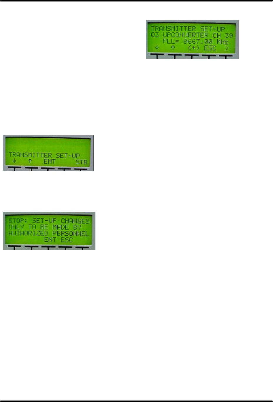
UHF Analog Driver/Transmitter/ Chapter 5, Detailed Alignment Procedures
Translator
LX Series, Rev. 3 5-5
5.4 Changing the Transmitter
Channel Procedure
NOTE: Depending on the new channel
frequency, the bandpass filter may need
to be retuned or replaced to achieve
maximum output power.
Place the transmitter in Standby and go
to the Set Up Menu, Transmitter
Configuration Access Screen, on the LCD
Display by pushing the down arrow on
the default main screen and each
succeeding screen until the Transmitter
Set-Up Main Screen appears.
Transmitter Set-Up, Configuration
Access Screen
Enter the Set-Up screens by pushing the
ENT button. The following screen will
appear.
Authorized Personnel Screen
This screen of the transmitter notifies an
operator that they are only to proceed if
they are authorized to make changes to
the transmitter's operation. This screen
is implemented in transmitter software
version 1.4 and above. Push the ENT
button and step through the Set Up
screens by pushing the Down Arrow
button until the screen labeled
“Upconverter CH xx” is reached, as
shown below. The example below
shows the Transmitter set to Channel
39.
Transmitter Set-up: Upconverter
Channel Select Screen
The choices of this screen are to the
standard UHF/VHF channels. The
channel number should be blinking. To
change the channel, hit the + button to
step through the channels until the
desired channel is reached.
To select a 10kHz offset to the channel
frequency, use the > button to move
the curser to the LO frequency listed
below the Channel number, and keep
pressing the > button until the desired
digit is blinking, and then use the +
button to change the frequency.
Example:
Nominal LO frequency for Channel 39 =
0667.00 MHz. To generate a + offset,
change the LO frequency to 0667.01
MHz. To generate a – offset, change the
LO frequency to 0666.99 MHz.
A safeguard is added to the Set Up
Menus in software version 2.5 and
above. If a change is made to a screen
within the Set Up Menu, as was just
completed with the channel change,
when you go to the next menu, by
pushing the Down or Up Arrow, a screen
appears that asks if you accept the
change or want to return to the previous
menu to reconsider the changes made.
See the Accept or Return to previous
Menu Screen. To accept the changes,
the two buttons located under ACCEPT
must be pushed simultaneously. To
return to the previous Menu to make
corrections, the two buttons located
under the RETURN must be pushed
simultaneously. Upon returning to the
previous Menu the correct input must be
entered and the above procedure
repeated, this time accepting the
changes.
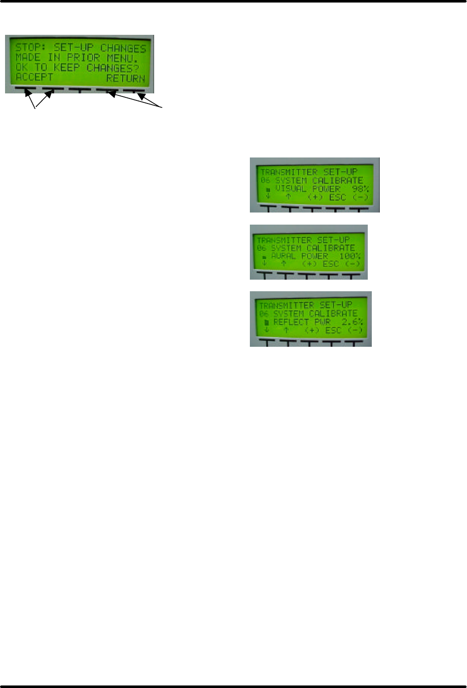
UHF Analog Driver/Transmitter/ Chapter 5, Detailed Alignment Procedures
Translator
LX Series, Rev. 3 5-6
Accept or Return to previous Menu
Screen
Pushing these two Pushing these
buttons together two buttons
will accept the together will return
change. you to the previous
Menu.
Accepting the changes will put you back
to the Main Set-Up Screen.
5.5 Calibration of Output and
Reflected Power for transmitters up
to 100W
NOTE: Only perform the following
procedures if the output power
calibration is suspect.
NOTE: If your transmitter is higher than
100W with external Power Amplifiers
then proceed to Sections 5.6 & 5.7.
5.5.1 Calibration of Output Power
for transmitters up to 100W
Switch the transmitter to Standby and
place the Upconverter into Manual Gain.
Preset R205, the aural null pot on the
Amp Control board, fully CCW. Adjust
R204, the null offset pot on the Amp
Control board, for 0% visual output.
Perform the following adjustments with
no aural present by removing the aural
IF carrier jumper on the back of the
chassis assembly. Connect a sync and
black test signal to the video input jack
of the test modulator. Switch the
transmitter to Operate.
Next, set up the transmitter for the
appropriate average output power level:
Example is for a 100 Watt Transmitter.
• Sync + black 0 IRE
setup/wattmeter=59.5 watts
• Sync + black 7.5 IRE
setup/wattmeter=54.5 watts
NOTE: The transmitter must have 40 IRE
units of sync.
Adjust R202, visual calibration, on the
Amp Control board for 100% on the front
panel LCD display in the % Visual Output
position. (Examples of the screens are
shown below).
With the spectrum analyzer set to zero
span mode, obtain a peak reference on
the screen. Reconnect the aural carrier
jumper on the rear of the chassis
assembly. Turn the power adjust pot on
the front panel until the original peak
reference level is attained. Adjust R203
for a 100% aural power reading. Switch
to the Visual Output Power position and
adjust R205 (aural null pot) for 100%
visual power.
5.5.2 Calibration of Reflected Power
for transmitters up to 100W
To calibrate the reflected output power
reading of the transmitter. Reduce the
manual gain pot R3 to a 10% reading on
the LCD front panel display in the %
Output Power position. Place the
transmitter in Standby. Remove the PA
Module Sled. Remove the load from J4
on the (A4) Directional Coupler Board
and switch the LCD Display screen to the
Reflected Output Power position.

UHF Analog Driver/Transmitter/ Chapter 5, Detailed Alignment Procedures
Translator
LX Series, Rev. 3 5-7
Reinstall the PA Module. Switch the
transmitter to operate. Adjust the
reflected power calibration adjust pot
R163 on the power amplifier module to a
10% reading. A reflected power fault
should be present on the LCD Display.
Reconnect the load to J4 in the module.
After this calibration is completed, move
switch SW1 on the upconverter module
to the Automatic AGC position. This is
the normal operating position for the
switch. Adjust the ALC pot on the IF
Processor is needed to attain 100%
output power. Switch to Manual Gain
(Manual AGC) and adjust the Manual
Gain pot for 100 % output power.
Switch the upconverter back to
Automatic AGC.
5.6 Adjusting the IF ALC Gain, the
AGC 1, AGC 2, and the Overdrive
Cutback Protection (AGC Cutback) in
Transmitters with Output Power
above 100 Watts
NOTE: Only perform the following
procedure on transmitters above 100W
with external Power Amplifiers present.
Before beginning this procedure, put the
transmitter into standby and preset the
following pots and switches. Put the
Man/Auto ALC switch in the Man mode,
turn the ALC Manual Gain Pot and ALC
mode Pot, on the IF processor, full
counter clockwise, also put the
Man/Auto AGC switch in the Man mode
and turn the AGC Man Gain pot and AGC
Adj pot on the upconverter module full
counter clockwise. Set the AGC cut-in
Adj pot full clockwise. Now you can re-
enable the transmitter and begin the
following procedure.
The ALC switch should already be in the
Manual mode. Adjust the ALC Man Gain
pot, located on the front panel of the IF
Processor module, to 0.8 volts. Next,
set the IF ALC to the Auto mode. Turn
the ALC Adj. pot, located on the front of
the IF Processor, clockwise until the ALC
is at 0.8 volts, which stays constant to
control the loop around the correction.
AGC1 is at RF and controls the loop to
the output of the driver. The AGC
switch on the front of the Upconverter
should be in the Manual mode. Turn the
AGC Man Gain pot clockwise until the
output of the transmitter is at full
power. Calibrate the output metering on
the driver to 100%. AGC1 should be at
.8 volts with the Driver at 100% output.
With the AGC still in the manual mode
and the transmitter at full power,
calibrate the Transmitter output metering
to 100%. In transmitters that utilize
external amplifier modules and with the
transmitter at full power and 100% O/P
metering, the Forward Power readings for
each of the amplifier modules should be
readjusted to a 100% Forward Power
reading. NOTE: The transmitter AGC
must be in the Manual Gain position
when readjusting the module forward
power. These amplifier readings can be
found under the Transmitter Details Main
Screen, by arrowing down to each Amp
Set and each Module in turn.
Set the Man/Auto AGC Switch, located on
the front of the Upconverter, to Auto and
readjust the transmitter output power
level to 100% with the AGC Adj pot. The
external amplifiers should have all been
set up for 100% Forward Power readings
previously and should return to 100%
after setting the transmitter output level
to 100% in the Auto mode.
Next, the Inner Loop Gain is adjusted
until the power starts to decrease, this
means that AGC1 and AGC2 are at the
same voltage. When at the cut-in point,
look on the display at the gain value of
the inner loop (0 to 255). Whatever the
value is, decrease the inner loop gain
level by 10%. (Example, if the display
shows 200, decrease to 180). This sets
the difference between AGC1 and AGC2.
There is no adjustment for AGC2,
therefore AGC2 is what it is, but should
be around 0.9 Volts.
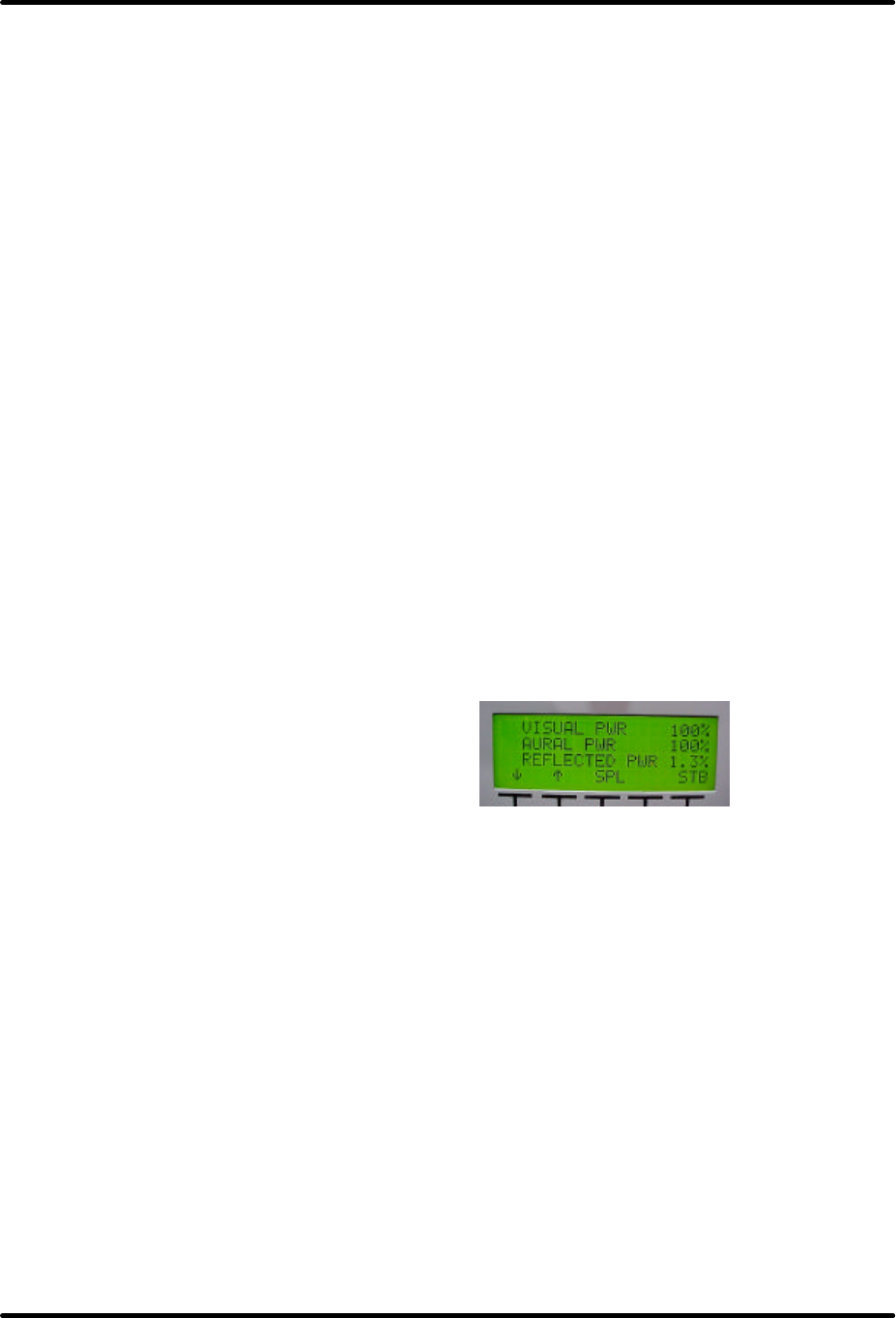
UHF Analog Driver/Transmitter/ Chapter 5, Detailed Alignment Procedures
Translator
LX Series, Rev. 3 5-8
Overdrive Protection Setup (AGC
Cutback): Adjust the output power to
110%, 10% above 100%. Next, setup
the overdrive cut-in by adjusting the
AGC Cutback Pot. Slowly turn the AGC
Cutback Pot, located on the front of the
upconverter, Counterclockwise until
the AGC Override light begins to flicker,
and the output power begins to drop.
Turn the pot Clockwise slightly, so the
light just goes out and the power
stabilizes. Repeat if needed. Re-adjust
the AGC ADJ pot as needed until the
power level returns to the 100% output
power level.
The Transmitter is ready for normal
operation.
5.7 Calibration of Output and
Reflected Power for transmitters
above 100W with external Power
Amplifiers
NOTE: If your transmitter is 100W or
less in power, then use the Section 5.5
calibration procedure to recalibrate the
system.
NOTE: Only perform the following
procedures if the output power
calibration is suspect.
5.7.1 Calibration of the Transmitter
Forward Output Power Level for
transmitters with external Power
Amplifiers
Switch the transmitter to Standby and
preset R51, the aural null pot on (A4) the
visual/aural metering board, fully CCW.
Switch the Upconverter sled to Manual
Gain. Adjust R48, the null offset pot on
the visual/aural metering board, full CW.
Adjust CCW until 0% visual output is
displayed on the LCD Display in the
System Visual Power position. Perform
the following adjustments with no aural
present by removing the jumper cable,
the aural IF loop-through, that is
connected on the rear of the
exciter/driver chassis. Connect a sync
and black test signal to the video input
jack of the exciter/driver. Switch the
transmitter to Operate.
Next, set up the transmitter for the
appropriate average output power level
using the Manual Gain pot on the
Upconverter sled:
Example is for a 1000 Watt transmitter.
• Sync + black 0 IRE
setup/wattmeter=595 watts
• Sync + black 7.5 IRE
setup/wattmeter=545 watts
NOTE: The transmitter must have 40 IRE
units of sync.
Adjust R28, visual calibration, on the
(A4) visual/aural metering board for .8V,
at TB30-14 and TB30-12 return, on the
exciter/driver assembly, then adjust
display to read 100% on the front panel
meter in the System Forward Power
position. (Example of screen shown
below).
With the spectrum analyzer set to zero
span mode, obtain a peak reference on
the screen. Reconnect jumper cable on
the rear of the exciter/driver. While in
the Visual Output Power position, adjust
L3 for a minimum visual power reading
on the LCD display. Turn the power
adjust pot on the Upconverter sled front
panel until the original peak reference
level is attained. Peak L1 and C8 for a
maximum aural power reading, then
adjust R20 for .8V, at TB30-15 and
TB30-12 return, on the exciter/driver
assembly, then adjust LCD display for
100% system aural power reading.
Switch to the Visual Output Power
position and adjust R51 for 100% visual
power on system LCD display. Switch
the Upconverter to Auto and adjust the

UHF Analog Driver/Transmitter/ Chapter 5, Detailed Alignment Procedures
Translator
LX Series, Rev. 3 5-9
IF ALC Gain Pot for 100% Output.
(Example of screen shown above).
5.7.2 Calibration of the Transmitter
Reflected Output Level for
transmitters with external Power
Amplifiers
On the meter, in the Visual Power
position, turn the power adjust pot to
10%. Move the Reflected cable on the
(A11) coupler to the unused “INC” port
on the coupler. Then adjust R39 on (A4)
the visual/aural metering board for a
.32VDC, at TB30-13 and TB30-12 return,
on the exciter/driver assembly. Next,
adjust the LED display for 10% reading in
the System Reflected Power position. At
this 10% reference power reading a
reflected power fault should appear on
the System Errors Menu. The Fault is
adjustable in the Set-Up Menu. Turn the
power adjust pot slightly CCW and the
fault should be clearable on the System
Error Menu. Turn the pot CW until the
Fault appears. The reflected output
power is now calibrated. Switch the
transmitter to Standby and move the
Reflected power cable on the A11
Coupler back to the “Reflected Port”.
5.8 Linearity Correction Adjustment
As shipped, the exciter was preset to
include amplitude and phase pre-
distortion. The pre-distortion was
adjusted to approximately compensate
the corresponding non-linear distortions
of the Power Amplifier.
NOTE: On the IF processor board inside
the module the correction enable/disable
jumper W12 on J30 must be in the
Enable position, on pins 2 & 3. This is
the normal operating position.
Set up a spectrum analyzer with
100 kHz resolution bandwidth and
100 kHz video bandwidth to monitor the
intermodulation products of the RF
output signal of the Power Amplifier.
A typical red field spectrum is shown in
Figure 5-1. There are three Linearity
Corrector stage adjustments located on
the front panel of the IF Processor
Module. The adjustments are threshold
settings that are adjusted as needed to
correct for any amplitude or phase
intermod problems. Adjust the top
linearity correction adjustment R211
threshold cut in for the in phase
amplitude distortion pre-correction that
is needed. Next adjust the middle
linearity correction adjustment R216
threshold cut in also for the in phase
amplitude distortion pre-correction that
is needed. Finally adjust the bottom
linearity correction adjustment R231
threshold cut in for the quadrature
phase distortion pre-correction that is
needed. The above pots are adjusted
for the greatest separation between the
peak visual carrier and the intermod
products. NOTE: These pots affect
many other video parameters, so care
should be taken when adjusting the
linearity correction.
Figure 5-1. Typical Red Field Spectrum

UHF Analog Driver/Transmitter/ Chapter 5, Detailed Alignment Procedures
Translator
LX Series, Rev. 3 5-10
5.9 Frequency Response Delay
Equalization Adjustment
NOTE: Perform the following procedure
only if a frequency response delay
equalization problem is suspect.
The procedure for performing a
frequency response delay equalization
adjustment for the transmitter is done at
IF and is described in the following steps:
The center frequency for the first stage is
45 MHz. Adjust R103, the top frequency
response equalizer pot, located on the
front panel of the IF Processor Module,
for the best depth of frequency response
correction at 45 MHz.
The center frequency for the second
stage is 42 MHz. Adjust R106, the
middle frequency response equalizer pot,
located on the front panel of the IF
Processor Module, for the best depth of
frequency response correction at 42 MHz.
The center frequency for the second
stage is 43.5 MHz. Adjust R274, the
bottom frequency response equalizer pot,
located on the front panel of the IF
Processor Module, for the best depth of
frequency response correction at 43.5
MHz.
After the three delay attenuation
equalizers have been adjusted, fine tune,
as needed, for the best frequency
response across the channel.
5.10 (A9) Bandpass Filter Assembly
NOTE: If your system contains a
Teracom manufactured tunable filter
assembly, refer to the manufacturers
manual included with the filter for
instructions on tuning and ignore the
following sections on the Axcera
manufactured Bandpass and Trap Filter
Assemblies.
NOTE: The bandpass filter and the
(optional) trap filter are factory swept to
the proper channel and should not be
tuned without the proper equipment. Do
not attempt to tune the filters without a
sweep generator or, preferably, a
network analyzer. If tuning is thought to
be required, consult with the Axcera Field
Support Department before attempting
to tune the filters.
The bandpass filter is made of aluminum
waveguide and has five resonant cavities.
The filter has five bolts for tuning
adjustments, three located in the middle
on the left and two on the right, and four
or six rods on the front of the bandpass
filter, depending upon the channel, for
coupling adjustments between the
sections. The bandpass filter also utilizes
two integral traps at -4.5 MHz and +9
MHz from FV at the top and bottom,
respectively, of the left-hand side of the
bandpass filter, looking from the rear of
the cabinet. Figure 5-2 shows the
location of the bolts used for making
tuning adjustments.
To tune the filter, connect a sweep signal
to the input of the filter and adjust the
five tuning bolts for a 6-MHz bandwidth
and a flat-frequency response across the
desired band.
NOTE: The bandpass ripple should be
≤0.25 dB. The 6-MHz band should also
have a minimum of 20 dB return loss
across the pass band.
See Table 5-1 for typical bandpass
values.
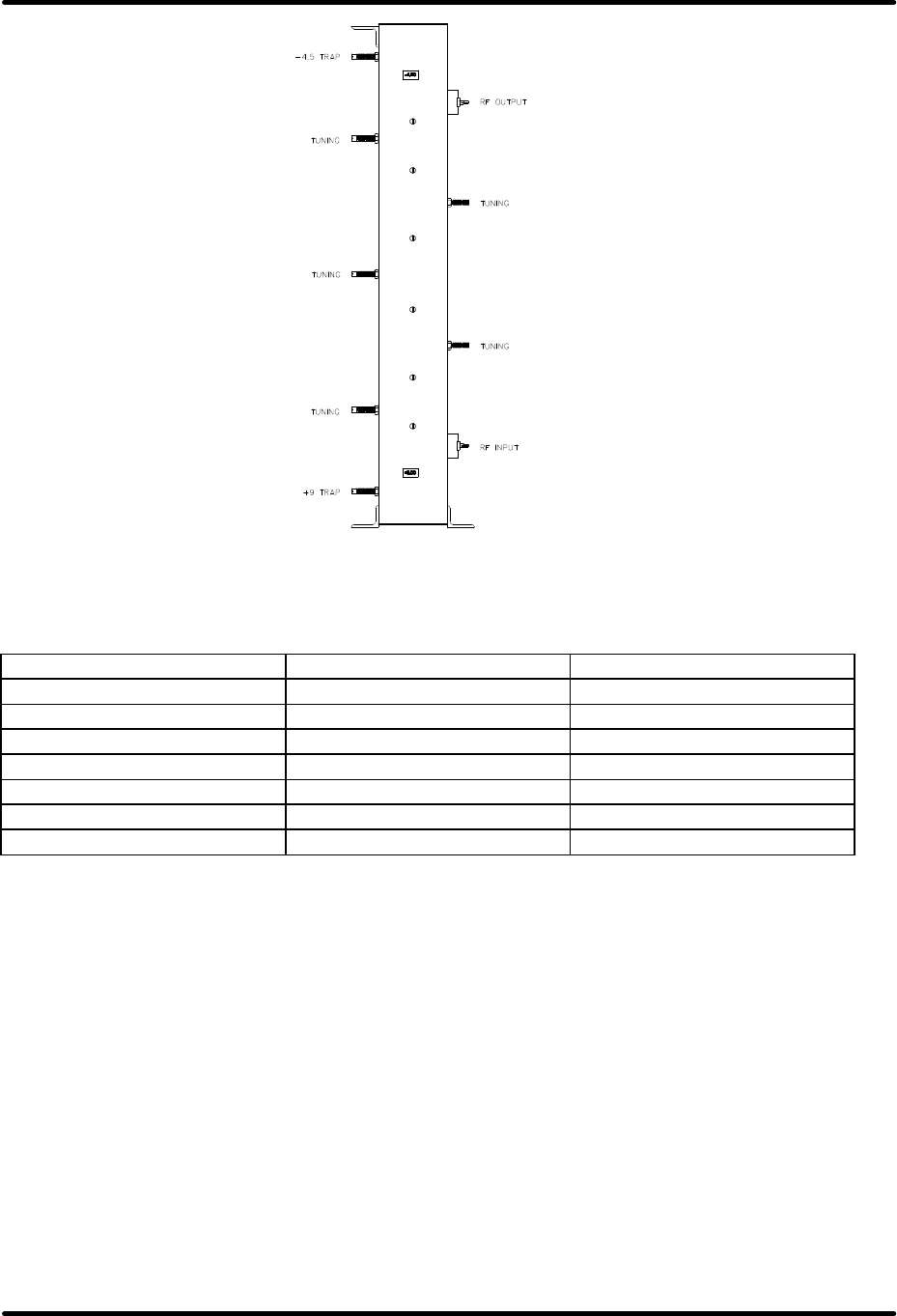
UHF Analog Driver/Transmitter/ Chapter 5, Detailed Alignment Procedures
Translator
LX Series, Rev. 3 5-11
Figure 5-2. Bandpass Filter
Table 5-1. Typical Bandpass Values
FREQUENCY INSERTION LOSS (dB) RETURN LOSS (dB)
FV-4.5 ≥ 35
FV-0.5 ≥ 20
FV ≤ 0.6 ≥ 20
Fa ≤ 0.6 ≥ 20
FV+8.08 ≥ 15
FV-9 ≥ 30
2FV ≥ 30
5.11 (A10) UHF Trap Filter Assembly
The Traps on the output Trap Filter are
labeled with their Center Frequency
relative to the Frequency of the Carrier.
(For Example: The Traps labeled -4.5
MHz are tuned for a Center Frequency of
4.5 MHz Lower than the Frequency of
the Visual Carrier.) The first section of
the Trap Filter filters out the Visual
Carrier plus 9 MHz (fv+9 MHz). The
second and fourth sections work
together to filter out the lower spurious
product (fv-4.5 MHz). The third section
is tuned to remove the (fv+8.08). The
output of the Trap Filter is an "N" Type
Connector. The Trap Sections have
been factory tuned and should not need
major adjustments. The Trap Filter is
comprised of four trap sections
connected to the main transmission line.
The Trap Sections are Reflective
Notches, adjustable across the entire
UHF Frequency Band. The electrical
length of the Outer Sleeve and the
Center Rod of the Notch can be adjusted
to Tune the Notch Frequency. The
Depth of the Notch is set by the gap
between the Center Conductor of the
Trap Section and the Center Conductor
of the Main Line. Tight Coupling makes

UHF Analog Driver/Transmitter/ Chapter 5, Detailed Alignment Procedures
Translator
LX Series, Rev. 3 5-12
a Deep Notch, while Loose Coupling
makes a Shallow Notch.
FINE TUNING of the Notches Center
Frequency can be accomplished with the
Tuning Bolts located on the side of the
Filter Section. Loosen the nut locking the
Bolt in place and adjust the Bolt to
change the Frequency of the Notch.
Monitor the output of the Transmitter
with a Spectrum Analyzer and Null the
Distortion Product with the Bolt. Red
Field is a good Video Test Signal to use to
see the +8.08 MHz Product. Tighten the
nut when the tuning is completed. Hold
the bolt in place with a screwdriver as
the nut is tightened to prevent it from
slipping.
MAJOR TUNING, such as changing the
Notch Depth or moving the Notch
Frequency more than 1 MHz, the Outer
Conductor and the Center Conductor of
the Trap Section must both be moved.
This requires a RF Sweep Generator to
accomplish. Apply the Sweep signal to
the Input of the Trap Filter and monitor
the Output. Loosen the Clamp holding
the Outer Conductor in place and make
the length longer to Lower the frequency
of the Notch or shorter to Raise the
frequency of the Notch. Loosen the
Center Conductor with an Allen Wrench
and move it Deeper for a Lower
Frequency Notch or out for a Higher
Frequency Notch. These adjustments
must both be made to change the Notch
Frequency. Moving only the Center
Conductor or the Outer Conductor will
affect the Notch Depth in addition to the
Center Frequency. The variable that is
being adjusted with this procedure is the
length of the Center Conductor inside the
Trap Filter. The gap between the Trap
and the Main Line should not be changed.
Moving only the Inner or the Outer
Conductors by itself will affect the Gap
and the Notch depth. To affect the Notch
Depth Only, both sections will have to be
moved. The Notch Depth is controlled by
the Gap between the Center Conductor
and the Trap Section. This Gap also has
an effect on the Center Frequency. To
Deepen the Notch, Shorten the Outer
Conductor and pull the Center Conductor
Out until the Notch is back in the same
place. Move the Sections in the opposite
direction to make a Shallow Notch.
NOTE: The Trap Filter is typically
adjusted for a notch depth of 10 dB.
5.11.1 The Effects of Tuning the
Output Trap Filter
Lengthening Outer Conductor Only -
Notch Frequency Up, Shallower Notch.
Shortening Outer Conductor Only -
Notch Frequency Down, Deeper Notch.
Inserting Inner Conductor Deeper -
Notch Frequency Down, Deeper Notch.
Inserting Less Inner Conductor -
Notch Frequency Up, Shallower Notch.
Tuning Bolt In - Notch Frequency
Down.
Tuning Bolt Out - Notch Frequency Up.
Moving both Inner and Outer
Conductors to keep the Same Gap
inside - Center Frequency Moves, Notch
Stays the Same.
After tuning has been completed, tighten
the Clamp and the Allen Screws that hold
the Conductors. Use the Fine Tuning
Bolts to bring the Frequency In. The
Final Tuning Adjustments should be
completed with the Transmitter driving
the Output Trap Filter for at least one
hour to allow for warm-up drift.
The Transmitter is ready for normal
operation.
NOTE: In Dual Exciter Systems, with an
exciter switcher, repeat the above
procedure with Exciter B selected as the
On Air Exciter. The exciter switcher
must be in manual.

UHF Analog Driver/Transmitter/ Chapter 5, Detailed Alignment Procedures
Translator
LX Series, Rev. 3 5-13
This completes the detailed alignment
procedures for the LX Series transmitter.
If a problem occurred during the
alignment, help is available by calling
Axcera field support at (724) 873-8100.
APPENDIX A
LX SERIES ANALOG
SYSTEM SPECIFICATIONS
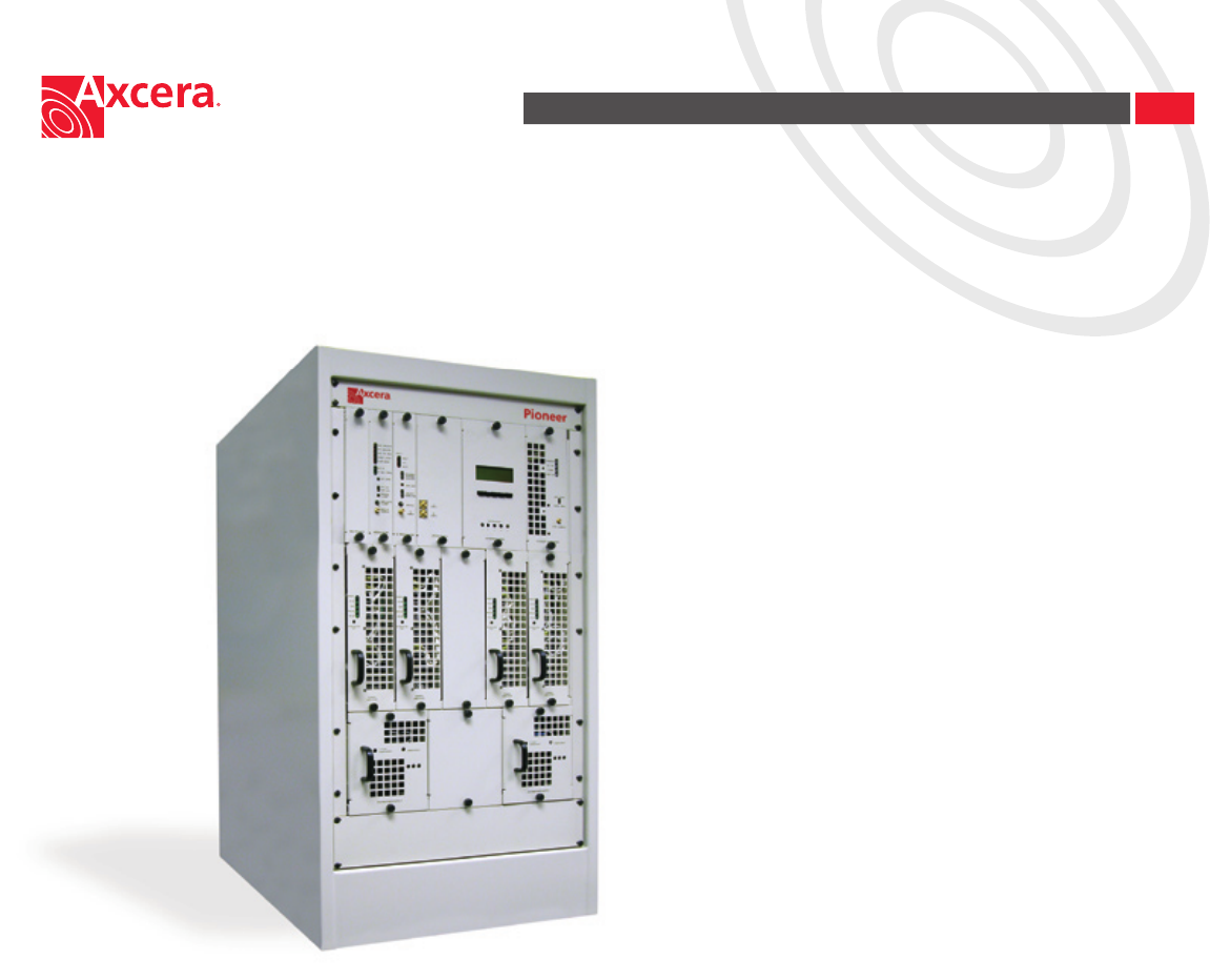
Pioneer (Preliminary)
Low Power Transmitter 10W-2kW
Designed to provide broadcasters with a product that will meet their needs like
no other solution on the market, this new low to medium power transmitter
line uses the latest devices for broadband operation across each band. This
allows users to minimize spare parts stock, which is especially important to
group owners and networks, and also enables simple and inexpensive channel
changes.
The very compact and completely modular design uses a chassis/backplane
conguration with parallel amplier and power supply modules which can be
removed and replaced while the transmitter is on the air. Additionally, the Pioneer
series was designed to be eld upgradable to digital operation.
Congurations are available in power levels from 10 watts to 2 kilowatts
analog and up to 1 kilowatt DTV, and all are manufactured in the USA by
Axcera - The RF Experts.

Speci cations published here are current as of the date of publication of this document. Because we are continuously improving our products, Axcera reserves the right to
change speci cations without prior notice. At any time, you may verify product speci cations by contacting our of ce. Axcera views it’s patent portfolio as an important
corporate asset and vigorously enforces its patents. Products or features contained herein may be covered by one or more U.S. or foreign patents.
0308R2 © 2003 AXCERA All Rights Reserved An Equal Opportunity Employer A Platinum Equity Company
Visual Performance
Frequency Range 470 to 806 MHz
Carrier Stability (Transmitters)
Standard ±1 kHz
Optional ±350 Hz
w/PFC ±1Hz
Frequency Translation Stability (Translators)
Standard ±1 kHz
Optional ±350 Hz
w/PFC ±1Hz
Regulation of RF Output Power 3%
Output Variation (Over 1 Frame) 2%
Sideband Response
-1.25 MHz and below -20 dB
-0.75 to -0.5 MHz +0.5 db, -2 dB
-0.5 to +3.58 MHz ±0.5 dB
+3.58 MHz to +4.18 MHz +0.5, -1.0 dB
Freq Response vs. Brightness ±0.5 dB
Visual Modulation Capability 1%
Differential Gain 5%
Incidental Phase Modulation ±3°
Linearity (Low Frequency) 5%
Aural Performance
Frequency Deviation Capability ±75 kHz
(Transmitters)
Distortion 0.5%
FM Noise -60 dB
AM Noise -55 dB
Aural to Visual Separation 4.5 MHz
± 100Hz
Composite Audio Input (Multi-channel sound)
(Transmitters)
Input Level 1V peak,
nominal
Input Impedance 75 ohms,
unbalanced
Frequency Range
±0.1 dB response 50 Hz to 50 kHz
±0.5 dB response 30 Hz to 120 kHz
Monaural Audio Input (Transmitters)
Input Level 0 to +10 dBm
Input 600 ohms,
balanced
Freq Range (±0.5 dB resp.) 30 Hz to 15 kHz
Pre-emphasis 75µs
Subcarrier Input (Transmitters)
Input Level 1V peak,
nominal
Input Impedance 75 ohms,
unbalanced
Freq Range (±0.5 dB resp.) 20 kHz to
120 kHz
Pioneer (Preliminary)
Low Power Transmitter 10W - 2kW
Visual Performance (continued)
Differential Phase ±3°
Signal-to-Noise Ratio 55 dB
2t K-Factor 2%
Noise Factor (Translators) 5 dB (Max)
w/Input Preamp 3 dB (Max)
Input Dynamic Range (Translators) -60 dB to
-15 dBm
w/Input Preamp -75 dBm
to -30 dBm
Env. Delay (Transmitters) Per FCC Standard
Video Input (Transmitters) 75 ohms
(Loop through)
Harmonics -60 dB or better
Intermodulation Products -52 dB or better
Spurious (›3 MHz from channel edge)
100W and lower -50dB or better
Greater than 100W -60dB or better
General
Model Number* LU10Ax LU100Ax LU250Ax LU500Ax LU1000Ax LU2000Ax
Power Output (Watts)
Visual (Peak) 10 100 250 500 1000 2000
Aural (Avg.) 1 10 15 50 100 200
Output Connector N N 7/8” EIA 7/8” EIA 7/8” EIA 7/8” EIA
Power Consumption (Watts) 250 675 1100 1900 3500 6700
Input Power
Line Voltage (Volts) 117/230 ±10% 230 ± 10%
Power Requirements Single Phase, 50 or 60 Hz
Size (H x W x D) 8.75”x19”x23” 55”x22”x34”
(Chassis Only)
Weight (lbs.) 45 45 340 360 400 550
Operational Temperature Range 0 to +50°, derate 2°C/1000 ft.
Maximum Altitude3 8500 feet (2600m) AMSL
Operational Humidity Range 0% to 95% non-condensing
RF Load Impedance 50 Ω
* For transmitters use “T” suf x, translators use “L” suf x (ex. LU100AT - 100W Transmitter)
APPENDIX B
DRAWINGS LIST

UHF Analog Driver/Transmitter/Translator Appendix B, Drawings and Parts Lists
LX Series, Rev. 3 B-1
Innovator LX Series Analog System
LX Series 10W to 100W System Block Diagram ......................................1302139
LX Series Analog Transmitter/Translator System Interconnect..................1307260
Chassis Assembly, 110/220 VAC Exciter, V2, LX Series
Interconnect.......................................................................................1304064
Backplane Board, V2, LX Series
Schematic..........................................................................................1304049
Modulator Assembly, M/N (May not present in Translator Systems)
Analog Modulator Board, System M/N
Schematic..........................................................................................1301798
Receiver Assembly, UHF (Part of Translator System)
Interconnect.......................................................................................1304005
Block Diagram....................................................................................1304004
IF ALC Board, UHF Receiver Assembly 1304002)
Schematic..........................................................................................1304011
UHF Mixer/PLL Board, (Used in UHF Receiver Assembly 1304002)
Schematic..........................................................................................1304023
UHF Preamplifier Board, (Used in UHF Receiver Assembly 1304002)
Schematic..........................................................................................1304091
IF Processor Assembly
IF Processor Board
Schematic..........................................................................................1301983
VHF/UHF Upconverter Assembly
Block Diagram....................................................................................1303830
Interconnect.......................................................................................1303831
Downconverter Board Assembly
Schematic..........................................................................................1303836
First Conversion Board, LX Series
Schematic..........................................................................................1303840
L-Band PLL Board, LX Series
Schematic..........................................................................................1303848
Upconverter Control Board, LX Series
Schematic..........................................................................................1304761
Control/Power Supply Assembly, 110 /220 VAC
Block Diagram....................................................................................1303889
Interconnect.......................................................................................1302062
Control Board
Schematic..........................................................................................1302023

UHF Analog Driver/Transmitter/Translator Appendix B, Drawings and Parts Lists
LX Series, Rev. 3 B-2
Power Protection Board
Schematic..........................................................................................1302839
Switch Board
Schematic.......................................................................................1527-3406
Power Amplifier Assembly
Block Diagram....................................................................................1303850
Interconnect.......................................................................................1303814
Driver Power Amplifier Assembly
Block Diagram....................................................................................1305138
Interconnect.......................................................................................1305137
UHF Filter, (Used in PA Assembly 1307184)
Schematic.......................................................................................1007-3101
Coupler Board Assembly
Schematic..........................................................................................1303152
Amplifier Control Board
Schematic..........................................................................................1303683
1 Watt Module Assembly
Schematic..........................................................................................1302762
RF Module Pallet, Philips
Schematic........................................................................51-5379-309-00 WSP
APPENDIX C
TRANSMITTER LOG SHEET
UHF LX Series Driver/Transmitter/Translator Appendix C, Log Sheet
- Page 1 of 1 -
DESCRIPTION OF
PARAMETER TRANSMITTER READING FROM LCD DISPLAY
DATE READINGS TAKEN
Model Number
Code Version
Firmware Number
OUTPUT MEASUREMENTS
% VISUAL POWER
% AURAL POWER
RECEIVER DETAILS NOT USED WITH TRANSMITTER
AFC 1 LEVEL
PLL 1 CIRCUIT
ALC INPUT
FAULT AT
MODULATOR DETAILS MAY NOT BE USED WITH TRANSLATOR
PLL CIRCUIT
OUTPUT LEVEL
AURAL DEVIATION
CW INPUT
CALL SIGN
IF PROCESSOR DETAILS
INPUT SIGNAL STATE
MODULATION
INPUT IF
DLC CONTROL LOCK
ALC LEVEL
ALC MODE
UPCONVERTER DETAILS
AFC 1 LEVEL
AFC 2 LEVEL
CODE VERSION
PLL 1 CIRCUIT
PLL 2 CIRCUIT
AGC 1 LEVEL
AGC 2 LEVEL
INT. 10 MHz
SYSTEM CONTROL DETAILS
Power Supply Enable For
UHF LX Series Driver/Transmitter/Translator Appendix C, Log Sheet
- Page 2 of 2 -
DESCRIPTION OF
PARAMETER TRANSMITTER READING FROM LCD DISPLAY
DRIVER AND PA DETAILS
POWER SUPPLY STATE, 32V
FORWARD POWER
REFLECTED POWER
AMP 1 CURRENT
AMP 2 CURRENT
TEMPERATURE
CODE VERSION
PA HAS OPERATED FOR
EXT. PA AMPLIFIER MODULES ONLY IN HIGH POWER SYSTEMS
AMP SET 1 MODULE 1 Will indicate Amp Set and Module within the
Set. Will step through each Set and Module.
POWER SUPPLY VOLTAGE, 32V
32V SUPPLY
FORWARD POWER
REFLECTED POWER
AMP CURRENT 1
AMP CURRENT 2
AMP CURRENT 3
AMP TEMPERATURE
CODE VERSION
PA HAS OPERATED FOR
AMP SET 1 MODULE 2
POWER SUPPLY VOLTAGE, 32V
32V SUPPLY
FORWARD POWER
REFLECTED POWER
AMP CURRENT 1
AMP CURRENT 2
AMP CURRENT 3
AMP TEMPERATURE
CODE VERSION
PA HAS OPERATED FOR
AMP SET 1 MODULE 3
POWER SUPPLY VOLTAGE, 32V
32V SUPPLY
FORWARD POWER
REFLECTED POWER
AMP CURRENT 1
AMP CURRENT 2
AMP CURRENT 3
AMP TEMPERATURE
CODE VERSION
PA HAS OPERATED FOR

UHF LX Series Driver/Transmitter/Translator Appendix C, Log Sheet
- Page 3 of 3 -
DESCRIPTION OF
PARAMETER TRANSMITTER READING FROM LCD DISPLAY
AMP SET 1 MODULE 4
POWER SUPPLY VOLTAGE, 32V
32V SUPPLY
FORWARD POWER
REFLECTED POWER
AMP CURRENT 1
AMP CURRENT 2
AMP CURRENT 3
AMP TEMPERATURE
CODE VERSION
PA HAS OPERATED FOR
AMP SET 2 MODULE 1
POWER SUPPLY VOLTAGE, 32V
32V SUPPLY
FORWARD POWER
REFLECTED POWER
AMP CURRENT 1
AMP CURRENT 2
AMP CURRENT 3
AMP TEMPERATURE
CODE VERSION
PA HAS OPERATED FOR
AMP SET 2 MODULE 2
POWER SUPPLY VOLTAGE, 32V
32V SUPPLY
FORWARD POWER
REFLECTED POWER
AMP CURRENT 1
AMP CURRENT 2
AMP CURRENT 3
AMP TEMPERATURE
CODE VERSION
PA HAS OPERATED FOR
AMP SET 2 MODULE 3
POWER SUPPLY VOLTAGE, 32V
32V SUPPLY
FORWARD POWER
REFLECTED POWER
AMP CURRENT 1
AMP CURRENT 2
AMP CURRENT 3
AMP TEMPERATURE
CODE VERSION
PA HAS OPERATED FOR

UHF LX Series Driver/Transmitter/Translator Appendix C, Log Sheet
- Page 4 of 4 -
DESCRIPTION OF
PARAMETER TRANSMITTER READING FROM LCD DISPLAY
AMP SET 2 MODULE 4
POWER SUPPLY VOLTAGE, 32V
32V SUPPLY
FORWARD POWER
REFLECTED POWER
AMP CURRENT 1
AMP CURRENT 2
AMP CURRENT 3
AMP TEMPERATURE
CODE VERSION
PA HAS OPERATED FOR
AMP SET 3 MODULE 1
POWER SUPPLY VOLTAGE, 32V
32V SUPPLY
FORWARD POWER
REFLECTED POWER
AMP CURRENT 1
AMP CURRENT 2
AMP CURRENT 3
AMP TEMPERATURE
CODE VERSION
PA HAS OPERATED FOR
AMP SET 3 MODULE 2
POWER SUPPLY VOLTAGE, 32V
32V SUPPLY
FORWARD POWER
REFLECTED POWER
AMP CURRENT 1
AMP CURRENT 2
AMP CURRENT 3
AMP TEMPERATURE
CODE VERSION
PA HAS OPERATED FOR
AMP SET 3 MODULE 3
POWER SUPPLY VOLTAGE, 32V
32V SUPPLY
FORWARD POWER
REFLECTED POWER
AMP CURRENT 1
AMP CURRENT 2
AMP CURRENT 3
AMP TEMPERATURE
CODE VERSION
PA HAS OPERATED FOR

UHF LX Series Driver/Transmitter/Translator Appendix C, Log Sheet
- Page 5 of 5 -
DESCRIPTION OF
PARAMETER TRANSMITTER READING FROM LCD DISPLAY
AMP SET 3 MODULE 4
POWER SUPPLY VOLTAGE, 32V
32V SUPPLY
FORWARD POWER
REFLECTED POWER
AMP CURRENT 1
AMP CURRENT 2
AMP CURRENT 3
AMP TEMPERATURE
CODE VERSION
PA HAS OPERATED FOR
AMP SET 4 MODULE 1
POWER SUPPLY VOLTAGE, 32V
32V SUPPLY
FORWARD POWER
REFLECTED POWER
AMP CURRENT 1
AMP CURRENT 2
AMP CURRENT 3
AMP TEMPERATURE
CODE VERSION
PA HAS OPERATED FOR
AMP SET 4 MODULE 2
POWER SUPPLY VOLTAGE, 32V
32V SUPPLY
FORWARD POWER
REFLECTED POWER
AMP CURRENT 1
AMP CURRENT 2
AMP CURRENT 3
AMP TEMPERATURE
CODE VERSION
PA HAS OPERATED FOR
AMP SET 4 MODULE 3
POWER SUPPLY VOLTAGE, 32V
32V SUPPLY
FORWARD POWER
REFLECTED POWER
AMP CURRENT 1
AMP CURRENT 2
AMP CURRENT 3
AMP TEMPERATURE
CODE VERSION
PA HAS OPERATED FOR

UHF LX Series Driver/Transmitter/Translator Appendix C, Log Sheet
- Page 6 of 6 -
DESCRIPTION OF
PARAMETER TRANSMITTER READING FROM LCD DISPLAY
AMP SET 4 MODULE 4
POWER SUPPLY VOLTAGE, 32V
32V SUPPLY
FORWARD POWER
REFLECTED POWER
AMP CURRENT 1
AMP CURRENT 2
AMP CURRENT 3
AMP TEMPERATURE
CODE VERSION
PA HAS OPERATED FOR
AMP SET 5 MODULE 1
POWER SUPPLY VOLTAGE, 32V
32V SUPPLY
FORWARD POWER
REFLECTED POWER
AMP CURRENT 1
AMP CURRENT 2
AMP CURRENT 3
AMP TEMPERATURE
CODE VERSION
PA HAS OPERATED FOR
AMP SET 5 MODULE 2
POWER SUPPLY VOLTAGE, 32V
32V SUPPLY
FORWARD POWER
REFLECTED POWER
AMP CURRENT 1
AMP CURRENT 2
AMP CURRENT 3
AMP TEMPERATURE
CODE VERSION
PA HAS OPERATED FOR
AMP SET 5 MODULE 3
POWER SUPPLY VOLTAGE, 32V
32V SUPPLY
FORWARD POWER
REFLECTED POWER
AMP CURRENT 1
AMP CURRENT 2
AMP CURRENT 3
AMP TEMPERATURE
CODE VERSION
PA HAS OPERATED FOR

UHF LX Series Driver/Transmitter/Translator Appendix C, Log Sheet
- Page 7 of 7 -
DESCRIPTION OF
PARAMETER TRANSMITTER READING FROM LCD DISPLAY
AMP SET 5 MODULE 4
POWER SUPPLY VOLTAGE, 32V
32V SUPPLY
FORWARD POWER
REFLECTED POWER
AMP CURRENT 1
AMP CURRENT 2
AMP CURRENT 3
AMP TEMPERATURE
CODE VERSION
PA HAS OPERATED FOR
AMP SET 6 MODULE 1
POWER SUPPLY VOLTAGE, 32V
32V SUPPLY
FORWARD POWER
REFLECTED POWER
AMP CURRENT 1
AMP CURRENT 2
AMP CURRENT 3
AMP TEMPERATURE
CODE VERSION
PA HAS OPERATED FOR
AMP SET 6 MODULE 2
POWER SUPPLY VOLTAGE, 32V
32V SUPPLY
FORWARD POWER
REFLECTED POWER
AMP CURRENT 1
AMP CURRENT 2
AMP CURRENT 3
AMP TEMPERATURE
CODE VERSION
PA HAS OPERATED FOR
AMP SET 6 MODULE 3
POWER SUPPLY VOLTAGE, 32V
32V SUPPLY
FORWARD POWER
REFLECTED POWER
AMP CURRENT 1
AMP CURRENT 2
AMP CURRENT 3
AMP TEMPERATURE
CODE VERSION
PA HAS OPERATED FOR

UHF LX Series Driver/Transmitter/Translator Appendix C, Log Sheet
- Page 8 of 8 -
DESCRIPTION OF
PARAMETER TRANSMITTER READING FROM LCD DISPLAY
AMP SET 6 MODULE 4
POWER SUPPLY VOLTAGE, 32V
32V SUPPLY
FORWARD POWER
REFLECTED POWER
AMP CURRENT 1
AMP CURRENT 2
AMP CURRENT 3
AMP TEMPERATURE
CODE VERSION
PA HAS OPERATED FOR
NOTE: The previous Log Sheet readings can be taken from the System Details
Screen, Menu 30-1, on the 4 x 20 Display located on the front of the Control &
Monitoring/Power Supply Module.