UBS Axcera LU3000ATD 3000-Watt UHF Digital Transmitter User Manual TITLE PAGE

UBS-Axcera 3000-Watt UHF Digital Transmitter TITLE PAGE
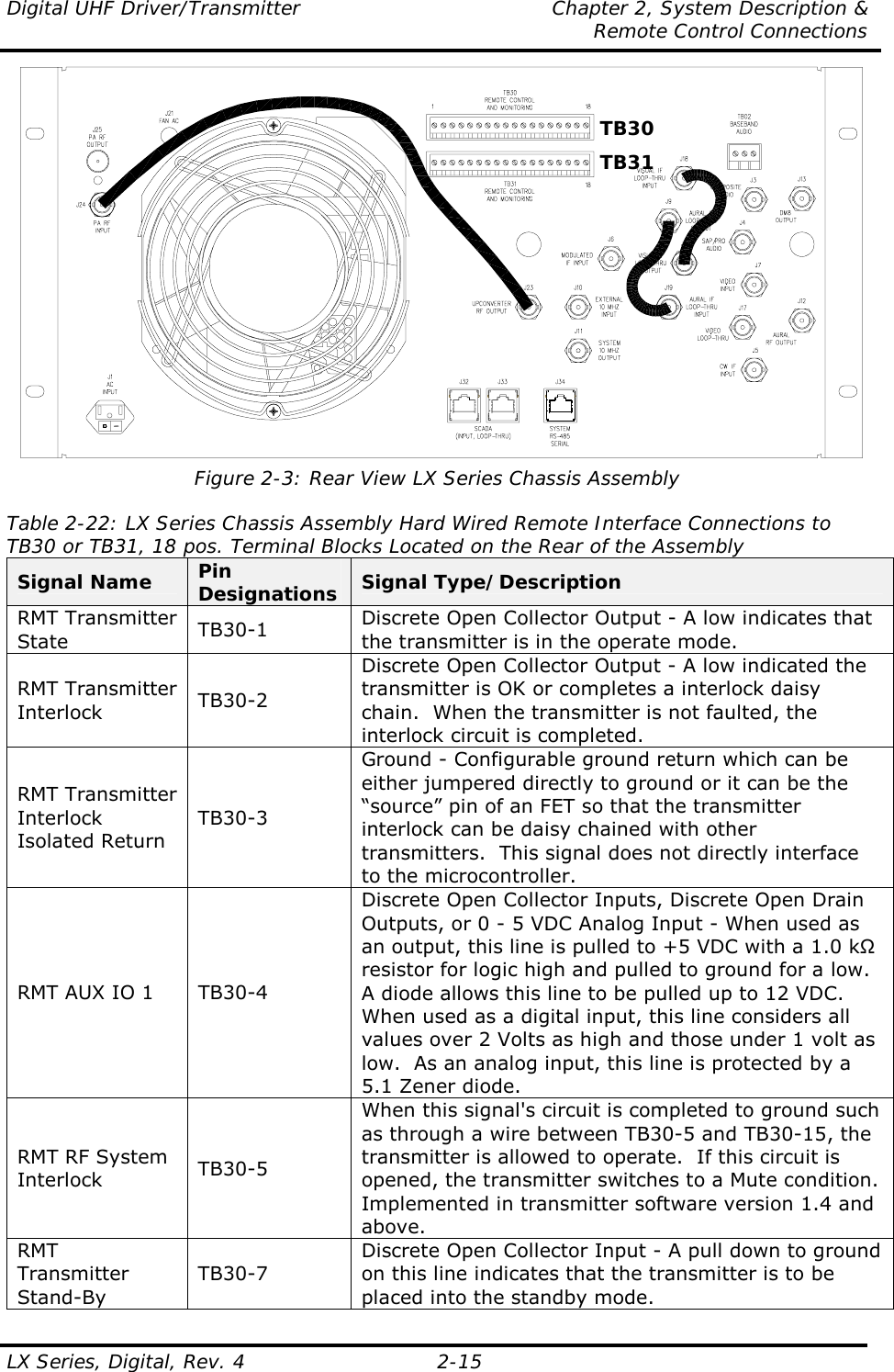
Contents

Users Manual Exciter with DM8 Modulator

 Instruction Manual                  Innovator, LX Series Digital UHF Driver/Transmitter             AXCERA, LLC  103 FREEDOM DRIVE, P.O. Box 525  LAWRENCE, PA 15055-0525 USA (724) 873-8100 • FAX (724) 873-8105 www.axcera.com • info@axcera.com
Digital UHF Driver/Transmitter    Table of Contents  LX Series, Digital, Rev. 4    March 8, 2007 i TABLE OF CONTENTS   CHAPTER 1  INTRODUCTION      SECTION    PAGE  1.1 Manual Overview...................................................................................1-1  1.2 Assembly Designation Numbers ..............................................................1-1  1.3 Safety..................................................................................................1-2  1.4 Contact Information ......................................................................... 1-2  1.5 Material Return Procedure ......................................................................1-2  1.6 Limited One Year Warranty for Axcera Products........................................1-3   CHAPTER 2  SYSTEM DESCRIPTION & REMOTE CONTROL CONNECTIONS   2.0  System Overview .................................................................................2-1  2.1 (Optional) Exciter Switcher Tray..............................................................2-2  2.2 Exciter Amplifier Chassis Assembly..........................................................2-3     2.2.1 DM8 Modulator Assembly..............................................................2-3     2.2.2 IF Processor Module .....................................................................2-4     2.2.3 VHF/UHF Upconverter Module........................................................2-6     2.2.4 Control & Monitoring/Power Supply Module.....................................2-7     2.2.5 Power Amplifier Module (In 5-50W Transmitters).............................2-8     2.2.6 Or Driver Amplifier Module (In High Power Transmitters)................2-10  2.3 RF Output Assemblies..........................................................................2-12  2.4 Control and Status...............................................................................2-12     2.4.1 Front Panel LCD Display Screen ...................................................2-12  2.5 System Operation................................................................................2-12     2.5.1 Principles of Operation................................................................2-12  2.6 Maintenance .......................................................................................2-14  2.7 Customer Remote Connections....................................................... 2-14       CHAPTER 3  SITE CONSIDERATIONS, INSTALLATION AND SETUP PROCEDURES     3.1 Site Considerations................................................................................3-1  3.2 Unpacking the Chassis w/Modules...........................................................3-5  3.3 Installing the Chassis w/Modules.............................................................3-5  3.4 AC Input...............................................................................................3-7  3.5 Setup and Operation..............................................................................3-8     3.5.1 Input Connections........................................................................3-8     3.5.2 Initial Turn On .............................................................................3-9     3.5.2.1 DM8 Digital Modulator Module LEDs on Front Panel.................3-9     3.5.2.2 IF Processor Module LEDs on Front Panel...............................3-9     3.5.2.3 VHF/UHF Upconverter Module LEDs on Front Panel .................3-9     3.5.2.4 Controller Module LEDs on Front Panel ................................3-10     3.5.2.5 Power Amplifier or Driver Module LEDs on Front Panel..........3-10     3.5.3 Front Panel Screens for the Exciter/Amplifier Chassis Assembly.......3-10     3.5.4 Operational Procedure ................................................................3-19   CHAPTER 4  CIRCUIT DESCRIPTIONS   4.0 (Optional) Exciter Switcher Tray..............................................................4-1     4.0.1 Exciter Switcher Control Board.......................................................4-1  4.1 DM8 Digital Modulator Module.................................................................4-1     4.1.1 Digital Modulator, DT1D Board.......................................................4-1     4.1.1.1 SMPTE-310 Input................................................................4-1
Digital UHF Driver/Transmitter    Table of Contents  LX Series, Digital, Rev. 4    March 8, 2007 iiTABLE OF CONTENTS - (Continued)              SECTION PAGE     4.1.1.2 Channel Coder....................................................................4-1     4.1.1.3 Analog Output Section.........................................................4-2     4.1.1.4 Pilot Frequency Generation...................................................4-2     4.1.1.5 Voltage Requirements .........................................................4-2     4.1.2 VSB Front Panel Board..................................................................4-3  4.2 IF Processor Module...............................................................................4-3     4.2.1 IF Processor Board .......................................................................4-3     4.2.1.1 DM8 Modulator Selected ......................................................4-3     4.2.1.2 External Modulated IF Selected.............................................4-3     4.2.1.3 Main IF Signal Path (Part 1 of 3)...........................................4-3     4.2.1.4 Input Level Detector Circuit..................................................4-4     4.2.1.5 Pin Diode Attenuator Circuit .................................................4-5     4.2.1.6 Main IF Signal Path (Part 2 of 3)...........................................4-5     4.2.1.7 Amplitude and Phase Pre Correction Circuits ..........................4-6     4.2.1.8 Main IF Signal Path (Part 3 of 3)...........................................4-7     4.2.1.9 ALC Circuit .........................................................................4-7     4.2.1.10 Fault Command.................................................................4-8     4.2.1.11 ±12 VDC Needed to Operate the Board ...............................4-8  4.3 VHF/UHF Upconverter Module.................................................................4-8     4.3.1 Downconverter Board ...................................................................4-9     4.3.2 L-Band PLL Board.........................................................................4-9     4.3.3 First Conversion Board..................................................................4-9     4.3.4 Upconverter Control Board ..........................................................4-10  4.4 Control Monitoring/Power Supply Module ...............................................4-10     4.4.1 Power Protection Board...............................................................4-11     4.4.2 Control Board ............................................................................4-12     4.4.2.1 Schematic Page 1..............................................................4-12     4.4.2.2 Schematic Page 2..............................................................4-12     4.4.2.3 Schematic Page 3..............................................................4-13     4.4.2.4 Schematic Page 4..............................................................4-13     4.4.2.5 Schematic Page 5..............................................................4-13     4.4.3 Switch Board .............................................................................4-14     4.4.4 Switching Power Supply Assembly................................................4-14  4.5 Power Amplifier Module Assembly (In 5-50W Transmitters) .....................4-14     4.5.1 1-Watt Amplifier Module Assembly...............................................4-14     4.5.2 1-Watt UHF Amplifier Board ........................................................4-15     4.5.3 40 Watt UHF Amplifier Assembly..................................................4-15     4.5.4 UHF Module Assembly, RF Module Pallet .......................................4-16     4.5.5 Coupler Board Assembly .............................................................4-16     4.5.6 Amplifier Control Board...............................................................4-16     4.5.6.1 Schematic Page 1..............................................................4-17     4.5.6.2 Schematic Page 2..............................................................4-17     4.5.6.3 Schematic Page 3..............................................................4-18  4.6 Or Driver Amplifier Module Assembly (In high power Transmitters)...........4-19     4.6.1 1-Watt Amplifier Module Assembly...............................................4-19     4.6.2 1-Watt UHF Amplifier Board ........................................................4-19     4.6.3 40 Watt UHF Amplifier Assembly..................................................4-20     4.6.3.1 250 Watt UHF Amplifier Assembly.......................................4-20     4.6.4 Coupler Board Assembly .............................................................4-21     4.6.5 Amplifier Control Board...............................................................4-21     4.6.5.1 Schematic Page 1..............................................................4-21
Digital UHF Driver/Transmitter    Table of Contents  LX Series, Digital, Rev. 4    March 8, 2007 iiiTABLE OF CONTENTS - (Continued)              SECTION PAGE     4.6.5.2 Schematic Page 2..............................................................4-22     4.6.5.3 Schematic Page 3..............................................................4-23  4.7 Dual Peak Detector Board.....................................................................4-23   CHAPTER 5  DETAILED ALIGNMENT PROCEDURES   5.1 System Preparation ...............................................................................5-1     5.1.1 Module Replacement.....................................................................5-1     5.1.2 Initial Test Set Up ........................................................................5-1  5.2 LX Series Exciter/Amplifier Chassis Assembly ...........................................5-1     5.2.1 IF Processor Module Assembly.......................................................5-2  5.3 Setting up the drive level of the transmitter up to 50 Watt.........................5-2     5.3.1 Setting up the Manual AGC............................................................5-2     5.3.2 Setting up the Auto AGC ...............................................................5-2  5.4 Changing the transmitter channel procedure ............................................5-3  5.5 Calibration of Output & Reflected Power for transmitters up to 50W............5-4     5.5.1 Calibration of Output Power for transmitters up to 50W....................5-5     5.5.2 Calibration of Reflected Power for transmitters up to 50W ................5-5  5.6 Setting ALC Gain, AGC1, AGC2 and AGC Cutback is Xmitrs above 50W .......5-5  5.7 Calibration of Output & Reflected Power for transmitters above 50W...........5-6     5.7.1 Calibration of Forward Power for transmitters above 50W.................5-6     5.7.2 Calibration of Reflected Power for transmitters above 50W ...............5-6  5.8 Linearity Correction Adjustment..............................................................5-7  5.9 Frequency Response Delay Equalization Adjustment..................................5-8  APPENDICES   APPENDIX A  INNOVATOR LX SERIES SPECIFICATIONS   APPENDIX B  DRAWINGS AND PARTS LISTS   APPENDIX C  TRANSMITTER LOG SHEET
Digital UHF Driver/Transmitter    Table of Contents  LX Series, Digital, Rev. 4 ivLIST OF FIGURES          FIGURE  PAGE  1-1   Brady Marker Identification Drawing.................................................1-1   2-1   Digital LX Series Front View Trays and Assemblies.............................2-1  2-2   Example of switching and displayed count with two faulted exciters.....2-2  2-3   Rear View LX Series Chassis Assembly............................................2-15   3-1   1 kW Minimum Ventilation Configuration...........................................3-4  3-2   Tray Slide Cabinet Mounting Diagram...............................................3-6  3-3   Front and Rear View Reconnection Drawing.......................................3-6  3-4   Cabinet Front and Rear View Reconnection Drawing...........................3-7  3-5   AC Input Box Assembly...................................................................3-7  3-6   Rear View of Exciter Driver..............................................................3-8   4-1   40 Watt UHF Amplifier Module .......................................................4-15  4-2   250 Watt UHF Amplifier Module .....................................................4-16  4-3   40 Watt UHF Amplifier Module .......................................................4-19  4-4   250 Watt UHF Amplifier Module .....................................................4-20   5-1   Typical Digital Spectrum .................................................................5-8
Digital UHF Driver/Transmitter    Table of Contents  LX Series, Digital, Rev. 4 v LIST OF TABLES         TABLE  PAGE  2-1   Digital LX Series Assemblies and Tray...............................................2-1  2-2   Digital Modulator Status Indicators...................................................2-4  2-3   Digital Modulator Sample ................................................................2-4  2-4   Digital Modulator Alignment Port......................................................2-4  2-5   IF Processor Front Panel Switch .......................................................2-5  2-6   IF Processor Front Panel Status Indicators ........................................2-5  2-7   IF Processor Front Panel Control Adjustments....................................2-5  2-8   IF Processor Front Panel Sample......................................................2-6  2-9   VHF/UHF Upconverter Front Panel Switch..........................................2-6  2-10 VHF/UHF Upconverter Front Panel Status Indicators...........................2-7  2-11 VHF/UHF Upconverter Front Panel Control Adjustments......................2-7  2-12 VHF/UHF Upconverter Front Panel Samples.......................................2-7  2-13 Controller/Power Supply Front Panel Display .....................................2-8  2-14 Controller/Power Supply Front Panel Status Indicators .......................2-8  2-15 Controller/Power Supply Front Panel Control Adjustments...................2-8  2-16 Power Amplifier Front Panel Status Indicators....................................2-9  2-17 Power Amplifier Front Panel Control Adjustments.............................2-10  2-18 Power Amplifier Front Panel Sample...............................................2-10  2-19 Driver Amplifier Front Panel Status Indicators..................................2-11  2-20 Driver Amplifier Front Panel Control Adjustments.............................2-11  2-21 Driver Amplifier Front Panel Sample...............................................2-11  2-22 LX Series Exciter Driver Customer Remote Connections.......... 2-15  2-23 (Optional) Exciter Switcher Customer Remote Connections.... 2-17   3-1   LX Series Digital Transmitters AC Input and Current Requirements......3-1  3-2   Rear Chassis Connections for LX Series Digital Exciter/Driver..............3-8 (Optional) Exciter Switcher Tray Menu Screens ...............................................3-10  3-3   Exciter Switcher Menu 01 Splash Screen #1....................................3-11  3-4   Menu 02 Splash Screen #2............................................................3-11  3-5   Menu 03 Exciter Switcher Control Screen, Automatic Operation.........3-11  3-6   Menu 04 Exciter Switcher Control Screen, Manual Operation.............3-11  3-7   Menu 05 Exciter Switcher Control Screen, Amps On Line ..................3-11  3-8   Menu 06 Exciter Switcher Control Screen, Cancel Auto Back up.........3-12  3-9   Menu 07 Exciter Switcher Control Screen, B Back up to A.................3-12  3-10 Menu 08 Exciter Switcher Control Screen, back up Changeover.........3-12  3-11 Menu 09 Exciter Switcher Control Screen, Ext Amp Status................3-12  3-12 Menu 10 Exciter Switcher Control Screen, Ext Amp Status................3-12 Digital Exciter/Driver System Controller Screens  3-13 Menu 01 Splash Screen #1............................................................3-13  3-14 Menu 02 Splash Screen #2............................................................3-13  3-15 Menu 10 Main Screen ...................................................................3-13  3-16 Menu 11 Error List Access Screen...................................................3-14  3-17 Menu 12 Transmitter Device Data Access Screen.............................3-14  3-18 Menu 13 Transmitter Configuration Access Screen...........................3-14  3-19 Menu 20 Error List Display Screen..................................................3-14  3-20 Menu 30 Transmitter Device Details Screen..................................3-15  3-21 Menu 30-1 System Details Screens..............................................3-15  3-22 Transmitter Device Parameters Detail Screens..............................3-15  3-23 Menu 40 Authorized Personnel Screen .........................................3-17  3-24 Menu 40-1 Transmitter Set Up: Power Control Screen ...................3-17  3-25 Menu 40-2 Transmitter Set Up: Model Select Screen .....................3-18
Digital UHF Driver/Transmitter    Table of Contents  LX Series, Digital, Rev. 4 viLIST OF TABLES – (continued)          TABLE ................................................................................................PAGE  3-26 Menu 40-3 Transmitter Set Up: Upconverter Channel Select Screen 3-18  3-27 Menu 40-4 Transmitter Set Up: Serial Address Screen...................3-18  3-28 Menu 40-6 Transmitter Set Up: System Forward Power Cal. Screen.3-18  3-29 Menu 40-6 Transmitter Set Up: System Reflected Power Cal. Screen.3-19  3-30 Menu 40-7 Transmitter Set Up: Fwrd Pwr Fault Threshold Screen......3-19  3-31 Menu 40-8 Transmitter Set Up: Refl Power Fault Threshold Screen....3-19  3-32 Menu 40-10 Transmitter Set Up: Auto Standby Control Screen .........3-19  3-33 Menu 40-12 Transmitter Set Up: Inner Loop Gain Control Screen......3-20  3-34 Menu 40-13 Transmitter Set Up: Optional System Control Screen .....3-20  3-35 Menu 40-14 Transmitter Set Up: DM 8 Optional Mode Control...........3-20  3-36 Menu 40-15 Transmitter Set Up: DM 8 Source Select Control............3-20  3-37 Menu 40-16 Transmitter Set Up: DM 8 Nonlinear Correction Control..3-20  3-38 Menu 40-16 Transmitter Set Up: DM 8 Fixed Table Selection Control .3-21  3-39 Menu 40-16 Transmitter Set Up: DM 8 Fixed Phase Selection Control 3-21  3-40 Menu 40-16 Transmitter Set Up: DM 8 Find Table Selection Control...3-21  3-41 Menu 40-17 Transmitter Set Up: DM 8 Linear Correction Control.......3-21  3-42 Menu 40-18 Transmitter Set Up: AGC Mode Control.........................3-21  3-43 Menu 40-19 Transmitter Set Up: Remote Commands Control............3-22
Digital UHF Driver/Transmitter    Chapter 1, Introduction  LX Series, Digital, Rev. 4  1-1 Chapter 1 Introduction  1.1 Manual Overview  This manual explains the installation, setup, alignment, and maintenance procedures for the LX Series modular Digital UHF driver/transmitter. If your transmitter contains external power amplifier assemblies, then information and drawings on the external amplifier assemblies are contained in Volume 2.  This instruction manual is divided into five chapters and supporting appendices. Chapter 1, Introduction, contains information on the assembly numbering system used in the manual, safety, maintenance, return procedures, and warranties. Chapter 2, system description, maintenance and remote control connections, describes the transmitter and includes discussions on system control and status indicators, maintenance and remote control connections. Chapter 3, site considerations, installation and setup procedures, explains how to unpack, install, setup, and operate the transmitter. Chapter 4, circuit descriptions, contains circuit-level descriptions for boards and board-level components in the transmitter. Chapter 5, Detailed Alignment Procedures, provides information on adjusting the system assemblies for optimal operation. Appendix A contains system specifications.  Appendix B contains drawings and parts lists.  Appendix C contains a transmitter log sheet 1.2 Assembly Designators  Axcera has assigned assembly numbers, Ax designations such as A1, where x=1,2,3…etc, to all assemblies, modules, and boards in the system.  These designations are referenced in the text of this manual and shown on the block diagrams and interconnect drawings provided in the appendices.  The Block Diagrams, Interconnects, Schematics, Assembly Drawings and Parts Lists are arranged in increasing numerical order in the appendices. Section titles in the text for assembly or module descriptions or alignment procedures contain the associated part number(s) and the relevant appendix that contains the drawings for that item.   The cables that connect between the boards within a tray or assembly and that connect between the trays, racks and cabinets are labeled using Brady markers.  Figure 1-1 is an example of a Brady marked cable.  There may be as few as two or as many as four Markers on any one cable.  These Brady markers are read starting furthest from the connector.  If there are four Brady Markers, this marker is the transmitter number such as transmitter 1 or transmitter 2.  The next or the furthest Brady Marker is the rack or cabinet number on an interconnect cable or the board number within a tray.  The next number on an interconnect cable is the Tray location or number.  The Brady marker closest to the connector is the jack or connector number on an interconnect cable or the jack or connector number on the board within a tray.  Figure 1-1 Brady Marker Identification Drawing
Digital UHF Driver/Transmitter    Chapter 1, Introduction  LX Series, Digital, Rev. 4  1-2 1.3 Safety  The UHF transmitter systems manufactured by Axcera are designed to be easy to use and repair while providing protection from electrical and mechanical hazards.  Please review the following warnings and familiarize yourself with the operation and servicing procedures before working on the transmitter system.  Read All safety Instructions – All of the safety instructions should be read and understood before operating this equipment.  Retain Manuals – The manuals for the transmitter should be retained at the transmitter site for future reference.  Axcera provides two sets of manuals for this purpose; one set can be left at the office while one set can be kept at the site.  Heed all Notes, Warnings, and Cautions – All of the notes, warnings, and cautions listed in this safety section and throughout the manual must be followed.  Follow Operating Instructions – All of the operating and use instructions for the transmitter should be followed.  Cleaning – Unplug or otherwise disconnect all power from the equipment before cleaning.  Do not use liquid or aerosol cleaners.  Use a damp cloth for cleaning.  Ventilation – Openings in the cabinet and module front panels are provided for ventilation.  To ensure the reliable operation of the driver/transmitter, and to protect the unit from overheating, these openings must not be blocked.  Servicing – Do not attempt to service this product yourself until becoming familiar with the equipment.  If in doubt, refer all servicing questions to qualified Axcera service personnel. Replacement Parts – When replacement parts are used, be sure that the parts have the same functional and performance characteristics as the original part.  Unauthorized substitutions may result in fire, electric shock, or other hazards.  Please contact the Axcera Technical Service Department if you have any questions regarding service or replacement parts.  1.4 Contact Information  The Axcera Field Service Department can be contacted by phone at (724) 873-8100 or by fax at (724) 873-8105.    Before calling Axcera, please be prepared to supply the Axcera technician with answers to the following questions.  This will save time and help ensure the most direct resolution to the problem.  1.  What are the Customers’ Name and call letters? 2.  What are the model number and type of transmitter? 3.  Is the transmitter digital or analog? 4.  How long has the transmitter been on the air? (Approximately when was the transmitter installed.) 5.  What are the symptoms being exhibited by the transmitter? Include the current control/power supply LCD readings and the status of LEDs on the front panels of the modules.  If possible, include the control/power supply LCD readings before the problem occurred.  1.5 Return Material Procedure  To insure the efficient handling of equipment or components that have been returned for repair, Axcera requests that each returned item be accompanied by a Return Material Authorization Number (RMA#).
Digital UHF Driver/Transmitter    Chapter 1, Introduction  LX Series, Digital, Rev. 4  1-3 The RMA# can be obtained from any Axcera Field Service Engineer by contacting the Axcera Field Service Department at (724) 873-8100 or by fax at (724) 873-8105.  This procedure applies to all items sent to the Field Service Department regardless of whether the item was originally manufactured by Axcera.  When equipment is sent to the field on loan, an RMA# is included with the unit. The RMA# is intended to be used when the unit is returned to Axcera.  In addition, all shipping material should be retained for the return of the unit to Axcera.   Replacement assemblies are also sent with an RMA# to allow for the proper routing of the exchanged hardware. Failure to close out this type of RMA# will normally result in the customer being invoiced for the value of the loaner item or the exchanged assembly.  When shipping an item to Axcera, please include the RMA# on the packing list and on the shipping container.  The packing slip should also include contact information and a brief description of why the unit is being returned.  Please forward all RMA items to:  AXCERA, LLC  103 Freedom Drive P.O. Box 525 Lawrence, PA 15055-0525  USA  For more information concerning this procedure, call the Axcera Field Service Department @ (724) 873-8100. Axcera can also be contacted through e-mail at info@axcera.com and on the Web at www.axcera.com.  1.6 Limited One Year Warranty for Axcera Products  Axcera warrants each new product that it has manufactured and sold against defects in material and workmanship under normal use and service for a period of one (1) year from the date of shipment from Axcera's plant, when operated in accordance with Axcera's operating instructions.  This warranty shall not apply to tubes, fuses, batteries, bulbs or LEDs.  Warranties are valid only when and if (a) Axcera receives prompt written notice of breach within the period of warranty, (b) the defective product is properly packed and returned by the buyer (transportation and insurance prepaid), and (c) Axcera determines, in its sole judgment, that the product is defective and not subject to any misuse, neglect, improper installation, negligence, accident, or (unless authorized in writing by Axcera) repair or alteration.  Axcera's exclusive liability for any personal and/or property damage (including direct, consequential, or incidental) caused by the breach of any or all warranties, shall be limited to the following: (a) repairing or replacing (in Axcera's sole discretion) any defective parts free of charge (F.O.B. Axcera’s plant) and/or (b) crediting (in Axcera's sole discretion) all or a portion of the purchase price to the buyer.  Equipment furnished by Axcera, but not bearing its trade name, shall bear no warranties other than the special hours-of-use or other warranties extended by or enforceable against the manufacturer at the time of delivery to the buyer.  NO WARRANTIES, WHETHER STATUTORY, EXPRESSED, OR IMPLIED, AND NO WARRANTIES OF MERCHANTABILITY, FITNESS FOR ANY PARTICULAR PURPOSE, OR FREEDOM FROM INFRINGEMENT, OR THE LIKE, OTHER THAN AS SPECIFIED IN PATENT LIABILITY ARTICLES, AND IN THIS ARTICLE, SHALL APPLY TO THE EQUIPMENT FURNISHED HEREUNDER.
Digital UHF Driver/Transmitter    Chapter 1, Introduction  LX Series, Digital, Rev. 4  1-4  !!!! WARNING!!!   """" HIGH VOLTAGE ####  DO NOT ATTEMPT TO REPAIR OR TROUBLESHOOT THIS EQUIPMENT UNLESS YOU ARE FAMILIAR WITH ITS OPERATION AND EXPERIENCED IN SERVICING HIGH VOLTAGE EQUIPMENT.  LETHAL VOLTAGES ARE PRESENT WHEN POWER IS APPLIED TO THIS SYSTEM.  IF POSSIBLE, TURN OFF POWER BEFORE MAKING ADJUSTMENTS TO THE SYSTEM.    $$$$ RADIO FREQUENCY RADIATION HAZARD $$$$  MICROWAVE, RF AMPLIFIERS AND TUBES GENERATE HAZARDOUS RF RADIATION THAT CAN CAUSE SEVERE INJURY INCLUDING CATARACTS, WHICH CAN RESULT IN BLINDNESS.  SOME CARDIAC PACEMAKERS MAY BE AFFECTED BY THE RF ENERGY EMITTED BY RF AND MICROWAVE AMPLIFIERS.  NEVER OPERATE THE TRANSMITTER SYSTEM WITHOUT A PROPERLY MATCHED RF ENERGY ABSORBING LOAD ATTACHED.  KEEP PERSONNEL AWAY FROM OPEN WAVEGUIDES AND ANTENNAS.  NEVER LOOK INTO AN OPEN WAVEGUIDE OR ANTENNA.  MONITOR ALL PARTS OF THE RF SYSTEM FOR RADIATION LEAKAGE AT REGULAR INTERVALS.
Digital UHF Driver/Transmitter    Chapter 1, Introduction  LX Series, Digital, Rev. 4  1-5  EMERGENCY FIRST AID INSTRUCTIONS  Personnel engaged in the installation, operation, or maintenance of this equipment are urged to become familiar with the following rules both in theory and practice.  It is the duty of all operating personnel to be prepared to give adequate Emergency First Aid and thereby prevent avoidable loss of life.      RESCUE BREATHING  1. Find out if the person is breathing.  You must find out if the person has stopped breathing. If you think he is not breathing, place him flat on his back. Put your ear close to his mouth and look at his chest. If he is breathing you can feel the air on your cheek. You can see his chest move up and down. If you do not feel the air or see the chest move, he is not breathing.      2. If he is not breathing, open the airway by tilting his head backwards.   Lift up his neck with one hand and push down on his forehead with the other. This opens the airway. Sometimes doing this will let the person breathe again by himself.  3. If he is still not breathing, begin rescue breathing.  -Keep his head tilted backward. Pinch nose shut. -Put your mouth tightly over his mouth. -Blow into his mouth once every five seconds -DO NOT STOP rescue breathing until help arrives.  LOOSEN CLOTHING - KEEP WARM  Do this when the victim is breathing by himself or help is available. Keep him as quiet as possible and from becoming chilled. Otherwise treat him for shock.   BURNS  SKIN REDDENED: Apply ice cold water to burned area to prevent burn from going deeper into skin tissue. Cover area with a clean sheet or cloth to keep away air. Consult a physician.  SKIN BLISTERED OR FLESH CHARRED: Apply ice cold water to burned area to prevent burn from going deeper into skin tissue. Cover area with clean sheet or cloth to keep away air. Treat victim for shock and take to hospital.  EXTENSIVE BURN - SKIN BROKEN: Cover area with clean sheet or cloth to keep away air. Treat victim for shock and take to hospital.
Digital UHF Driver/Transmitter    Chapter 1, Introduction  LX Series, Digital, Rev. 4  1-6  dBm, dBw, dBmV, dBµµµµV, & VOLTAGE EXPRESSED IN WATTS   50 Ohm System  WATTS PREFIX dBm dBw dBmV dBµV VOLTAGE1,000,000,000,000 1 TERAWATT  +150 +120          100,000,000,000  100 GIGAWATTS  +140 +110            10,000,000,000  10 GIGAWATTS  +130 +100              1,000,000,000  1 GIGAWATT  +120 + 99                 100,000,000  100 MEGAWATTS  +110 + 80                   10,000,000  10 MEGAWATTS  +100 + 70                     1,000,000  1 MEGAWATT  + 90  + 60                        100,000  100 KILOWATTS  + 80  + 50                         10,000  10 KILOWATTS  + 70  + 40                           1,000  1 KILOWATT  + 60  + 30                              100  1 HECTROWATT  + 50  + 20                                50   + 47  + 17                                20   + 43  + 13                                10  1 DECAWATT  + 40  + 10                                  1  1 WATT  + 30  0  + 77  +137  7.07V                         0.1  1 DECIWATT  + 20  - 10  + 67  +127  2.24V                       0.01  1 CENTIWATT  + 10  - 20  + 57  +117  0.707V                     0.001  1 MILLIWATT  0  - 30  + 47  +107  224mV                   0.0001  100 MICROWATTS  - 10  - 40                        0.00001  10 MICROWATTS  - 20  - 50                      0.000001  1 MICROWATT  - 30  - 60                    0.0000001  100 NANOWATTS  - 40  - 70                  0.00000001  10 NANOWATTS  - 50  - 80                0.000000001  1 NANOWATT  - 60  - 90              0.0000000001  100 PICOWATTS  - 70  -100            0.00000000001  10 PICOWATTS  - 80  -110          0.000000000001  1 PICOWATT  - 90  -120         TEMPERATURE CONVERSION   °°°°F = 32 + [(9/5) °°°°C]  °°°°C = [(5/9) (°°°°F - 32)]
Digital UHF Driver/Transmitter    Chapter 1, Introduction  LX Series, Digital, Rev. 4  1-7 USEFUL CONVERSION FACTORS  TO CONVERT FROM  TO   MULTIPLY BY       mile (US statute)          kilometer (km)           1.609347      inch (in)            millimeter (mm)          25.4        inch (in)            centimeter (cm)          2.54       inch (in)            meter (m)              0.0254      foot (ft)            meter (m)              0.3048      yard (yd)            meter (m)              0.9144      mile per hour (mph)        kilometer per hour(km/hr)         1.60934      mile per hour (mph)        meter per second (m/s)          0.44704      pound (lb)            kilogram (kg)                 0.4535924      gallon (gal)           liter                   3.7854118         U.S. liquid          (One U.S. gallon equals 0.8327 Canadian gallon)      fluid ounce (fl oz)         milliliters (ml)                   29.57353      British Thermal Unit       watt (W)                   0.2930711                               per hour (Btu/hr)      horsepower (hp)         watt (W)                              746  NOMENCLATURE OF FREQUENCY BANDS   FREQUENCY RANGE    DESIGNATION      3 to 30 kHz        VLF  -  Very Low Frequency   30 to 300 kHz    LF -  Low Frequency     300 to 3000 kHz      MF  -  Medium Frequency   3 to 30 MHz    HF -  High Frequency     30 to 300 MHz      VHF  -  Very High Frequency     300 to 3000 MHz      UHF  -  Ultrahigh Frequency   3 to 30 GHz    SHF -  Superhigh Frequency      30 to 300 GHz      EHF  -  Extremely High Frequency  LETTER DESIGNATIONS FOR UPPER FREQUENCY BANDS  LETTER     FREQ. BAND            L            1000 - 2000 MHz           S            2000 - 4000 MHz           C            4000 - 8000 MHz           X            8000 - 12000 MHz           Ku           12 - 18 GHz           K            18 - 27 GHz           Ka           27 - 40 GHz           V            40 - 75 GHz           W           75 - 110 GHz
Digital UHF Driver/Transmitter    Chapter 1, Introduction  LX Series, Digital, Rev. 4  1-8     RETURN LOSS VS. VSWR         1.001            1.01          1.1               2.0               VSWR   0   -10   -20 -30   -40   -50   -60      -70 RETURN  LOSS  dB
Digital UHF Driver/Transmitter     Chapter 1, Introduction  LX Series, Digital, Rev. 4  1-9 ABBREVIATIONS/ACRONYMS  AC  Alternating Current  AFC  Automatic Frequency Control  ALC  Automatic Level Control  AM  Amplitude modulation  AGC  Automatic Gain Control  AWG  American wire gauge  BER  Bit Error Rate  BW  Bandwidth  DC  Direct Current  D/A  Digital to analog  DSP  Digital Signal Processing  DTV  Digital Television  dB  Decibel  dBm  Decibel referenced to 1 milliwatt  dBmV  Decibel referenced to 1 millivolt  dBw  Decibel referenced to 1 watt  FEC  Forward Error Correction  FM  Frequency modulation  FPGA  Field Programmable Gate Array  Hz  Hertz  ICPM  Incidental Carrier Phase Modulation  I/P  Input  IF  Intermediate Frequency LED  Light emitting diode  LSB  Lower Sideband  MPEG  Motion Pictures Expert Group  O/P  Output  PLL  Phase Locked Loop  PCB  Printed circuit board  QAM  Quadrature Amplitude Modulation  SMPTE  Society of Motion Picture and     Television Engineers  VSB Vestigial Side Band
Digital UHF Driver/Transmitter  Chapter 2, System Description &   Remote Control Connections LX Series, Digital, Rev. 4    2-1 Chapter 2 System Description & Remote Control Connections  2.0 System Overview  The LX Series are complete Digital UHF modular television transmitters that operate at an average output power of 5 Watts to 50 Watts.   When used as a driver, it operates at the needed drive level to produce the desired output power level of the PA Assembly or Assemblies.  The model number scheme for a Innovator LX Series transmitter is as follows (where #### = power in watts):   LU####ATD  - LX Series UHF Digital Xmtr  (Example): LU50ATD is a 50 Watt Digital UHF Xmtr  The LX Series digital transmitter is made up of the modules and assemblies as listed in Table 2-1 and shown in Figure 2-1.    Figure 2-1: Digital LX Series Front View Trays and Assemblies  Table 2-1: Digital LX Series Trays and Assemblies ASSEMBLY DESIGNATOR  TRAY/ASSEMBLY NAME  PART NUMBER  Chassis Assembly  1304052 (110 VAC) or 1304053 (220 VAC A1  DM8 Digital Modulator Module  1306342 A3 IF Processor Module 1301938 A4  Control & Monitoring/Power Supply Module 1301936 (110 VAC) or 1303229 (220 VAC) A5 VHF/UHF Upconverter Module 1303829 A6  Power Amplifier Module for 5-50 Watt Transmitter  1303770 OR A6 Driver Amplifier Module for High Power Transmitter 1303771 (1kW), 1303874 (2kW) OR 1303770 (3kW & above) A11  Backplane Board, V2, LX Series  1304047  A1 A3 A5 A4 A6
Digital UHF Driver/Transmitter  Chapter 2, System Description &   Remote Control Connections LX Series, Digital, Rev. 4    2-2 2.1 (Optional) Exciter Switcher Tray, 110 VAC (1305727) or 220 VAC (1305715); Appendix B  The (optional) Single Channel Auto Switcher is part of the dual exciter system.  The assembly is made up of (A1) a Single Channel Exciter Switcher Tray (1305715) with a separate (A2) coaxial transfer relay, mounted on a bracket that faces toward the rear of the cabinet, behind the Switcher Tray.  The tray is factory set for the proper voltage.  Exciter Switcher operations when it is in 'Automatic Operation' have changed in version 2.0 or newer.  Older versions of the switcher code would change exciters if the primary exciter reported any fault and the back-up exciter did not have any entries in its fault log.  Versions 2.0 and greater now rely on the reported output power of the selected exciter to determine if a changeover is required.  If the On Air Exciter should malfunction, due to the driver stage of the On Air Exciter reporting less that 50% power while that specific exciter is enabled and has been so enabled for more than 30 seconds, the Exciter Switcher will attempt to switch to the Back Up Exciter 3 times, each time checking its status.  If after 3 times the back up exciter is not operational the exciter switcher changeover function will be disabled for 5 minutes.  After 5 minutes it will start again to switch between exciters.  Figure 2-2. Example of switching and displayed count with two faulted exciters:                      Remote and front panel exciter changes are permitted during the 5 minute lockout of the automatic exciter changes.  If the exciter switcher is placed into Manual mode, all exciter change counters and the lockout counter are cleared.  There is a built in 30 second delay from when the Exciter is changed from Standby to Operate to allow for the determination that the selected Exciters Driver PA is generating 50% output power or more.  The numbers shown on the Upper right of the second LCD screen indicates that the Exciter has switched that many times.  An L indicates that the 5 Minute Lock Out has occurred.  The default main menu will typically show 'MANUAL OPERATION', or 'AUTOMATIC Exciter A: Becomes FaultedExciter B: FaultedExciter A: FaultedExciter B: FaultedExciter Change 1: Counter 1 set Exciter Change 2: Counter 2 set Exciter Change 3: Counter 3 set No Exciter Change for 5 minutes
Digital UHF Driver/Transmitter  Chapter 2, System Description &   Remote Control Connections LX Series, Digital, Rev. 4    2-3 OPERATION', or 'AUTOMATIC LOCK XXX' where xxx is the number of seconds before the exciter can again automatically switch between exciters.  During this time the switcher will not automatically switch.  An indication of 123L means that a 3 Fault has occurred and the 5 minute lock out is in effect.  Timers do not prevent manual switching of the exciters thru the remote or the front panel.  If the switcher attempts to change exciters and the backup exciter is not present or it does not change to operate after the relay positions are changed, the switcher returns to the primary exciter, enables the primary exciter and then locks out further exciter changes for 5 minutes.  Menu 2 is new.  It reports the status of the exciters.  They can either be not present is indicated by a 'NO COM (OFFLINE)' message, in the standby mode, or in the operate mode as indicated by the display of the driver output power.  For the first 30 seconds of operate mode, the switcher will indicate the number of seconds remaining in the 30 second countdown.  After 30 seconds of operation, the display will indicate the number of current faults on the exciter.  These faults are all inclusive and may indicate problems with the external amplifier, therefore it is possible to see a number of current faults but the driver power to be greater than 50% and the exciter to remain in use.  The coaxial relay has the RF outputs from both Exciters connected to its inputs and, depending on if the energizing voltage is applied or not, the selected Exciter RF Output is connected to the external amplifiers and the RF output from the other exciter is connected to a load.  The front panel has a 4 x 20 display providing a four-line readout of the operation and control of the exciter switcher.  The LCD screens are detailed in Chapter 3.   2.2 Exciter Amplifier Chassis Assembly, V2, {1304052 (110 VAC) or 1304053 (220 VAC); Appendix B}  The chassis assembly is factory set for operation using 110 VAC or 220 VAC.  All of the modules, except the power amplifier module and the power supply section of the Control & Monitoring/Power Supply Module, plug directly into a backplane board.  The backplane board provides module to module interconnection as well as interconnection to remote command and control connectors.  2.2.1 DM-8 Modulator Assembly, DT1D (1306342; Appendix B)   The DM8 modulator is an ATSC compliant 8 VSB modulator that slides into the left most slot in the Innovator LX Driver chassis assembly.  The DM8 modulator accepts a SMPTE-310 MPEG data stream input and outputs a 6 MHz wide IF output centered at 44 MHz with a pilot carrier at 46.69 MHz.  The DM8 modulator provides linear and nonlinear correction capability for the transmission path as well as internal test sources that are used during initial transmitter installation.  All of the functions of the DM8 modulator are controlled from the LX Controller LCD display and pushbuttons.
Digital UHF Driver/Transmitter  Chapter 2, System Description &   Remote Control Connections LX Series, Digital, Rev. 4    2-4 Table 2-2. Digital Modulator Status Indicators LED FUNCTION MPEG (Green)  Indicates the presence of a valid MPEG stream at the J1-2B input jack. PLL A (Green)  Indicates that the DM8 symbol clock is locked to the frequency of the 10 MHz reference. PLL B (Green)  Indicates that the pilot frequency is locked to the incoming 10 MHz reference. Table 2-3. Digital Modulator Sample SAMPLE DESCRIPTION IF Sample  Provides a sample of the IF output from the modulator at approximately a –20 dBm level.  Table 2-4. Digital Modulator Alignment Port PORT DESCRIPTION RS-232  Serial port used for the initial DM8 modulator alignment.  2.2.2 (A3) IF Processor Module Assembly (1301938; Appendix B)   The (A3) IF Processor Assembly contains the IF Processor Board (1301977). The IF Processor provides pre-correction to ensure broadcast quality output signal. The pre-correction consists of amplitude linearity correction, Incidental Carrier Phase Modulation (ICPM) correction and frequency response correction.  The IF Processor module is configured either for an analog or digital system.  Pin 13C of the IF Processor module is grounded in analog systems and left not connected in digital systems.  An IF Processor Interlock signal is used to report the presence of the IF Processor module to the Control Monitoring board.  If the IF Processor interlock signal is not present, the LX Series Transmitter Exciter Driver RF output is Muted (turned off).  The Control & Monitoring/Power Supply module uses the IF Processor module for System output power control.  Through the front panel display or a remote interface, an operator can set the transmitter's RF output power.  The range of RF power adjustment is between 0% (full off) and 105% (full power plus).  A front panel IF Processor module potentiometer sets the upper limit of RF power at 120%.  The system's Control Monitoring board compares the RF Power Monitoring module RF power level with the desired level and uses the IF Power Control PWM line to correct for errors.   In digital systems, a digital level control (DLC) voltage is generated on the IF Processor module and sent to the digital modulator.  RF power control is implemented by changing the DLC voltage provided to the digital modulator.  The 'RF High' potentiometer sets the upper adjusted range of RF control circuit output to 120%.   The IF Processor module provides a reference ALC voltage to the system's Upconverter.  When the ALC voltage
Digital UHF Driver/Transmitter  Chapter 2, System Description &   Remote Control Connections LX Series, Digital, Rev. 4    2-5 decreases, the Upconverter automatically lowers the system output power through the AGC circuits.  The IF Processor module has a front panel switch to select Auto or Manual ALC.  When Manual ALC is selected, the reference ALC voltage is set by a front panel potentiometer.  In this condition, the RF power level control circuit is removed from use.  When the ALC select switch is changed to Auto, the RF power level control circuit will start at low power and increase the RF output until the desired output power is attained.  The IF Processor module Modulation Present signal is monitored.  If the modulation level is too low or non-existent, a Modulation Present fault is reported to the Control Monitoring board.  When the controller detects this fault, it can be set to Automatically Mute the transmitter or in Manual mode the transmitter will continue to operate at 25% output.   The IF Processor module Input Signal level is monitored.  If the signal level is too low or non-existent, an Input fault is reported on the Control Monitoring board.  When the IF Processor board detects an Input Signal fault it automatically Mutes the transmitter.  The system controller does not Mute on an IF Processor Input fault. Table 2-5. IF Processor Front Panel Switch SWITCH FUNCTION MAN/AUTO ALC When Manual ALC is selected, the reference ALC voltage is set by the ALC Gain front panel potentiometer.   When Auto ALC is selected, the IF level control circuit will automatically increase the IF output until the desired output power is attained.   Table 2-6. IF Processor Front Panel Status Indicators LED FUNCTION INPUT FAULT (Red)  When lit it indicates that there is a loss of the IF Input signal to the IF Processor.  Transmitter can be set to Mute on an IF Input Fault. ALC Fault (Red) When lit it indicates that the required gain to produce the desired output power level has exceeded the operational range of the ALC circuit.  The LED will also be lit when ALC is in Manual. MUTE (Red)  When lit it indicates that the IF input signal is cut back but the enable to the Power Supply is present and the +32 VDC remains on. Table 2-7. IF Processor Front Panel Control Adjustments POTENTIOMETERS DESCRIPTION FREQUENCY RESPONSE EQUALIZER These three variable resistors, R103, R106 & R274, adjust the depth of gain for the three stages of frequency response correction. ALC GAIN  Adjusts the gain of the transmitter when the transmitter is in the Auto ALC position. MAN GAIN  Adjusts the gain of the transmitter when the transmitter is in the Manual ALC position. LINEARITY CORRECTION These three variable resistors adjust the threshold cut in for the three stages of linearity pre-correction.  R211 and R216, the top two pots, are adjusted to correct for in phase amplitude distortions.  R 231, the bottom pot, is adjusted to correct for quadrature phase distortions.
Digital UHF Driver/Transmitter  Chapter 2, System Description &   Remote Control Connections LX Series, Digital, Rev. 4    2-6 Table 2-8. IF Processor Front Panel Sample SMA CONNECTOR  DESCRIPTION IF SAMPLE  Sample of the pre-corrected IF output of the IF Processor  2.2.3 (A5) VHF/UHF Upconverter Module Assembly (1303829; Appendix B)     The VHF/UHF Upconverter Module Assembly contains (A1) a Downconverter Board Assembly (1303834), (A3) a First Conversion Board, LX Series (1303838), (A2) a L-Band PLL Board, LX Series (1303846) and (A4) an Upconverter Control Board (1304760).  A 0 dBm 44 MHz IF input to the upconverter through the backplane board is applied to a mixer mounted on the first conversion board.  Also applied to the mixer is a nominal 1 GHz LO1.  The mixer converts it to a nominal frequency centered at 1044 MHz.  A filter selects the appropriate conversion product, which is then amplified to a level of approximately –4 dBm.  The frequency of the first conversion LO1 can be shifted by ± 10 kHz to generate channel offsets of 10kHz.  For +offsets the frequency is 999.99 MHz and for –offsets the frequency is 1000.01 MHz.  This signal is applied to a second mixer mounted on the downconverter board that converts it back to a broadcast channel (2-69) by an LO2 that operates in 100kHz steps between 1.1-1.9 GHz depending on the channel selected.  The LO2 frequency equals the Channel center frequency plus the LO1 frequency plus 44 MHz.  (As an example CH14+: Center Frequency is 473.01 MHz and LO1 is 999.99 MHz therefore LO2 is 473.01 + 999.99 + 44, which equals 1517.00 MHz.)  The output of the mixer is applied to a 900 MHz Low pass filter to remove unwanted conversion products.  The resulting signal is amplified and applied to a Pin diode attenuator before it is connected to the output of the upconverter.  This pin diode attenuator adjusts the gain of the module and is controlled by an Automatic Gain Control circuit, which maintains a constant power out of the upconverter, and also the transmitter, that connects to the power amplifier module.   Table 2-9. VHF/UHF Upconverter Front Panel Switch SWITCH FUNCTION MAN/AUTO AGC (Left Manual, Right AGC) When Manual AGC is selected, the reference AGC voltage is set by the AGC Manual Gain front panel potentiometer.   When Auto AGC is selected, the RF power level control circuit will automatically increase the RF output until the desired output power is attained.
Digital UHF Driver/Transmitter  Chapter 2, System Description &   Remote Control Connections LX Series, Digital, Rev. 4    2-7  Table 2-10. VHF/UHF Upconverter Front Panel Status Indicators LED FUNCTION PLL 1 Fault (Red)  When lit it indicates that the 1 GHz PLL is unlocked PLL 2 Fault (Red)  When lit it indicates that the 1.1 –1.9 GHz PLL is unlocked AGC Fault (Red)  When lit it indicates that the AGC is out of range. AGC Override (Red) When lit it indicates that the AGC is cutting back due to too much drive to the driver module. Man Gain (Amber)  When lit it indicates that the AGC is bypassed in Manual.  Table 2-11. VHF/UHF Upconverter Front Panel Control Adjustments POTENTIOMETERS DESCRIPTION MAN GAIN ADJ  Adjusts the gain of the upconverter and transmitter when in the Manual AGC position. AGC ADJ  Adjusts the gain of the upconverter and transmitter when in the Auto AGC position. AGC CUTBACK ADJ (AGC OVERRIDE) Adjusts the point at which the transmitter will cut back in power, due to too much drive, when the Transmitter is in Auto AGC.  Table 2-12. VHF/UHF Upconverter Front Panel Samples SMA CONNECTOR  DESCRIPTION LO1 SAMPLE  Sample of the 1 GHz nominal LO1 signal in the Upconverter as generated on the L-Band PLL Board. LO2 SAMPLE  Sample of the 1.1-1.9 GHz LO2 signal in the Upconverter as generated on the First Conversion Board. RF SAMPLE  Sample of the On Channel RF Output of the Upconverter  2.2.4 (A4) Control & Monitoring/ Power Supply Module Assembly {1301936 (110VAC) or 1303229 (220VAC); Appendix B}    8 A4 A  The (A4) Control & Monitoring/Power Supply Assembly is made up of a Control Board (1302021), a Power Protection Board (1302837) and a Switch Board (1527-1406).  The Assembly also contains a switching power supply that provides ±12 VDC to the rest of the modules in the chassis and +32 VDC to the Power Amplifier module.  The Assembly provides all transmitter control and monitoring functions.  The Front panel LCD allows monitoring of system parameters, including forward and reflected power, transistor currents, module temperatures and power supply voltages.
Digital UHF Driver/Transmitter  Chapter 2, System Description &   Remote Control Connections LX Series, Digital, Rev. 4    2-8 Table 2-13. Controller/Power Supply Display DISPLAY FUNCTION LCD A 4 x 20 display providing a four-line readout of the internal functions, external inputs, and status. See Chapter 3, Controller/Power Supply Display Screens, for a listing of displays.  Table 2-14. Controller/Power Supply Status Indicator LED FUNCTION OPERATE ( green ) When lit it indicates that the transmitter is in the Operate Mode.  If transmitter is Muted the Operate LED will stay lit, the transmitter will remain in Operate, until the input signal is returned. FAULT ( red or green ) Red indicates that a problem has occurred in the transmitter.  The transmitter will be Muted or placed in Standby until the problem is corrected. DC OK ( red or green ) Green indicates that the switchable fuse protected DC outputs that connect to the modules in the transmitter are OK.  Table 2-15. Controller/Power Supply Control Adjustments POTENTIOMETERS DESCRIPTION DISPLAY CONTRAST  Adjusts the contrast of the display for desired viewing of screen.  2.2.5 (A6) Power Amplifier Module Assembly, Exciter, 5W-50W Transmitter (1303770; Appendix B)    NOTE: The (A6) Driver Amplifier Module Assembly (1303771) replaces the Power Amplifier Module Assembly (1303770) in High Power Transmitters.  It is also used as a driver in 3kW or higher transmitters.  The (A6) Power Amplifier Module Assembly is made up of a Coupler Board Assembly (1301949), an Amplifier Control Board (1303682), a 1 Watt Module Assembly (1302891), a 40W UHF Module (1304490) and a RF Module Pallet, Philips (1300116).  The Power Amplifier Module contains Broadband LDMOS amplifiers that cover the entire UHF band with no tuning required. They amplify the RF to the 10W to 50W output power level of the transmitter.  The Power Amplifier of the Transmitter/Exciter Driver is used to amplify the RF output of the Upconverter module.  A cable, located on the rear chassis, connects the RF output from the Upconverter at J23 to J24 the RF input to the PA Assembly.  This module contains RF monitoring circuitry for both an analog and a digital system.  Control and monitoring lines to the Power Amplifier module are routed through the floating blind-mate connector of the Control & Monitoring/Power Supply module.  The 50 Watt Transmitter/Exciter Driver Power Amplifier module and any External Amplifier modules contain the same control and monitoring board.  This board monitors RF output power, RF reflected power, the current draw of
Digital UHF Driver/Transmitter  Chapter 2, System Description &   Remote Control Connections LX Series, Digital, Rev. 4    2-9 amplifier sections, the supply voltage, and the temperature of the PA heat sink.  The RF power detector circuit outputs vary with operating frequency.  These circuits must be calibrated at their intended operating frequency.  Front panel adjustment potentiometers are used to calibrate the following:  Power Amplifier Calibration Adjustments  R201  Reflected Power Cal R202  Forward Power Cal R203  (NOT USED) Aural Power Cal R205  (NOT USED) Aural Null  the Forward power of an Exciter Driver Power Amplifier and the Forward power of any external amplifier, is reported by the system Control Monitoring module.   If the Control Monitoring module is monitoring a 5-50 Watt Transmitter, system power is measured in the Power Amplifier module.  The wired connections are transferred through the power supply connector to the backplane board on a five position header.  All four positions of control board switch SW1 must be set on to route these lines as the system's RF power signals.  In systems of output power greater than 50 Watts, system power is monitored by an external module that is connected to TB31 and control board SW1 switches must be set off.   The Forward Power of the Transmitter/Exciter Driver Power Amplifier module is routed to the Upconverter module as AGC #1.  A system over-drive condition is detected when this value rises above 0.9 VDC.  When an over-drive condition is detected, the Upconverter module reduces its RF output level.  For values less than 0.9 VDC, the Upconverter uses this voltage for automatic gain.   Table 2-16. Power Amplifier Status Indicator LED FUNCTION ENABLED (Green) When lit Green, it indicates that the PA is in the Operate Mode.  If a Mute occurs, the PA will remain Enabled, until the input signal is returned. DC OK (Green) When lit Green, it indicates that the fuse protected DC inputs to the PA module are OK. TEMP (GREEN) When lit Green, it indicates that the temperature of the heatsink assembly in the module is below 78ûC. MOD OK (Green) When lit Green, it indicates that the PA Module is operating and has no faults. MOD OK (RED) If the Module OK LED is Red and blinking a fault is present.  The meaning of the blinking LED is as follows.  1 Blink indicates Amplifier Current Fault. 2 Blinks indicate Temperature Fault. 3 Blinks indicate +32V Power Supply Over Voltage Fault. 4 Blinks indicate +32V Power Supply Under Voltage Fault. 5 Blinks indicate Reflected Power Fault. 6 Blinks indicate +12V or –12V Power Supply Fault
Digital UHF Driver/Transmitter  Chapter 2, System Description &   Remote Control Connections LX Series, Digital, Rev. 4    2-10 Table 2-17. Power Amplifier Control Adjustments POTENTIOMETERS DESCRIPTION RFL CAL  Adjusts the gain of the Reflected Power monitoring circuit FORWARD CAL  Adjusts the gain of the Forward Power monitoring circuit AURAL CAL  (NOT USED) Adjusts the gain of the Aural Power monitoring circuit AURAL NULL  (NOT USED) Adjusts the offset of the Forward Power monitoring circuit based on the Aural signal level..  Table 2-18. Power Amplifier Sample DISPLAY FUNCTION FWD SAMPLE  RF sample of the amplified signal being sent out the module on J25.  2.2.6 (A6) Driver Amplifier Module Assembly {1303771(500W) or 1303874(1kW; Appendix B)}    NOTE: The (A6) Driver Amplifier Module Assembly {1303771(500W) or 1303874(1kW)} replaces the Power Amplifier Module Assembly (1303770) when the amplifier module is used as a driver for any external PA assemblies.  The (A6) Power Amplifier Module Assembly is made up of a Coupler Board Assembly (1227-1316), an Amplifier Control Board (1303682), a 1 Watt Module Assembly (1302891), a 40W UHF Module (1304490) and in a 1303874 Assembly there is also a RF Module Pallet (1300116).  The Driver Power Amplifier Module contains Broadband LDMOS amplifiers that cover the entire UHF band with no tuning required. They amplify the RF to the power level, 3.5 Watts Average is maximum, that is needed to drive the external amplifiers to the output power level of the transmitter.  The Driver Power Amplifier is used to amplify the RF output of the Upconverter module.  A cable, located on the rear chassis, connects the RF output from the Upconverter at J23 to J24 the RF input to the driver PA Assembly.  This module contains RF monitoring circuitry for both an analog and a digital system.  Control and monitoring lines to the Driver Power Amplifier module are routed through the floating blind-mate connector of the Control & Monitoring/Power Supply module.  The Driver Power Amplifier module and any External Amplifier modules contain the same control and monitoring board.  This board monitors RF output power, RF reflected power, the current draw of amplifier sections, the supply voltage, and the temperature of the PA heat sink.  The RF power detector circuit outputs vary with operating frequency.  These circuits must be calibrated at their intended operating frequency.  Front panel adjustment potentiometers are used to calibrate the following:  Power Amplifier Calibration Adjustments  R201  Reflected Power Cal R202  Forward Power Cal R203  (NOT USED) Aural Power Cal R205  (NOT USED) Aural Null  The Forward power of an Exciter Driver Power Amplifier and the Forward power of any external amplifiers, are reported
Digital UHF Driver/Transmitter  Chapter 2, System Description &   Remote Control Connections LX Series, Digital, Rev. 4    2-11 by the system Control Monitoring module.   If the Control Monitoring module is monitoring a 5-50 Watt Transmitter, system power is measured in the Power Amplifier module.  The wired connections are transferred through the power supply connector to the backplane board on a five position header.  All four positions of control board switch SW1 must be set on to route these lines as the system's RF power signals.  In systems of output power greater than 50 Watts, system power is monitored by an external module that is connected to TB31.  In this configuration switches SW1 on the control board must be set off.   The Forward Power of the Exciter Driver Power Amplifier module is routed to the Upconverter module as AGC #1.  A system over-drive condition is detected when this value rises above 0.9 VDC.  When an over-drive condition is detected, the Upconverter module reduces its RF output level.  For values less than 0.9 VDC, the Upconverter uses this voltage for automatic gain.   Table 2-19. Driver Amplifier Status Indicator LED FUNCTION ENABLED (Green) When lit Green, it indicates that the PA is in the Operate Mode.  If a Mute occurs, the PA will remain Enabled, until the input signal is returned. DC OK (Green) When lit Green, it indicates that the fuse protected DC inputs to the PA module are OK. TEMP (Green) When lit Green, it indicates that the temperature of the heatsink assembly in the module is below 78ûC. MOD OK (Green) When lit Green, it indicates that the PA Module is operating and has no faults. MOD OK (RED) If the Module OK LED is Red and blinking a fault is present.  The meaning of the blinking LED is as follows.  1 Blink indicates Amplifier Current Fault. 2 Blinks indicate Temperature Fault. 3 Blinks indicate +32V Power Supply Over Voltage Fault. 4 Blinks indicate +32V Power Supply Under Voltage Fault. 5 Blinks indicate Reflected Power Fault. 6 Blinks indicate +12V or –12V Power Supply Fault  Table 2-20. Driver Amplifier Control Adjustments POTENTIOMETERS DESCRIPTION REFLECTED CAL  Adjusts the gain of the Reflected Power monitoring circuit FORWARD CAL  Adjusts the gain of the Forward Power monitoring circuit AURAL CAL  (NOT USED) Adjusts the gain of the Aural Power monitoring circuit AURAL NULL  (NOT USED) Adjusts the offset of the Forward Power monitoring circuit based on the Aural signal level.  Table 2-21. Driver Amplifier Sample DISPLAY FUNCTION FWD SAMPLE  RF sample of the amplified signal being sent out the module on J25.
Digital UHF Driver/Transmitter  Chapter 2, System Description &   Remote Control Connections LX Series, Digital, Rev. 4    2-12 2.3 RF Output Assemblies  The driver/power amplifier RF output jack is at an “N” connector J25, PA RF Output. The RF output of the PA module is wither connected to the input of the power amplifier module assembly or to a digital mask filter and then to the output coupler assembly. The digital mask filter must be tuned to meet the NTSC Digital Mask standards.  The filtered signal is next connected to a coupler assembly that provides a forward and a reflected power sample for test purposes.  2.4 Control and Status  The control and status of the exciter/amplifier Chassis assembly is found by operating the front panel display screen on the assembly.  Detailed information on the use of the screen is found in Chapter 3 of this manual.  2.4.1 Front Panel Display Screen  A 4 x 20 display located on the front of the Control & Monitoring/Power Supply Module is used in the LX Series transmitter for control of the operation and display of the operating parameters of the transmitter.   2.5 System Operation  When the transmitter is in operate, as set by the menu screen located on the Control & Monitoring Module.  The IF Processor will be enabled, the mute indicator on the front panel will be extinguished.  The +32 VDC stage of the Power Supply in the Control & Monitoring Module is enabled, the operate indicator on the front panel is lit and the DC OK on the front panel should also be green.  The enable and DC OK indicators on the PA Module will also be turned to green.  When the transmitter is in standby.  The IF Processor will be disabled, the mute indicator on the front panel will be red.  The +32 VDC stage of the Power Supply in the Control & Monitoring Module is disabled, the operate indicator on the front panel will be extinguished and the DC OK on the front panel should remain green.  The enable and indicator on the PA Module is also extinguished.  If the transmitter does not switch to Operate when the operate menu is switched to Operate, check that all faults are cleared and that the remote control terminal block stand-by signal is not active.   The transmitter can be controlled by the presence of the modulated input signal.  If the input signal to the transmitter is lost, the transmitter will automatically cutback and the input fault indicator on the IF Processor module will light. When the video input signal returns, the transmitter will automatically return to full power and the input fault indicator will be extinguished. 2.5.1 Principles of Operation  Operating Modes  This transmitter is either operating or in standby mode.  The sections below discuss the characteristics of each of these modes.  Operate Mode  Operate mode is the normal mode for the transmitter when it is providing RF power output.  To provide RF power to the output, the transmitter will not be in mute.  Mute is a special case of the operate mode where the power supply's 32 VDC section is enabled but there is no RF output power, because of a fault condition that causes the firmware to hold the IF Processor module in a mute state.   Operate Mode with Mute Condition  The transmitter will remain in operate mode but will be placed in mute when
Digital UHF Driver/Transmitter  Chapter 2, System Description &   Remote Control Connections LX Series, Digital, Rev. 4    2-13 the following fault conditions exists in the transmitter.  •  Upconverter is unlocked •  Upconverter module is not present •  IF Processor module is not present  Entering Operate Mode  Entering the operate mode can be initiated a few different ways by the transmitter control board.  A list of the actions that cause the operate mode to be entered is given below:  •  A low on the Remote Transmitter Operate line. •  User selects "OPR" using switches and menus of the front panel. •  Receipt of an “Operate CMD” over the serial interface.  There are several fault or interlock conditions that may exist in the transmitter that will prevent the transmitter from entering the operate mode.  These conditions are:  •  Power Amplifier heat sink temperature greater than 78ûC. •  Transmitter is Muted due to conditions listed above. •  Power Amplifier Interlock is high indicating that the amplifier is not installed.  Standby Mode  The standby mode in the transmitter indicates that the transmitters output amplifier is disabled.   Entering Standby Mode  Similar to the operate mode, the standby mode is entered various different ways.  These are:  •  A low on the Remote Transmitter Stand-By line. •  Depressing the “STB” key on selected front panel menus. •  Receipt of a “Standby CMD” over the serial interface.  Auto Standby Mode  The FCC requires that certain transmitters automatically switch to standby operation on loss of input.  The LX Series transmitter incorporates this feature as a user configurable setting.  When Auto Stand-By on modulation loss is selected in the set-up menus, the transmitter temporarily switches to standby after ten seconds of modulation loss.  When the modulated signal as reported by the IF Processor module is again present, the transmitter automatically returns to Operate mode. Feature implemented in transmitter software version 1.4 and above.  RF System Interlock  A RF System Interlock signal is provided through TB30-5.  When this signal's circuit is completed to ground such as through a wire between TB30-5 and TB30-15, the transmitter is allowed to operate.  If this circuit is opened, the transmitter switches to a Mute condition.  This circuit may be completed through coax relay contacts and reject load contact closures to assure the RF output system is available to receive the transmitter's output RF signal. This feature is implemented in transmitter software version 1.4 and above.  Operating Frequency  The LX Series transmitter/translator controller is designed to operate on UHF frequencies.  The exact output frequency of the transmitter can be set to one of the standard UHF frequencies, or to a custom frequency using the software channel set-up menu on the Controller Module.  Since RF performance of the transmitter requires different hardware for different frequency bands, not all frequency configurations are valid for a specific transmitter.  The Power detectors in the transmitter are
Digital UHF Driver/Transmitter  Chapter 2, System Description &   Remote Control Connections LX Series, Digital, Rev. 4    2-14 frequency dependent, therefore detectors of power amplifiers are calibrated at their frequency of use.  The detectors for System RF monitoring are also calibrated at the desired frequency of use.  Refer to Chapter 5 for the Channel Change Procedure.  2.6 Maintenance  The Innovator LX Series Driver/ Transmitter is designed with components that require little or no periodic maintenance except for the routine cleaning of the fans and the front panels of the modules and the periodic check of general tightness of hardware.  It is recommended that periodically, the time interval depends on the amount of movement the cabinet receives, all mounting hardware, holding tray slides, shelving and mounting plates inside the cabinet are checked for tightness.  All screws and bolts that are accessible should be tightened initially when the transmitter is received and periodically thereafter if the transmitter is moved by vehicle.  All coaxial connectors, hard-line connections and hardware holding combiners, splitters, or any other mounted items should be checked and tightened.  Check the front panel thumbscrews that hold the Exciter/Driver Sleds, Amplifier Module and Power Supply Sleds in place are tight.  This is especially important after the transmitter has been transported.  The amount of time between cleanings depends on the conditions within the transmitter room. While the electronics have been designed to function even if covered with dust, a heavy buildup of dust, dirt, or insects will affect the cooling of the components. This could lead to a thermal shutdown or the premature failure of the affected modules.  When the front panels of the modules become dust covered, the top covers should be taken off and any accumulated foreign material should be removed. A vacuum cleaner, utilizing a small, wand-type attachment, is an excellent way to suction out the dirt. Alcohol and other cleaning agents should not be used unless you are certain that the solvents will not damage components or the silk-screened markings on the modules and boards. Water-based cleaners can be used, but do not saturate the components. The fans and heatsinks should be cleaned of all dust or dirt to permit the free flow of air for cooling purposes.  It is recommended that the operating parameters of the amplifier assembly and transmitter be recorded from the LEDs on the modules and the LCD system metering on the control/monitoring module at least once a month. It is suggested that this data be retained in a rugged folder or envelope.  2.7 Customer Remote Connections  The remote monitoring and operation of the transmitter is provided through jacks TB30 and TB31 located on the rear of the chassis assembly. If remote connections are made to the transmitter, they must be made through plugs TB30 and TB31 at positions noted on the transmitter interconnect drawing and Table 2-22. TB30 and TB31 are 18 position terminal blocks that are removable from their sockets to make connections easier.  Just grasp and pull connector straight out.  After connections are made, replace the connector and push firmly to seat the connector in the socket.    If your system contains the Optional Exciter Switcher Assembly, there are also remote connections that can be made to the Exciter Switcher Assembly.  They connect to TB1 on the rear of the exciter switcher tray.  Refer to Table 2-23 and to the Exciter Switcher Board schematic drawing (1305705) located in Appendix B for the pin out and descriptions.
Digital UHF Driver/Transmitter  Chapter 2, System Description &   Remote Control Connections LX Series, Digital, Rev. 4    2-15  Figure 2-3: Rear View LX Series Chassis Assembly  Table 2-22: LX Series Chassis Assembly Hard Wired Remote Interface Connections to TB30 or TB31, 18 pos. Terminal Blocks Located on the Rear of the Assembly Signal Name  Pin Designations Signal Type/Description RMT Transmitter State  TB30-1  Discrete Open Collector Output - A low indicates that the transmitter is in the operate mode. RMT Transmitter Interlock  TB30-2 Discrete Open Collector Output - A low indicated the transmitter is OK or completes a interlock daisy chain.  When the transmitter is not faulted, the interlock circuit is completed. RMT Transmitter Interlock Isolated Return TB30-3 Ground - Configurable ground return which can be either jumpered directly to ground or it can be the “source” pin of an FET so that the transmitter interlock can be daisy chained with other transmitters.  This signal does not directly interface to the microcontroller. RMT AUX IO 1  TB30-4 Discrete Open Collector Inputs, Discrete Open Drain Outputs, or 0 - 5 VDC Analog Input - When used as an output, this line is pulled to +5 VDC with a 1.0 kΩ resistor for logic high and pulled to ground for a low.  A diode allows this line to be pulled up to 12 VDC.  When used as a digital input, this line considers all values over 2 Volts as high and those under 1 volt as low.  As an analog input, this line is protected by a 5.1 Zener diode. RMT RF System Interlock  TB30-5 When this signal's circuit is completed to ground such as through a wire between TB30-5 and TB30-15, the transmitter is allowed to operate.  If this circuit is opened, the transmitter switches to a Mute condition.  Implemented in transmitter software version 1.4 and above. RMT Transmitter Stand-By TB30-7 Discrete Open Collector Input - A pull down to ground on this line indicates that the transmitter is to be placed into the standby mode. TB30TB31
Digital UHF Driver/Transmitter  Chapter 2, System Description &   Remote Control Connections LX Series, Digital, Rev. 4    2-16 Signal Name  Pin Designations Signal Type/Description RMT Power Raise  TB30-8 Discrete Open Collector Input - A pull down to ground on this line indicates that the transmitter power is to be raised. RMT Power Lower  TB30-9 Discrete Open Collector Input - A pull down to ground on this line indicates that the transmitter power is to be lowered. RMT  System Reflect Power TB30-10 Analog Output - 0 to 4.0 V- This is a buffered loop through of the calibrated “System Reflected Power ” and indicates the transmitter's reflected output power. The scale factor is 25 % / 3.2V. RMT System Forward Power  TB30-11 Analog Output - 0 to 4.0 V- This is a buffered loop through of the calibrated “System Average Power ”.  Indicates the transmitter's Average power. Scale factor is 100 % / 3.2V. RMT System Aural Power (NOT USED) TB30-12 Analog Output - 0 to 4.0 V- This is a buffered loop through of the calibrated “System Aural Power ”. Indicates the transmitter's forward Aural output power. The scale factor is 100 % / 3.2V. RMT Spare 1  TB30-13  Remote connection to spare module - Use is TBD. RMT Spare 2  TB30-14  Remote connection to spare module - Use is TBD. System Reflect Power  TB31-13 Analog Input - 0 to 1.00 V- This is the input of the “System Reflected Power ” indicating the transmitter's reflected output power.  The scale factor is 25 % / 0.80V. System Forward Power  TB31-14 Analog Input - 0 to 1.00 V- This is the input of the “System Forward Power ” indicating the transmitter's Forward output power. The scale factor is 100 % / 0.80V.  System Aural Power (NOT USED) TB31-15 Analog Input - 0 to 1.00 V- This is the input of the “System Aural Power ” indicating the transmitter's forward Aural output power. The scale factor is 100 % / 0.80V. IF Processor  IF Signal Select  TB31-3 Discrete Open Collector Input - A low indicates that the modulator IF source is to be used by the IF Processor module.  When floating an analog IP Processor module may use the Modulated IF Input if the IF Processor sled is so configured. IF Processor  DLC Voltage  TB31-4 Analog Output - 0 to 5.00 V- This is the input of IF Processor module for digital system RF output power control. UC AGC #2 Voltage  TB31-5 Auxiliary Analog Input - 0 to 1V- This voltage is used by the Upconverter for gain control.  Linear signal with display resolution of 0.01 %.  Primary signal source is J34-1. RMT Ground  TB30-15, and 17  Ground pins available through Remote
Digital UHF Driver/Transmitter  Chapter 2, System Description &   Remote Control Connections LX Series, Digital, Rev. 4    2-17 Signal Name  Pin Designations Signal Type/Description RMT Ground  TB31-1, 2, 6 to 12, and 17  Ground pins available through Remote  RMT +12 VDC  TB30-16 TB31-16 +12 VDC available through Remote w/ 2 Amp re-settable fuse RMT -12 VDC  TB30-18 TB31-18 -12 VDC available through Remote w/ 2 Amp re-settable fuse  Table 2-23: (Optional) Exciter Switcher Hard Wired Remote Interface Connections to TB1, 18 pos. Terminal Block are located on the Rear of the Exciter Switcher Tray Assembly. Signal Name  Pin Designations  Signal Type/Description Select Automatic Operation  TB1-1  0 = SET, NC = No Change Select Manual Operation  TB1-2  0 = SET, NC = No Change Select Exciter A (1)  TB1-3  0 = SET, NC = No Change Select Exciter B (2)  TB1-4  0 = SET, NC = No Change Selected Exciter to Operate  TB1-5  0 = SET, NC = No Change Selected Exciter to Standby  TB1-6  0 = SET, NC = No Change Selected Exciter Power Raise  TB1-7  0 = SET, NC = No Change Selected Exciter Power Lower  TB1-8  0 = SET, NC = No Change   TB1-9  NOT USED IN THIS CONFIGURATION   TB1-10  NOT USED IN THIS CONFIGURATION   TB1-11  NOT USED IN THIS CONFIGURATION Selected Operation  TB1-12  0 = Auto, Open = Manual Selected Exciter  TB1-13  0 = A, Open = B Selected Exciter Logged Faults  TB1-14  0 = None, 1 = 1 or More Selected Exciter Current Errors  TB1-15  0 = None, 1 = 1 or More Alternate Exciter Logged Faults  TB1-16  0 = None, 1 = 1 or More Alternate Exciter Current Errors  TB1-17  0 = None, 1 = 1 or More Ground TB1-18 Ground  NOTE: In versions previous to 2.0, for the automatic switching to the back up exciter,  the Error, Fault, Log in the back up exciter must be cleared of all Previous Faults..
Digital UHF Driver/Transmitter  Chapter 3, Site Considerations,    Installation and Setup Procedures  LX Series, Digital, Rev. 4 3-1 Chapter 3 Site Considerations, Installation and Setup Procedures  Table 3-1: LX Series Digital Transmitters/Drivers AC Input and Current Requirements. Transmitter/Driver  Voltage  Current 5 Watt  117/220 VAC  5 Amps 50 Watt  117/220 VAC  10 Amps 125 Watt  220 VAC  10 Amps to the Exciter/Amplifier Cabinet 250 Watt  220 VAC  15 Amps to the Exciter/Amplifier Cabinet 500 Watt  220 VAC  25 Amps to the Exciter/Amplifier Cabinet 1000 Watt  220 VAC  45 Amps to the Exciter/Amplifier Cabinet 1500 Watt  220 VAC  65 Amps to the Exciter/Amplifier Cabinet 220 VAC  45 Amps to the Exciter/Amplifier Cabinet 2000 Watt  220 VAC  40 Amps to the Amplifier Cabinet 220 VAC  45 Amps to the Exciter/Amplifier Cabinet 2500 Watt  220 VAC  60 Amps to the Amplifier Cabinet 220 VAC  65 Amp to the Exciter/Amplifier Cabinet 3000 Watt  220 VAC  60 Amps to the Amplifier Cabinet  3.1 Site Considerations  There are special considerations that need to be taken into account before the LX Series digital driver/transmitter can be installed. For example, if the installation is completed during cool weather, a heat-related problem may not surface for many months, suddenly appearing during the heat of summer. This section provides planning information for the installation and set up of the transmitter.  The AC input and current requirements for LX Series digital transmitter/drivers are shown in Table 3-1.  NOTES: The transmitter is factory set for either 110 VAC or 220 VAC operation as directed by customer.  Transmitters above 125 Watts use 220 VAC Input only.  Transmitters 2000 Watts and above require two 220 VAC Inputs, one to each cabinet.  The LX Series Digital Transmitters are designed and built to provide long life with a minimum of maintenance. The environment in which they are placed is important and certain precautions must be taken. The three greatest dangers to the transmitter are heat, dirt, and moisture. Heat is usually the greatest problem, followed by dirt, and then moisture. Over-temperature can cause heat-related problems such as thermal runaway and component failure. Each amplifier module in the transmitter contains a thermal interlock protection circuit that will shut down that module until the temperature drops to an acceptable level.  A suitable environment for the transmitter can enhance the overall performance and reliability of the transmitter and maximize revenues by minimizing downtime. A properly designed facility will have an adequate supply of cool, clean air, free of airborne particulates of any kind, and no excessive humidity. An ideal environment will require temperature in the range of 40° F to 70° F throughout the year, reasonably low humidity, and a dust-free room. It should be noted that this is rarely if ever attainable in the real world. However, the closer the environment is
Digital UHF Driver/Transmitter  Chapter 3, Site Considerations,    Installation and Setup Procedures  LX Series, Digital, Rev. 4 3-2 to this design, the greater the operating capacity of the transmitter.  The fans are designed and built into the transmitter will remove the heat from within the modules, but additional means are required for removing this heat from the building. To achieve this, a few issues need to be resolved. The first step is to determine the amount of heat to be removed from the transmitter room. There are generally three sources of heat that must be considered. The first and most obvious is the heat from the transmitter itself. This amount can be determined for a 50W digital transmitter by subtracting the average power to the antenna (50 watts) from the AC input power (650 watts) and taking this number in watts (600) and then multiplying it by 3.41.  This gives a result of 2,046, the BTUs to be removed every hour. 12,000 BTUs per hour equals one ton.  Therefore, a 1/4-ton air conditioner will easily cool a 50W digital transmitter.  The second source of heat is other equipment in the same room. This number is calculated in the same way as the equation for BTUs. The third source of heat is equally obvious but not as simple to calculate. This is the heat coming through the walls, roof, and windows on a hot summer day. Unless the underside is exposed, the floor is usually not a problem. Determining this number is usually best left up to a qualified HVAC technician. There are far too many variables to even estimate this number without reviewing the detailed drawings of the site that show all of the construction details. The sum of these three sources is the bulk of the heat that must be removed. There may be other sources of heat, such as personnel, and all should be taken into account.  Now that the amount of heat that must be removed is known, the next step is to determine how to accomplish this. The options are air conditioning, ventilation, or a combination of the two. Air conditioning is always the preferred method and is the only way to create anything close to an ideal environment.  Ventilation will work quite well if the ambient air temperature is below 100° F, or about 38° C, and the humidity is kept at a reasonable level. In addition, the air stream must be adequately filtered to ensure that no airborne particulates of any kind will be carried into the transmitter. The combination of air conditioning for summer and ventilation during the cooler months is acceptable when the proper cooling cannot be obtained through the use of ventilation alone and using air conditioning throughout the year is not feasible.  Caution: The use of air conditioning and ventilation simultaneously is not recommended. This can cause condensation in the transmitters.  The following precautions should be observed regarding air conditioning systems:  1.  Air conditioners have an ARI nominal cooling capacity rating. In selecting an air conditioner, do not assume that this number can be equated to the requirements of the site. Make certain that the contractor uses the actual conditions that are to be maintained at the site in determining the size of the air conditioning unit.  2.  Do not have the air conditioner blowing directly onto the transmitter. Under certain conditions, condensation may occur on, or worse in, the transmitter.  3.  Do not separate the front of the transmitter from the back with the thought of air conditioning only
Digital UHF Driver/Transmitter  Chapter 3, Site Considerations,    Installation and Setup Procedures  LX Series, Digital, Rev. 4 3-3 the front of the unit. Cooling air is drawn in at the front of all transmitters and in the front and back of others. Any attempt to separate the front of the transmitter from the rear of the unit will adversely affect the flow of cooling air.  4.  Interlocking the transmitter with the air conditioner is recommended to keep the transmitter from operating without the necessary cooling.  5.  The periodic cleaning of all filters is a must.  When using ventilation alone, the following general statements apply:  1.  The blower, with attendant filters, should be on the inlet, thereby pressurizing the room and preventing dirt from entering the transmitter.  2.  The inlet and outlet vents should be on the same side of the building, preferably the leeward side. As a result, the pressure differential created by wind will be minimized. Only the outlet vent may be released through the roof.  3.  The inlet and outlet vents should be screened with 1/8-inch hardware cloth (preferred) or galvanized hardware cloth (acceptable).  4.  Cooling air should enter the room as low as practical but in no case higher than four feet above the floor. The inlet must be located where dirt, leaves, snow, etc., will not be carried in with the cooling air.  5.  The exhaust should be located as high as possible. Some ducting is usually required to insure the complete flushing of heated air with no stagnant areas.  6.  The filter area must be large enough to insure a maximum air velocity of 300 feet per minute through the filter. This is not a conservative number but a never-exceed number. In a dusty or remote location, this number should be reduced to 150 CFM.  7.  The inlet and outlet(s) must have automatic dampers that close any time the ventilation blower is off.  8.  In those cases in which transmitters are regularly off for a portion of each day, a temperature-differential sensor that controls a small heater must be installed. This sensor will monitor inside and outside temperatures simultaneously. If the inside temperature falls to within 5° F of the outside temperature, the heater will come on. This will prevent condensation when the ventilation blower comes on and should be used even in the summer.  9.  A controlled-air bypass system must be installed to prevent the temperature in the room from falling below 40° F during transmitter operation.  10.  The blower should have two speeds, which are thermostatically controlled, and be interlocked with the transmitter.  11.  The blower on high speed must be capable of moving the required volume of air into a half inch of water pressure at the required elevation. The free air delivery method must not be used.  12.  Regular maintenance of the filters, if used, can not be overemphasized.
Digital UHF Driver/Transmitter  Chapter 3, Site Considerations,    Installation and Setup Procedures  LX Series, Digital, Rev. 4 3-4 13.  Above 4000 feet, for external venting, the air vent on the cabinet top must be increased to an 8-inch diameter for a 1-kW transmitter and to a 10-inch diameter for 5-kW and 6-kW transmitters. An equivalent rectangular duct may be used but, in all cases, the outlet must be increased by 50% through the outlet screen.  14.  It is recommended that a site plan be submitted to Axcera for comments before installation begins.  In calculating the blower requirements, filter size, and exhaust size, if the total load is known in watts, 2000 CFM into ½ inch of water will be required for each 5000 watts. If the load is known in BTUs, 2000 CFM into ½ inch of water will be required for each 17,000 BTUs. The inlet filter must be a minimum of seven square feet, larger for dusty and remote locations, for each 5000 watts or 17,000 BTUs. The exhaust must be at least four square feet at the exhaust screen for each 5000 watts or 17,000 BTUs.  The information presented in this section is intended to serve only as a general guide and may need to be modified for unusually severe conditions. A combination of air conditioning and ventilation should not be difficult to design (see Figure 3-1).  System interlocking and thermostat settings should be reviewed with Axcera. As with any equipment installation, it is always good practice to consult the manufacturer when questions arise. Axcera can be contacted at (724) 873-8100.    Figure 3-1. 500 Watt Minimum Ventilation Configuration
Digital UHF Driver/Transmitter  Chapter 3, Site Considerations,    Installation and Setup Procedures  LX Series, Digital, Rev. 4 3-5 3.2 Unpacking the Chassis w/modules, Digital Mask filter and coupler assembly  Thoroughly inspect the chassis with modules and all other materials upon their arrival.  Axcera certifies that upon leaving our facility the equipment was undamaged and in proper working order. The shipping containers should be inspected for obvious damage that indicates rough handling.   Remove the chassis and modules, the digital mask filter and directional coupler, from the crates and boxes.  Check for dents and scratches or broken connectors, switches or display. Any claims against in-transit damage should be directed to the carrier. Inform Axcera as to the extent of any damage as soon as possible.  The modules are mounted to the chassis assembly with slides that are on the top and the bottom of the modules.  There are two thumb screws on the front panel that hold each of the modules in place.  The chassis assembly is mounted in the cabinet using Chassis Trak cabinet slides. The tray slides are on the side of the assembly. Inspect the assembly for any loose hardware or connectors, tightening where needed.  After placement of cabinet, all mounting hardware, holding tray slides, shelving and mounting plates inside the cabinet should be checked for tightness.  All screws and bolts that are accessible should be tightened initially when the transmitter is received and periodically thereafter if the transmitter is moved by vehicle.  All coaxial connectors, hard-line connections and hardware holding combiners, splitters, or any other mounted items should be checked and tightened.  Check the front panel thumbscrews that hold the Exciter/Driver Sleds, Amplifier Module and Power Supply Sleds in place are tight.  This is especially important after the transmitter has been transported.  3.3 Installing the Chassis w/modules, Digital Mask filter and coupler assembly  The chassis assembly is made to mount in a standard 19” rack. The chassis assembly mounts using the four #10 clearance mounting holes on the ends.  The chassis should be positioned; to provide adequate air intake into the front and the air exhaust of the fan in the rear; the ability to slide the modules out for replacement purposes; the installation of the digital mask filter; the coupler assembly; and output transmission line.  The chassis or cabinet in which it is mounted should be grounded using copper strapping material.  NOTE: To remove the driver/power amplifier module, mounted in the exciter/driver assembly, the input and output cables must be removed from the rear of the module and also a 6/32” x ½” Philips screw, mounted between the two connectors, needs to be removed before the module will pull out.  After removal of the screw, which is used to hold the module in place during shipping, it does not need to be replaced.  Connect the digital mask filter and coupler assembly to the output of the chassis assembly.  Connect the transmission line for the antenna system to the coupler output. The Incident and Reflected outputs of the coupler assembly may be used for test purpose.
Digital UHF Driver/Transmitter  Chapter 3, Site Considerations,    Installation and Setup Procedures  LX Series, Digital, Rev. 4 3-6   Figure 3-2. Tray Slides Cabinet Mounting Diagram   Figure 3-3. Front and Rear View Reconnection Drawing
Digital UHF Driver/Transmitter  Chapter 3, Site Considerations,    Installation and Setup Procedures  LX Series, Digital, Rev. 4 3-7  Figure 3-4. Cabinet Front and Rear View Reconnection Drawing  3.4 AC Input  Once the chassis and output connections are in place, connect the AC power cord from the chassis assembly of the 5W or 50W digital transmitter/driver to an AC outlet  The AC input and current requirements for LX Series digital transmitter/drivers are indicated in the Table 3-1 located at the beginning of this chapter.  NOTES: The transmitter is factory set for either 110 VAC or 220 VAC operation as directed by customer.  Transmitters above 125 Watts use 220 VAC Input only.  Transmitters 2000 Watts and above require two 220 VAC Inputs, one to each cabinet.  The AC Input to the high power transmitter connects to the terminal block mounted in the AC input box located toward the rear, right side near the top of the cabinet.  Connect the AC Input Line 1 to Line 1 on the terminal block, the AC Input Line 2 to Line 2 on the terminal block and the AC Input Ground to Ground on the terminal block. See Figure 3-5.   Figure 3-5: AC Input Box Assembly  NOTE: An AC On/Off Circuit Breaker is located on the rear of the Exciter/Driver Chassis Assembly, near the AC input jack.  In high power transmitters, there is one On/Off Circuit Breaker, located on the rear of the Power Amplifier Assembly, for each power supply assembly.  This completes the unpacking and installation of the LX Series UHF television transmitter. Refer to the setup and operation procedures that follow before applying power to the transmitter.
Digital UHF Driver/Transmitter  Chapter 3, Site Considerations,    Installation and Setup Procedures  LX Series, Digital, Rev. 4 3-8  3.5 Set Up and Operation  Initially, the transmitter should be turned on with the RF output at the coupler assembly terminated into a dummy load of a value dependent on the power rating of the transmitter. If a load is not available, check that the output of the coupler assembly is connected to the antenna for your system.  3.5.1 Input Connections  The input connections to the transmitter are made to jacks mounted on the rear of the exciter/driver chassis assembly.  NOTE: In dual exciter systems input connections must be made to the rear of both exciters.  The DM8 modulator accepts an MPEG-2 transport stream input at J12 and outputs an 8-VSB IF signal at J13 centered at 44 MHz. This 8-VSB IF is jumpered to J6 the modulated IF input jack to the IF Processor assembly.  Refer to the table 3-2 that follows for detailed information.   Figure 3-6: Rear View of the Digital Exciter Driver Chassis Assembly  Table 3-2: Rear Chassis Connections for the LX Series Digital Exciter Driver. Port  Type  Function  Impedance J1 IEC  AC Input  N/A TB02  Term  (NOT USED) Base Band Audio Input  600Ω J3  BNC  (NOT USED) Composite Audio Input  75Ω J4  BNC  (NOT USED) SAP / PRO Audio Input  50Ω J5  BNC  (NOT USED) CW IF Input  50Ω J6  BNC  Modulated IF Input (Jumpered from J13)  50Ω J7  BNC  (NOT USED) Video Input (Isolated)  75Ω J8 BNC  (NOT USED) Visual IF Loop-Thru Output (Jumpered to J18)  50Ω J9 BNC  (NOT USED) Aural IF Loop-Thru Output (Jumpered to J19)  50Ω J10  BNC  External 10 MHz Reference Input  50Ω J11  BNC  System 10 MHz Reference Output  50Ω J12 BNC  MPEG RF Input  50Ω J1 J24 J25  J21  TB30TB31J32 J34J33J10J23J6 J5J19 J18 TB02J13J4J7J17J8 J9 J12J3J15  J14J11
Digital UHF Driver/Transmitter  Chapter 3, Site Considerations,    Installation and Setup Procedures  LX Series, Digital, Rev. 4 3-9 Port  Type  Function  Impedance J13  BNC  DTV IF Output (Jumpered to J6)  50Ω J14  BNC  RF Spare 2  50Ω J15  BNC  RF Spare 1  50Ω J17  BNC  (NOT USED) Video Loop-Thru (Isolated)  75Ω J18 BNC  (NOT USED) Visual IF Loop-Thru Input (Jumpered to J8)  50Ω J19 BNC  (NOT USED) Aural IF Loop-Thru Input (Jumpered to J9)  50Ω J23  BNC  Upconverter RF Output  50Ω J24  BNC  Power Amplifier RF Input  50Ω J25  N  Power Amplifier RF Output  50Ω       J32  RJ-45  SCADA (Input / Loop-Thru)  CAT5 J33  RJ-45  SCADA (Input / Loop-Thru)  CAT5 J34  RJ-45  System RS-485 Serial  CAT5       TB30  Termination  Remote Control & Monitoring  N/A TB31  Termination  Remote Control & Monitoring  N/A  3.5.2 Initial Turn On  Once the unit has been installed and all connections have been made, the process of turning on the equipment can begin. First verify that AC power is present and connected to the transmitter. Verify all cables are properly connected and are the correct type. Once things are completed, the unit is ready to be turned on following the procedures below.  NOTE: In systems with two exciters and an exciter switcher, repeat the following procedure with Exciter B as the On Air exciter.  The exciter switcher must in Manual.  Turn on the main AC power source that supplies the AC to the transmitter. Check that the AC power plug is connected to the AC Input jack on the back of the assembly and that the On/Off circuit breaker located on the rear chassis is On.  In high power transmitters, check that the On/Off circuit breaker(s) located on the rear of the Power Amplifier Assembly(ies) are On. 3.5.2.1 DM8 Digital Modulator Module LEDs on Front Panel  Status Indicators:  MPEG: This illuminates Green if the MPEG stream at the J1-2B input jack is valid.  PLL A: This illuminates Green if the DM8 symbol clock is locked to the frequency of the 10 MHz reference.  PLL B: This illuminates Green if the pilot frequency is locked to the 10 MHz reference.  3.5.2.2 IF Processor Module LEDs on Front Panel  Fault Indicators:  INPUT FAULT: This illuminates Red if the input to the module is missing or low.  ALC FAULT: This illuminates RED when the needed ALC value to maintain the output level is beyond the range of the circuitry.  MUTE: This indicator will illuminate Red when the transmitter is muted.
Digital UHF Driver/Transmitter  Chapter 3, Site Considerations,    Installation and Setup Procedures  LX Series, Digital, Rev. 4 3-10 3.5.2.3 VHF/UHF Upconverter Module LEDs on Front Panel  Fault Indicator:  AGC FAULT: This illuminates Red if the required gain to produce the desired output level is beyond the value set by the AGC circuit.  AGC out of range.  AGC OVERRIDE: This illuminates Red if the drive to the driver module is too high.  MAN GAIN: This illuminates Red if the AGC is bypassed in Manual.  PLL 1: This illuminates Red if the 1 GHz PLL is unlocked.   PLL 2: This illuminates Red if the 1.1-1.9 GHz PLL is unlocked.  3.5.2.4 Controller Module LEDs on Front Panel  Status Indicators:  OPERATE - This illuminates Green when transmitter is in operate.  FAULT - This illuminates Red when a fault has occurred in the transmitter.  DC OK - This illuminates Green when the DC outputs that connect to the modules in the transmitter are present.  3.5.2.5 Driver Power Amplifier Module LEDs on Front Panel  NOTE: Both the PA Module and Driver Module have the same front panel LEDs. Status Indicators:  ENABLED - This illuminates Green when the PA is in operate.  DC OK - This illuminates Green when the DC inputs to the PA module are present.  TEMP - This illuminates Green when the temperature of the heatsink in the PA is below 78°C.  MOD OK - This illuminates Green when the PA module is operating and has no faults.  If the Module OK LED is Red and blinking, a fault is present.  The meaning of the blinking LED is as follows.  1 Blink indicates Amplifier Current Fault. 2 Blinks indicate Temperature Fault. 3 Blinks indicate +32V Power Supply   Over Voltage Fault. 4 Blinks indicate +32V Power Supply   Under Voltage Fault. 5 Blinks indicate Reflected Power Fault. 6 Blinks indicate +12V or –12V Power Supply Fault  3.5.3 Front Panel Screens for the (Optional) Exciter Switcher Assembly  (Used in Dual Exciter Systems only)  The following screens are found on the 4 x 20 display located on the front of the single channel exciter switcher tray.   NOTES: For automatic switching to the back up exciter, the Error, Fault, Log in the back up exciter must be cleared of all Previous faults.  Also, for remote control of the exciter switcher, the exciter switcher must be in Manual.
Digital UHF Driver/Transmitter  Chapter 3, Site Considerations,    Installation and Setup Procedures  LX Series, Digital, Rev. 4 3-11 Display Menu Screens for the (Optional) Exciter Switcher Tray  Table 3-3: Menu 01 - Splash Screen #1  This is the first of the two exciter switcher splash screens that is shown for the first few seconds after reset or after pushing the SPL button on the Main Screen.  Will automatically switch to the second splash screen.  Table 3-4: Menu 02 - Splash Screen #2  This is the second of the two exciter switcher splash screens.  Will automatically switch to the Main Screen.  The Name, Model Number, Code Version Number and Firmware Number for your system are displayed on this screen.  Make note of these two numbers when conferring with Axcera on software problems.  Table 3-5: Menu 03 – Exciter Switcher Control Screen  This screen indicates that the exciter switcher is in automatic back-up and that Exciter A is selected as the On Air Exciter.  By selecting MANUAL the screen is shown as below.  Table 3-6: Menu 04 – Exciter Switcher Control Screen  This screen indicates that the exciter switcher is in Manual operation and that Exciter A is selected as the On Air Exciter.  Table 3-7: Menu 05 – Exciter Switcher Control Screen  This screen indicates that there are 20 External Amplifiers reporting serial data in the system.  Also indicates that Exciter A is selected as the On Air Exciter and that the system is in Manual, because the USE B option is present on the screen.  By pushing the button under USE B you are able to select Exciter B as the ON Air Exciter.
Digital UHF Driver/Transmitter  Chapter 3, Site Considerations,    Installation and Setup Procedures  LX Series, Digital, Rev. 4 3-12 Table 3-8: Menu 06 – Exciter Switcher Control Screen  This screen allows you to cancel the automatic back-up and that Exciter B is selected as the On Air Exciter.  Table 3-9: Menu 07 – Exciter Switcher Control Screen  This screen indicates that Exciter B is selected as Back up to the On Air Exciter A.  Table 3-10: Menu 08 – Exciter Switcher Control Screen  This screen is only displayed when an exciter back up sequence is initiated.  The backup sequence runs through 10 steps that are displayed on 10 different screens.  9) Exciter A/B On, 8) Disabling Exciter A, 7) Disabling Exciter B, 6) Changing Relay 1 of 2, 5) Changing Relay 2 of 2, 4) Waiting for Relays, 3) Relay Change Done, 2) Enabling Exciter A, 1) Enabling Exciter B; 0) Exciter Change Done.  If a problem occurs during the sequence it will stop on the screen where the problem occurred.  Table 3-11: Menu 09 – External Amplifier Status  These screens indicate the Status of the different Amplifier Modules.  This screen is monitoring the power supply for Module 1 in Amplifier Set 1.  By arrowing down, the next parameter for that module is viewed and these screens will continue for each individual module in each Amplifier Set.  Table 3-12: Menu 10 – External Amplifier Status with Serial Link Error Icon     Serial Link Icon Indicates that this module is not present in your System or the module may be present but no serial communication commands are being received from the device.
Digital UHF Driver/Transmitter  Chapter 3, Site Considerations,    Installation and Setup Procedures  LX Series, Digital, Rev. 4 3-13 3.5.4 Front Panel Screens for the Exciter Chassis Assembly  A 4 x 20 display located on the front of the Control & Monitoring/Power Supply Module is used in the LX Series exciter for control of the operation and display of the operating parameters of the transmitter.  Below are the display screens for the system.  The ↑ and ↓ characters are special characters used to navigate up or down through the menu screens. Display text flashes on discrete fault conditions for all screens that display a fault condition.  When the transmitter is in operate mode, the STB menu appears. When the transmitter is in standby mode, the OPR menu appears.  NOTE: The following screens are typical and may be different from the screens in your system.  NOTE: In systems with two exciters and an exciter switcher the following screens are typical on the exciter that is selected as the On Air Exciter.  Display Menu Screens for the LX Series Exciter  Table 3-13: Menu 01 - Splash Screen #1  This is the first of the two transmitter splash screens that is shown for the first few seconds after reset or after pushing the SPL button on the Main Screen.  Will automatically switch to the second splash screen.  Table 3-14: Menu 02- Splash Screen #2  This is the second of the two transmitter splash screens.  Will automatically switch to the Main Screen.  The Model Number, Code Version Number and Firmware Number for your system are displayed on this screen.  Make note of these two numbers when conferring with Axcera on software problems. Table 3-15: Menu 10 - Main Screen:  This is the default main screen of the transmitter.  When the transmitter is in operate, the 'STB' characters appear, allowing an operator to place the transmitter in STANDBY, by pushing the right most button located under to display.  When the transmitter is in standby the 'STB' characters are replaced with 'OPR' and the forward power values are displayed as OFF. An operator can change the transmitter from STANDBY to OPERATE by pressing the right most button on the front panel display. If the transmitter is in operate mode but off due to a modulation fault, the display reports the system power as Auto Off.  Pushing the SPL button will display the two splash screens. If the ↓ key is activated the display changes to Menu 11, the System Error List Access Screen.  If the ↑ key is activated the display changes to Menu 13, the Transmitter Configurations Access Screen.
Digital UHF Driver/Transmitter  Chapter 3, Site Considerations,    Installation and Setup Procedures  LX Series, Digital, Rev. 4 3-14 Table 3-16: Menu 11 - Error List Access Screen  This screen of the transmitter shows the current number of errors, displayed in upper, right of screen (0), and provides operator access to view Menu 20, the error list screens, by pushing the ENT button.  When ENT is pushed, Menu 20, the Error List Display Screen is displayed.  See Table 3-9 below. If the ↓ key is pushed the display changes to Menu 12, Table 3-17, the Transmitter Device Data Access Screen.  If the ↑ key is activated the display returns to Menu 10, the Main Screen.  Table 3-17: Menu 12 - Transmitter Device Data Access Screen  This screen of the transmitter allows access to various parameters of the transmitter system.  This is the entry point to Menu 30, the System Details Screens, by pausing the ENT button.  When the ENT button is pushed, Menu 30 is accessed. Go to Menu 30, Table 3-20 for set up details.  Before pushing the ENT button: if the ↓ key is activated the display changes to Menu 13, Transmitter Configurations Access Screen.  If the ↑ key is activated the display returns to Menu 11, the Error List Access Screen.  Table 3-18: Menu 13 - Transmitter Configuration Access Screen  This screen of the transmitter allows access to various software settings of the transmitter system.  If ENT is pushed, go to Menu 40, Table 3-23, the access to transmitter configuration and set up.  Before pushing the ENT button: if the ↓ key is activated the display returns to Menu 10, Main Screen.  If the ↑ key is activated the display returns to Menu 12, the Transmitter Device Data Access Screen.  Table 3-19: Menu 20 - Error List Display Screen  This screen indicates System Errors 1/8, which is System Error 1 screen of 8 total System Errors that have occurred.  Fault logging is stored in non-volatile memory.  The transmitter's operating state can not be changed in this screen.  The 'CLR' switch is used to clear the displayed previously detected fault that is no longer active.  If the fault is still present it will not clear.  The ↑ key and ↓ key allow an operator to scroll through the list of errors that have occurred.  The ESC button is used to leave this screen and return to Menu 11, Table 3-16, the Error List Access Screen.  NOTE: Shown is an example of a typical screen and may be different for your system.
Digital UHF Driver/Transmitter  Chapter 3, Site Considerations,    Installation and Setup Procedures  LX Series, Digital, Rev. 4 3-15 Menu 30 is entered by selecting ENT at Menu 12, Table 3-17.  Table 3-20: Menu 30 - Transmitter Device Details Screen  This screen allows access to the transmitter parameters of installed devices.  The system is configured to know which devices are present.  Current values for all installed devices are shown.  If a module is not installed, only a "MODULE NOT PRESENT" message will be displayed.  The first screen displayed is Menu 30-1, Table 3-21, the System Details Screen.  Table 3-21: Menu 30-1 – System Details Screen   This is the default System Details Screen.  The ↓ and ↑ arrows allow you to scroll through the different parameters of each device as shown in Table 3-22.  Each System Component is a different screen.  Table 3-22: Transmitter Device Parameters Detail Screens System Component  Parameter  Normal  Choice Faulted (Blinking)  MODE  NORMAL TEST CW ZERO  N/A SOURCE  EXTERNAL  INTERNAL  N/A LINEAR EQ  ON  OFF  N/A NON-LINEAR EQ (Settings Customized per System) PRESET TABLE = XXX PHASE = X See Non-Linear Set- Up Eq Screen  N/A EQL PEAK LEVEL  <127   N/A PSF PEAK LEVEL  <127   N/A AGC MODE  TRACKING  FIXED  N/A AGC LEVEL  <127   N/A D/A PEAK DETECT  <127   N/A TAP ENERGY  0 to 15%   N/A CLIP DETECTOR STATUS AGG  0   N/A ISL  0   N/A D/A  0   N/A HBF  0   N/A IFC  0   N/A COR  0   N/A ODC  0   N/A DM8 Digital Modulator Details CODE VERSION  X.X  N/A IF Processor  INPUT SIGNAL STATE  OK  FAULT
Digital UHF Driver/Transmitter  Chapter 3, Site Considerations,    Installation and Setup Procedures  LX Series, Digital, Rev. 4 3-16 System Component  Parameter  Normal  Choice Faulted (Blinking)  MODULATION OK  FAULT INPUT IF  MODULATOR  J6  N/A DLC CONTROL LOCK  0 - 5.00 V  N/A ALC LEVEL  0 - 5.00 V  N/A Details ALC MODE  AUTO  MANUAL  N/A AFC 1 LEVEL  0 – 5.00 V  N/A AFC 2 LEVEL  0 - 5.00 V  N/A PLL 1 CIRCUIT  LOCKED  FAULT PLL 2 CIRCUIT  LOCKED  FAULT AGC 1 LEVEL  0 - 5.00 V  N/A AGC 2 LEVEL  0 - 5.00 V  N/A INT. 10 MHz  IS USED  EXTERNAL  N/A Upconverter Details IF INPUT LEVEL  OK  FAULT System Control Details  SUPPLY ENABLED FOR  xxx HOURS  N/A POWER SUPPLY STATE, 32V  32 VDC  N/A ±12V SUPPLY  OK or OFF  FAULT FORWARD POWER  xxx%  xxx% REFLECTED POWER  xxx%  xxx% AMP 1 CURRENT  xx.xA  xx.xA AMP 2 CURRENT  xx.xA  xx.xA TEMPERATURE  xxC  xxC CODE VERSION  x.x  N/A Driver and PA Details PA HAS OPERATED FOR  xxx HOURS  N/A POWER SUPPLY VOLTAGE, 32V  31 – 32 VDC  N/A 32V SUPPLY  ENABLED or DISABLED  FAULT FORWARD POWER  xxx%  xxx% REFLECTED POWER  xxx%  xxx% AMP CURRENT 1  xx.xA  xx.xA AMP CURRENT 2  xx.xA  xx.xA AMP CURRENT 3  xx.xA  xx.xA AMP TEMPERATURE  xxC  xxC CODE VERSION  x.x  N/A Ext. Power Amplifier Modules Details (Only in high power systems). Will indicate Amp Set and Module within the Set.  Will step through each Set and Module. PA HAS OPERATED FOR  xxx HOURS  N/A  Pushing the ↓ Down Arrow, after scrolling through all the detail screens, will put you back to Menu 30, Table 3-20.  Push the ESC button to exit the Transmitter Device Parameter Screens to Menu 12, Table 3-17 to the Transmitter Device Parameter Access Screen.
Digital UHF Driver/Transmitter  Chapter 3, Site Considerations,    Installation and Setup Procedures  LX Series, Digital, Rev. 4 3-17 Menu 40 (Table 3-13) is entered by selecting ENT at Menu 13.  Table 3-23: Menu 40 - Authorized Personnel Screen  This screen of the transmitter notifies an operator that they are only to proceed if they are authorized to make changes to the transmitter's operation.  Changes made within the following set-up screens can affect the transmitters output power level, output frequency, and the general behavior of the transmitter.  Please do not make changes within the transmitter's set-up screens unless you are familiar with the operation of the transmitter. Pressing ENT will put you into the Transmitter Set Up Screens for Menu 40.  A safeguard is added to the Set Up Menus in software version 2.5 and above.  If a change is made to a screen within the Set Up Menus, when you go to the next menu, a new screen asks if you accept the change or want to return to the previous menu to reconsider the changes made.  To accept the changes, the two buttons located under ACCEPT must be pushed simultaneously.  To return to the previous Menu to make corrections, the two buttons located under the RETURN must be pushed simultaneously.  Upon returning to the previous Menu the correct input must be entered and the above procedure repeated, this time accepting the changes Accept or Return to previous Menu Screen   Pushing these two buttons  Pushing these two buttons Simultaneously will accept  Simultaneously will return you the change.      to the previous Menu.  The Set Up Screens are shown in Table 3-24 Menu 40-1 through Table 3-43 Menu 40-19 that follow.  Table 3-24: Menu 40-1 - Transmitter Set-up: Power Control Screen  This screen of the transmitter is the first of several that allows access to transmitter set-up parameters. When + is selected, the Power will increase.  When - is selected, the Power will decrease.
Digital UHF Driver/Transmitter  Chapter 3, Site Considerations,    Installation and Setup Procedures  LX Series, Digital, Rev. 4 3-18  Table 3-25: Menu 40-2 - Transmitter Set-up: Model Select Screen  This screen is used to specify which components are expected to be part of the system.  By specifying the model number, the transmitter control firmware knows which components should be installed and it will be able to display faults for components that are not properly responding to system commands.   Table 3-26: Menu 40-3 - Transmitter Set-up: Upconverter Channel Select Screen  The choices of this screen are to the standard UHF / VHF channels.  The + and – buttons change the desired channel of the transmitter.  The PLL frequency is set for custom Offsets within the Upconverter frequency. Any change to the channel is immediately set to the LO / Upconverter Frequency Synthesizer PLL circuit. Table 3-27: Menu 40-4 - Transmitter Set-up: Serial Address Screen  This screen allows the user to set the serial address of the transmitter.  The default address is 5.  This value and all other set-up parameters, are stored in non-volatile memory.  Table 3-28: Menu 40-6 - Transmitter Set-up: System Forward Power Calibration  This screen is used to adjust the calibration of the system's forward power.  A symbol placed under the '6' character indicates changes in the calibration value.  When the calibration value is at full value, the character will be full black.  As the value decreases, the character pixels are gradually turned off.  The calibration value is a value between 0 and 255 but the calibration value symbol only has 40 pixels.  Therefore small changes in actual calibration value may not affect the symbol's appearance. (NOTE: Menu 40-5 is not used)
Digital UHF Driver/Transmitter  Chapter 3, Site Considerations,    Installation and Setup Procedures  LX Series, Digital, Rev. 4 3-19 Table 3-29: Menu 40-6 - Transmitter Set-up: System Reflected Power Calibration  This screen is used to adjust the calibration of the system's reflected power.  A calibration value symbol is also used for this screen as on the previous screens.  Table 3-30: Menu 40-7 - Transmitter Set-up: Forward Power Fault Threshold Screen  This screen is used to set the minimum forward power fault threshold.  When the transmitter is operating, it must operate above this value otherwise the system will shut down with fault for 5 minutes.  If after five minutes the fault is not fixed, the transmitter will enable, measure power less than this value and again shut down for five minutes. Table 3-31: Menu 40-8 - Transmitter Set-up: Reflected Power Fault Threshold  This screen is used to set the maximum reflected power fault threshold.  When the transmitter is operating, it must not operate above this value otherwise the system will slowly begin to reduce the forward output power.  If the system's reflected output power exceeds the maximum reflected power threshold by five percent or more, the transmitter will shut down with fault for 5 minutes.  If after five minutes the fault is not fixed, the transmitter will enable, measure power above this value plus five percent and again shut down for five minutes.  If the system's reflected output power exceeds the maximum reflected power threshold due to some condition like the formation of ice on an antenna, the transmitter reduces forward power to a level where the reflected power is less than this threshold.  The transmitter will automatically increase its output power to normal operation when the cause of higher than normal reflected power is corrected.  Table 3-32: Menu 40-10 - Transmitter Set-up: Auto Stand-By Control  Certain LX transmitter locations are required to reduce the output power to zero on the loss of video input.  When a LX transmitter is configured for Auto Stand-By On Modulation Loss, the transmitter will switch to stand-by, if a modulated input signal fault is detected by the IF Processor module and it lasts for more than ten seconds.  Once the modulated input signal fault is cleared, a transmitter in operate mode will return to normal operation. This feature is implemented in transmitter software version 1.4 and above. (NOTE: Menu 4-9 is not used in this configuration)
Digital UHF Driver/Transmitter  Chapter 3, Site Considerations,    Installation and Setup Procedures  LX Series, Digital, Rev. 4 3-20 Table 3-33: Menu 40-12 - Transmitter Set-up: Inner Loop Gain Control   This screen is used to set up the Inner Loop Gain of the exciter/amplifier assembly.  This feature is implemented in transmitter software version 2.0 and above.  (NOTE: Menu 40-11 is not used)  Table 3-34: Menu 40-13 - Transmitter Set-up: Optional System Control  This screen is used to set up any optional system, including the addition of the optional Modulator in a translator system. This feature is implemented in transmitter software version 2.0 and above.  Table 3-35: Menu 40-14 - Transmitter Set-up: DM8 Optional Mode Control  This screen is used to select in the OPERATE MODE either NORMAL or TEST CW ZERO.  In NORMAL mode, the modulator outputs an ATSC compliant 8 VSB IF signal.  In the TEST CW ZERO mode, the IF output is reduced to zero.  Table 3-36: Menu 40-15 - Transmitter Set-up: DM8 Source Select Control  This screen is used to select the source of the MPEG input.  In normal operation, the transmitter will use the MPEG signal at the rear of the chassis.  For test purposes and initial transmitter installation, the user can use the internal test MPEG stream by selecting INTERNAL PRBS23.  Table 3-37: Menu 40-16 - Transmitter Set-up: DM8 Nonlinear Correction Control  This screen is used to select the type of nonlinear correction that is applied to the IF output.  In the OFF mode, there is no nonlinear precorrection applied.  In the ON mode, your choices are, the PRESET 1, or PRESET 2 Mode, which apply a preset correction that was loaded in the factory or a Fixed Table, which when selected allows for the selection of the desired Fixed Table from the next menu.
Digital UHF Driver/Transmitter  Chapter 3, Site Considerations,    Installation and Setup Procedures  LX Series, Digital, Rev. 4 3-21 Table 3-38: Menu 40-16 - Transmitter Set-up: DM8 Fixed Table Selection Control  This screen provides for the selection of one of the 255 different Fixed Tables, which is used for nonlinear precorrection that is applied to the IF output.  Table 3-39: Menu 40-16 - Transmitter Set-up: DM8 Fixed Phase Selection Control  This screen is used to select the Fixed Phase for the nonlinear precorrection that is applied to the IF output.  Table 3-40: Menu 40-16 - Transmitter Set-up: DM8 Find Table Selection Control  The FIND TABLE menu is a screen that applies each of the fixed nonlinear tables to the IF output and determines which table provides the best performance.   This procedure is done with a spectrum analyzer and should only be performed at the factory.  Table 3-41: Menu 40-17 - Transmitter Set-up: DM8 Linear Correction Control  The LINEAR EQ menu screen allows the user to turn on or off the preset linear correction loaded into the modulator at the factory.  Table 3-42: Menu 40-18 - Transmitter Set-up: AGC Mode Control  The AGC MODE menu allows the user to select between a fixed output level from the DM8 Modulator or an output level that will track the power setting as set on the Innovator LX Controller Card.  The normal mode of operation is the TRACKING mode with the FIXED mode typically used only for test purposes.  The DM8 Modulator will store the last value of this parameter and restore it to this value on power up.
Digital UHF Driver/Transmitter  Chapter 3, Site Considerations,    Installation and Setup Procedures  LX Series, Digital, Rev. 4 3-22 Table 3-43: Menu 40-19 - Transmitter Set-up: Remote Commands Control  This screen is used to allow or deny the use of remote control commands.  When disabled, remote commands are not used.  Remote commands are commands received either through the rear terminal blocks or through serial messages.  Push the ESC button to exit the Transmitter Set Up Screens to Menu 13, Table 3-18, the Transmitter Configuration Access Screen.  This completes the description of the menu screens for the LX Series exciter/amplifier chassis assembly.   3.5.5 Operation Procedure  If necessary, connect to the transmitter to the antenna.  Check that the output is 100% and if needed adjust the ALC Gain adjust pot on the front panel of the IF Processor to attain 100%.  The power raise / lower settings, in the menus, are only to be used for temporary reductions in power.  The power set-back values do not directly correspond to the output power of the transmitter.  This completes the Installation, Set Up and Turn On of the Driver/Transmitter.  If a problem occurred during the setup and operation procedures, refer to Chapter 5, Detailed Alignment Procedures, of this manual for more information.
Digital UHF Driver/Transmitter    Chapter 4, Circuit Descriptions LX Series, Digital, Rev. 4  4-1 Chapter 4 Circuit Descriptions  4.0 (Optional) Exciter Switcher Tray, (110 VAC 1305727 or 220 VAC 1305715); Appendix B)  NOTE: Part of a dual exciter system.  4.0.1 Exciter Switcher Control Board (220 VAC 1305704 or 110 VAC 1305725; Appendix B)  The Exciter Switcher Control Boards for 220 VAC and 110 VAC are the same except for the location of the T1 transformer.  Location T1-110 is used with 110VAC input and location T1-230 is used with 230VAC input.  Refer to the schematic for the board 1305705 Page 3 of 4, located in Appendix B, for a visual representation of the wiring.  The Exciter Switcher Control Board monitors and controls both Exciters and controls automatic switching of the Exciters in case of malfunction in the On-Air Exciter using a coaxial relay.  ICs on the board monitor the operating parameters of the Exciters and determine if the Exciters are functioning properly.  The front panel of the Exciter Switcher has an LCD display, which provides set up screens for the operation of the switching process.  The coaxial relay has four “N” connectors that provide input and output connections to the relay.  The RF Output from Exciter “A” connects to J21.  The RF Output from Exciter “B” connects to J23.  The Selected Exciter RF Output to the external amplifiers connects to J24.  The Exciter “A/B” Load connects to J22, to which the RF output of the Off Air Exciter is connected.  An internal wire harness connects the relay to J14 on the Exciter Switcher Control Board.  These connections provide the control voltages to the relay from the control board and status indication connections back to the control board. 4.1 (A1) DM8 Digital Modulator Module (1306342; Appendix B)  The DM8 modulator is an ATSC compliant 8 VSB modulator, which is mounted on a slide in bracket assembly.  The DM8 modulator accepts an SMPTE-310 MPEG data stream input and outputs a 6 MHz wide IF output centered at 44 MHz with a pilot carrier at 46.69 MHz.  The Digital Modulator is made up of the (A1) Digital Modulator Board (1304883) and the VSB Front Panel Board (1305939).    4.1.1 (A1) Digital Modulator, DT1D Board (1304883; Appendix B)  4.1.1.1 SMPTE-310 Input  The DM8 modulator accepts a SMPTE-310 input on through the backplane of the Innovator LX chassis on connector J1-25B.  This input is routed through to SMA connector J3 on the card, which is connected to J42 via a small RG-179 cable.  This input is applied to a high speed window comparator that adjust the level to a low voltage TTL signal to be used by the Altera FPGA, U3.   The SMPTE-310 signal is input to the FPGA to recover the clock and the data.  A portion of the clock and recovery circuit is performed by a high-speed comparator, U17, which functions as an external delay circuit.    4.1.1.2 Channel Coder  The FPGA subsequently uses the SMPTE-310 clock and data as the input to the channel coder contained inside the FPGA.  The channel coder is a series of DSP blocks defined by the ATSC standard for 8 VSB data transmission.  These blocks include the data randomizer, Reed Solomon Encoder, data interleaver, trellis coder, and sync inserter.   The channel coder portion inside the FPGA generates the 8 distinct levels in an 8 VSB
Digital UHF Driver/Transmitter    Chapter 4, Circuit Descriptions LX Series, Digital, Rev. 4    4-2 transmitter.  These levels are subsequently input to a linear equalizer that provides for frequency response correction in the transmission path.  The linear equalizer is a 67 tap FIR filter that is loaded with tap values from the microntroller, U1, located on this board.  The output of the linear equalizer is then input to two pulse shaping filters, an in phase (I) and a quadrature (Q) filter that are also located inside the FPGA.  The pulse shaping filters are FIR filters that have fixed tap values that are preset inside the FPGA.  The output of the pulse shaping filters is then applied to a Pre-Distortion Linearizer chip, U4, which can be used to correct for nonlinearities in the data transmission path.   The output of the Pre-Distortion chip is gain scaled and output to a dual D/A converter that output a baseband I and Q analog signal.  4.1.1.3 Analog Output Section  The baseband I and Q signals from the D/A converter are applied to differential analog filters that remove some of digital artifacts from the D/A conversion process.  The output of the I channel filter is then mixed with the pilot frequency, 46.69 MHz, using mixer U30.  The output of the Q filter is mixed with the pilot frequency that is phase shifted 90 degrees using mixer U34.   The mixers are current driven devices so that when the outputs of U30 and U34 are connected together, they provide a combined output.  This combined output is subsequently input to a final differential output filter which provides the final IF output at the SMA connector, J38.  To maintain signal integrity, this IF output is connected to the SMA connector J39 with a small semi-rigid cable assembly.  The final IF output then appears at J21-2B.  4.1.1.4 Pilot Frequency Generation  The 46.69 MHz pilot, that is used in the mixing process is generated from a 46.69 MHz VCXO that is phase locked to a 10 MHz reference.  The VCXO and the 10 MHz are divided down to a common frequency, which is then compared internal to the FPGA.  The FPGA subsequently provides error signals to a analog phase locked implemented with op amp stages U45-A, B and C.  The output of these compensation stages is used as the control voltage to the VCXO, U37.   The phase locked output of U37 is applied to an analog filter to remove harmonics of the pilot and then input to the quadrature splitter Z1.  The outputs of Z1 are used as the inputs to the mixers in the analog output section.  4.1.1.5 Voltage Requirements  The ±12 VDC connect to the board at J18. The +12V SYS connects to J18A, B & C and is filtered by L2, L3, C105 and C106 before it is applied to the rest of the board as +12VQ and +12VI.  The -12 VDC SYS connects to J19A, B & C and is filtered by L6, L7, C111 and C112 before it is applied to the rest of the board as  -12VI and –12VQ.  The +12V SYS also connects through the resistor R81 to provide +5V EXT to the rest of the board, and to the regulators U23 that provides +3.3V to the rest of the board and to U27 that provides +1.8V output..  The +3.3V also connects to U24 that supplies +1.5V output.  The +12V SYS connects to the regulator U25 and U26 to supply the +5VA output.  The output of U25 also connects to U28 which provides the +5V output to the rest of the board.  +12V SYS is filtered by L4 and C107 to provide the +12V output to the board.  The –12V SYS also connects to the regulator U22 that provides the –5V VA to the rest of the board.  -12V SYS is filtered by L5 and C108 to provide the -12V output to the board. The externally mounted resistor R1, 5.6Ω/25W, is used to reduce the +12 VDC power supply voltage to a lower level voltage which cuts down the power dissipation on the USB card.
Digital UHF Driver/Transmitter    Chapter 4, Circuit Descriptions LX Series, Digital, Rev. 4    4-3 4.1.2 (A2) VSB Front Panel Board (1305939; Appendix B)  The VSB front panel board provides the mounting of the status LEDs that are viewed through the front panel.  These LEDs include the MPEG, which illuminates Green if the MPEG stream at the J1-2B input jack is valid, the PLL A, which illuminates Green if the DM8 symbol clock is locked to the frequency of the 10 MHz reference and the PLL B, which illuminates Green if the pilot frequency is locked to the 10 MHz reference.   4.2 (A3) IF Processor Module Assembly (1301938; Appendix B)  The IF from the DM8 modulator enters the module and the signal is pre-corrected as needed for amplitude linearity correction, Incidental Carrier Phase Modulation (ICPM) correction and frequency response correction.  The Module contains the following board.  4.2.1 IF Processor Board (1301977; Appendix B)  The automatic level control (ALC) portion of the board provides the ALC and amplitude linearity correction of the IF signal. The ALC adjusts the level of the IF signal that controls the output power of the transmitter.  The IF from the DM8 modulator enters the board at J42B pin 32B.  If the (optional) receiver tray is present, the IF input (-6 dBm) from the DM8 modulator connects to the DM8 modulated IF input jack J42C Pin 21C.  The DM8 modulated IF input connects to relay K3 and the receiver IF input connects to relay K4. The two relays are controlled by the Modulator Select command that is connected to  J42C Pin 14C on the board. Modulator select enable/disable jumper W11 on J29 controls whether the Modulator Select command at J42C Pin 14C controls the operation of the relays. With jumper W11 on J29 between pins 1 and 2, the Modulator Select command at J42C Pin 14C controls the operation of the relays; with jumper W11 on J29, pins 2 and 3, the modulator is selected all of the time.   4.2.1.1 DM8 Modulator Selected  With the modulator selected, J42C-14C low, this shuts off Q12 and causes Pin 8 on the relays to go high that causes relays K3 and K4 to de-energize. When K4 is de-energized, it connects the receiver IF input at J42C-21C, if present, to a 50Ω load. When K3 is de-energized, it connects the modulator IF input at J42B-32B to the rest of the board; Modulator Enable LED DS5 will be illuminated.  4.2.1.2 External Modulated IF Selected  With the External Modulated IF selected, J42C-14C high, this turns on Q12 and makes pin 8 on the relays low that causes the relays K3 and K4 to energized. When K4 is energized, it connects the receiver IF input at J42C-21C, if present, to the rest of the board. When K3 is energized, it connects to the modulator IF input at J42B-32B to a 50Ω load.  The Modulator Enable LED DS5 will not be illuminated.  4.2.1.3 Main IF Signal Path (Part 1 of 3)  The selected IF input (-6 dBm average) signal is split, with one half of the signal entering a bandpass filter that consists of L3, L4, C4, L5, and L6. This bandpass filter can be tuned with C4 and is substantially broader than the IF signal bandwidth. It is used to slightly steer the frequency response of the IF to make up for any small discrepancies in the frequency response in the stages that precede this point. The filter also serves the additional function of rejecting unwanted frequencies that may occur if the tray cover is off and the tray is in a high RF environment.  (If this is the case, the transmitter will have to be serviced with the tray cover off in spite of the presence of other RF signals). The
Digital UHF Driver/Transmitter    Chapter 4, Circuit Descriptions LX Series, Digital, Rev. 4    4-4 filtered IF signal is fed through a pi-type matching pad consisting of R2, R3, and R4 to the pin-diode attenuator circuit consisting of CR1, CR2, and CR3.  4.2.1.4 Input Level Detector Circuit  The other part of the split IF input is connected through L2 and C44 to U7.  U7 is an IC amplifier that is the input to the input level detector circuit. The amplified IF is fed to T4, which is a step-up transformer that feeds diode detector CR14. The positive-going detected signal is then low-pass filtered by C49, L18, and C50. This allows only the positive digital peaks to be applied through emitter follower Q1. The signal is then connected to detector CR15 to produce a peak digital voltage that is applied to op-amp U9A. There is a test point at TP3 that provides a voltage-reference check of the input level. The detector serves the dual function of providing a reference that determines the input IF signal level to the board and also serves as an input threshold detector.  The input threshold detector prevents the automatic level control from reducing the attenuation of the pin-diode attenuator to minimum, the maximum signal output, if the IF input to the board is removed. The ALC, input loss cutback, and the threshold detector circuits will only operate when jumper W2 on jack J5 is in the Enabled position, between pins 2 and 3. Without the threshold detector, and with the pin-diode attenuator at minimum, the signal will overdrive the stages following this board when the input is restored.  As part of the threshold detector operation, the minimum IF input level at TP3 is fed through detector CR15 to op-amp IC U9A, pin 2. The reference voltage for the op-amp is determined by the voltage divider that consists of R50 and R51, off the +12 VDC line. When the detected input signal level at U9A, pin 2, falls below this reference threshold, approximately 10 dB below the normal input level, the output of U9A at pin 1 goes high, toward the +12 VDC rail. This high is connected to the base of Q2 that is forward biased and creates a current path. This path runs from the -12 VDC line and through red LED DS1, the input level fault indicator, which lights, resistor R54, and transistor Q2 to +12 VDC. The high from U9A also connects through diode CR16 and R52, to U24D pin 12, whose output at pin 14 goes high. The high connects through the front panel accessible ALC Gain pot R284 and the full power set pot R252 to U24C Pin 9.  This high causes U24C pin 8 to go low.  A power raise/lower input from the Control/Monitoring Module connects to J42C pin 24C and is wired to Q14.  This input will increase or decrease the value of the low applied to U24B and therefore increase or decrease the power output of the transmitter.  The low connects to U24B pin 5 whose output goes low.  The low is wired to U24A pin2 whose output goes high.  The high is applied to U10A, pin 2, whose output goes low. The low connects through the switch SW1, if it is in the auto gain position, to the pin-diode attenuator circuit, CR1, CR2 & CR3.  The low reverse biases them and cuts back the IF level, therefore the output level, to 0.  When the input signal level increases above the threshold level, the output power will increase, as the input level increases, until normal output power is reached.  The digital input level at TP3 is also fed to a pulse detector circuit, consisting of IC U8, CR17, Q3, and associated components, and then to a comparator circuit made up of U9C and U9D. The reference voltage for the comparators is determined by a voltage divider consisting of R243, R65, R66, and R130, off the -12 VDC line. When the input signal level to the detector at TP3 falls below this reference threshold, which acts as a loss-of-digital peak detector circuit, the output of U9C and U9D goes towards the -12 VDC rail and is split, with one part biasing on transistor Q5. A current path is then established from the +12 VDC line through Q5, the resistors R69 and
Digital UHF Driver/Transmitter    Chapter 4, Circuit Descriptions LX Series, Digital, Rev. 4    4-5 R137, and the red LED DS3, input loss indicator, which is illuminated. When Q5 is on, it applies a high to the gate of Q6. This causes it to conduct and apply a modulation loss pull-down output to J42C pin 7C, which is applied to the front panel display on the Control/Monitor module.  The other low output of U9C and U9D is connected through CR18, CR19 & CR20 to jack J5. Jumper W2 on J5, in the Cutback Enable position, which is between pins 2 and 3, connects the low to the base of Q4 that is now forward-biased. NOTE: If jumper W2 is in the Disable position, between pins 1 and 2, the auto cutback will not operate.  With Q4 biased on, a negative level determined by the setting of cutback level pot R71 is applied to U24D pin 12.  The level is set at the factory to cut back the output to approximately 25%. The output of U24D at pin 14 goes low and is applied through the power adjust pot to U24C, pin 9, whose output goes low.   The low connects to U24B, pin 5, whose output goes low. The low then connects to U24A, pin 2, whose output goes high.  The high is applied to U10A, pin 2, whose output goes low. The low connects through the switch SW1, if it is in the auto gain position, to the to the pin-diode attenuator circuit, CR1, CR2 & CR3.  The low reverse biases them and cuts back the level of the output to approximately 25%.  4.2.1.5 Pin-Diode Attenuator Circuit  The input IF signal is fed to a pin-diode attenuator circuit that consists of CR1, CR2 & CR3. Each of the pin diodes contains a wide intrinsic region; this makes the diodes function as voltage-variable resistors at this intermediate frequency. The value of the resistance is controlled by the DC bias supplied to the diode. The pin diodes are configured in a pi-type attenuator configuration where CR1 is the first shunt element, CR3 is the series element, and CR2 is the second shunt element. The control voltage, which can be measured at TP1, originates either from the ALC circuit when the switch SW1 is in the ALC Auto position, between pins 2 and 3, or from pot R87 when SW1 is in the Manual Gain position, between pins 1 and 2.  In the pin diode attenuator circuit, changing the amount of current through the diodes by forward biasing them changes the IF output level of the board. There are two extremes of attenuation ranges for the pin-diode attenuators. In the minimum attenuation case, the voltage, measured at TP1, approaches the +12 VDC line. There is a current path created through R6, through series diode CR3, and finally through R9 to ground. This path forward biases CR3 and causes it to act as a relatively low-value resistor. In addition, the larger current flow increases the voltage drop across R9 that tends to turn off diodes CR1 and CR2 and causes them to act as high-value resistors. In this case, the shunt elements act as a high resistance and the series element acts as a low resistance to represent the minimum loss condition of the attenuator (maximum signal output). The other extreme case occurs as the voltage at TP1 is reduced and goes towards ground or even slightly negative. This tends to turn off (reverse bias) diode CR3, the series element, causing it to act as a high-value resistor. An existing fixed current path from the +12 VDC line, and through R5, CR1, CR2, and R9, biases series element CR3 off and shunt elements, diodes CR1 and CR2, on, causing them to act as relatively low-value resistors. This represents the maximum attenuation case of the pin attenuator (minimum signal output). By controlling the value of the voltage applied to the pin diodes, the IF signal level is maintained at the set level.  4.2.1.6 Main IF Signal Path (Part 2 of 3)  When the IF signal passes out of the pin-diode attenuator through C11, it is applied to modular amplifier U1. This device contains the biasing and impedance-matching circuits that makes it operate as
Digital UHF Driver/Transmitter    Chapter 4, Circuit Descriptions LX Series, Digital, Rev. 4    4-6 a wide-band IF amplifier. The output of U1 connects to J40 that is jumpered to J41. The J40 jack is available, as a sample of the pre-correction IF for troubleshooting purposes and system setup. The IF signal is connector to a splitter Z1 that has an in phase output and a 90° Quadrature output, which are then connected to the linearity corrector portion of the board.   4.2.1.7 Amplitude and Phase Pre-Correction Circuits  The linearity corrector circuits use three stages of correction, two adjust for any amplitude non-linearities and one for phase non-linearities of the output signal. Two of the stages are in the in phase amplitude pre-correction path and one stage is in the quadrature phase pre-correction path.  Each stage has a variable threshold control adjustment, R211 and R216, in the in phase path, and R231, in the quadrature path, that determines the point at which the gain is changed for that stage.  Two reference voltages are needed for the operation of the corrector circuits. The Zener diode VR3, through R261, provides the +6.8 VDC reference. The VREF is produced using the path through R265 and the diodes CR30 and CR31.  They provide a .9 VDC reference, which temperature compensates for the two diodes in each corrector stage.  The first corrector stage in the in phase path operates as follows.  The in phase IF signal is applied to transformer T6, which doubles the voltage swing by means of a 1:4 impedance transformation. Resistors R222 and R225 form an L-pad that lowers the level of the signal.  The input signal level when it reaches a certain level causes the diodes CR24 and CR25 to turn on, generating current flow that puts them in parallel with the L-pad.  When the diodes are put in parallel with the resistors, the attenuation through the L-pad is lowered, causing signal stretch.   The signal is next applied to amplifier U17 to compensate for the loss through the L-pad.  The breakpoint, or cut-in point, for the first corrector is set by controlling where CR24 and CR25 turn on. This is accomplished by adjusting the threshold cut-in resistor R211.  R211 forms a voltage-divider network from +6.8 VDC to ground. The voltage at the wiper arm of R211 is buffered by the unity-gain amplifier U16B. This reference voltage is then applied to R215, R216, and C134 through L44 to the CR24 diode.  C134 keeps the reference from sagging during the vertical interval.  The .9 VDC reference voltage is applied to the unity-gain amplifier U16D. The reference voltage is then connected to diode CR25 through choke L45. The two chokes L44 and L45 form a high impedance for RF that serves to isolate the op-amp ICs from the IF.  After the signal is amplified by U17, it is applied to the second corrector stage in the in phase path through T7.  These two correctors and the third corrector stage in the quadrature path operate in the same fashion as the first. All three corrector stages are independent and do not interact with each other.  The correctors can be disabled by moving jumper W12 on J30 to the Disable position, between pins 1 and 2, this moves all of the breakpoints past the greatest peaks of digital so that they will have no affect.  The pre-distorted IF signal in the in phase path, connects to an op amp U18 whose output level is controlled by R238.  R238 provides a means of balancing the level of the amplitude pre-distorted IF signal that then connects to the combiner Z2.  The pre-distorted IF signal in the quadrature path connects to op amp U20 and then step up transformer T9, next op amp U21 and step up transformer T10 and finally op amp U22 whose output level is controlled by R258.  R258 provides a means of balancing the level of the Phase pre-distorted IF signal that then connects to the combiner Z2.
Digital UHF Driver/Transmitter    Chapter 4, Circuit Descriptions LX Series, Digital, Rev. 4    4-7 The amplitude and phase pre-distorted IF signals are combined by Z2 and connected to J37 that is jumpered to J36 on the board.  J37 can be used for testing or monitoring purposes of the IF signal after amplitude and phase pre-distortion.  The pre-distorted IF signal connects through a resistor buffer network that prevents loading of the combiner before it is wired to the frequency response circuitry.  4.2.1.8 Main IF Signal Path (Part 3 of 3)  The IF signal, at the input to the frequency-response corrector circuit, is split using L24, L25 and R89.  One path is through L24, which is the main IF path through the board.  The main IF is fed through a resistor network that controls the level of the IF by adjusting the resistance of R99, the output level adjust.  The IF signal is then applied to a three-stage, frequency-response corrector circuit that is adjusted as needed.   The frequency-response corrector circuit operates as follows.  Variable resistors R103, R106 and R274 are used to adjust the depth and gain of the notches and variable caps C71, C72 and C171 are used to adjust the frequency position of the notches.  These are adjusted as needed to compensate for frequency response problems.  The frequency-response corrected IF is connected to J38 that is jumpered to J39 on the board.  J38 can be used for testing or monitoring purposes of the IF signal after frequency response pre-correction.  The IF is next amplified by U13 and U14.  After amplification, the IF is split with one path connected to J42C pin 1C the IF output to the LO/Upconverter Module.  The other path is fed through a divider network to J35 a SMA IF Sample Jack, located on the front panel, that provides a sample of the corrected IF for test purposes. 4.2.1.9 ALC Circuit  The other path of the corrected IF signal at the input to the frequency response corrector circuit is used in the ALC circuit. The IF flows through L25, of the L24 L25 splitter, and connects to the op-amp U12.  The IF signal is applied through a resistor divider network to transformer T5.  T5 doubles the voltage swing by means of a 1:4 impedance transformation before it is connected to the ALC detector circuit, consisting of C70, CR23 and R91.  The detected ALC level output is amplified by U10B and wired to U10A, pin 2, where it is summed with the power control setting, which is the output power setting that is maintained by the ALC.  The output of U10A connects through SW1, if it is in the auto gain position, to the pin-diode attenuator circuit, CR1, CR2 & CR3.  The high forward biases them more or less, that increases or decreases the IF level, therefore the output level, opposite the input level.  When the input signal level increases, the forward bias on the pin attenuator decreases, therefore the output power will decrease, which keeps the output power the same as set by the customer.  An external power raise/lower switch can be used by connecting it to TB30, at TB30-8 power raise and TB30-9 power lower, on the rear of the exciter/amplifier chassis.  The ALC voltage is set for .8 VDC at TP4 with a 0-dBm output at J42C pin 1C of the module. A sample of the ALC at J42C pin 11C, is wired to the Control Monitoring/Power Supply module where it is used on the front panel display and in the AGC circuits.  The ALC voltage, and the DC level corresponding to the IF level after signal correction, are fed to U10A, pin 2, whose output at pin 1 connects to the ALC pin-diode attenuator circuit. If there is a loss of gain somewhere in an IF circuit, the output power of the transmitter will drop. The ALC circuit senses this drop at U10A and automatically decreases the loss through the pin-diode attenuator circuit therefore
Digital UHF Driver/Transmitter    Chapter 4, Circuit Descriptions LX Series, Digital, Rev. 4    4-8 increasing its gain maintaining the same output power level.  The ALC action starts with the ALC detector level monitored at TP4. The detector output at TP4 is nominally +.8 VDC and is applied through resistor R77 to a summing point at op-amp U10A, pin 2. The current available from the ALC detector is offset, or complemented, by current taken away from the summing junction.  In normal operation, U10A, pin 2, is at 0 VDC when the loop is satisfied.  If the recovered or peak-detected IF signal level at IF input to this board should drop, which normally means that the output power will decrease, the null condition would no longer occur at U10A, pin 2.  When the level drops, the output of U10A, pin 1, will go more positive. If SW1 is in the Automatic position, it will cause the ALC pin-diode attenuators CR1, CR2, and CR3 to have less attenuation and increase the IF level; this will compensate for the decrease in the level.  If the ALC cannot increase the input level enough to satisfy the ALC loop, due to there not being enough range, an ALC fault will occur. The fault is generated because U10D, pin 12, increases above the trip point set by R84 and R83 until it conducts.  This makes U10D, pin 14, high and causes the red ALC Fault LED DS2 to light.  4.2.1.10 Fault Command  The board also has circuitry for an external mute fault input at J42 pin 10C. This is a Mute command that protects the circuits of high-gain output amplifier devices against VSWR faults.  This action needs to occur faster than just pulling the ALC reference down. Two different mechanisms are employed: one is a very fast-acting circuit to increase the attenuation of the pin-diode attenuator, CR1, CR2, and CR3, and the second is the reference voltage being pulled away from the ALC amplifier device.  An external Mute is a pull-down applied to J42 pin 10C, that completes a current path from the +12 VDC line through R78 and R139, the LED DS4 (Mute indicator), and the LED section of opto-isolator U11.  These actions turn on the transistor section of U11 that applies -12 VDC through CR21 to U10A pin 3, and pulls down the reference voltage. This is a fairly slow action controlled by the low-pass filter function of R81 and C61.  When the transistor section of U11 is on, -12 VDC is also connected through CR22 directly to the pin-diode attenuator circuit.  This establishes a very fast muting action, by reverse biasing CR3.  This action occurs in the event of an external VSWR fault.  4.2.1.11 ±12 VDC Needed to Operate the Board  The ±12 VDC connects to the board at J42C. The +12 VDC connects to J42C pin 16C and is filtered by L30, L41, and C80 before it is applied to the rest of the board. The -12 VDC connects to J42C pin 18C and is filtered by L31 and C81 before it is applied to the rest of the board.   The +12 VDC also connects through R261 to the zener diode VR3 that connects to ground, which generates the +6.8 VDC output to the rest of the board.  The +12 VDC also connects through R265 to the diodes CR30 and CR31 provide a .9 VDC reference output voltage VREF that temperature compensates for the two diodes in each corrector stage.   4.3 (A5) VHF/UHF Upconverter Module (1303829; Appendix B)  This module contains the Downconverter Board Assembly, the First Conversion Board, LX Series, L-Band PLL Board, LX Series and the Upconverter Control Board, LX Series. This module takes an external IF and converts it to the final RF output frequency using two internally generated local oscillator frequencies.
Digital UHF Driver/Transmitter    Chapter 4, Circuit Descriptions LX Series, Digital, Rev. 4    4-9 4.3.1 (A1) Downconverter Board Assembly (1303834; Appendix B)  This board converts a signal at an input frequency of 1044 MHz to a broadcast VHF or UHF TV channel.   The IF at 1044MHz is applied to the board at J7, and is converted down to VHF or UHF by the mixer IC U6.  The LO frequency is applied to the board at a level of +20 dBm at J8.  The output of the mixer is applied to a 6 dB attenuator and then to a 900 MHz Low Pass filter. The filter is intended to remove any unwanted conversion products.  The signal is next connected to the amplifier U2, and then a pin diode attenuator consisting of DS4, DS5 and their associated components.  The attenuator sets the output level of the board and is controlled either by a manual gain pot R7, or an external AGC circuit.  This automatic or manual mode of operation is controlled by the switch SW1.  When in manual mode, the LED DS6 is illuminated.  The output of the pin attenuator is applied to another amplifier U3 and another low pass filter, before reaching the final amplifier U1.  The output of the board is at J5 with a sample of the output available at J6, which is 20 dB in level below the signal at J5.   4.3.2 (A2) L-Band PLL Board (1303846; Appendix B)  This board generates an LO at a frequency of 1.1-1.9 GHz.  The board contains a PLL IC U6, which controls the output frequency of a VCO.  The PLL IC divides the output of the VCO down to 100kHz, and compares it to a 100kHz reference created by dividing down an external 10 MHz reference that is applied to the board at J1 pin 4.  The IC generates an error current that is applied to U3 and its associated components to generate a bias voltage for the VCO's AFC input.  There are two VCOs on the board, U4, which operates at 1.1-1.3 GHz for VHF channels, and U5, which operates at 1.5-1.9 GHz for UHF channels.  The VCO in use is selected by a signal applied to J1 pin 20.  This input enables the power supply either U1 or U2 for the appropriate VCO for the desired channel.  U7 is a power supply IC that generates +5V for the PLL IC U6.   The output of each VCO is filtered by a low pass filter to remove any harmonic content and applied to a pin diode switch consisting of CR1, CR2, and their associated components.  The selected signal is amplified by U9 and U10, then applied to a high pass filter and finally amplified to a level of approximately +21 dBm by U11.  The output is connected to a low pass filter to remove any unwanted harmonic content and leaves the board at J3 at a level of +20 dBm.  4.3.3 (A3) First Conversion Board (1303838; Appendix B)  This board generates a 1 GHz LO signal using the VCO U9, the PLL IC U12, and the loop filter, C30-C33 and R49.  The PLL IC compares a divided down sample of the VCO to a divided down sample of the transmitter's system 10 MHz reference.   The output of the VCO is amplified by U10 and U11 and applied to a low pass filter before being connected to an image rejection mixer consisting of U1, U2, U3 and U6.  The 44 MHz IF input is connected to the board at J2, and then to the image rejection mixer.  This mixer converts the 44 MHz input to an output frequency of 1044 MHz.  The output of the mixer is amplified by U4 and applied to a band pass filter consisting of C2-C4 and some microstrip line sections.  This filter rejects any LO leakage at 1 GHz and also any unwanted out of band products.  The output of the filter is amplified by U5 and then filtered before exiting the board at J1.
Digital UHF Driver/Transmitter    Chapter 4, Circuit Descriptions LX Series, Digital, Rev. 4    4-10 4.3.4 (A4) Upconverter Control Board (1304760; Appendix B)  This board performs a variety of functions, which include an interface between the other boards in the upconverter and the rest of the transmitter.  It also has a microcontroller U8, which controls and monitors the functions of the other boards in the assembly.   The microcontroller communicates via an RS-485 interface with the transmitter's system control module.  It reports any faults and metering information and receives channel information, which it passes along to the PLLs on the L-Band PLL Board and the First Conversion Board.  The board also generates various voltages used by the rest of the boards in the upconverter.  U9 converts the +12V input to the board to +20V.  U15 converts +12V to +5V for the on board 10 MHz crystal oscillator.  U12 converts +12V to +9V for the L-Band PLL board and the First Conversion board.  U13 and U14 generate +5V for the microcontroller.  The board also selects whether the internal or external 10 MHz reference source will be used.  There is an onboard 10 MHz oscillator, U3, which is used when no external 10 MHz source is present.  The Relay K1 is automatically switched to the external 10 MHz reference whenever it is present.  The LED DS1 illuminates whenever the internal 10 MHz reference is used.  The diode detector CR1 detects the presence of the 10 MHz external reference that connects to U2, which compares the detected level to a reference level and switches the relay whenever the reference is present.  It also disables the internal oscillator whenever the external 10 MHz reference is being used.   The output of the relay is split to drive multiple outputs, some internal and some external.  The external outputs leave the board at J1-22C and J1-31B and are used by the external receiver and modulator modules.  The board also contains AGC circuitry, which controls a pin diode attenuator on the Downconverter Board.  There are three references used by the AGC circuit.  The first is the AGC reference #1, which comes from the transmitter's driver module.  The second is the AGC reference #2, which is a diode ORed sample of the output stages of the transmitter.  The IC U5 normalizes the level of the AGC reference # 1 and sets it at a level that is 0.2V less than the level of AGC reference #2.  The AGC reference #1 and #2 are diode ORed with only the highest reference used by the AGC circuit.   The highest reference is compared to the ALC reference, which originated on the IF processor module, and the error voltage generated by U4D and applied to the external pin attenuator.  The AGC will try to maintain a constant ratio between the ALC voltages and the higher of the two AGC voltages.  If something in the output amplifier of the transmitter fails, the AGC reference #1 voltage will take over and the power will be regulated at the output of the driver.    4.4 (A4) Control Monitoring/Power Supply Module (1301936,110VAC or 1303229, 220VAC; Appendix B)  The Control Monitoring/Power Supply Module Assembly contains (A1) a Power Protection Board (1302837), (A2) a 600 Watt Switching Power Supply, (A3) a Control Board (1302021), (A4) a Switch Board (1527-1406) and (A5) a LCD Display.  AC Input to LX Series Exciter/Amplifier Chassis Assembly  The AC input to the LX Series Exciter/Amplifier Chassis Assembly is connected from J1, part of a fused entry
Digital UHF Driver/Transmitter    Chapter 4, Circuit Descriptions LX Series, Digital, Rev. 4    4-11 module, located on the rear of the chassis assembly to J50 on the Control Monitoring/Power Supply Module.  J50-10 is line #1 input, J50-8 is earth ground and J50-9 is line #2 input.  The input AC connects to J1 on the Power Protection Board where it is fuse protected and connected back to J50, at J50-11 AC Line #1 and J50-12 AC Line #2, for distribution to the cooling Fan.  4.4.1 (A1) Power Protection Board (1302837; Appendix B)  The input AC connects through J1 to two 10 Amp AC fuses F1 and F2.  The AC line #1 input connects from J1-1 to the F1 fuse.  The AC line #1 input after the F1 fuse is split with one line connected back to Jack J1 Pin 4, which becomes the AC Line #1 to the Fan.  The other line of the split connects to J4.  The AC line #2 input connects from J1-3 to the F2 fuse.  The AC line #2 input after the F2 fuse is split with one line connected back to Jack J1 at Pin 5, which becomes the AC Line #2 to the Fan.  The other line of the split connects to J2.  J1-2 is the earth ground input for the AC and connects to J3.  Three 150-VAC, for 115 VAC input, or three 275-VAC, for 230 VAC input, MOVs are connected to the input AC for protection.  One connects from each AC line to ground and one connects across the two lines.  VR1 connects from J4 to J2, VR2 connects from J4 to J3 and VR3 connects from J2 to J3.  +12 VDC Circuits  +12 VDC from the Switching Power Supply Assembly connects to J6 on the board.  The +12 VDC is divided into four separate circuits each with a 3 amp self resetting fuse, PS3, PS4, PS5 and PS6.  The polyswitch resettable fuses may open on a current as low as 2.43 Amps at 50ûC, 3 Amps at 25ûC or 3.3 Amps at 0ûC.  They definitely will open when the current is 4.86 Amps at 50ûC, 6 Amps at 25ûC or 6.6 Amps at 0ûC.  PS3 protects the +12 VDC 2 Amp circuits for the System Controller, the Amplifier Controller and the Spare Slot through J62 pins 7, 8, 9 and 10.  If this circuit is operational, the Green LED DS3, mounted on the board, will be lit.  PS4 protects the +12 VDC 2 Amp circuits for the Modulator and the IF Processor through J62 pins 13, 14, 15 and 16.  If this circuit is operational, the Green LED DS4, mounted on the board, will be lit  PS5 protects the +12 VDC 2 Amp circuits for the Upconverter through J62 pins 17, 18, 19 and 20.  If this circuit is operational, the Green LED DS5, mounted on the board, will be lit  PS6 protects the +12 VDC 2 Amp circuits for the Remote through J63 pins 17, 18, 19 and 20.  If this circuit is operational, the Green LED DS6, mounted on the board, will be lit  -12 VDC Circuits  -12 VDC from the Switching Power Supply Assembly connects to J5 on the board.  The -12 VDC is divided into two separate circuits each with a 3 amp self resetting fuse, PS1 and PS2.  PS1 protects the -12 VDC 2 Amp circuits for the System through J63 pins 1, 2, 3 and 4.  If this circuit is operational, the Green LED DS1, mounted on the board, will be lit  PS2 protects the -12 VDC 2 Amp circuits for the Remote through J62 pins 1, 2, 3 and 4.  If this circuit is operational, the Green LED DS2, mounted on the board, will be lit  The connections from J62 and J63 of the Power Protection Board are wired to J62 and J63 on the Control Board.
Digital UHF Driver/Transmitter    Chapter 4, Circuit Descriptions LX Series, Digital, Rev. 4    4-12 4.4.2 (A3) Control Board (1302021; Appendix B)  In this transmitter, control monitoring functions and front panel operator interfaces are found on the Control Board.  Front panel operator interfaces are brought to the control board using a 26 position conductor ribbon cable that plugs into J60.  The control board controls and monitors the Power Supply and Power Amplifier module through a 16 position connector J61 and two 20 position connectors J62 & J63.  4.4.2.1 Schematic Page 1  U1 is an 8 bit RISC microcontroller that is in circuit programmed or programmed using the serial programming port J4 on the board.  When the microcontroller, U1, is held in reset, low on pin 20, by either the programming port or the external watchdog IC (U2), a FET Q1 inverts the reset signal to a high that connects to the control lines of U5, an analog switch.  The closed contacts of U5 connects the serial programming lines from J4 to U1.  LED DS10 will be lit when programming port J4 is used.  U2 is a watchdog IC used to hold the microcontroller in reset, if the supply voltage is less the 4.21 VDC; (1.25 VDC < Pin 4 (IN) < Pin 2 (Vcc).  The watchdog momentarily resets the microcontroller, if Pin 6 (ST) is not clocked every second.  A manual reset switch S1 is provided but should not be needed.  Diodes DS1 through DS8 are used for display of auto test results.  A test board is used to execute self test routines.  When the test board is installed, Auto_Test_1 is held low and Auto_Test_2 is allowed to float at 5 VDC.  This is the signal to start the auto test routines.  U3 and U4 are used to selectively enable various input and output ICs found on pages 2 & 3 of the schematic. U1 has two serial ports available.  In this application, one port is used to communicate with transmitter system components where U1 is the master of a RS-485 serial bus.  The other serial port is used to provide serial data I/O where U1 is not the master of the data port.  A dual RS-232 port driver IC and a RS-485 Port driver is also in the second serial data I/O system.  The serial ports are wired such that serial data input can come through one of the three serial port channels.  Data output is sent out through each of the three serial port channels.  Switch SW1, transmitter operation select, is used to select either transmitter operation or exciter/driver operation.  When the contacts of SW1 are closed, transmitter operation is selected and the power monitoring lines of the transmitter’s power amplifier are routed to the system power monitoring lines.  4.4.2.2 Schematic Page 2  U9 is a non-inverting transceiver IC that provides 2 way asynchronous communication between data busses.  The IC is used as an input buffer to allow the microcontroller to monitor various digital input values.  Digital output latch circuits are used to control system devices.  Remote output circuits are implemented using open drain FETs, Q13, Q14, Q16, and Q17, with greater than 60 Volt drain to source voltage ratings.  Remote digital inputs are diode protected, using CR6, CR7, CR8 and CR9 with a 1 kΩ pull-up resistor, to +5 VDC.  If the remote input voltage is greater than about 2 Volts or floating, the FET is turned on and a logic low is applied to the digital input buffer, U9.  If the remote input voltage is less than the turn on threshold of the FET (about 2 VDC), a logic high is applied to the digital input buffer, U9.  Four of the circuits on page two of the schematic, which include Q2, Q9, Q19 and
Digital UHF Driver/Transmitter    Chapter 4, Circuit Descriptions LX Series, Digital, Rev. 4    4-13 Q21, are auxiliary I/O connections wired for future use.  They are wired similar to the remote digital inputs but include a FET, Q5, Q12, Q20 and Q22, for digital output operations.  To operate these signals as inputs, the associated output FET must be turned off.  The FETs are controlled by U10 and U12, analog input multiplexer ICs.  4.4.2.3 Schematic Page 3  U13, U14, U15, U16, U17 and U18 are 3 state non-inverting transceiver ICs that provide 2 way asynchronous communication between data busses.  The ICs are used as input buffers to allow the microcontroller to monitor various digital input values.  The digital inputs to the ICs utilize a 10 kΩ pull-up resistor.  The buffer IC, U18, used for data transfer to the display is wired for read and write control.  4.4.2.4 Schematic Page 4  U19 and U20 are digitally controlled analog switches that provide samples back to the microprocessor.  Each analog input is expected to be between 0 and 5 VDC.  If a signal exceeds 5.1 VDC, a 5.1 Volt zener diode clamps the signals voltage, to prevent damage to the IC.  Most signals are calibrated at their source, however two dual serial potentiometers ICs are used to calibrate four signals, System Visual/Average Power, System Aural Power, System Reflected Power and the Spare AIN 1.  For these four circuits, the input value is divided in half before it is applied to an op-amp.  The serial potentiometer is used to adjust the output signal level to between 80 and 120% of the input signal level.  Serial data, serial clock and serial pot enables are supplied by the microprocessor to the dual serial potentiometer ICs.  J62 and J63 are two 20 position connectors that provide the +12 VDC and –12 VDC power through the Power Protection Board.  The ±12 VDC generated by the switching power supply connects to J62 and J63 after being fuse protected on the Power Protection Board.  4.4.2.5 Schematic Page 5  There are three dual element, red/green, common cathode LED indicators mounted on the front panel of the sled assembly; DC OK, Operate and Fault.   There are three, the fourth is a spare, identical circuits that drive the front panel mounted LED indicators.  The levels on the 1, 2, 3 and 4 LED Control Lines, for both the red and green LEDs, are generated by the IC U11 as controlled by the DATABUS from the microprocessor U1.  Each LED controller circuit consists of an N-Channel MOSFET w/internal diode that controls the base of an N-P-N transistor in an emitter follower configuration.  The emitter of the transistor connects the LED.    With the LED control line LOW, the MOSFET is Off, which causes the base of the transistor to increase towards +12 VDC, forward biasing the transistor.  With the transistor forward biased, current will flow from ground through the LED, the transistor and the current limiting resistors in the collector to the +12 VDC source.  The effected LED will light.  With the LED control line HIGH, the MOSFET is On, which causes the base of the transistor go toward ground potential, reverse biasing the transistor.  With the transistor reverse biased, no current through the transistor and LED, therefore the effected LED will not light.  A third color, amber, can also be generated by having both transistors conducting, both control lines LOW.  The amber color is produced because the current applied to the green element is slightly greater than the red element.  This occurs because the current limiting resistors have a smaller ohm value in the green circuit.
Digital UHF Driver/Transmitter    Chapter 4, Circuit Descriptions LX Series, Digital, Rev. 4    4-14 There are four voltage regulators, three for +5 VDC and one for +7 VDC, which are used to power the Control Board.  +12 VDC is applied to U25 the +7 VDC regulator that produces the +7V, which is applied to the LEDs mounted on the board.  The +7V is also connected to the input of U26 a precision +5.0 Volt regulator.  The +5.0Vdc regulator output is used to power the analog circuits and as the microcontroller analog reference voltage.  Another two +5 Volt regulator circuits U27, +5V, and U8, +5 Vserial, are used for most other board circuits.   4.4.3 (A4) Switch Board (1527-1406; Appendix B)  The switch board provides five front-panel momentary contact switches for user control and interface with the front-panel LCD menu selections. The switches, SW1 to SW5, complete the circuit through connector J1 to connector J2 that connects to J1 on (A5) the 20 Character by 4 line LCD Display.  J1 on the switch board is also cabled to the Control Board.  When a switch is closed, it connects a logic low to the control board that supplies the information from the selected source to the display.  By pushing the button again, a different source is selected.  This occurs for each push button.  Refer to Chapter 3 Section 3.5.3, for more information on the Display Menu Screens.  4.4.4 (A2) Switching Power Supply Assembly  The power supply module contains a switching power supply, an eight position terminal block for distributing the DC voltages, a three position terminal block to which the AC Input connects, Jacks J1, V1 and V2.  Jack J1 connects to the Control Board and supplies DC OK, at J1-4 & 3, and AC OK, at J1-2 & 1, status to the control board.  A Power Supply enable connects from the control board to the power supply at V1-6 & 7.  The power supply is configured for three output voltages +12V, -12V, at the 8 position terminal block, and a main output power of +32 VDC at J50 pin A (+) and J50 pin B (Rtn).  The power supply is power factor corrected to .98 for optimum efficiency and decrease in energy consumption.  For safety purposes all outputs are over voltage and over current protected.  This supply accepts input voltages from 85 to 264 volts AC, but the power entry module, for the exciter/amplifier chassis, must be switched to the proper input voltage setting, for the transmitter to operate.   4.5 (A4) Power Amplifier Module Assembly (1303770; Appendix B)  NOTE: Used in 5W-50W Transmitters.  The Power Amplifier Module Assembly contains (A1) a 1 Watt UHF Amplifier Module Assembly (1302891), (A2) a 40 Watt UHF Module Assembly (1304490), (A3) UHF RF Module Pallet Assembly (1300116), (A4) a Coupler Board Assembly (1301949), (A5) an Amplifier Control Board (1303682) and (A6) a Temperature Sensor IC.  The RF from the Upconverter Module Assembly connects from the Upconverter RF Output BNC Jack J23, through a cable, to the PA RF Input BNC Jack J24, located on the rear of the exciter/amplifier chassis assembly.  4.5.1 (A1) 1-Watt UHF Module Assembly (1302891; Appendix B)  The 1-watt UHF module assembly provides radio frequency interference (RFI) and electromagnetic interference (EMI) protection, as well as the heatsink, for the 1-watt UHF amplifier board (1302762) that is mounted inside the assembly.  The assembly has approximately 17 dB of gain.  The RF input to the assembly connects to SMA Jack J3. The amplified RF output of the assembly is at the SMA Jack J4. Typically, with an input signal of +4 dBm at J1 of the assembly, an output of
Digital UHF Driver/Transmitter    Chapter 4, Circuit Descriptions LX Series, Digital, Rev. 4    4-15 +21 dBm can be expected at J2.  The +12-VDC bias voltage connects through J5, a RF-bypassed, feed-through capacitor, to the amplifier board.  The  -12-VDC bias voltage connects through J6, a RF-bypassed, feed-through capacitor, to the amplifier board.  E1 on the assembly connects to Chassis ground.  4.5.2 (A1-A1) 1-Watt UHF Amplifier Board (1302761; Appendix B)  The 1-watt UHF amplifier board is mounted in the 1-watt UHF amplifier assembly (1302891) and provides approximately +17 dB of gain.  The UHF signal enters the board at J3, a SMA connector, and is applied to U3 an IC hybrid coupler assembly that splits the input signal into two equal parts.  The two amplifier paths are identical using Q4 and Q5, 1-Watt HFETs as the amplifier devices.  Each HFET has approximately 14 dB of gain.  The drain voltage needed to operate each HFET is obtained from the +12 VDC line that connects to the board at J5 and is regulated down to +8.25 volts by U4.  The gate negative bias voltage is obtained from the -12 VDC line that connects to the board at J6.  The amplified outputs of the HFETs are applied to U2 an IC hybrid coupler assembly that combines the amplified signals into a single output that connects to J4 of the board. 4.5.3 (A4-A1) 40 Watt UHF Amplifier Assembly (1304490; Appendix B)  The output of the UHF filter is connected to the input J1 of (A2) the 40 Watt UHF amplifier assembly (Figure 4-1).  The assembly is made up of a (51-5378-308-00) module, which operates class AB and is a highly linear broadband amplifier for the frequency range of 470 to 860 MHz. It can deliver an output power of 40 watts (CW) with approximately 14 dB of gain.  The amplification circuit consists of LDMOS transistors V804 and V805 connected in parallel and operating in class AB. The paralleling network is achieved with the aid of 3 dB couplers Z802 and Z803. A further 3 dB coupler Z801, in conjunction with capacitors C800 and C819, serves as a phase shifter. Phase alignment (for the complete amplifier), as well as quiescent current settings are achieved by means of potentiometers R807 and R808. The settings are factory implemented and should not be altered.  PIN diodes V810 & V811 form a variable-damping circuit that is used to adjust the amplification of the 40-watt module. The adjustment is performed with the Gain potentiometer R838. A readjustment of the amplification may be required, after repair work, to ensure that the PAs in multiple PA transmitters deliver the same output power.   V 805V 8043 dB CouplerZ 801RFOutputRFInput R 814R 802, ..4, ..5C 800 C 819DetectorOutputX 801+32V+R 838V 810V 811V 8123 dB CouplerZ 802 3 dB CouplerZ 803 Figure 4-1: 40 Watt UHF Amplifier Module
Digital UHF Driver/Transmitter    Chapter 4, Circuit Descriptions LX Series, Digital, Rev. 4    4-16   Figure 4-2. UHF Amplifier Module, 250 Watts  4.5.4 (A3) UHF Module Assembly, RF Module Pallet, Philips (1300116; Appendix B)  The UHF Module Assembly, 250-watt module (Figure 4-2) is a broadband amplifier for the frequency range 470 to 860 MHz. The amplifier is capable of delivering an output power of 70 Wrms. The amplification is approximately 13 dB.  The amplification circuit consists of the parallel connected push-pull amplifier   blocks V1 and V2 operating in class AB. In order to match the transistor impedance to the characteristic impedance of the input and output sides, matching networks are placed ahead and behind the amplifier blocks. Transformers Z3 to Z6 serve to balance the input and output signals. The paralleling circuit is achieved with the aid of 3-dB couplers Z1 and Z2.  The working point setting is factory implemented by means of potentiometers R9, R11, and R12 and should not be altered.  4.5.5 (A4) Coupler Board Assembly (1301949; Appendix B)  The UHF coupler board assembly provides a forward and reflected power samples of the output to (A5) the amplifier control board where it connects to the input of the overdrive-protection circuit.  The RF input to the UHF coupler assembly, from the 250 Watt UHF amplifier module, connects to SMA jack J1. The RF is connected by a stripline track to the SMA type connector RF Output jack J2.  A hybrid-coupler circuit picks off a power sample that is connected to SMA type connector jack J3 as the forward power sample. Another power sample is taken from the coupler circuit that is connected to SMA type connector jack J6 as the reflected power sample.  Two 50Ω terminations, used as dissipation loads, connect to the reject and reflected ports, J5 and J4, of the coupler.  4.5.6 (A5) Amplifier Control Board (1303682; Appendix B)  The amplifier control board provides LED fault and enable indications on the front panel of the module and also performs the following functions: overdrive cutback, when the drive level reaches the amount needed to attain 110% output power; and overtemperature, VSWR, and overdrive faults. The board also provides connections to the LCD Display for monitoring the % Reflected Power, % Output Power, and the power supply voltage .
Digital UHF Driver/Transmitter    Chapter 4, Circuit Descriptions  LX Series, Digital, Rev. 4    4-17 If the Module OK LED, located on the front panel, is Red and blinking, a fault is present.  The meaning of the blinking LED is as follows.  1 Blink indicates Amplifier Current Fault. 2 Blinks indicate Temperature Fault. 3 Blinks indicate +32V Power Supply   Over Voltage Fault. 4 Blinks indicate +32V Power Supply   Under Voltage Fault. 5 Blinks indicate Reflected Power Fault. 6 Blinks indicate +12V or –12V Power Supply Fault.  4.5.6.1 Schematic Page 1  U4, located upper center of page, is an in circuit microcontroller.  The controller is operated at the frequency of 3.6864 MHz using crystal Y1.  Programming of this device is performed through the serial programming port J2.  U4 selects the desired analog channel of U1 through the settings of PA0-PA3.  The outputs of Port A must be set and not changed during an analog input read of channels PA5-PA7.  PA4 of U4 is a processor operating LED that monitors the +/-12 VDC.  PA5 is used to monitor the +12VDC supply to the board.  PA6 is the selected channel of analog switch U1.  PA7 is connected to a via, V10, for future access.  U6 is a serial to RS-485 driver IC.  U7 is a watchdog IC used to hold the microprocessor in reset, if the supply voltage is less than 4.21 VDC.  U7 momentarily resets the microcontroller if Pin 6 (!ST) is not clocked every second.  A manual reset switch is provided but should not be needed.  Upper left corner U3 is used to determine where the amplifier control board is located.  The eight inputs come from the main amp connector and are used to set the SCADA address of the controller.  Pull-up resistors set a default condition of logic high.  U5 below U3 is used for getting digital input information of the board.  Page two has several monitoring circuits that provide information on the amplifier’s status.  Many of these circuits automatically shut down the amplifier if a specific fault occurs. U8 below U5 is used to control four board mounted status LEDs.  A FET is turned On to shunt current away from the LED to turn it Off.  U9 below U8 is used to enable different features within the software.  Actual use is to be determined.  4.5.6.2 Schematic Page 2  In the lower right corner are voltage regulator circuits.  U22 should allow for 0.14 amps of power using its 92 C/W rating if Ta = 60°C max and Tj = 125°C max  0.26 amps can be obtained from U22 if the mounting pad is 0.5 square inches.  The controller will not need this much current.    U23 and U24 are low drop out +5 VDC, voltage regulators with a tolerance greater than or equal to 1%.  100mA of current is available from each device but again the controller will not need this much current.  In the upper left section are circuits with U12 and U13.  U12 is used to generate a regulated voltage that is about 5 volts less than the +32 VDC supply, approximately +26.25 VDC.  When the +32 VDC supply is enabled, the circuitry around U13B is used to provide gate voltage to Q10 that is 5 volts greater than the source pin of this FET.  The gate of Q10 can be turned Off by any one of a few different circuits.  U10A is used to turn Off the gate of Q10 in the event of high current in amplifier #1.  At 0.886 VDC the current to amplifier #1 should be greater than 5 Amps.  U11B is used to turn off the Q10 FET, if high current is detected in amplifier #2.  U11A is used to turn off the Q10 FET, if high current is detected in amplifier #3.  With 2.257 VDC at Pin 5 of U11B or Pin 3 of U11A, the voltage output of current sense amplifier U17 or U18 at high current shut down should be greater than 15 Amps.  U14B is used to turn Off the gate of Q10 in the event of high power supply voltage,
Digital UHF Driver/Transmitter    Chapter 4, Circuit Descriptions  LX Series, Digital, Rev. 4    4-18 approximately +35.4 VDC.  U14A is used to keep the FET disabled in the event of low power supply voltage, approximately +25.4 VDC.  Current monitoring sections of the board.  The ICs U16, U17 and U18 along with associated components set up the current monitoring sections of the board.  R67, R68 and R69 are 0.01Ω/5W 1% through hole resistor is used for monitoring the current through several sections of the amplifier.  The voltage developed across these resistors are amplified for current monitoring by U16, U17 or U18.  The LT1787HVCS8 precision high side current sense IC amplifier accepts a maximum voltage of 60 VDC.  The 43.2 kΩ resistor from pin 5 to ground sets the gain of the amplifier to about 17.28.  This value is not set with much accuracy since the manufacturer internally matches the resistors of this part but their actual resistance value is not closely defined.  A trimming resistor is suggested to give a temperature stability of –200 ppm/C, but instead the microcontroller will determine the exact gain of the circuit and use a correction factor for measurements.  Circuit loading components are located in the lower portion of each current monitoring circuit.  These components allow for short duration high current loading of the supply.  By measuring the current through the sense resistor with and without the additional four 30.1 Ω 1% resistors.  For very short duration pulses, a 1206 resistor can handle up to 60 watts.  The processor requires 226 uSec per conversion.  A supply voltage of +32 VDC will pass 1.06 amps + 1% through the load resistors.  A6 is a temperature sensor thermistor that is used to monitor the temperature of the module's heat sink.  It connects to J6 pins 1 & 2 on the board wand is wired to the comparator IC U10B.  If the temperature increases above 75°C the output will go Low that is used as a temperature fault output, which generates a Fault alert at U15A and disables Amplifier #1.  Aural, Visual/Average and Reflected power detector sections of the board.  4.5.6.3 Schematic Page 3  A Forward Power Sample enters the board at SMA Jack J3 and is split.  One part connects to J4 on the board that is cabled to J1, the SMA Forward Power Sample Jack, located on the front panel of the assembly.  The other part of the split forward power sample is detected by CR17 and the DC level amplified by U25A.  The output of U25A at pin 1 is split with one part connected to the Aural Power sample, which is not used in this digital transmitter.  The other split output connects to U265A that is part of the Forward Average Power circuit.  The detected level is connected to L4 that is part of an intercarrier notch filter circuit that is tuned to eliminate the 4.5 MHz aural intercarrier, if present.  The Average power sample is amplified by U26D and connected through the average calibration pot R166 to U26C.  The output of U26C is connected to the comparator IC U26B that has Aural Null and Offset Null, if present in the system, connected to the other input.  The output Average Forward power level connects to J9 pin 2 of the board.  A Reflected Power Sample enters the board at SMA Jack J5 and is detected by CR20 and the DC level amplified by U28B.  The output of U28B at pin 7 is connected through the reflected calibration pot R163 to U28C.  The output is split with one part connected to J9 pin 5, the Reflected Power Output level of the board.  The other part of the split from U28C connects to the comparator IC U28D that has a reference level connected to the other input.  If the reflected level increases above the reference level a low output is produced and connected to the Reflected Power Shutdown circuit at CR28.  The low shuts off Q14 causing pin 3 to go high that is connected to the inverter U15C.  The output of U15C goes low producing a Reflected Power Fault that is connected to
Digital UHF Driver/Transmitter    Chapter 4, Circuit Descriptions  LX Series, Digital, Rev. 4    4-19 an output of the board, the Fault Alert circuit and also shuts down Amplifier #1.  Gain of the power measurements is completed through software.  Only the Aural Null and Offset Null need to be done through front panel pots.   4.6 (A4) Driver Amplifier Module Assembly {1303771(500W) or 1303874(1kW); Appendix B}  NOTE: In a 500W system a 1303771 Driver PA Assembly is used and in a 1kW system a 1303874 Driver PA Assembly is used as the driver for high power transmitters with external PA assemblies.  A 1303770 Power Amplifier is used in a 5W-50W Transmitter or it is used as a driver in Systems above 1kW.  The Driver Amplifier Module Assembly contains (A1) a 1 Watt UHF Amplifier Module Assembly (1302891), (A2) a 40 Watt UHF Module Assembly (1304490) in a 500W system or a RF Module Pallet, Philips (1300116) in a 1kW system, (A4) a Coupler Board Assembly (1227-1316), (A5) an Amplifier Control Board (1301962) and (A6) a Temperature Sensor IC.  The RF from the Upconverter Module Assembly connects from the Upconverter RF Output BNC Jack J23, through a cable, to the PA RF Input BNC Jack J24, located on the rear of the exciter/amplifier chassis assembly.  4.6.1 (A1) 1-Watt UHF Module Assembly (1302891; Appendix B)  The 1-watt UHF module assembly provides radio frequency interference (RFI) and electromagnetic interference (EMI) protection, as well as the heatsink, for the 1 watt UHF amplifier board (1302761) that is mounted inside the assembly.   The +12-VDC bias voltage connects through J5, a RF-bypassed, feed-through capacitor, to the amplifier board.  The  -12-VDC bias voltage connects through J6, a RF-bypassed, feed-through capacitor, to the amplifier board.  E1 on the assembly connects to Chassis ground.  4.6.2 (A1-A1) 1 Watt UHF Amplifier Board (1302761; Appendix B)  The 1 watt UHF amplifier board provides approximately +17 dB of gain. Typically, in a 500 or 1kW system with an input signal of +3 dBm at J1 of the assembly, an output of +20 dBm can be expected at J2.  The UHF signal enters the board at J3, a SMA connector, and is applied to U3 an IC hybrid coupler assembly that splits the input signal into two equal parts.  The two amplifier paths are identical using Q4 and Q5, 1-Watt HFETs as the amplifier devices.  Each HFET has approximately 14 dB of gain.  The drain voltage needed to operate each HFET is obtained from the +12 VDC line that connects to the board at J5 and is regulated down to +8.25 volts by U4.  The gate negative bias voltage is obtained from the -12 VDC line that connects to the board at J6.  The amplified outputs of the HFETs are applied to U2 an IC hybrid coupler assembly that combines the amplified signals into a single output that connects to J4 of the board. V 805V 8043 dB CouplerZ 801RFOutputRFInput R 814R 802, ..4, ..5C 800 C 819DetectorOutputX 801+32V+R 838V 810V 811V 8123 dB CouplerZ 802 3 dB CouplerZ 803 Figure 4-3: 40 Watt UHF Amplifier Module
Digital UHF Driver/Transmitter    Chapter 4, Circuit Descriptions  LX Series, Digital, Rev. 4    4-20  V 13 dB CouplerZ 2RFOutputRFInput 3 dB CouplerZ 1R 2R 1MatchingNetworkMatchingNetworkV 2MatchingNetworkMatchingNetworkZ 3 Z 5Z 4 Z 6+UopN 1R 11 R 12R 9R 10 Dynamic Figure 4-4. 250 Watt UHF Amplifier Module  4.6.3 (A2) 40 Watt UHF Amplifier Assembly (1304490; Appendix B) (NOTE: Used in 500W Systems)  The output of the UHF filter is connected to the input J1 of (A2) the 40 Watt UHF amplifier assembly (Figure 4-3).  The assembly is made up of a (51-5378-308-00) module, which operates class AB and is a highly linear broadband amplifier for the frequency range of 470 to 860 MHz. It can deliver an output power of 40 watts (CW) with approximately 13 dB of gain.  With a typical input of +23dBm an output of +36.2dBm is expected.  The output is set as needed to provide the drive level to the external PA Assemblies.  The amplification circuit consists of LDMOS transistors V804 and V805 connected in parallel and operating in class AB. The paralleling network is achieved with the aid of 3 dB couplers Z802 and Z803. A further 3 dB coupler Z801, in conjunction with capacitors C800 and C819, serves as a phase shifter. Phase alignment, for the complete amplifier, as well as quiescent current settings are achieved by means of potentiometers R807 and R808. The settings are factory implemented and should not be altered.  PIN diodes V810 & V811 form a variable-damping circuit that is used to adjust the amplification of the 40-watt module.  The adjustment is performed with the Gain potentiometer R838. A readjustment of the amplification may be required, after repair work, to ensure that the PAs in multiple PA transmitters deliver the same output power.  OR 4.6.3.1 (A3) 250 Watt UHF Amplifier Assembly (1300116; Appendix B) (NOTE: Used in 1kW Systems)  The UHF Module Assembly, 250-watt module (Figure 4-4) is a broadband amplifier for the frequency range 470 to 860 MHz. The amplifier is capable of delivering an output power of 70 Wrms. The amplification is approximately 12 dB.  With a typical input of +27dBm an output of +39dBm is expected.  The amplification circuit consists of the parallel connected push-pull amplifier blocks V1 and V2 operating in class AB. In order to match the transistor impedance to the characteristic impedance of the input and output sides, matching networks are placed ahead and behind the amplifier blocks. Transformers Z3 to Z6 serve to balance the input and output signals. The paralleling circuit is achieved with the aid of 3-dB couplers Z1 and Z2.  The working point setting is factory implemented by means of potentiometers R9, R11, and R12 and should not be altered.
Digital UHF Driver/Transmitter    Chapter 4, Circuit Descriptions LX Series, Digital, Rev. 4    4-21 4.6.4 (A4) Coupler Board Assembly (1227-1316; Appendix B)  The UHF coupler board assembly provides forward and reflected power samples of the output to (A5) the amplifier control board where it connects to the input of the overdrive-protection circuit.  The RF input to the UHF coupler assembly, from the 40 Watt UHF amplifier module, connects to SMA jack J1. The RF is connected by a stripline track to the SMA type connector RF Output jack J2.  A hybrid-coupler circuit picks off a power sample that is connected to SMA type connector jack J3 as the forward power sample.  Another power sample is taken from the coupler circuit that is connected to SMA type connector jack J6 as the reflected power sample.  Two 50Ω terminations, used as dissipation loads, connect to the reject and reflected ports, J5 and J4, of the coupler.  4.6.5 (A5) Amplifier Control Board (1303682 or 1301962; Appendix B)  The amplifier control board provides LED fault and enable indications on the front panel of the module and also performs the following functions: overdrive cutback, when the drive level reaches the amount needed to attain 110% output power; and overtemperature, VSWR, and overdrive faults. The board also provides connections to the LCD Display for monitoring the % Reflected Power, % Output Power, and the power supply voltage.  If the Module OK LED, located on the front panel, is Red and blinking, a fault is present.  The meaning of the blinking LED is as follows.  1 Blink indicates Amplifier Current Fault. 2 Blinks indicate Temperature Fault. 3 Blinks indicate +32V Power Supply Over  Voltage Fault. 4 Blinks indicate +32V Power Supply   Under Voltage Fault. 5 Blinks indicate Reflected Power Fault. 6 Blinks indicate +12V or –12V Power Supply Fault  4.6.5.1 Schematic Page 1  U4, located upper center of page, is an in circuit microcontroller.  The controller is operated at the frequency of 3.6864 MHz using crystal Y1.  Programming of this device is performed through the serial programming port J2.  U4 selects the desired analog channel of U1 through the settings of PA0-PA3.  The outputs of Port A must be set and not changed during an analog input read of channels PA5-PA7.  PA4 of U4 is a processor operating LED that monitors the +/-12 VDC.  PA5 is used to monitor the +12VDC supply to the board.  PA6 is the selected channel of analog switch U1.  PA7 is connected to a via, V10, for future access.  U6 is a serial to RS-485 driver IC.  U7 is a watchdog IC used to hold the microprocessor in reset, if the supply voltage is less than 4.21 VDC.  U7 momentarily resets the microcontroller if Pin 6 (!ST) is not clocked every second.  A manual reset switch is provided but should not be needed.  Upper left corner U3 is used to determine where the amplifier control board is located.  The eight inputs come from the main amp connector and are used to set the SCADA address of the controller.  Pull-up resistors set a default condition of logic high.  U5 below U3 is used for getting digital input information of the board.  Page two has several monitoring circuits that provide information on the amplifier’s status.  Many of these circuits automatically shut down the amplifier if a specific fault occurs.  U8 below U5 is used to control four board mounted status LEDs.  A FET is turned On to shunt current away from the LED to turn it Off.  U9 below U8 is used to enable
Digital UHF Driver/Transmitter    Chapter 4, Circuit Descriptions LX Series, Digital, Rev. 4    4-22 different features within the software.  Actual use is to be determined.  4.6.5.2 Schematic Page 2  In the lower right corner are voltage regulator circuits.  U22 should allow for 0.14 amps of power using its 92 C/W rating if Ta = 60°C max and Tj = 125°C max  0.26 amps can be obtained from U22 if the mounting pad is 0.5 square inches.  The controller will not need this much current.    U23 and U24 are low drop out +5 VDC, voltage regulators with a tolerance greater than or equal to 1%.  100mA of current is available from each device but again the controller will not need this much current.  In the upper left section are circuits with U12 and U13.  U12 is used to generate a regulated voltage that is about 5 volts less than the +32 VDC supply, approximately +26.25 VDC.  When the +32 VDC supply is enabled, the circuitry around U13B is used to provide gate voltage to Q10 that is 5 volts greater than the source pin of this FET.  The gate of Q10 can be turned Off by any one of a few different circuits.  U10A is used to turn Off the gate of Q10 in the event of high current in amplifier #1.  At 0.886 VDC the current to amplifier #1 should be greater than 5 Amps.  U11B is used to turn off the Q10 FET, if high current is detected in amplifier #2.  U11A is used to turn off the Q10 FET, if high current is detected in amplifier #3.  With 2.257 VDC at Pin 5 of U11B or Pin 3 of U11A, the voltage output of current sense amplifier U17 or U18 at high current shut down should be greater than 15 Amps.  U14B is used to turn Off the gate of Q10 in the event of high power supply voltage, approximately +35.4 VDC.  U14A is used to keep the FET disabled in the event of low power supply voltage, approximately +25.4 VDC.  Current monitoring sections of the board.  The ICs U16, U17 and U18 along with associated components set up the current monitoring sections of the board.  R67, R68 and R69 are 0.01Ω/5W 1% through hole resistor is used for monitoring the current through several sections of the amplifier.  The voltage developed across these resistors are amplified for current monitoring by U16, U17 or U18.  The LT1787HVCS8 precision high side current sense IC amplifier accepts a maximum voltage of 60 VDC.  The 43.2 kΩ resistor from pin 5 to ground sets the gain of the amplifier to about 17.28.  This value is not set with much accuracy since the manufacturer internally matches the resistors of this part but their actual resistance value is not closely defined.  A trimming resistor is suggested to give a temperature stability of –200 ppm/C, but instead the microcontroller will determine the exact gain of the circuit and use a correction factor for measurements.  Circuit loading components are located in the lower portion of each current monitoring circuit.  These components allow for short duration high current loading of the supply.  By measuring the current through the sense resistor with and without the additional four 30.1 Ω 1% resistors.  For very short duration pulses, a 1206 resistor can handle up to 60 watts.  The processor requires 226 uSec per conversion.  A supply voltage of +32 VDC will pass 1.06 amps + 1% through the load resistors.  A6 is a temperature sensor thermistor that is used to monitor the temperature of the module's heat sink.  It connects to J6 pins 1 & 2 on the board wand is wired to the comparator IC U10B.  If the temperature increases above 75°C the output will go Low that is used as a temperature fault output, which generates a Fault alert at U15A and disables Amplifier #1.
Digital UHF Driver/Transmitter    Chapter 4, Circuit Descriptions LX Series, Digital, Rev. 4    4-23 Visual/Average and Reflected power detector sections of the board.  NOTE: The aural sections of this board are not used with digital signals.  4.6.5.3 Schematic Page 3  A Forward Power Sample enters the board at SMA Jack J3 and is split.  One part connects to J4 on the board that is cabled to J1, the SMA Forward Power Sample Jack, located on the front panel of the assembly.  The other part of the split forward power sample is detected by CR17 and the DC level amplified by U25A.  The output of U25A at pin 1 is split with one part connected to the Aural Power sample, which is not used in this digital transmitter.  The other split output connects to U265A that is part of the Forward Average Power circuit.  The detected level is connected to L4 that is part of an intercarrier notch filter circuit that is tuned to eliminate the 4.5 MHz aural intercarrier, if present.  The Average power sample is amplified by U26D and connected through the average calibration pot R166 to U26C.  The output of U26C is connected to the comparator IC U26B that has Aural Null and Offset Null, if present in the system, connected to the other input.  The output Average Forward power level connects to J9 pin 2 of the board.  A Reflected Power Sample enters the board at SMA Jack J5 and is detected by CR20 and the DC level amplified by U28B.  The output of U28B at pin 7 is connected through the reflected calibration pot R163 to U28C.  The output is split with one part connected to J9 pin 5, the Reflected Power Output level of the board.  The other part of the split from U28C connects to the comparator IC U28D that has a reference level connected to the other input.  If the reflected level increases above the reference level a low output is produced and connected to the Reflected Power Shutdown circuit at CR28.  The low shuts off Q14 causing pin 3 to go high that is connected to the inverter U15C.  The output of U15C goes low producing a Reflected Power Fault that is connected to an output of the board, the Fault Alert circuit and also shuts down Amplifier #1. Gain of the power measurements is completed through software.  Only the Aural Null and Offset Null need to be done through front panel pots.  This completes the description of the Driver Amplifier Module Assembly, which is used in high power transmitters with external PA assemblies.  The output of the driver amplifier module assembly connects to the output of the Exciter/Amplifier chassis assembly at the “N” type connector Jack J25.  The RF output at J25 connects to J200 the RF input to the external Power Amplifier Assembly.   4.7 (A4, A13, A44 or A45) Dual Peak Detector Board (1159965; Appendix B)  NOTE:  Only used in systems above 50 Watts with external Amplifier Modules.  The function of the dual peak detector board is to detect forward and reflected output power samples and generate output voltages that are proportional to the power levels of the sampled signals for use by the control monitoring assembly in the exciter.  There are two identical signal paths on the board: one for forward power and one for reflected power.  A sample of forward output power, from the external DTV mask filter, enters the board at the SMA jack J1.  Resistors R1 and R2 form an input impedance-matching network of 50Ω.  The forward power signal is detected by CR1, R7, R25, C1, and C7.  For digital operation the jumpers, W1 on J6 and W3 on J8, are both between pins 1 & 2.  The detected output is buffered by the operational amplifier U1C before it is split.  One part is connected to the forward uncalibrated power output jack J4.  The other split output is connected to forward power adjust pot R9, which adjusts the gain of U1D.  The
Digital UHF Driver/Transmitter    Chapter 4, Circuit Descriptions LX Series, Digital, Rev. 4    4-24 output of U1D is split with one part connected to J3-4 Forward Power Metering Output #1.  The other output of U1D is connected to J3-6 Forward Power Metering Output #2.    A sample of reflected output power, from the external DTV mask filter, enters the board at the SMA jack J2. Resistors R3 and R4 form an input impedance-matching network of 50Ω.  The reflected power signal is detected by CR2, R26, R8, C3, and C8.  For digital operation the jumper W2 on J7 is between pins 1 & 2.  The detected output is buffered by the operational amplifier U1B before it is split.  One part is connected to the reflected uncalibrated power output jack J5.  The other split output is connected to reflected power adjust pot R10, which adjusts the gain of U1A.  The output of U1A is split with one part connected to J3-9 Reflected Power Metering Output #3.  The other output of U1A is connected to J3-11 Reflected Power Metering Output #4.  Voltages for Circuit Operation  The +12 VDC needed for the operation of U1 on the board enters the board at J3-2 from TB31-16 on the Driver/Amplifier Assembly and is connected through a filter and isolation circuit consisting of C5, C9 and L3 before it is connected to U1.  The -12 VDC needed for the operation of U1 on the board enters the board at J3-8 from TB31-18 on the Driver/Amplifier Assembly and is connected through a filter and isolation circuit consisting of C6, C12 and L6 before it is connected to U1.  This completes the description for the entire Exciter/Amplifier chassis assembly.
Digital UHF Driver/Transmitter  Chapter 5, Detailed Alignment Procedures  LX Series, Digital, Rev. 4  5-1 Chapter 5 Detailed Alignment Procedures  5.1 System Preparation  This transmitter was aligned at the factory and should not require additional adjustments to achieve normal operation.  This exciter/amplifier of the LX Series driver/transmitter is of a Modular design and when a Module fails that module needs to be changed out with a replacement module.  The replacement module can then be sent back to Axcera for repair.  Contact Axcera Customer Service Department at 724-873-8100 or fax to 724-873-8105, before sending in any module.  5.1.1 Module Replacement  Module replacement on the LX series products is a relatively simple process. All modules plug directly into the backplane board except for the power amplifier module, and in higher power units, the power supply and power amplifier modules, that plug into a blind mating connector. To replace a module, refer to the following procedure.  Loosen the two grip lock connectors, located on the front panel, at the top and bottom of the module, counterclockwise until the module releases.  The Modulator, IF Processor, Upconverter and Controller/Power Supply can then be gently pulled from the unit.  To remove the Driver/Power Amplifier Module in the exciter/amplifier chassis assembly, the two cables, Input and Output, connected to the rear of the chassis must be removed. These two cables and also a 6/32” x ½” shipping screw, located between the two connectors, must be removed before the module will slide out.  After removal of the failed module, slide the replacement module in place and make certain it connects to the backplane board.  If the replacement module is a driver/PA Module replace the two cables to the rear of the exciter/amplifier chassis assembly. The 6/32” x ½” shipping screw does not need to be replaced.  It is only used during shipping.  If the replacement module does not slide in easily, verify it is properly aligned in the nylon tracks, located on both the top and bottom of the module.  Note: Each Module has an assigned slot and will not fit properly or operate in the incorrect slot.  Do not try to place a Module in the wrong slot as this may damage the slot or the connectors on the backplane board.  Each module has the name of the module on the front, bottom for identification and correct placement.  The Modules are placed in the unit from left to right; (1) DM8 Modulator, (2) Blank panel, (3) IF Processor, (4) VHF/UHF Upconverter, (5) Controller/Power Supply and (6) Driver Power Amplifier.  5.1.2 Initial Test Set Up  This exciter operates using a single MPEG input to J12 on the rear of the Exciter assembly. Check that the RF output at the coupler is terminated into a dummy load of at least the rated output of the transmitter.  While performing the alignment, refer to the Test Data Sheet for the transmitter and compare the final readings from the factory with the readings on each of the modules or tray. The readings should be very similar. If a reading is way off, the problem is likely to be in that module or tray.  Switch On the main AC for the system and the ON/OFF circuit breaker on the rear of the amplifier chassis assembly.   5.2  LX Series Exciter Chassis Assembly  The exciter chassis assembly operates using a digital IF input from the DM8 modulator output jack J13 that connects
Digital UHF Driver/Transmitter  Chapter 5, Detailed Alignment Procedures  LX Series, Digital, Rev. 4  5-2 through a cable to J6, the modulated IF Input jack, on the rear of the chassis assembly.  The digital IF connects to the IF Processor module.  NOTE: In systems that contain two exciters with an exciter switcher, both exciters must have a digital MPEG input connected to J12 on the rear of each exciter/driver assembly.  Each exciter should be operated one at a time using the following procedure by first selecting Exciter A as the On Air exciter then selecting Exciter B as the On Air exciter.  The Exciter Switcher must be in the manual mode.  On the LCD Display, located on the Controller/Power Supply Module, push the button to switch the transmitter to Operate. The setup of the RF output includes adjustments to the drive level of the Upconverter, and the adjustment of the linearity and phase predistortion to compensate for any nonlinear response of the external amplifier, using controls accessed through the front panel of the IF Processor module.  5.2.1 IF Processor Module Assembly  Verify that all red LEDs located on the IF Processor front panel are extinguished. The following details the meaning of each LED when illuminated:  •  DS1 (input fault) – Indicates that either abnormally low or no IF is present at the input of the module.  •  DS2 (ALC fault) – Indicates that the ALC circuit is unable to maintain the signal level requested by the ALC reference. This is normally due to excessive attenuation in the linearity signal path or the IF phase corrector signal path, or that switch SW1 is in the Manual ALC Gain position.  •  DS4 (Mute) – Indicates that a Mute command is present to the system.  Switch the transmitter to Standby.  The ALC is muted when the transmitter is in Standby.  To monitor the ALC, preset R3, manual gain adjust, on the front panel of the Upconverter module, fully CCW.  Move switch SW1, Auto/Man AGC, on the front panel of the Upconverter module, to the Manual position.  Place the transmitter in Operate.  Adjust the ALC GAIN pot on the front panel of the IF Processor to obtain +0.8 VDC on the LCD Display on the Controller/Power Supply in the ALC screen.  Move the MAN/AUTO ALC switch back to Auto, which is the normal operating position.   To adjust the AGC Cutback setting, raise the output power of the transmitter to 110%.  Adjust R2, AGC Cutback, located on the front panel, CCW until the LED DS1, AGC Cutback, just starts to flash.  Return the output power of the transmitter to 100%.   5.3 Setting Up the Drive Level of the Transmitter Procedure up to 50 Watts  5.3.1 Setting the Manual AGC  Preset the front panel “Man Gain” pot on the Upconverter full Counterclockwise, and the Man/Auto Gain Switch to the Left, Man.  NOTE: The MAN/AUTO switch on this upconverter is the opposite polarity to the switch on the old upconverter for the LX transmitter.  Turn the transmitter to Operate, and slowly adjust the Man Gain pot until the desired % output power, as read on the LCD display, has been reached.   The Manual AGC is now set.  Normal operation of the Transmitter is in the Auto AGC position.
Digital UHF Driver/Transmitter  Chapter 5, Detailed Alignment Procedures  LX Series, Digital, Rev. 4  5-3 5.3.2 Setting the Auto AGC  With the transmitter in Standby, preset the AGC pot on the Upconverter full Counterclockwise.  Preset the AGC Cutback pot on the Upconverter full Clockwise.  Move the Man/Auto Gain Switch on the Upconverter to the Right, Auto.  Switch the transmitter to Operate and slowly adjust the AGC pot until the desired output power has been reached.   Monitor the output of the transmitter with a Spectrum Analyzer and turn the power up 1 dB higher than desired using the AGC pot.  Enter the Transmitter Set-Up menu on the LCD Control Panel and step through the screens until the screen labeled “Inner Loop Gain” is reached.  The inner loop is adjustable from 0-255.  Use the + button to increase the Inner Loop Gain until the power on the spectrum analyzer just begins to decrease.  Use the – button to decrease the inner loop gain by 10%. (If it begins to affect power at setting 160, drop it back down to 160-16=144, if it affects power at 100, drop it down by 10 to 90, etc….).  Slowly turn the AGC Cutback Pot Counterclockwise until the AGC Override light begins to flicker, and the output power begins to drop. Turn the pot Clockwise slightly, so the light just goes out and the power stabilizes.  Turn the AGC pot down to get back to the desired % output power level.  The Auto AGC is now set.  Normal operation of the Transmitter is in the Auto AGC position.   5.4 Changing the Transmitter Channel Procedure  NOTE: Depending on the new channel frequency, the bandpass filter may need to be retuned or replaced to achieve maximum output power.  Place the transmitter in Standby and go to the Set Up Menu, Transmitter Configuration Access Screen, on the LCD Display by pushing the down arrow on the default main screen and each succeeding screen until the Transmitter Set-Up Main Screen appears.  Transmitter Set-Up, Configuration Access Screen   Enter the Set-Up screens by pushing the ENT button.  The following screen will appear.  Authorized Personnel Screen   This screen of the transmitter notifies an operator that they are only to proceed if they are authorized to make changes to the transmitter's operation.  This screen is implemented in transmitter software version 1.4 and above.  Push the ENT button and step through the Set Up screens by pushing the Down Arrow button until the screen labeled “Upconverter CH xx” is reached, as shown below.  The example below shows the Transmitter set to Channel 39.  Transmitter Set-up: Upconverter Channel Select Screen   The choices of this screen are to the standard UHF/VHF channels.  The channel number should be blinking.  To change the channel, hit the + button to step through the channels until the desired channel is reached.
Digital UHF Driver/Transmitter  Chapter 5, Detailed Alignment Procedures  LX Series, Digital, Rev. 4  5-4 To select a 10kHz offset to the channel frequency, use the > button to move the curser to the LO frequency listed below the Channel number, and keep pressing the > button until the desired digit is blinking, and then use the + button to change the frequency.   Example:  Nominal LO frequency for Channel 39 = 0667.00 MHz. To generate a + offset, change the LO frequency to 0667.01 MHz. To generate a – offset, change the LO frequency to 0666.99 MHz. A safeguard is added to the Set Up Menus in software version 2.5 and above.  If a change is made to a screen within the Set Up Menu, as was just completed with the channel change, when you go to the next menu, by pushing the Down or Up Arrow, a screen appears that asks if you accept the change or want to return to the previous menu to reconsider the changes made.  See the Accept or Return to previous Menu Screen shown below.  To accept the changes, the two buttons located under ACCEPT must be pushed simultaneously.  To return to the previous Menu to make corrections, the two buttons located under the RETURN must be pushed simultaneously.  Upon returning to the previous Menu the correct input must be entered and the above procedure repeated, this time accepting the changes.  Accept or Return to previous Menu Screen   Pushing these two  Pushing these buttons together    two buttons  will accept the    together will return change.  you to the previous Menu.  Accepting the changes will put you back to the Main Set-Up Screen.  This completes the channel change procedure for the LX Series transmitter.  If a problem occurred during the procedure, help can be found by calling Axcera field support at 724-873-8100.   5.5 Calibration of Output and Reflected Power for transmitters up to 50W Digital  NOTE: Only perform the following procedures if the output power calibration is suspect.  NOTE: If your transmitter is higher than 50W with external Power Amplifiers then proceed to the next section.  5.5.1 Calibration of Output Power for transmitters up to 50W Digital  Switch the transmitter to Standby and place the Upconverter into Manual Gain.  Adjust R204, the null offset pot on the Amp Control board, for 0% forward/visual output.  Switch the transmitter to Operate.  Next, set up the transmitter for the appropriate average output power level:  Adjust R202, forward/visual calibration, on the Amp Control board for 100% on the front panel LCD display in the % Forward Output position. (Examples of the screens are shown below).
Digital UHF Driver/Transmitter  Chapter 5, Detailed Alignment Procedures  LX Series, Digital, Rev. 4  5-5 5.5.2 Calibration of Reflected Power for transmitters up to 50W Digital  To calibrate the reflected output power reading of the transmitter.  Reduce the manual gain pot R3 to a 10% reading on the LCD front panel display in the % Output Power position.  Place the transmitter in Standby.  Remove the PA Module Sled.  Remove the load from J4 on the (A4) Directional Coupler Board and switch the LCD Display screen to the Reflected Output Power position.  Reinstall the PA Module.  Switch the transmitter to operate.  Adjust the reflected power calibration adjust pot R163 on the power amplifier module to a 10% reading.  A reflected power fault should be present on the LCD Display.  Reconnect the load to J4 in the module.  After this calibration is completed, move switch SW1 on the upconverter module to the Automatic AGC position.  This is the normal operating position for the switch.  Switch to Manual Gain (Manual AGC) and adjust the Manual Gain pot for 100 % output power.  Switch the upconverter back to Automatic AGC.   5.6 Adjusting the IF ALC Gain, the AGC 1, AGC 2, and the Overdrive Cutback Protection (AGC Cutback) in Transmitters with Output Power above 50 Watts  NOTE: Only perform the following procedure on transmitters above 50W with external Power Amplifiers present.  Before beginning this procedure, put the transmitter into standby and preset the following pots and switches.  Put the Man/Auto ALC switch in the Man mode, turn the ALC Manual Gain Pot and ALC mode Pot, on the IF processor, full counter clockwise, also put the Man/Auto AGC switch in the Man mode and turn the AGC Man Gain pot and AGC Adj pot on the upconverter module full counter clockwise.  Set the AGC cut-in Adj pot full clockwise.  Now you can re-enable the transmitter and begin the following procedure.  The ALC switch should already be in the Manual mode.  Adjust the ALC Man Gain pot, located on the front panel of the IF Processor module, to 0.8 volts.  Next, set the IF ALC to the Auto mode.  Turn the ALC Adj. pot, located on the front of the IF Processor, clockwise until the ALC is at 0.8 volts, which stays constant to control the loop around the correction.   AGC1 is at RF and controls the loop to the output of the driver.  The AGC switch on the front of the Upconverter should be in the Manual mode.  Turn the AGC Man Gain pot clockwise until the output of the transmitter is at full power. Calibrate the output metering on the driver to 100%.  AGC1 should be at .8 volts with the Driver at 100% output.   With the AGC still in the manual mode and the transmitter at full power, calibrate the Transmitter output metering to 100%.  In transmitters that utilize external amplifier modules and with the transmitter at full power and 100% O/P metering, the Forward Power readings for each of the amplifier modules should be readjusted to a 100% Forward Power reading.  NOTE: The transmitter AGC must be in the Manual Gain position when readjusting the module forward power.  These amplifier readings can be found under the Transmitter Details Main Screen, by arrowing down to each Amp Set and each Module in turn.  Set the Man/Auto AGC Switch, located on the front of the Upconverter, to Auto and readjust the transmitter output power level to 100% with the AGC Adj pot.  The external amplifiers should have all been set up for 100% Forward Power readings previously and should return to 100% after setting the transmitter output level to 100% in the Auto mode.  Next, the Inner Loop Gain is adjusted until the power starts to decrease, this means that AGC1 and AGC2 are at the
Digital UHF Driver/Transmitter  Chapter 5, Detailed Alignment Procedures  LX Series, Digital, Rev. 4  5-6 same voltage.  When at the cut-in point, look on the display at the gain value of the inner loop (0 to 255).  Whatever the value is, decrease the inner loop gain level by 10%. (Example, if the display shows 200, decrease to 180).  This sets the difference between AGC1 and AGC2. There is no adjustment for AGC2, therefore AGC2 is what it is, but should be around 0.9 Volts.  Overdrive Protection Setup (AGC Cutback): Adjust the output power to 110%, 10% above 100%.  Next, setup the overdrive cut-in by adjusting the AGC Cutback Pot.  Slowly turn the AGC Cutback Pot, located on the front of the upconverter, Counterclockwise until the AGC Override light begins to flicker, and the output power begins to drop.  Turn the pot Clockwise slightly, so the light just goes out and the power stabilizes.  Repeat if needed.  Re-adjust the AGC ADJ pot as needed until the power level returns to the 100% output power level.  The Transmitter is ready for normal operation.   5.7 Calibration of Output and Reflected Power for transmitters above 50W with external Power Amplifiers  NOTE: If your transmitter is 50W or less in power, then use Section 5.5 to recalibrate the system.  5.7.1 Calibration of the Transmitter Forward Output Power Level for transmitters above 50W with external Power Amplifiers  Switch the transmitter to Standby.  Switch the Upconverter sled to Manual Gain.  Adjust R48, the null offset pot on the visual/aural metering board, full CW.  Adjust CCW until 0% visual output is displayed on the LCD Display in the System Forward Power position.  Switch the transmitter to Operate.  Next, set up the transmitter for the appropriate average output power level using the Manual Gain pot on the Upconverter sled.  Adjust R9, forward calibration, on the dual peak detector board, mounted on the inside, left side panel, toward the rear of the cabinet, for .8V, as measured at TB30-14 and TB30-12 return, on the terminal block TB30 located on the rear of the exciter/driver chassis assembly.  Then adjust the LCD display to read 100% on the front panel meter in the System Forward Power position. (Example of the screen follows).    5.7.2 Calibration of the Transmitter Reflected Output Level for transmitters above 50W with external Power Amplifiers  Move the Reflected cable on the (A11) coupler to the unused “INC” port on the coupler while adding a 10 dB pad.  Then adjust R10 on the dual peak detector board for a .2VDC, at TB30-13 and TB30-12 return, on the terminal block TB30 mounted on the rear of exciter/driver chassis assembly.  Next adjust the LED display for 10% reading in the System Reflected Power position.  At this 10% reference power reading, a reflected power fault should appear on the System Errors Menu, if the Fault is set at 10% under the set up menu.  Turn the power adjust pot slightly CCW and the fault should be clearable on the System Error Menu.  Turn the pot CW until the Fault appears. The reflected output power is now calibrated.    Switch the transmitter to Standby and move the Reflected power cable on the A11 Coupler back to the “Reflected Port” and remove the 10dB pad.
Digital UHF Driver/Transmitter  Chapter 5, Detailed Alignment Procedures  LX Series, Digital, Rev. 4  5-7 When the transmitter utilizes external amplifier modules, the Forward Power readings for each of the amplifier modules will need to be readjusted to a 100% Forward Power reading.  NOTE: The transmitter must be in the Manual Gain position when readjusting the forward power.  These amplifier readings can be found under the Transmitter Details Main Screen, by arrowing down to each Amp Set and each Module.  These adjustments are completed after the System Forward and Reflected Powers have been calibrated to 100% power. (Example of screen is shown below).   The Driver PA Assembly’s Visual Calibration adjust pot should be adjusted for .8V AGC 1 on the Upconverter Details Screen found in the Transmitter Details Screens.  After the Amplifiers are all calibrated for 100% Forward Power readings, the AGC 2 voltage found on the same Upconverter Details screen should be at .9V. (Example of screen is shown below).    Switch the transmitter to Operate and adjust the front panel power pot for a 100% visual power reading.  Switch the LO/Upconverter to the Auto AGC position.  (Example of screen is shown below).   The Transmitter is ready for normal operation.   5.8 Linearity Correction Adjustment  As shipped, the exciter was preset to include amplitude and phase pre-distortion. The pre-distortion was adjusted to approximately compensate the corresponding non-linear distortions of the Power Amplifier.  NOTE: On the IF processor board inside the module the correction enable/disable jumper W12 on J30 must be in the Enable position, on pins 2 & 3.  Set up a spectrum analyzer for 30 kHz resolution bandwidth and 30 kHz video bandwidth.  Connect the spectrum analyzer to monitor the intermodulation products of the RF output signal of the Power Amplifier. A typical digital spectrum is shown in Figure 5-1.  There are three Linearity Corrector stage adjustments located on the front panel of the IF Processor Module. The adjustments are threshold settings that are adjusted as needed to correct for any amplitude or phase intermodulation problems.  Adjust the top linearity correction adjustment R211 threshold cut in for the in phase amplitude distortion pre-correction that is needed.  Next adjust the middle linearity correction adjustment R216 threshold cut in also for the in phase amplitude distortion pre-correction that is needed.  Finally, adjust the bottom linearity correction adjustment R231 threshold cut in for the quadrature phase distortion pre-correction that is needed.  The above pots are adjusted for the greatest separation between the digital signal and the intermodulation at the channel edges.
Digital UHF Driver/Transmitter  Chapter 5, Detailed Alignment Procedures  LX Series, Digital, Rev. 4  5-8 6 MHz-35 dB-110 dB3 MHz 6 MHz Figure 5-1. Typical 6 MHz Digital Spectrum  5.9 Frequency Response Delay Equalization Adjustment  The procedure for performing a frequency response delay equalization adjustment for the transmitter is described in the following steps:  CAUTION:  Making the following adjustments will change the linearity correction table loaded in the DM8 Digital Modulator and a new file may need reloaded.  The center frequency for the first stage is 46.5 MHz.  Adjust R103, the top frequency response equalizer pot, located on the front panel of the IF Processor Module, for the best depth of frequency response correction at 46.5 MHz.  The center frequency for the second stage is 41.5 MHz.  Adjust R106, the middle frequency response equalizer pot, located on the front panel of the IF Processor Module, for the best depth of frequency response correction at 41.5 MHz.  The center frequency for the third stage is 44 MHz.  Adjust R274, the bottom frequency response equalizer pot, located on the front panel of the IF Processor Module, for the best depth of frequency response correction at 44 MHz.  After the three delay attenuation equalizers have been adjusted, fine tune, as needed, for the best frequency response across the channel.  The Transmitter is now aligned, calibrated, and ready for normal operation.  This completes the detailed alignment procedures for the Digital LX Series transmitter.  If a problem occurred during the alignment, help can be found by calling Axcera field support at 724-873-8100.
                 APPENDIX A  INNOVATOR LX SERIES SPECIFICATIONS
Innovator LXLow Power DTV Transmitter 5W - 3kWDesigned to provide broadcasters with a product that will meet their needs like no other solution on the market, this new low to medium power transmitter line uses the latest LDMOS devices for broadband operation across the entire UHF band. This allows users to minimize spare parts stock, which is especially important to group owners and networks, and also enables simple and inexpensive channel changes.The very compact and completely modular design uses a chassis/backplane configuration with parallel amplifier and power supply modules which can be removed and replaced while the transmitter is on the air.Configurations are available in power levels from 10  watts to 6 kilowatts analog and up to 3 kilowatts DTV, and all are manufactured in the USA by Axcera - The RF Experts.LU1000AT Shown
      Specifications published here are current as of the date of publication of this document. Because we are continuously improving our products, Axcera reserves the right to change specifications without prior notice. At any time, you may verify product specifications by contacting our office. Axcera views it’s patent portfolio as an important corporate asset and vigorously enforces its patents. Products or features contained herein may be covered by one or more U.S. or foreign patents.0311R4  © 2004 AXCERA  All Rights Reserved  An Equal Opportunity Employer103 Freedom Drive, PO Box 525, Lawrence, PA 15055  t: 724-873-8100  f: 724-873-8105GeneralModel Number  LU5ATD  LU50ATD  LU125ATD  LU250ATD  LU500ATD  LU1000ATD  LU1500ATD  LU2000ATD  LU2500ATD  LU3000ATD  Power Output (Average)  5 W  50 W  125 W  250 W  500 W  1000 W  1500 W  2000 W  2500 W  3000 WOutput Connector                        7/8” EIA          31/8” EIA Power Consumption (Watts)  250 W  650 W  1000 W  1700 W  3400 W  6700 W  10,500 W  13,500 W  17,000 W  20,500 WInput Power   Line Voltage (Volts)     117/230 ±10%                               230 ± 10%   Power Requirements            Single Phase, 50 or 60 Hz   Size (H x W x D)                  55”x22”x34”                         76”x22”x34”                       76”x44”x34”        Weight (lbs.)  300  300    340  360  400  550  700  1030  1180  1330Operational Temperature Range                             0 to +50°, derate 2°C/1000 ft.Maximum Altitude3               8500 feet (2600m) AMSLOperational Humidity Range                0% to 95% non-condensingRF Load Impedance                                             50 ΩPerformanceFrequency Range1  470 to 860 MHzOutput Impedance  50 ΩFrequency Stability  ±1kHz (max 30 day variation)   w/Precise Frequency Option  ±2HzRegulation of RF Output Power  3%Out of Band -Compliant with FCC Mask2   Channel Edge ±500kHz  -47 dB or better   6MHz from Channel Edge  -110 dB or betterSignal to Noise (SNR)  27 dB or betterData Interface   Input Rate  19.39 Mbps, 6 MHz Channel   Input Interface  SMPTE 310M, Serial Differential     ECL & TTLTest Signals  Internal PRBS 23 MPEG StreamOptionsDual Exciter with Automatic Switcher AC Surge Protector Precise Frequency Kit Spare Parts Kit  1 Other Frequencies - Consult Factory 2 Measured in 30 KHz RBW, relative to total average power 3 Above 8,500 feet - Consult FactoryInnovator LXLow Power DTV Transmitter 5W - 3kW
                  APPENDIX B  DRAWINGS LIST
Digital UHF Driver/Transmitter    Appendix B, Drawings and Parts Lists LX Series, Digital, Rev. 4  B-1 Innovator LX Series Digital System     LX Series Driver/Transmitter Typical Block Diagram................................1302139     LX Series Digital Transmitter Interconnects.......... (125W, 250W & 500W) 1303940      LX Series 50-1000 Watt Digital Transmitter Typical Racking Plan ............. 1303596     LX Series 2500 Watt Digital Transmitter Racking Plan.............................1305703    (Optional) Dual Peak Detector Board    Schematic.......................................................................................... 1159976  (Optional) Single Channel Exciter Switcher Tray, 110VAC    Interconnect....................................................................................... 1305739    Exciter Switcher Control Board, 110VAC    Schematic.......................................................................................... 1305705  OR (Optional) Single Channel Exciter Switcher Tray, 220VAC    Interconnect....................................................................................... 1305739     Exciter Switcher Control Board, 220VAC    Schematic.......................................................................................... 1305705     Chassis Assembly, 110 VAC Exciter, V2, LX Series    Interconnect....................................................................................... 1304064     OR Chassis Assembly, 220 VAC Exciter, V2, LX Series    Interconnect....................................................................................... 1304064       Backplane Board, V2, LX Series    Schematic.......................................................................................... 1304049     DM8 Modulator Assembly, DT1D    Interconnect....................................................................................... 1306330       Digital Modulator, DT1D Board    Schematic.......................................................................................... 1304884       8 VSB Front Panel Board, LX Series    Schematic.......................................................................................... 1305940     IF Processor Assembly       IF Processor Board    Schematic.......................................................................................... 1301983     VHF/UHF Upconverter Assembly    Block Diagram.................................................................................... 1303830    Interconnect....................................................................................... 1303831       Downconverter Board Assembly    Schematic.......................................................................................... 1303836       First Conversion Board, LX Series    Schematic.......................................................................................... 1303840
Digital UHF Driver/Transmitter    Appendix B, Drawings and Parts Lists LX Series, Digital, Rev. 4  B-2    L-Band PLL Board, LX Series    Schematic.......................................................................................... 1303848       Upconverter Control Board, LX Series    Schematic.......................................................................................... 1304761     Control/Power Supply Assembly, 110 VAC    Block Diagram.................................................................................... 1303889    Interconnect....................................................................................... 1302062     OR Control/Power Supply Assembly, 220 VAC    Block Diagram.................................................................................... 1303889    Interconnect....................................................................................... 1302062      Control Board    Schematic.......................................................................................... 1302023       Power Protection Board    Schematic.......................................................................................... 1302839      Switch Board    Schematic.......................................................................................1527-3406     NOTE: Your Transmitter will contain one of the following Power Amplifier or             Driver Power Amplifier Assemblies as indicated.  Power Amplifier Assembly, (Used as the final PA in 5-50 Watt Systems                                         or as the Driver PA in Systems above 1kW)    Block Diagram.................................................................................... 1303850    Interconnect....................................................................................... 1303814     Driver Power Amplifier Assembly, (Used as Driver in 250W & 500W Systems)   Block Diagram.................................................................................... 1303851    Interconnect....................................................................................... 1303817     Driver Power Amplifier Assembly, (Used as Driver in 1kW Systems)   Block Diagram.................................................................................... 1305138    Interconnect....................................................................................... 1305137     NOTE: Your Power Amplifier or Driver Power Amplifier Assembly will contain             some of the following Boards and Assemblies as indicated.    Coupler Board Assembly, (Used in Driver PA Assemblies 1303771 and 1303874)    Schematic.......................................................................................1227-3316       RF Module Pallet w/o Transistors, (Used in PA Assembly 1303770 and in Driver PA                       Assembly 1303874)    Schematic........................................................................51-5379-309-00 WSP       RF Module Pallet, Philips, (Used in PA Assembly 1303770 and in             Driver PA Assembly 1303874)
Digital UHF Driver/Transmitter    Appendix B, Drawings and Parts Lists LX Series, Digital, Rev. 4  B-3   Coupler Board Assembly, (Used in PA Assembly 1303770)    Schematic.......................................................................................... 1303152       1 Watt UHF Amplifier Board, (Used in PA Assembly 1303770 and Driver PA Assemblies                 1303771 and 1303874)    Schematic.......................................................................................... 1302762       1 Watt Module Assembly, (Used in PA Assembly and 1303770 and in              Driver PA Assemblies 1303771 and 1303874)         Amplifier Control Board, (Used in PA Assembly 1303770 and in             Driver PA Assemblies 1303771 and 1303874)    Schematic.......................................................................................... 1303683       40W UHF Module, Tested, (Used in PA Assembly 1303770 and in            Driver PA Assembly 1303771)        TFS 40W UHF Module, Stork, (Used in PA Assembly 1303770 and in                  Driver PA Assembly 1303771)    Schematic........................................................................51-5379-308-00 WSP
                  APPENDIX C  TRANSMITTER LOG SHEET
UHF LX Series Digital Transmitter    Appendix C, Log Sheet   - Page 1 of 1 - DESCRIPTION OF PARAMETER TRANSMITTER READING FROM LCD DISPLAY DATE READINGS TAKEN       Model Number   Code Version   Firmware Number      OUTPUT MEASUREMENTS  % FORWARD POWER       % REFLECTED POWER         DM8 DIGITAL MODULATOR DETAILS  MODE        SOURCE        LINEAR EQ        NON-LINEAR EQ (Settings Customized per System)       EQL PEAK LEVEL        PSF PEAK LEVEL        AGC MODE        AGC LEVEL        D/A PEAK DETECT        TAP ENERGY        CLIP DETECTOR STATUS        AGG        ISL        D/A        HBF        IFC        COR        ODC        CODE VERSION                IF PROCESSOR DETAILS  INPUT SIGNAL STATE        MODULATION        INPUT IF        DLC CONTROL LOCK        ALC LEVEL        ALC MODE          UPCONVERTER DETAILS   AFC 1 LEVEL       AFC 2 LEVEL       PLL 1 CIRCUIT       PLL 2 CIRCUIT       AGC 1 LEVEL       AGC 2 LEVEL
UHF LX Series Digital Transmitter    Appendix C, Log Sheet   - Page 2 of 2 - DESCRIPTION OF PARAMETER TRANSMITTER READING FROM LCD DISPLAY INT. 10 MHz       IF INPUT LEVEL          SYSTEM CONTROL DETAILS   Power Supply Enable For           DRIVER AND PA DETAILS  POWER SUPPLY STATE, 32V       FORWARD POWER        REFLECTED POWER        AMP 1 CURRENT        AMP 2 CURRENT        TEMPERATURE        CODE VERSION           EXT. PA AMPLIFIER MODULES ONLY IN HIGH POWER SYSTEMS AMP SET 1 MODULE 1 Will indicate Amp Set and Module within the Set.  Will step through each Set and Module. POWER SUPPLY VOLTAGE, 32V       32V SUPPLY        FORWARD POWER        REFLECTED POWER        AMP CURRENT 1        AMP CURRENT 2        AMP CURRENT 3        AMP TEMPERATURE        CODE VERSION           AMP SET 1 MODULE 2  POWER SUPPLY VOLTAGE, 32V       32V SUPPLY        FORWARD POWER        REFLECTED POWER        AMP CURRENT 1        AMP CURRENT 2        AMP CURRENT 3        AMP TEMPERATURE        CODE VERSION           AMP SET 1 MODULE 3  POWER SUPPLY VOLTAGE, 32V       32V SUPPLY        FORWARD POWER        REFLECTED POWER        AMP CURRENT 1        AMP CURRENT 2        AMP CURRENT 3        AMP TEMPERATURE        CODE VERSION
UHF LX Series Digital Transmitter    Appendix C, Log Sheet   - Page 3 of 3 -  DESCRIPTION OF PARAMETER TRANSMITTER READING FROM LCD DISPLAY         AMP SET 1 MODULE 4  POWER SUPPLY VOLTAGE, 32V       32V SUPPLY        FORWARD POWER        REFLECTED POWER        AMP CURRENT 1        AMP CURRENT 2        AMP CURRENT 3        AMP TEMPERATURE        CODE VERSION           AMP SET 2 MODULE 1  POWER SUPPLY VOLTAGE, 32V       32V SUPPLY        FORWARD POWER        REFLECTED POWER        AMP CURRENT 1        AMP CURRENT 2        AMP CURRENT 3        AMP TEMPERATURE        CODE VERSION           AMP SET 2 MODULE 2  POWER SUPPLY VOLTAGE, 32V       32V SUPPLY        FORWARD POWER        REFLECTED POWER        AMP CURRENT 1        AMP CURRENT 2        AMP CURRENT 3        AMP TEMPERATURE        CODE VERSION           AMP SET 2 MODULE 3  POWER SUPPLY VOLTAGE, 32V       32V SUPPLY        FORWARD POWER        REFLECTED POWER        AMP CURRENT 1        AMP CURRENT 2        AMP CURRENT 3        AMP TEMPERATURE        CODE VERSION
UHF LX Series Digital Transmitter    Appendix C, Log Sheet   - Page 4 of 4 -  DESCRIPTION OF PARAMETER TRANSMITTER READING FROM LCD DISPLAY         AMP SET 2 MODULE 4   POWER SUPPLY VOLTAGE, 32V       32V SUPPLY        FORWARD POWER        REFLECTED POWER        AMP CURRENT 1        AMP CURRENT 2        AMP CURRENT 3        AMP TEMPERATURE        CODE VERSION           AMP SET 3 MODULE 1  POWER SUPPLY VOLTAGE, 32V       32V SUPPLY        FORWARD POWER        REFLECTED POWER        AMP CURRENT 1        AMP CURRENT 2        AMP CURRENT 3        AMP TEMPERATURE        CODE VERSION           AMP SET 3 MODULE 2  POWER SUPPLY VOLTAGE, 32V       32V SUPPLY        FORWARD POWER        REFLECTED POWER        AMP CURRENT 1        AMP CURRENT 2        AMP CURRENT 3        AMP TEMPERATURE        CODE VERSION           AMP SET 3 MODULE 3  POWER SUPPLY VOLTAGE, 32V       32V SUPPLY        FORWARD POWER        REFLECTED POWER        AMP CURRENT 1        AMP CURRENT 2        AMP CURRENT 3        AMP TEMPERATURE        CODE VERSION
UHF LX Series Digital Transmitter    Appendix C, Log Sheet   - Page 5 of 5 -  DESCRIPTION OF PARAMETER TRANSMITTER READING FROM LCD DISPLAY         AMP SET 3 MODULE 4  POWER SUPPLY VOLTAGE, 32V       32V SUPPLY        FORWARD POWER        REFLECTED POWER        AMP CURRENT 1        AMP CURRENT 2        AMP CURRENT 3        AMP TEMPERATURE        CODE VERSION           AMP SET 4 MODULE 1  POWER SUPPLY VOLTAGE, 32V       32V SUPPLY        FORWARD POWER        REFLECTED POWER        AMP CURRENT 1        AMP CURRENT 2        AMP CURRENT 3        AMP TEMPERATURE        CODE VERSION           AMP SET 4 MODULE 2  POWER SUPPLY VOLTAGE, 32V       32V SUPPLY        FORWARD POWER        REFLECTED POWER        AMP CURRENT 1        AMP CURRENT 2        AMP CURRENT 3        AMP TEMPERATURE        CODE VERSION           AMP SET 4 MODULE 3  POWER SUPPLY VOLTAGE, 32V       32V SUPPLY        FORWARD POWER        REFLECTED POWER        AMP CURRENT 1        AMP CURRENT 2        AMP CURRENT 3        AMP TEMPERATURE        CODE VERSION
UHF LX Series Digital Transmitter    Appendix C, Log Sheet   - Page 6 of 6 -  DESCRIPTION OF PARAMETER TRANSMITTER READING FROM LCD DISPLAY         AMP SET 4 MODULE 4  POWER SUPPLY VOLTAGE, 32V       32V SUPPLY        FORWARD POWER        REFLECTED POWER        AMP CURRENT 1        AMP CURRENT 2        AMP CURRENT 3        AMP TEMPERATURE        CODE VERSION           AMP SET 5 MODULE 1  POWER SUPPLY VOLTAGE, 32V       32V SUPPLY        FORWARD POWER        REFLECTED POWER        AMP CURRENT 1        AMP CURRENT 2        AMP CURRENT 3        AMP TEMPERATURE        CODE VERSION          AMP SET 5 MODULE 2  POWER SUPPLY VOLTAGE, 32V       32V SUPPLY        FORWARD POWER        REFLECTED POWER        AMP CURRENT 1        AMP CURRENT 2        AMP CURRENT 3        AMP TEMPERATURE        CODE VERSION           AMP SET 5 MODULE 3  POWER SUPPLY VOLTAGE, 32V       32V SUPPLY        FORWARD POWER        REFLECTED POWER        AMP CURRENT 1        AMP CURRENT 2        AMP CURRENT 3        AMP TEMPERATURE        CODE VERSION
UHF LX Series Digital Transmitter    Appendix C, Log Sheet   - Page 7 of 7 -  DESCRIPTION OF PARAMETER TRANSMITTER READING FROM LCD DISPLAY        AMP SET 5 MODULE 4  POWER SUPPLY VOLTAGE, 32V       32V SUPPLY        FORWARD POWER        REFLECTED POWER        AMP CURRENT 1        AMP CURRENT 2        AMP CURRENT 3        AMP TEMPERATURE        CODE VERSION           AMP SET 6 MODULE 1  POWER SUPPLY VOLTAGE, 32V       32V SUPPLY        FORWARD POWER        REFLECTED POWER        AMP CURRENT 1        AMP CURRENT 2        AMP CURRENT 3        AMP TEMPERATURE        CODE VERSION          AMP SET 6 MODULE 2  POWER SUPPLY VOLTAGE, 32V       32V SUPPLY        FORWARD POWER        REFLECTED POWER        AMP CURRENT 1        AMP CURRENT 2        AMP CURRENT 3        AMP TEMPERATURE        CODE VERSION          AMP SET 6 MODULE 3  POWER SUPPLY VOLTAGE, 32V       32V SUPPLY        FORWARD POWER        REFLECTED POWER        AMP CURRENT 1        AMP CURRENT 2        AMP CURRENT 3        AMP TEMPERATURE        CODE VERSION
UHF LX Series Digital Transmitter    Appendix C, Log Sheet   - Page 8 of 8 -  DESCRIPTION OF PARAMETER TRANSMITTER READING FROM LCD DISPLAY        AMP SET 6 MODULE 4  POWER SUPPLY VOLTAGE, 32V       32V SUPPLY        FORWARD POWER        REFLECTED POWER        AMP CURRENT 1        AMP CURRENT 2        AMP CURRENT 3        AMP TEMPERATURE        CODE VERSION          NOTE: The previous Log Sheet readings can be taken from the System Details Screen, Menu 30-1, on the 4 x 20 Display located on the front of the Control & Monitoring/Power Supply Module.

Navigation menu