UCLOUDLINK NETWORK TECHNOLOGY GLMM18A02 LTE MODULE User Manual
HONGKONG UCLOUDLINK NETWORK TECHNOLOGY LIMITED LTE MODULE
User Manual
1/35
uCloudlink M2 Mini PCIe-C
Hardware Design Guide
Version: uCloudlink M2 Mini PCIe-C _Hardware Design Guide _V1.0
Date: 05/22/2018
GLMM18A02
LTE Module

uCloudlink M2 Mini PCIe-C _Hardware Design Guide_V1.0
2/35
uCloudlink was found by some senior international communications experts. uCloudlink has its
headquarter, R&D center and call center located in Shenzhen, various branch offices and operations
centers in the United States, United Kingdom and Hong Kong(China).
uCloudlink has been focusing on Cloud SIM technology and providing more convenient, fast and
cheap data services for mobile users and enterprise users with the coverage more than 100 countries
and regions globally so they can access the Internet at local rate anywhere, anytime. Meanwhile,
setting up the world’s leading Cloud SIM PaaS brings the benefits of winning and serving customers
with lower cost to these global mobile data providers. uCloudlink has achieved success in the wireless
industry by providing Internet access for more than a hundred million users. Now we are on our way
to enter Internet of Things (IoT) market with the aim to provide global connectivity for billion IoT links.
M2 is the M2M module based on Cloud SIM technology launched by uCloudlink providing SIM-
free wireless access services for Industrial IoT (IIoT), Connected Car, Vending Machine, Advertising
Machine and POS Machine and more across different network operators.
uCloudlink always strives to provide our customers with the fastest and most comprehensive
services. Should you have any questions, please contact our headquarter in Shenzhen as follows:
Shenzhen uCloudlink Network Technology Co., Ltd
Address: 3rd Floor, A Zone, Building 1, High-tech Zone, Shenzhen.
E-mail: IOT@ucloudlink.com
Tel: 0755-2639-920

uCloudlink M2 Mini PCIe-C _Hardware Design Guide_V1.0
3/35
Preface
This guide can help our customers to design their products. They shall design the product
according to the specifications and parameters contained herein. We shall not be liable or responsible
for any loss or damage resulting from their improper operation. We reserve the right to make any
updates and any other modifications to this manual at any time without prior notice.
Copyright
No part of this manual may be reproduced or transmitted in any form or by any means without
prior written consent of Shenzhen uCloudlink Network Technology Co., Ltd (“uCloudlink”).
Copyright © Shenzhen uCloudlink Network Technology Co, Ltd 2018. All Rights Reserved

uCloudlink M2 Mini PCIe-C _Hardware Design Guide_V1.0
4/35
Revision History
Revision Date Author Description
1.0 2018/05/22
Max Wei
Ji Yongshun
Initial Release

uCloudlink M2 Mini PCIe-C _Hardware Design Guide_V1.0
5/35
Contents
Revision History ............................................................................................................................ 4
Contents ....................................................................................................................................... 5
Table Index ................................................................................................................................... 6
Figure Index .................................................................................................................................. 7
1 Introduction ............................................................................................................................. 8
1.1 Safety Information ...................................................................................................................... 8
2 Product Overview ..................................................................................................................... 9
2.1 About This Chapter ..................................................................................................................... 9
2.2 Product Introduction................................................................................................................... 9
2.3 Key features ............................................................................................................................. 10
2.4. Function Overview ................................................................................................................... 13
3. Interface Application ............................................................................................................. 14
3.1. About This Chapter .................................................................................................................. 14
3.2. M2 Module Interface ............................................................................................................... 14
3.3. Power Interface ........................................................................................................................ 19
3.4. UART Interface ......................................................................................................................... 20
3.5. USIM Card Interface ................................................................................................................. 21
3.6. USB Interface ........................................................................................................................... 22
3.7. Signal Control Signal ................................................................................................................ 23
3.7.1. W_DISABLE# Signal ........................................................................................................ 24
3.7.2. PERST# Signal ................................................................................................................. 24
3.7.3. LED_WWAN# Signal ....................................................................................................... 25
3.7.4. WAKEUP_IN and WAKEUP_OUT Signal ......................................................................... 25
3.8. Antenna Interface .................................................................................................................... 26
3.8.1. Antenna Requirements .................................................................................................. 26
4 Electrical Interface and RF Specifications .............................................................................. 27
4.1. About This Chapter ............................................................................................................... 27
4.2. Power Supply Ratings ............................................................................................................ 27
4.3. I/O Interface .......................................................................................................................... 28
4.4. RF Specifications .................................................................................................................... 28
4.5. WIFI/BT Receiving Sensitivity .................................................................................................... 29
4.6. Electrostatic Discharge Characteristics ................................................................................. 30
5 Mechanical Dimensions ........................................................................................................ 31
5.1. Outer Dimension of M2 Module ........................................................................................... 31

uCloudlink M2 Mini PCIe-C _Hardware Design Guide_V1.0
6/35
5.2. Standard Dimension .............................................................................................................. 31
6 Appendix Terms and Abbreviation ........................................................................................ 33
Table Index
Table 1 M2 module features................................................................................................................ 9
Table 2 Key Features............................................................................................................................ 9
Table 3 Definition of I/O Parameters ................................................................................................. 13
Table 4 Definition of pins on the M2 module..................................................................................... 14
Table 5 Definition of power interfaces............................................................................................... 17
Table 6 UART interface signals........................................................................................................... 18
Table 7 USIM Card interface signals................................................................................................... 19
Table 8 Definition of USB Interfaces..................................................................................................... 20
Table 9 Definition of the pins on the signal control interface.............................................................. 22
Table 10 Operating status of radio frequency..................................................................................... 23
Table 11 Network status indication..................................................................................................... 24
Table 12 WAKEUP_IN and WAKEUP_OUT pin..................................................................................... 24
Table 13 Antenna requirements.......................................................................................................... 25
Table 14 Input power range................................................................................................................ 26
Table 15 I/O Interface.......................................................................................................................... 27
Table 16 RF output power.................................................................................................................... 27
Table 17 RF receiving sensitivity........................................................................................................ 28
Table 18 ESD Characteristics............................................................................................................... 29
Table 19 Terms and Abbreviations..................................................................................................... 32

uCloudlink M2 Mini PCIe-C _Hardware Design Guide_V1.0
7/35
Figure Index
Figure 1 Functional Diagram ............................................................................................................. 12
Figure 2 Pin Assignment (Top View)................................................................................................... 16
Figure 3 Recommended Power Circuit of the M2 module................................................................. 17
Figure 4 Recommended Power Circuit of Level Match...................................................................... 18
Figure 5 Circuit of the 6-pin USIM Card interface.............................................................................. 19
Figure 6 Recommended Circuit of USB Interface............................................................................... 21
Figure 7 Timing sequence of module reset........................................................................................ 23
Figure 8 Driving circuit....................................................................................................................... 24
Figure 9 Antenna Interface................................................................................................................. 25
Figure 10 Outer dimension of the M2 module.................................................................................... 30
Figure 11 Standard dimension of MINI PCI EXPRESS card.................................................................. 31
Figure 12 Mini PCI Express Connector ................................................................................................ 31

uCloudlink M2 Mini PCIe-C _Hardware Design Guide_V1.0
8/35
1 Introduction
This document gives a general introduction of key features, functions, interface description,
electrical characteristics and RF characteristics and layout of the M2 Mini PCIe-C module (“M2”).
1.1 Safety Information
The following safety precautions shall be observed to ensure your safety and protect your device
and working environment from potential damage.
Switch your phone off before take-off. Electromagnetic waves emitted by your
phone may affect the electronic navigation equipment in the aircraft. The
ignorance of this tip may affect fight safety or even break the law.
Road safety comes first! Using a mobile device while driving is prohibited even
it has speakerphone. Please pull over your car in a safe place first then make
or receive a call.
Be aware if there are any restrictions on mobile device use during a hospital or
healthcare facility. All medical equipment may be susceptible to radio frequency
interference, which could affect performance, so you shall switch off your
mobile device.
Do not place your mobile device near inflammable gas. Always switch off your
mobile device near gas station, oil depot, chemical plant or explosion areas.
Operating the mobile device in potential explosion areas has risk.
It cannot guarantee that mobile device can access Internet under any
circumstances. For example, when you run out of credits or insert invalid SIM
card. For any emergency situations, remember to make the emergency call and
make sure your device is powered on and you are in an area with known-good
signal strength.
Your mobile device would send and receive radio frequency signal when
switched on. The interference occurs when you place the device near
television, radio, computer and other electronic devices.

uCloudlink M2 Mini PCIe-C _Hardware Design Guide_V1.0
9/35
2 Product Overview
2.1 About This Chapter
M2 module is the LTE module with the PCI Express Mini Card 1.2 standard interface
providing FDD-LTE/TDD-LTE/WCDMA /GSM network connections and compatible with
embedded operating system, such as Linux or Android.
M2 module is available for the following occasions:
Tablet, notebook
Remote monitoring
Car-mounted device
Wireless POS machine
Intelligent metering
Wireless router, exchanger
Other wireless devices
This chapter gives a brief introduction of the M2 module including:
Product Introduction
Key Features
Function Overview
2.2 Product Introduction
The M2 module is only available with Data Only version.
Table 1 M2 module features

uCloudlink M2 Mini PCIe-C _Hardware Design Guide_V1.0
10/35
Name Description
uCloudlink M2 Mini PCIe-C LTE-FDD: B1/B2/B3/B4/B5/B7/B8/B12/B13/B17/B19/B20/B26/B28
TDD-LTE: B34/B38/B39/B40/B41
WCDMA: B1/B2/B4/B5/B8
GSM850/900/1800 /1900
GPS
2.3 Key features
The following table describes detailed features of the M2 module.
Table 2 key features
Feature Description
Mini PCle Interface Standard PCI Express Mini Card 1.2 interface
Power Voltage 3.3~3.6V
Output Power
Class 4 (33dBm±2dB) for GSM900
Class 1 (30dBm±2dB) for DCS1800
Class E2 (27dBm±3dB) for GSM900 8-PSK
Class E2 (26dBm±3dB) for DCS1800 8-PSK
Class 3 (24dBm+1/-3dB) for WCDMA bands
Class 3 (23dBm±2dB) for LTE FDD bands
Class 3 (23dBm±2dB) for LTE TDD bands
Up to non-CA CAT7
Support 1.4~20MHz RF bandwidth
LTE Support downlink multi-user MIMO
2.4G WiFi:802.11 b/g/n
/BT

uCloudlink M2 Mini PCIe-C _Hardware Design Guide_V1.0
11/35
FDD: Max uplink speed 50Mbps, max downlink speed 150Mbps
TDD: Max uplink speed 35Mbps, max downlink speed 130Mbps
Support 3GPP R8 DC-HSPA+
Support 16-QAM, 64-QAM and QPSK modulation
WCDMA 3GPP R6 CAT6 HSUPA: max uplink speed 5.76Mbps
3GPP R8 CAT24 DC-HSPA+: max downlink speed 42Mbps
GSM/GPRS/EDGE
R99:
CSD transmission speed: 9.6kbps, 14.4kbps
GPRS:
GPRS multi-slot class 12 by default
Encoding: CS-1/CS-2/CS-3 and CS-4
Up to 4 RX time slots per frame
EDGE:
Support EDGE multi-slot class 12 by default
Support different modulation and encoding of GMSK and 8-PSK
Support uplink and downlink encoding CS 1-4 and MCS 1-9
Internet Protocol
Support TCP/UDP/PPP/FTP/HTTP/SMTP/MMS/NTP/PING/QMI
Support PAP (Password Authentication Protocol) and CHAP
(Challenge Handshake Authentication Protocol)
USIM Interface Support USIM/SIM: 1.8V and 3.0V
UART Interface Support RTS and CTS hardware flow control
Baud rate can reach up to 230400bps, 115200 bps by default
Used for AT command and data transmission

uCloudlink M2 Mini PCIe-C _Hardware Design Guide_V1.0
12/35
USB Interface
Compliant with USB2.0 specification (slave only),the data transfer can
reach up to 480 Mbps.
Used for firmware upgrade, AT command, data transmission, log
output;
USB driver: Support Windows 7, Windows 8/8.1, Linux 2.6 or Later,
Android 4.0/4.2/4.4/5.0
AT Commands Compliant with 3GPP TS 27.007, 27.005 and enhanced AT commands
Antenna Interface
Support main antenna pad, diversity antenna pad and WIFI/BT antenna
pad
WIFI Protocol:
Dimension and weight
Dimensions (L x W x H): 51.0 mm ×3 0.0 mm×4 .9 mm
Weight: about 11 g
Operating Temperature
Normal operating temperature: -30°C ~+75°C 1)
Extended operating temperature: -40°C ~ +85°C 2)
Firmware upgrade USB interface or DFOTA interface
RoHS All hardware components meet the EU RoHS standard
Note
1) when M2 module works within this temperature range, and all its RF performances comply
with the 3GPP standard requirements.
2) when M2 module works within this temperature range, and can still work properly with data
transmission, irretrievable malfunctions won’t occur; radio spectrum and network won’t be
affected. And only few features may be out of the 3GPP standard such as output power. When
the temperature is back within normal range, all features properly resume.
802.11 b/g/n
uCloudlink M2 Mini PCIe-C _Hardware Design Guide_V1.0
13/35
2.4 Function Overview
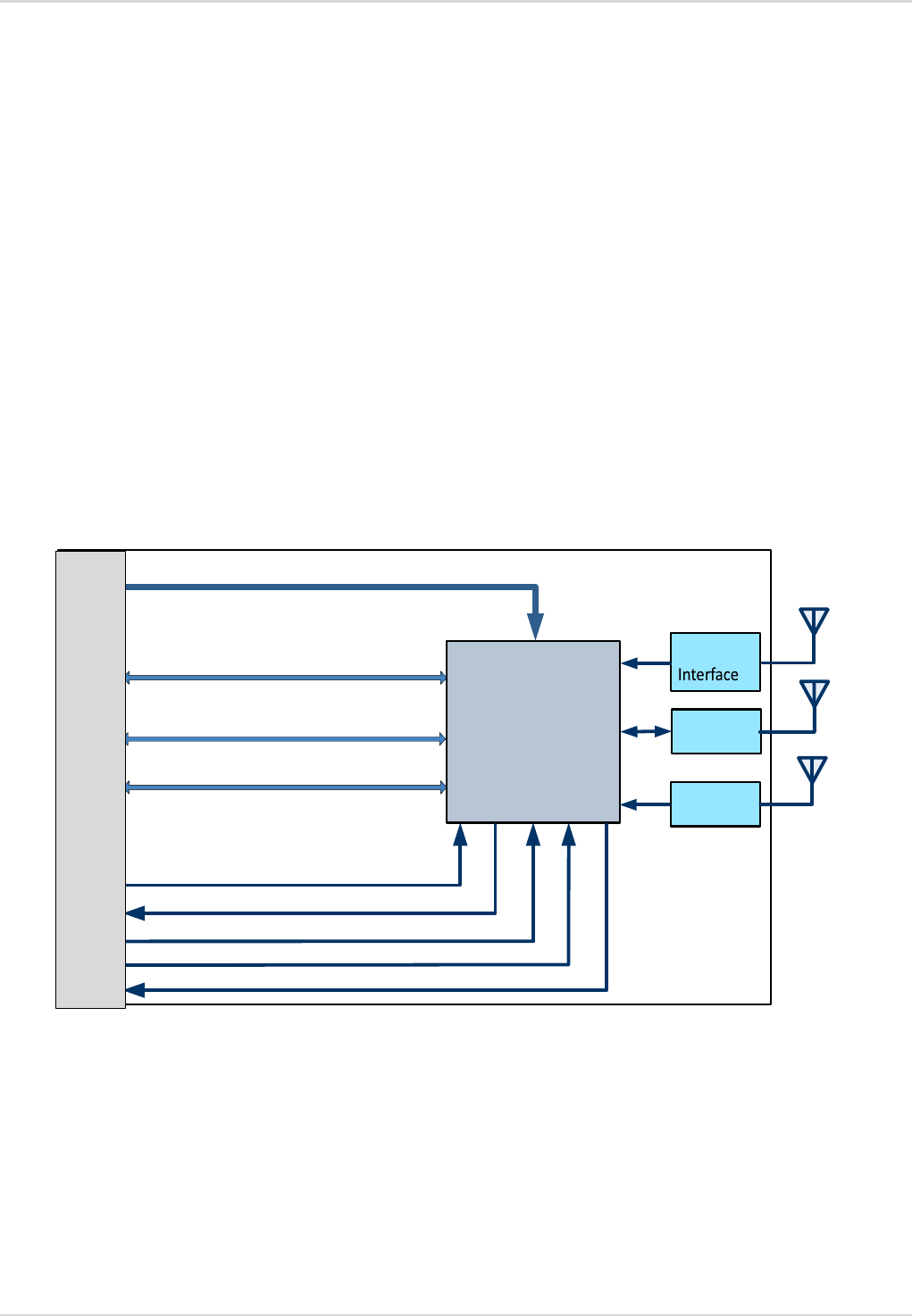
Figure 1 shows the functional diagram of the M2 module. The major functions are following:
Support line 1 of USIM card interface
Support line 1 of USIM 2.0 interface
Support line 1 of UART interface
Support LED status indication
Support RF shut-down feature
Support external reset feature
Support sleep control and sleep indication
Support 3 RF antenna interfaces
Figure 1 Functional Diagram
uCloudlink
M2
Mini
PCIe-C
UART
USB
W_DISABLE#
PERST#
LED_WWAN#
Antenna
Interface
VBAT
USIM
WAKEUP_OUT
WAKEUP_IN
Mini PCI Express Interface
Antenna
Interface
Main
Antenna
Diversity
Antenna
Antenna
WIFI BT
Antenna

uCloudlink M2 Mini PCIe-C _Hardware Design Guide_V1.0
14/35
3 Interface Application
3.1 About This Chapter
This chapter mainly gives the external application interfaces of the M2 module, including:
Power Interface
UART Interface
USIM Interface
USB Interface
Control Signal
Antenna Interface
3.2 M2 Module Interface
3.2.1 Interface Definition
The interface of the M2 module is the standard Mini PCI Express interface. For details about
the 52-pin interfaces, see table 3 I/O parameters definition.
Table 3 Definition of I/O parameters
Mark Description
IO Bidirectional input/output
DI Digital Input
DO Digital Output
AI Analog Input

uCloudlink M2 Mini PCIe-C _Hardware Design Guide_V1.0
15/35
AO Analog Output
PI Power Input
PO Power Output
OC Open Collector
Table 4 Definition of pins on the M2 module
Pin No. Status Pin Name I/O Description Note
1 WAKE# MIC_P* AI
Audio
Input(Positive)
2 3.3Vaux VBAT PI Power Input
3 COEX1 MIC_N* AI
Audio
Input(Negative)
4 GND GND Ground
5 COEX2 SPK_P* AO
Audio
Output(Positive)
6 1.5V NC — —
7 CLKREQ# SPK_N* AO
Audio
Output(Negative)
8 UIM_PWR USIM_VDD PO
USIM Power
Output
9 GND GND Ground
10 UIM_DATA USIM_DATA IO USIM data signal
11 REFCLK- VDD_EXT PO 1.8V Power Output

uCloudlink M2 Mini PCIe-C _Hardware Design Guide_V1.0
16/35
12 UIM_CLK USIM_CLK DO USIM Clock Signal
13 REFCLK+ RESERVED — Reserved
14 UIM_RESET USIM_RST DO USIM Reset Signal
15 GND GND Ground
16 UIM_VPP RESERVED — Reserved
17 RESERVED RESERVED — Reserved
18 GND GND Ground
19 RESERVED WAKEUP_IN DI
Module Sleep
Control Pin
Allows to
sleep when
low level
20 W_DISABLE# W_DISABLE# DI
Disable RF
Communication
Valid when
low level
21 GND GND Ground
22 PERST# PERST# DI Reset Control Pin
Valid when
low level
23 PERn0 UART_RXD DI
Module receiving
end
24 3.3Vaux VBAT PI Power Input
25 PERp0 UART_RTS DO
Module request
to send
26 GND GND Ground
27 GND GND Ground
28 1.5V UART_CTS DI
Module request
to delete

uCloudlink M2 Mini PCIe-C _Hardware Design Guide_V1.0
17/35
29 GND GND Ground
30 SMB_CLK UART_DCD DO
Module Carrier
Sense
31 PETn0 UART_TXD DO
Module sending
end
32 SMB_DATA WAKEUP_OUT DO
Module Sleep
Indication
33 PETp0 PERST# DI Reset Control Pin
Valid when
low level
34 GND GND Ground
35 GND GND Ground
36 USB_D- USB_DM IO USB Differential Signal (-)
37 GND GND Ground
38 USB_D+ USB_DP IO USB Differential Signal (+)
39 3.3Vaux VBAT PI Power Input
40 GND GND Ground
41 3.3Vaux VBAT PI Power Input
42 LED_WWAN# LED_WWAN# OC Status Light Indication
43 GND GND Ground
44 LED_WLAN# RESERVED — Reserved
45 RESERVED RESERVED — Reserved
46 LED_WPAN# UART_DTR DI DTE is ready
47 RESERVED RESERVED — Reserved
48 1.5V NC — —
49 RESERVED RESERVED — Reserved
50 GND GND Ground
51 RESERVED RESERVED — Reserved
uCloudlink M2 Mini PCIe-C _Hardware Design Guide_V1.0
18/35
52 3.3Vaux VBAT PI Power Input
Note
1
Besides USIM interfaces, the voltage domain of other digital interfaces is 1.8V, and the
USIM interface is available with 1.8V and 3.0V.
2. Please suspend all of NC, RESERVED and unused pins.
3. “*” indicates the audio feature is not available and reserved function.
3.2.2 Pin Assignment
The following figure shows the pin assignment of the M2 module, and the top face is for sticking
antenna connector and opposite face is the BOT.
Figure 2 Pin Assignment (Top View)
uCloudlink M2 Mini PCIe-C _Hardware Design Guide_V1.0
19/35
3.3 Power Interface
Table 5 lists the definitions of the pins on the power supply interface.
Table 5 Definition of power interfaces
Pin No. Pin Name I/O Description
2, 24, 39 , 41, 52 VBAT PI 3.3~3.6V Power Input
4, 9, 15, 18, 21,
26, 27, 29, 34 ,35,
37, 40, 43, 50
GND
Ground
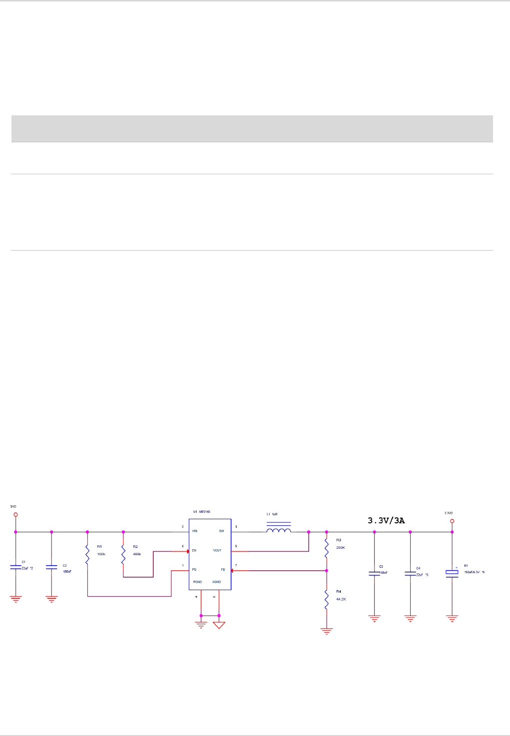
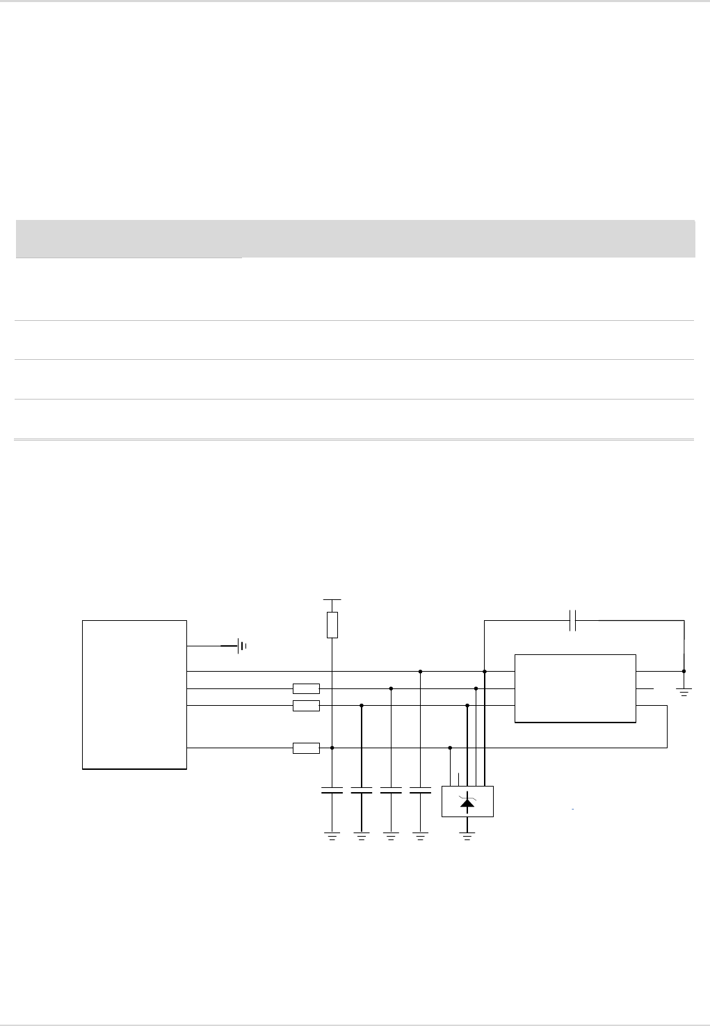
When the M2 module works normally, power is supplied through the VBAT pins. When it works
at EGSM900 mode and transmits current may reach the transient peak value of about 2.5 A. To make
sure that the voltage does not decrease below 3.3V, a low-dropout (LDO) regulator or switch power
with current output of more than 2.5 A is recommended for external power supply. Furthermore, it is
recommended that customers add the 1000uF or above energy storage capacitor to connect in
parallel at the power interface of the M2 module. And keep the power device and power cable away
from antenna to avoid EMI interference.
Figure 3 shows the recommended power circuit of M2 module using DC-DC power supply. The
resistance accuracy of R3 and R4 is 1%. The capacitance E1 needs to use high polymer tantalum
capacitor to add the drive capability of pulse current in dialing process.
Figure 3 Recommended Power Circuit of the M2 module
uCloudlink M2 Mini PCIe-C _Hardware Design Guide_V1.0
20/35
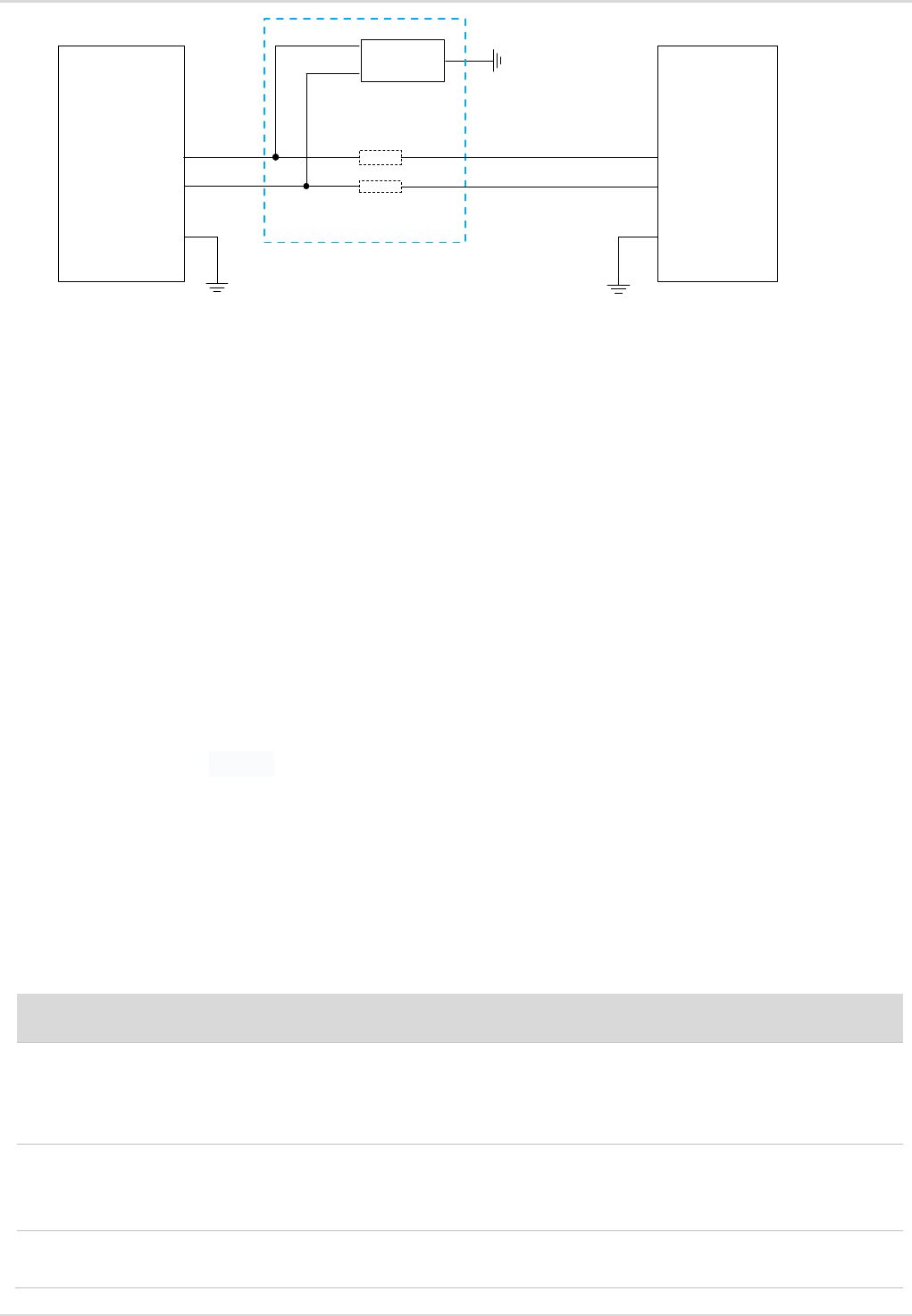
3.4 UART Interface
Table 6 lists the UART interface signals.
Table 6 UART interface signals
Pin No. Pin name I/O Typ.(V) Description
23 UART_RXD DI 1.8V Receive data
31 UART_TXD DO 1.8V Send data
28 UART_CTS DI 1.8V Clear to Send
25 UART_RTS DO 1.8V Ready for Receive
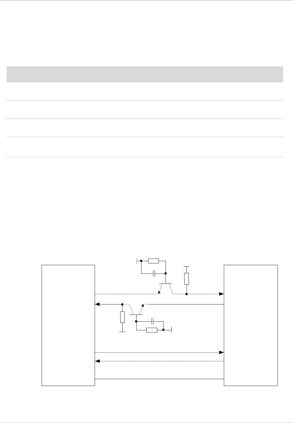
The M2 module is available with 1-wire hardware flow control UART (DSR and R1 signal are not
supported), which supports 9600, 19200, 38400, 57600, 115200, 230400bps and the default value is
115200bps.
Figure 4 shows the recommended power circuit of level match in the 3.3V power. Pay attention
to the connection direction. The dotted circuit and full circuit can be used as reference to each other.
Figure 4 Recommended Power Circuit of Level Match
MCU/ARM
/TXD
/RXD
VDD_EXT
10 K
VCC_MCU 4.7 K
K 10
VDD_EXT
UART_TXD
UART_RXD
UART_RTS
UART_CTS
/RTS
/CTS
GND
Module
VDD_EXT 4.7 K
GND
1 nF
1 nF
Voltage level: 3.3V
-
uCloudlink M2 Mini PCIe-C _Hardware Design Guide_V1.0
21/35
3.5 USIM Card Interface
The signal definition of the M2 module USIM card interface is as below.
Table 7 USIM card interface signals
Pin No. Pin Name I/O Typ.(V) Description
8 USIM_VDD PO 1.8V/3.0V Output Power supply for
USIM card
10 USIM_DATA IO 1.8V/3.0V USIM/SIM Data
12 USIM_CLK DO 1.8V/3.0V USIM/SIM Clock
14 USIM_RST DO 1.8V/3.0V USIM/SIM Reset
The M2 module is available with 1.8V and 3.0V USIM/SIM card.
Figure 5 shows the circuit of the 6-pin USIM card interface.
Figure 5 Circuit of the 6-pin USIM Card Interface
USIM_VDD
GND
USIM_RST
USIM_CLK
USIM_DATA 22 R
22 R
22 R
100 nF
USIM 卡座
GND
ESD
33 pF33pF33pF
VCC
RST
CLK IO
VPP
GND
GND
100 nF
15 K
Module
USIM_VDD

uCloudlink M2 Mini PCIe-C _Hardware Design Guide_V1.0
22/35
In order to enhance the reliability and availability of the USIM card, please pay attention to
these key points:
1. The USIM socket should be placed near the USIM interface and it is recommend that PCB
circuit connecting the USIM interface to the USIM socket does not exceed 200 mm.
2. Keep USIM card signal cable away from RF antenna and module power cable.
3. The decouple capacitor of USIM_VDD should be less than 1uF and placed near the USIM socket.
4. To avoid the mutual interference between USIM_DATA and USIM_CLK, keep them away with
each other and shield them with surrounded ground including USIM_RST.
5. In order to ensure ESD protection in good performance, it is recommended to place the TVS
with stray capacitance of less than 50pF near USIM card socket.
6. It is recommended to connect the 22Ω resistors to USIM_CLK, USIM_DATA and USIM_RST to
avoid EMI interference and enhance ESD protection. Meanwhile, connecting the 33pF
capacitor in parallel to filter interference from EGSM900 RF signals, and keep these
components close to the USIM card socket.
7. USIM_DATA is pulled up internally, which is good for improving the anti-jamming capability.
When the PCB circuit of USIM card is too long or the interference is nearby, the pull-up resistor
is recommended to be placed close to the USIM socket.
3.6 USB Interface
The Pin definition of the M2 module USB interface is as below.
Table 8 Definition of the USB interface
Pin No. Pin Name Pad Type Description Comment
36 USB_DM IO
USB differential data
bus(minus)
Require differential
impedance of 90ohm
38 USB_DP IO
USB differential data
bus(positive)
Require differential
impedance of 90ohm
The M2 module is compliant with USB 2.0 High Speed Mode (480Mbps) and Full Speed Mode
12Mbps). And only can be used as slave device. The USB interface is mainly for AT commands, data
Figure 6 shows the circuit of the USB interface
transfer, catch log, and software upgrade.
uCloudlink M2 Mini PCIe-C _Hardware Design Guide_V1.0
23/35
Figure 6 Recommended Circuit of USB Interface
In order to meet the requirement for completeness of USB signal trace, R1 and R2 shall be placed
near the M2 module and ESD protection components.
Based on the USB 2.0 specification, please comply with the following requirements:
1. It is required to control the differential impendence -90ohm.
2. Do not route the USB signal trace under the following components: crystals, oscillator,
electromagnetic component and RF signal. Keep it away from interference sources and signals
susceptible to disturbance and shielding with ground.
3. If the USB interface of the M2 module is connected to the USB socket, place ESD protection
component with no more than of 2pF capacitance near the USB socket.
4. Avoid the coupled noise on the USB signal trace, keep the testing stubs as short as possible. If
possible, add resistor of 0 ohm or common mode choke to the USB signal trace.
3.7 Signal Control Signal
Table 9 lists the pins on the signal control interface.
Table 9 Definition of the pins on the signal control interface
Pin No. Pin Name Pad Type Typ.(V) Description
20 W_DISABLE# DI 1.8V
Disable RF communication, effective
low level (inside pull up)
22, 33 PERST# DI 1.8V
Reset control, low level reset (internal
pull up)
42 LED_WWAN# OC — Status Indication
USB_DP
USB_DM
GND
USB_DP
USB_DM
GND
R1
R2
Close to Module
ESD Array
R 0
0 R
Module MCU
uCloudlink M2 Mini PCIe-C _Hardware Design Guide_V1.0
24/35
19 WAKEUP_IN DI 1.8V Sleep control pin (internal pull-down)
32 WAKEUP_OUT DO 1.8V Sleep indication
3.7.1 W_DISABLE# Signal
The W_DISABLE# signal can be used to disable the RF communication
,
which can controlled through hardware and software. Table 10 shows the operating status of
radio frequency.
Table 10 Operating status of radio frequency
W_DISABLE# RF status
High Level Enable RF
High Level Disable RF
Low Level Disable RF
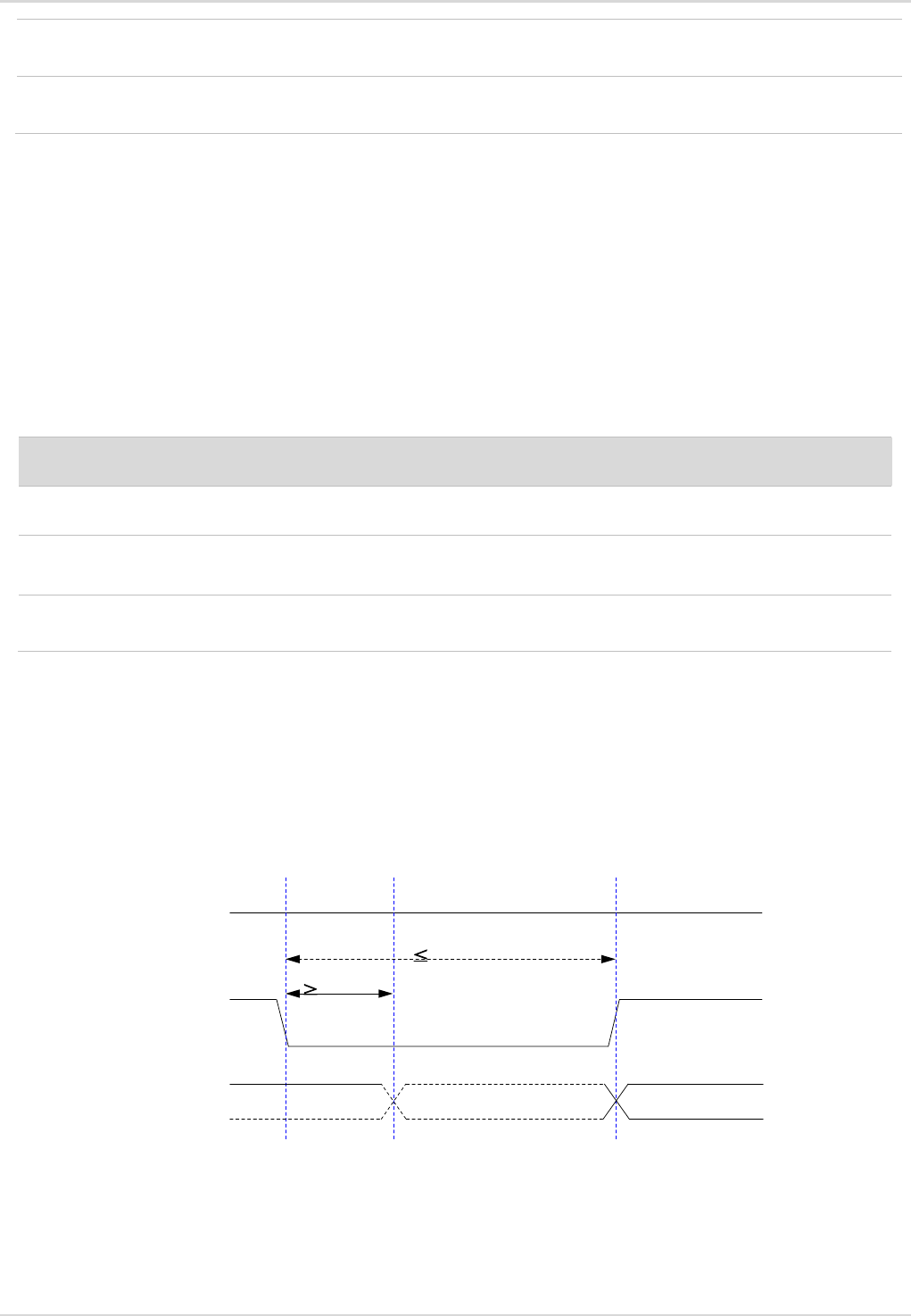
3.7.2 PERST# Signal
PERST# signal can be used externally reset the module. PERST# 150~460ms can be pulled
down to reset the module. PERST# signal is sensitive to interference, so keep the route on the
module interface board as short as possible and shield with ground.
Figure 7 Timing Sequence of Module Reset
V
IL
≤ 0.5V
V IH ≥ 1.3V
VBAT
ms 150
Resetting
Module
Status
Running
PERST#
Restart
460 ms

uCloudlink M2 Mini PCIe-C _Hardware Design Guide_V1.0
25/35
3.7.3 LED_WWAN# Signal
The LED_WWAN# signal interface is OC output format and the max current can reach up to the
40mA. When it connects to LED externally, connects the resistor in serial. You can adjust the LED
brightness by adjusting the resistance of resistor. When it is low, the external LED lights up.
Figure 8 shows the recommended circuit of the LED_WWAN# pin.
VCC
Figure 8 Driving Circuit
Check the LED_WWAN# signal network status indicator as below, when the M2 module is
successfully registered, the LED is on. When the RF is disabled, turned off or error (No SIM card
or registration failed), the LED is off.
Table 11 Network status indication
LED_WWAN# Description
Low Level(LED is on) Successfully registered
High Impedance(LED is off)
1. No Internet or registration failed
1. W_DISABLE# pin is pulled down(disable RF)
3.7.4 WAKEUP_IN and WAKEUP_OUT Signal
WAKEUP_IN pin is the authorization signal of the M2 module entering sleep mode. WAKEUP_OUT
pin is used to wake up the external devices.
Table 12 shows the definition of the WAKEUP_IN pin and WAKEUP_OUT signal.
Table 12 WAKEUP_IN and WAKEUP_OUT pin
Pin Name Description
WAKEUP_IN
H: DTE Wake up Module
L: DTE Allows to enable sleep mode
LED_WWAN# R
uCloudlink M2 Mini PCIe-C _Hardware Design Guide_V1.0
26/35
WAKEUP_OUT
H: Wake-up mode is on, USB and serial port are available
L: Wake-up is on, USB and serial port are not available
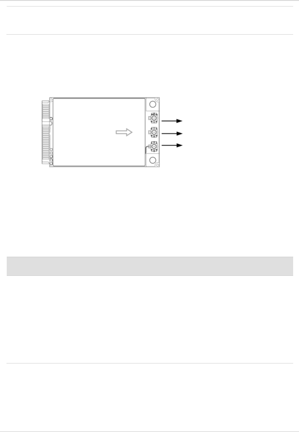
3.8 Antenna Interface
The M2 module provides three antenna pads (WIFI BT antenna pad, main antenna pad and DIV
antenna pad) for connecting the external antennas.
Figure 9 Antenna Interface
3.8.1 Antenna Requirements
Table 13 lists the requirements for main antenna, diversity antenna and WIFI/BT antenna.
Table 13 Antenna requirements
Type Requirements
Frequency range:
1575.42MHz
Polarization: RHCP or linear
VSWR: < 2 (Typ.)
VSWR: ≤ 2
WIFI BT Antenna Interface
Main Antenna Interface
DIV Antenna Interface
WIFI/BT/GPS
GPS
WIFI Frequency range:2412 - 2472Hz
BT Frequency range:2402 - 2482Hz
Passive antenna gain: > 0dBi
Passive antenna gain: > 0dBi
Gain (dBi): 1

uCloudlink M2 Mini PCIe-C _Hardware Design Guide_V1.0
27/35
GSM/
WCDMA/
TD-SCDMA/
LTE
Max input power (W): 50
Input resistance(ohm): 50
Polarization type: vertical
Cable insertion loss: < 1dB
(GSM900, WCDMA B8, LTE B8)
Cable insertion loss: < 1.5dB
Cable insertion loss: < 2dB
4 Electrical Interface and RF Specifications
4.1 About This Chapter
This chapter describes the mainly gives the electrical interface and RF specifications of the M2
module, including:
Power Supply Ratings
IO Interface
Working Current
RF Performance
WIFI/BT Receiving Sensitivity
ESD Feature
4.2 Power Supply Ratings
M2 module comes with VBAT voltage with the input voltage 3.3~3.6V and the input power at
least meets the requirement of 2.3A capacity. Table shows the power range of the M2 module.
Table 14 Input Power Range
Parameter Description Min. Typ. Max. Unit

uCloudlink M2 Mini PCIe-C _Hardware Design Guide_V1.0
28/35
VBAT
Module power
supply
3.3
3.6 V
4.3 I/O Interface
Table 15 shows the I/O interface of the M2 module.
Table 15 I/O Interface
Parameter Description Min. Max. Unit
VIH High Level Input Voltage 0.7*VDDIO1) VDDIO1)+0.3 V
VIL Low Level Input Voltage -0.3 0.3*VDDIO1) V
VOH High Level Input Voltage VDDIO1)-0.5 VDDIO1) V
VOL
Notes
Low Level Input Voltage 0 0.4 V
1. The voltage of PERST# and W_DISABLE VIL(max) is 0.5V.
2. VDDIO voltage is 1.8V
4.4 RF Specifications
Table 16 shows the RF output power and RF receiving sensitivity of the M2 module.
Table 16 RF Output Power
Band Max Min
GSM900 33dBm±2dB 5dBm±5dB
DCS1800 30dBm±2dB 0dBm±5dB
GSM900 (8-PSK) 27dBm±3dB 5dBm±5dB
DCS1800 (8-PSK) 26dBm±3dB 0dBm±5dB
WCDMA B1/B8 24dBm+1/-3dB <-49dBm

uCloudlink M2 Mini PCIe-C _Hardware Design Guide_V1.0
29/35
LTE FDD B1/B3/B8 23dBm±2dB <-39dBm
LTE TDD B38/B39/B40/B41 23dBm±2dB <-39dBm
Table 17 RF Receiving Sensitivity
Band
Receiving
Sensitivity(Typ.)
Master set
+Diversity 3GPP(Main+Diversity)
EGSM900 -109dBm NA NA -102dBm
DCS1800 -109dBm NA NA -102dBm
WCDMA Band1 -110dBm NA NA -106.7dBm
WCDMA Band8 -110dBm NA NA -103.7dBm
LTE-FDD B1(10M) -97dBm -97dBm -101dBm -96.3dBm
LTE-FDD B3(10M) -95dBm -94dBm -96dBm -93.3dBm
LTE-FDD B8(10M) -94dBm -94dBm -97dBm -93.3dBm
LTE-TDD B38(10M) -97dBm -97dBm -97.5dBm -96.3dBm
LTE-TDD B39(10M) -97dBm -97dBm -102dBm -96.3dBm
LTE-TDD B40(10M) -97dBm -97dBm -100dBm -96.3dBm
LTE-TDD B41(10M) -96dBm -96dBm -98dBm -94.3dBm
4.5 WIFI BT Receiving Sensitivity

uCloudlink M2 Mini PCIe-C _Hardware Design Guide_V1.0
30/35
The WIFI/BT receiver is disabled by default. As the WIFI/BT antenna interface connects to the power
2.95V, it is recommended to use the active antenna suitable for the voltage.
4.6 Electrostatic Discharge Characteristics
Table 18 lists the ESD (Electrostatic Discharge) characteristics of the M2 module.
Table 18 Electrostatics discharge characteristics
Parameter Contact Discharge Air Discharge Unit
Power and grounding
interface
+/-5 +/-10 kV
Antenna Interface +/-4 +/-8 kV
USB Interface +/-4 +/-8 kV
USIM Card Interface +/-4 +/-8 kV
Other Interface s +/-0.5 +/-1 kV
uCloudlink M2 Mini PCIe-C _Hardware Design Guide_V1.0
31/35
5 Mechanical Dimensions
This chapter gives the mechanical dimensions of the M2 module, including:
Outer Dimension of the M2 module
Standard dimension of Mini PCI Express
5.1. Outer Dimension of M2 Module
Figure 10 Outer Dimension of M2 Module (Unit: mm)
5.2. Standard Dimension
The M2 module comes with standard interfaces.
uCloudlink M2 Mini PCIe-C _Hardware Design Guide_V1.0
32/35
Figure 11 Standard Dimension of Mini PCI Express (Unit: mm)
Any qualified PCI Express Mini Card connectors are compatible with the M2 module. Figure 12
shows the connector 679100002 made of Molex Company.
Figure 12 Mini PCI Express Connector (Unit: mm)

uCloudlink M2 Mini PCIe-C _Hardware Design Guide_V1.0
33/35
6 Appendix Terms and Abbreviation
Table 19 Terms and Abbreviation
Abbr. Description
8-PSK 8-Phase Shift Keying
bps Bits Per Second
CS Coding Scheme
CSD Circuit Switched Data
CTS Clear To Send
DCE Data Communications Equipment (typically module)
DL Down Link
DTE Data Terminal Equipment (typically computer, external controller)
DTR Data Terminal Ready
EMC Electromagnetic Compatibility
ESD Electrostatic Discharge
FDD Frequency Division Duplexing
GLONASS
GLObalnayaNAvigatsionnayaSputnikovaya Sistema, the Russian Global
Navigation Satellite System
GMSK Gaussian Minimum Shift Keying
GNSS Global Navigation Satellite System
GPS Global Positioning System
GSM Global System for Mobile Communications
HSPA High Speed Packet Access

uCloudlink M2 Mini PCIe-C _Hardware Design Guide_V1.0
34/35
PAD TYPE Input/Output
kbps KiloBitsPer Second
LED Light Emitting Diode
LTE Long Term Evolution
Mbps Million Bits Per Second
MCS Modulation and Coding Scheme
ME Mobile Equipment
MMS Multimedia Messaging Service
MO Mobile Originated
MS Mobile Station (GSM engine)
MT Mobile Terminated
PAP Password Authentication Protocol
PDU Protocol Data Unit
PPP Point-to-Point Protocol
RF Radio Frequency
RX Receive Direction
SIM Subscriber Identification Module
SMS Short Message Service
TDD Time Division Duplexing
TD-SCDMA Time Division-Synchronous Code Division Multiple Access
TE Terminal Equipment
TTFF Time to First Fix
TX Transmitting Direction
UART Universal Asynchronous Receiver & Transmitter
UL Up Link
UMTS Universal Mobile Telecommunications System

uCloudlink M2 Mini PCIe-C _Hardware Design Guide_V1.0
35/35
URC Unsolicited Result Code
USSD Unstructured Supplementary Service Data
WCDMA Wideband Code Division Multiple Access
This device complies with Part 15 of the FCC Rules. Operation is subject to the following two
conditions: (1) this device may not cause harmful interference, and (2) this device must accept any
interference received, including interference that may cause undesired operation. Changes or
modifications not expressly approved by the party responsible for compliance could void the user's
authority to operate the equipment.
FCC Statement
NOTICE:
Please notice that if the FCC identification number is not visible when the module is installed inside
another device, then the outside of the device into which the module is installed must also display a
label referring to the enclosed module. This exterior label can use wording such as the following:
“Contains FCC ID:2AC88-GLMM18A02” any similar wording that expresses the same meaning may
be used.
This equipment complies with FCC radiation exposure limits set forth for an uncontrolled environment.
This equipment should be installed and operated with a minimum distance of 20cm between the
radiator & your body. This transmitter must not be co-located or operating in conjunction with any
other antenna or transmitter.
The module is limited to OEM installation ONLY.
The OEM integrator is responsible for ensuring that the end-user has no manual instruction
to remove or install module.
The module is limited to installation in mobile application.
A separate approval is required for all other operating configurations, including portable configurations
with respect to Part 2.1093 and difference antenna configurations.
There is requirement that the grantee provide guidance to the host manufacturer for compliance with
Part 15B requirements.
The finished product is required to comply with all applicable FCC equipment authorisations, regulati-
ons and qequipment. We will provide guidance to the host manufacturer for conpliance with the FCC
part 15B requiremnets.
The OEM integrator is responsible for ensuring that the end-user has no manual instructions to rem-
ove or install module.
The module is limited to installation in mobile or fixed application.