USA Alo Branch DR-235T VHF Scanning Receiver User Manual 2000437 FCC
USA Alinco Branch VHF Scanning Receiver 2000437 FCC
Manual
DR-235㨀㨀 Manual

NOTICE
This equipment has been tested and found to comply with the limits for a Class B digital device,
pursuant to part 15 of the FCC Rules.
These limits are designed to provide reasonable protection against harmful interference in a residential
installation. This equipment generates, uses, and can radiate radio frequency energy and, if not installed
and used in accordance with the instruction manual, may cause harmful interference to radio communi-
cations. However, there is no guarantee that interference will not occur in a particular installation. If
this equipment does cause harmful interference to radio or television reception, which can be deter-
mined by turning the equipment off and on, the user is encouraged to try to correct the interference by
one or more of the following measures:
• Reorient or relocate the receiving antenna.
• Increase the separation between the equipment and receiver.
• Connect the equipment into an outlet on a circuit different from that to which the receiver is con-
nected.
• Consult the dealer or an experienced radio/TV technician for help.
Tested to Comply
With FCC Standards
FOR HOME OR OFFICE USE
Information in this document is subject to change without notice or obligation. All brand names and
trademarks are the property of their respective owners. Alinco cannot be liable for pictorial or typo-
graphical inaccuracies. Some parts, options and/or accessories are unavailable in certain areas. Changes
or modifications not expressly approved by the party responsible for compliance could void the user's
authority to operate the equipment.
Copyright @ 2000 All rights reserved. No part of this document may be reproduced, copied, translated
or transcribed in any form or by any means without the prior written permission of Alinco. Inc., Osaka,
Japan. English Edition Printed in Japan.
5522''%%++((++%%##66++110055&46
عع))GGPPGGTTCCNN
(TGSWGPE[EQXGTCIG 㨪/*\4:
㨪/*\6:
1RGTCVKPIOQFG -('9KFGOQFG-('0CTTQYOQFG
(TGSWGPE[TGUQNWVKQP 㧘㧘㧘㧘㧘㧘㧘㧘
0WODGTQHOGOQT[EJCPPGNU
#PVGPPCKORGFCPEG ǡWPDCNCPEGF
2QYGTTGSWKTGOGPV 8&%rVQ8
)TQWPFOGVJQF 0GICVKXGITQWPF
4GEGKXG #/CZޓޓ#5SWGNEJGF%WTTGPVFTCKP
6TCPUOKV #
1RGTCVKPIVGORGTCVWTG ͠VQ͠
(TGSWGPE[UVCDKNKV[ rRRO
&KOGPUKQPU YJFOO
OOHQTRTQLGEVKQPKPENWFGF
9GKIJV #RRTQZMI
عع66TTCCPPUUOOKKVVVVGGTT
1WVRWVRQYGT *KIJ9
/KF9.QY9
/QFWNCVKQPU[UVGO 8CTKCDNGTGCEVCPEGHTGSWGPE[OQFWNCVKQP
/CZKOWOHTGSWGPE[FGXKCVKQP rM*\9KFGOQFGrM*\0CTTQYOQFG
5RWTKQWUGOKUUKQP F$
#FLCEGPVEJCPPGNRQYGT F$
0QKUGCPFJWOTCVKQ F$9KFGOQFGF$0CTTQYOQFG
/KETQRJQPGKORGFCPEG Mǡ
عع44GGEEGGKKXXGGTT
5GPUKVKXKV[ F$WHQTF$5+0#&
4GEGKXGTEKTEWKVT[ &QWDNGEQPXGTUKQPUWRGTJGVGTQF[PG
+PVGTOGFKCVGHTGSWGPE[ UV/*\PFM*\
5SWGNEJUGPUKVKXKV[ F$W
#FLCEGPVEJCPPGNUGNGEVKXKV[ F$9KFGOQFGF$0CTTQYOQFG
+PVGTOQFWTCVKQPTGLGEVKQPTCVKQ F$
5RWTKQWUCPFKOCIGTGLGEVKQPTCVKQ F$
#WFKQQWVRWVRQYGT 9ǡ6*&
00QQVVGG##NNNNUURRGGEEKKHHKKEECCVVKKQQPPUUCCTTGGUUWWDDLLGGEEVVVVQQEEJJCCPPIIGGYYKKVVJJQQWWVVPPQQVVKKEEGGQQTTQQDDNNKKIICCVVKKQQPP
CIRCUIT DESCRIPTION
ޓޓDR-235
1) Receiver System
The receiver system is a double superheterodyne system with a 30.85 MHz first IF and a 455 kHz second
IF.
1. Front End
The received signal at any frequency in the 216.000MHz to 279.995MHz range is passed through the low-
pass filter (L116, L115, L114, L113, C204, C203, C202, C216 and C215) and tuning circuit (L105, L104
and D105, D104), and amplified by the RF amplifier (Q107). The signal from Q107 is then passed through
the tuning circuit (L103, L107, L102, and varicaps D103, D107 and D102) and converted into 30.85 MHz
by the mixer (Q106). The tuning circuit, which consists of L105, L104, varicaps D105 and D104, L103,
L107, L102, varicaps D103, D107 and D102, is controlled by the tracking voltage form the VCO. The
local signal from the VCO is passed through the buffer (Q112), and supplied to the source of the mixer
(Q106). The radio uses the lower side of the superheterodyne system.
2. IF Circuit
The mixer mixes the received signal with the local signal to obtain the sum of and difference between them.
The crystal filter (XF102, XF101) selects 30.85 MHz frequency from the results and eliminates the signals
of the unwanted frequencies. The first IF amplifier (Q105) then amplifies the signal of the selected
frequency.
3. Demodulator Circuit
After the signal is amplified by the first IF amplifier (Q105), it is input to pin 24 of the demodulator IC
(IC108). The second local signal of 30.395 MHz , which is oscillated by the internal oscillation circuit in
IC108 and crystal (X104), is input through pin 1 of IC108. Then, these two signals are mixed by the
internal mixer in IC108 and the result is converted into the second IF signal with a frequency of 455 kHz.
The second IF signal is output from pin 3 of IC108 to the ceramic filter (FL101 or FL102), where the
unwanted frequency band of that signal is eliminated, and the resulting signal is sent back to the IC108
through pins 5.
The second IF signal input via pin 5 is demodulated by the internal limiter amplifier and quadrature
detection circuit in IC108, and output as an audio signal through pin 12.
4. Audio Circuit
The audio signal from pin 12 of IC108 is amplified by the audio amplifier (IC104:A),and switched by the
signal switch IC (IC111) and then input it to the de-emphasis circuit.
and is compensated to the audio frequency characteristics in the de-emphasis circuit (R203, R207, R213,
R209, C191, C218, C217) and amplified by the AF amplifier (IC104:D). The signal is then input to volume
(VR1) . The adjusted signal is sent to the audio power amplifier (IC117) through pin 1 to drive the speaker.
5. Squelch Circuit
The detected output which is outputted from the pin 12 of IC108 is inputted to pin 19 of IC108 after it was
been amplified by IC104:A and it is outputted from pin 20 after the noise component was been eliminated
from the composed band pass filter in the built in amplifier of the IC, then the signal is rectified by D106
to convert into DC component. The adjusted voltage level at VR101 is delivered to the comparator of the
CPU.
The voltage is led to pin 2 of CPU and compared with the setting voltage. The squelch will open if the
input voltage is lower than the setting voltage.
During open squelch, pin 30 (SQC) of the CPU becomes "L" level, AF control signal is being controlled
and sounds is outputted from the speaker.)
6.AIR Band Reception㧔T only㧕
If it is made air band receiving mode, IF signal is demodulated by AM decoder of IC106,and is output
from pin13 as the AF signal.
7.WIDE/NARROW switching circuit
The 2nd IF 455 kHz signal which passes through filter FL101 (wide) and FL102 (narrow) during narrow,
changes its width using the width control switching IC103 and IC102.
2) Transmitter System
1. Modulator Circuit
The audio signal is converted to an electrical signal by the microphone, and input it to the microphone
amplifier (Q6). Amplified signal which passes through mic-mute control IC109 is adjusted to an
appropriate mic-volume by means of mic-gain adjust VR106.
IC114:AandB consists of two operational amplifiers; one amplifier (pins 1, 2, and 3) is composed of pre-
emphasis and IDC circuits and the other (pins 5, 6, and 7) is composed of a splatter filter. The maximum
frequency deviation is obtained by VR107. and input to the signal switch (IC113) (9600 bps packet signal
input switch) and input to the cathode of the varicap of the VCO, to change the electric capacity in the
oscillation circuit. This produces the frequency modulation.
2. Power Amplifier Circuit
The transmitted signal is oscillated by the VCO, amplified by the drive amplifier (IC112) and younger
amplifier (Q115), and input to the final power module (IC110). The signal is then amplified by the final
power module (IC110) and led to the antenna switch (D110) and low-pass filter (L113, L114, L115, L116,
C215, C216, C202, C203 and C204), where unwanted high harmonic waves are reduced as needed, and the
resulting signal is supplied to the antenna.
3. APC Circuit
Part of the transmission power from the low-pass filter is detected by D111 and D112, converted to DC.
The detection voltage is passed through the APC circuit (Q118, Q117, Q116), then it controls the APC
voltage supplied to the younger amplifier Q115 and the final power module IC110 to fix the transmission
power.
3) PLL Synthesizer Circuit
1. PLL
The dividing ratio is obtained by sending data from the CPU (IC1) to pin 2 and sending clock pulses to pin
3 of the PLL IC (IC501). The oscillated signal from the VCO is amplified by the buffer (Q504 and Q501)
and input to pin 15 of IC501. Each programmable divider in IC501 divides the frequency of the input
signal by N according to the frequency data, to generate a comparison frequency of 5 or 6.25 kHz.
2. Reference Frequency Circuit
The reference frequency appropriate for the channel steps is obtained by dividing the 12.8 MHz reference
oscillation (X103) by 2560 or 2048, according to the data from the CPU (IC1). When the resulting
frequency is 5 kHz, channel steps of 5, 10, 15, 20, 25, 30, and 50 kHz are used. When it is 6.25 kHz, the
12.5 kHz channel step is used.
3. Phase Comparator Circuit
The PLL (IC501) uses the reference frequency, 5 or 6.25kHz. The phase comparator in the IC501
compares the phase of the frequency from the VCO with that of the comparison frequency, 5 or 6.25kHz,
which is obtained by the internal divider in IC501.
4. PLL Loop Filter Circuit
If a phase difference is found in the phase comparison between the reference frequency and VCO output
frequency, the charge pump output (pin 13) of IC501 generates a pulse signal, which is converted to DC
voltage by the PLL loop filter and input to the varicap of the VCO unit for oscillation frequency control.
5. VCO Circuit A Colpitts oscillation circuit driven by Q503 directly oscillates the desired frequency. The
frequency control voltage determined in the CPU (IC1) and PLL circuit is input to the varicaps (D503 and
D504). This change the oscillation frequency, which is amplified by the VCO buffer (Q504) and output
from the VCO area.
4) CPU and Peripheral Circuits
1. LCD Display Circuit
The CPU turns ON the LCD via segment and common terminals with 1/4 the duty and 1/3 the bias, at the
frame frequency is 64Hz.
2. Dimmer Circuit
The dimmer circuit makes the output of pin 13 of CPU (IC1) into "H" level at set mode, so that Q9 and Q3
will turn ON to make the lamp control resistor R84 short and make its illumination bright. But on the other
hand, if the dimmer circuit makes pin 13 into "L" level, Q9 and Q3 will turn OFF, R84's illumination will
become dimmer as its hang on voltage falls down in the working LED (D11, D2, D5, D3 and D6).
3. Reset and Backup
When the power form the DC cable increases from Circuits 0 V to 2.5 or more, "H" level reset signal is
output form the reset IC (IC4) to pin 33 of the CPU (IC1), causing the CPU to reset. The reset signal,
however, waits at 100, and does not enter the CPU until the CPU clock (X1) has stabilized.
4. S(Signal) Meter Circuit
The DC potential of pin 16 of IC106 is input to pin 1 of the CPU (IC1), converted from an analog to a
digital signal, and displayed as the S-meter signal on the LCD.
5. DTMF Encoder
The CPU (IC1) is equipped with an internal DTMF encoder. The DTMF signal is output from pin 10,
through R35, R34 and R261 (for level adjustment), and then through the microphone amplifier (IC114:A),
and is sent to the varicap of the VCO for modulation. At the same time, the monitoring tone passes through
the AF circuit and is output form the speaker.
6. Tone Encoder
The CPU (IC1) is equipped with an internal tone encoder. The tone signal (67.0 to 250.3 Hz) is output
from pin 9 of the CPU to the varicap (D503 and D504) of the VCO for modulation.
㧲㧲㧾㧾㧻㧻㧺㧺㨀㨀ޓޓ㨂㨂㨕㨕㨑㨑㨣㨣
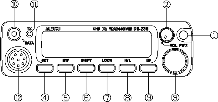
Primary Functions
Ԙ PWR Power turns ON/OFF whenever power supply switch is pressed.
ԙ Volume knob Adjusts the volume level.
Ԛ Dial Changes the frequency, memory channel and scan direction.
ԛ FUNC/SET Sets in the function mode to access additional setting.
Ԝ V/M/MWޓSwitches between VFO mode and memory mode.
ԝ MHZ/SHIFT Changes the frequency in 1 MHz steps.
Ԟ TSDCS/LOCK Sets the tone squelch and DCS setting.
ԟ CALL/H/L Switches to CALL mode.
Ԡ SQL/D Sets the squelch level
ԡ DATA Terminal Used in clone and burglar alarm functions.
Ԣ TX Light indicator Lights on during transmission.
ԣ Mic. Connector Connectino port for supplied microphone.
Functions which can be activated while F appears, after pressing the FUCN Key.
ԛFUNC/SETޓConfirms selection of other functions and exits the function mode.
ԜV/M/MWޓWrite in to memory channel.
ԝMHZ/SHIFTޓSets the shift setting and the offset frequency.
ԞTSDCS/LOCKޓSets the key lock function.
ԟCALL/H/LޓSwitches between HI, MID, and LOW power transmission.
ԠSQL/DޓAccesses the 9600 bps packet communication mode.
Functions that can be activated while pressing the FUNC Key
Ԙ PWR Reset to factry defalt settings.
ԜV/M/MWޓErase the memory.
ԝMHZ/SHIFTޓSwitches to wide / narrow mode reception.
ԞTSDCS/LOCKޓSets the auto dialer.
ԟCALL/H/LޓAccesses the clone function mode.
ԠSQL/DޓAccesses the power supply voltage indication mode.
Functions that requires continuous pressing to be activated.
ԛ FUNC/SETޓWhen press within 2 seconds, it accesses the set mode
Ԡ SQL/DޓWhen press within 1 second, the monitor function is on.
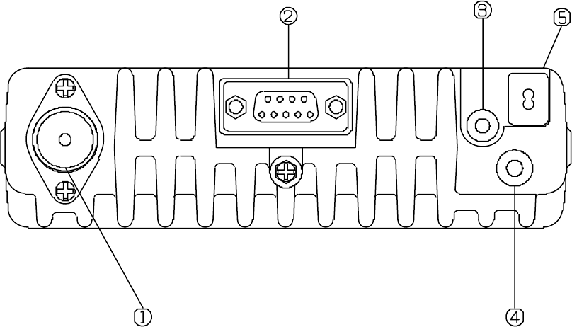
㧼㧼㧱㧱㧭㧭㧾㧾ޓޓ㨂㨂㨕㨕㨑㨑㨣㨣
Ԙ Antenna Connector
Connection for 50 ohm coaxial cable and antenna.
ԙ DSUB9 Connector
Terminal where external TNC may be connected for packet use.
With optional EJ-41U, connects internal TNC to the connector.
ԚExternal Speaker Terminal
Terminal for market available external speaker.
ԛExternal Power jack
Terminal for connecting optional EDC-37 for use with ignition key
on/off function.
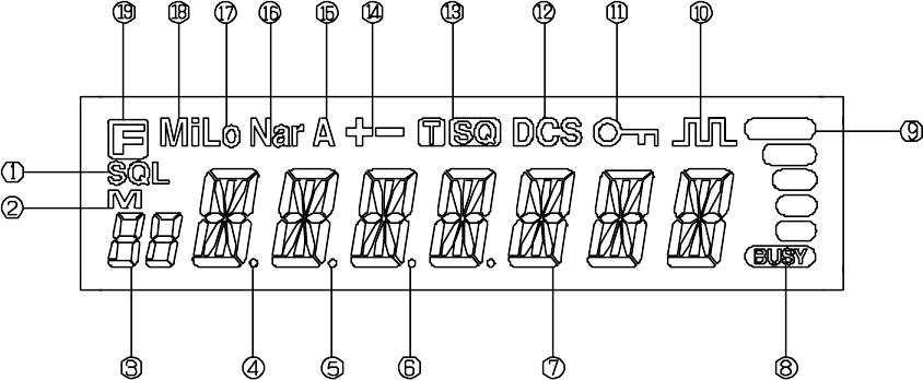
DISPLAY
ԘSQL Appears when setting the squelch level.
ԙM Appears when in memory mode
Ԛ88 Indicates the memory no. in memory mode
ԛ.Decimal point Appears when setting the burglar alarm function.
Ԝ. Decimal pointޓAppears when setting the decimal point of skip level.
ԝ. Decimal pointޓIndicates the decimal point of frequency and the scanning movement.
Ԟ8888888 Indicates the frequency and memory name
ԟBUSY Appears when signal is being receive.
ԠS-meter Indicates the signal strength level of transmission / reception.
ԡޓ Appears when in 9600 bps packet mode.
ԢޓޓAppears when setting the key lock.
ԣDCSޓAppears when setting the DCS.
ԤTSQ Appears when setting the tone squelch
ԥ㧗㧙 Appears when setting the shift.
ԦA Appears during AM reception.
ԧNar Appears when in narrow band reception mode
ԨLo Appears when transmission power is set to LOW㧚
ԩMi Appears when transmission power is set to MID
ԪF Appears when FUNC Key is pressed.
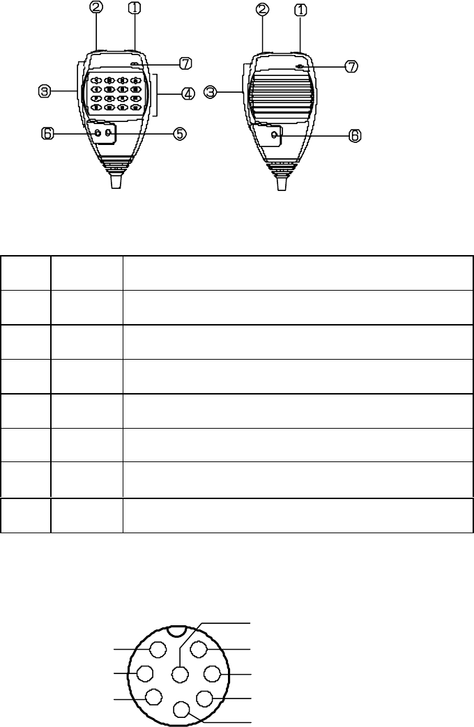
MICROPHONE
ޓޓޓޓޓޓޓޓDR-235TޓޓޓޓޓޓDR-235T (option)
No. Key Function
ԘUP Increase the frequency, memory channel number, or setting
value.
ԙDOWN Decrease the frequency, memory channel number, or setting
value.
ԚPTT Press the PTT(Push-To-Talk)key to transmit.
ԛDTMF DTMF tone keys.
ԜDTMF
ON/OFF Switches DTMF mic key illumination ON/OFF.
ԝLock
Switch Locks out the UP and DOWN keys.
ԞMIC Speak here during transmission.
Mic. Connector Diagram (While looking in the front view of the connector)
1((
.1 %-
& 6/(
1((
.1% -
1( (
&190
72
)0&
/+% )0&
&% 8
266
/+%
4'/16'