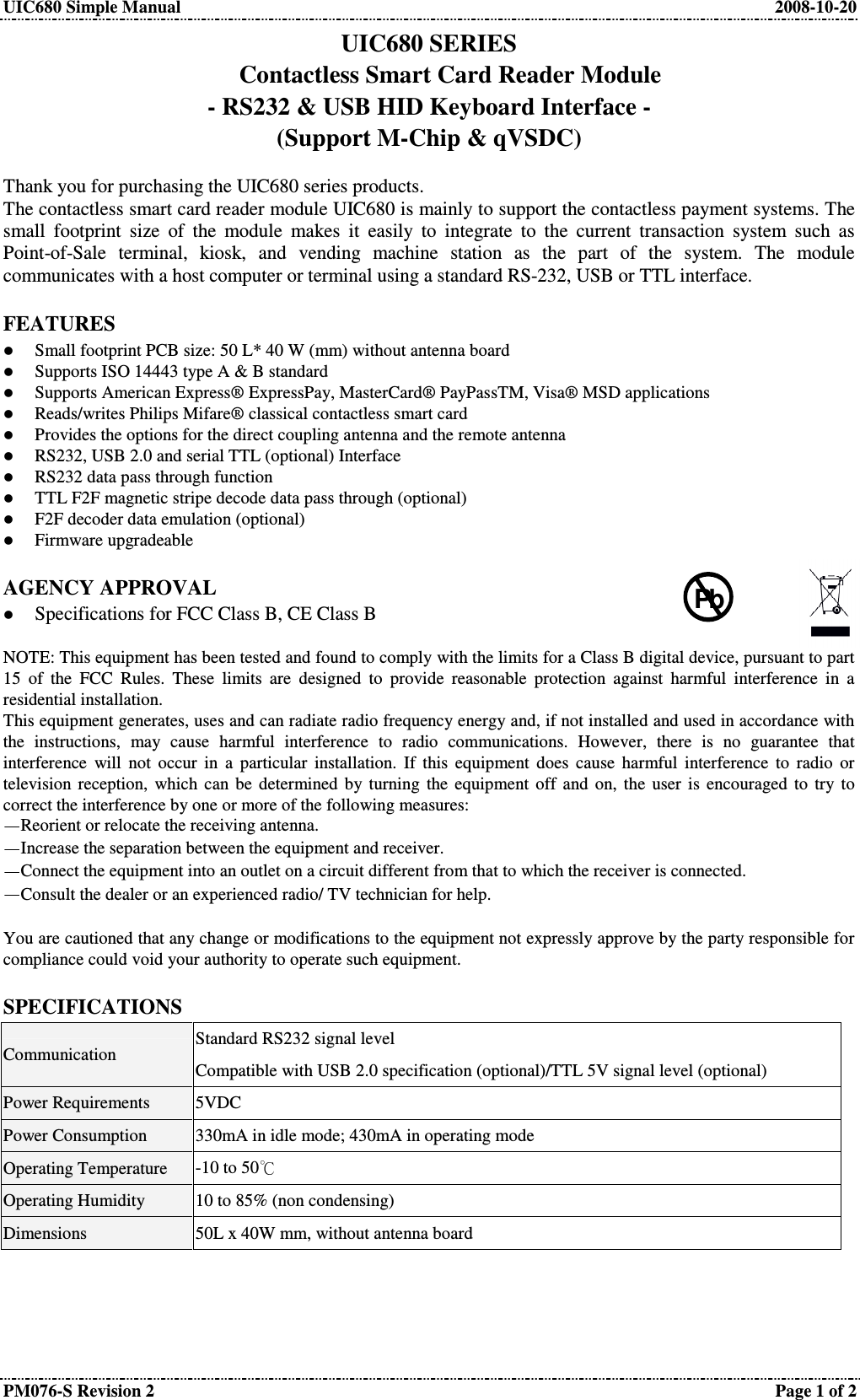
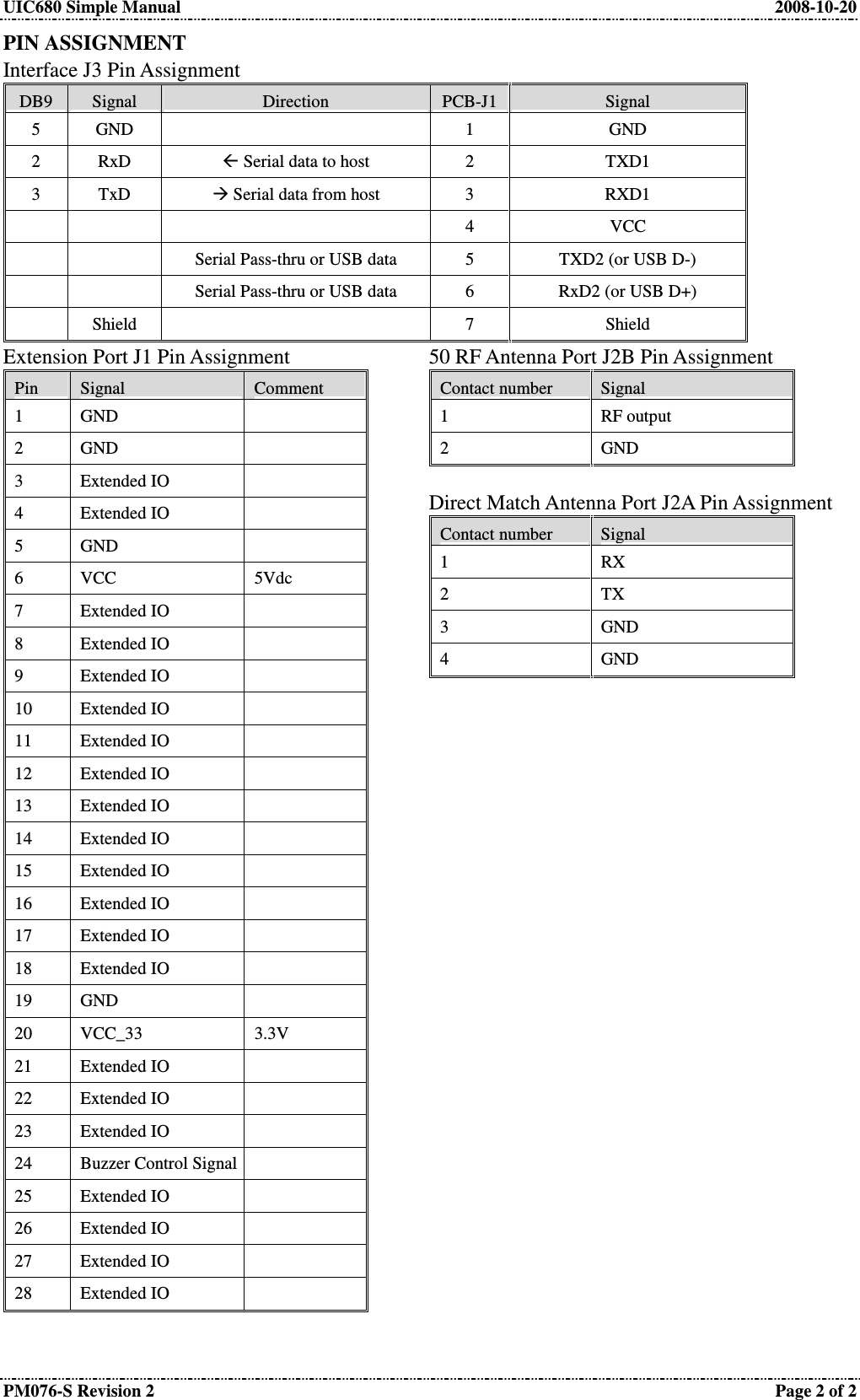
Uniform 680CLB Contactless Smart Card Reader Module User Manual

Uniform Industrial Corp. Contactless Smart Card Reader Module

User manual

UIC680 Simple Manual  2008-10-20 PM076-S Revision 2  Page 1 of 2 UIC680 SERIES Contactless Smart Card Reader Module - RS232 & USB HID Keyboard Interface - (Support M-Chip & qVSDC)  Thank you for purchasing the UIC680 series products. The contactless smart card reader module UIC680 is mainly to support the contactless payment systems. The small  footprint  size  of  the  module  makes  it  easily  to  integrate  to  the  current  transaction  system  such  as Point-of-Sale  terminal,  kiosk,  and  vending  machine  station  as  the  part  of  the  system.  The  module communicates with a host computer or terminal using a standard RS-232, USB or TTL interface.  FEATURES   Small footprint PCB size: 50 L* 40 W (mm) without antenna board   Supports ISO 14443 type A & B standard   Supports American Express® ExpressPay, MasterCard® PayPassTM, Visa® MSD applications   Reads/writes Philips Mifare® classical contactless smart card   Provides the options for the direct coupling antenna and the remote antenna   RS232, USB 2.0 and serial TTL (optional) Interface   RS232 data pass through function   TTL F2F magnetic stripe decode data pass through (optional)   F2F decoder data emulation (optional)   Firmware upgradeable  AGENCY APPROVAL   Specifications for FCC Class B, CE Class B  NOTE: This equipment has been tested and found to comply with the limits for a Class B digital device, pursuant to part 15  of  the  FCC  Rules.  These  limits  are  designed  to  provide  reasonable  protection  against  harmful  interference  in  a residential installation. This equipment generates, uses and can radiate radio frequency energy and, if not installed and used in accordance with the  instructions,  may  cause  harmful  interference  to  radio  communications.  However,  there  is  no  guarantee  that interference  will  not  occur  in  a  particular  installation.  If  this  equipment  does  cause  harmful  interference  to  radio  or television  reception,  which  can  be  determined  by  turning  the  equipment  off  and  on,  the  user  is  encouraged  to  try  to correct the interference by one or more of the following measures: Reorient or relocate the receiving antenna. Increase the separation between the equipment and receiver. Connect the equipment into an outlet on a circuit different from that to which the receiver is connected. Consult the dealer or an experienced radio/ TV technician for help.  You are cautioned that any change or modifications to the equipment not expressly approve by the party responsible for compliance could void your authority to operate such equipment.  SPECIFICATIONS Communication  Standard RS232 signal level Compatible with USB 2.0 specification (optional)/TTL 5V signal level (optional) Power Requirements  5VDC Power Consumption  330mA in idle mode; 430mA in operating mode Operating Temperature  -10 to 50  Operating Humidity  10 to 85% (non condensing) Dimensions  50L x 40W mm, without antenna board   Pb
UIC680 Simple Manual  2008-10-20 PM076-S Revision 2  Page 2 of 2 PIN ASSIGNMENT Interface J3 Pin Assignment DB9 Signal Direction PCB-J1 Signal 5  GND    1  GND 2  RxD   Serial data to host  2  TXD1 3  TxD   Serial data from host  3  RXD1       4  VCC     Serial Pass-thru or USB data  5  TXD2 (or USB D-)     Serial Pass-thru or USB data  6  RxD2 (or USB D+)   Shield    7  Shield  Extension Port J1 Pin Assignment Pin Signal Comment 1  GND   2  GND   3  Extended IO   4  Extended IO   5  GND   6  VCC  5Vdc 7  Extended IO   8  Extended IO   9  Extended IO   10  Extended IO   11  Extended IO   12  Extended IO   13  Extended IO   14  Extended IO   15  Extended IO   16  Extended IO   17  Extended IO   18  Extended IO   19  GND   20  VCC_33  3.3V 21  Extended IO   22  Extended IO   23  Extended IO   24  Buzzer Control Signal  25  Extended IO   26  Extended IO   27  Extended IO   28  Extended IO    50 RF Antenna Port J2B Pin Assignment Contact number Signal 1  RF output 2  GND  Direct Match Antenna Port J2A Pin Assignment Contact number Signal 1  RX 2  TX 3  GND 4  GND
 This device is intended for use under the following conditions:   1. The transmitter module may not be co-located with any other transmitter or antenna.  2. The module is approved using the FCC “unlicensed modular transmitter approval” method.   As long as these two conditions are met, further transmitter testing will not be required. However, the OEM integrator is still responsible for testing their end product for any additional compliance measures necessitated by the installation of this module (i.e. digital device emissions, PC peripheral requirements, etc.).   Note: In the event that these conditions cannot be met (i.e. co-location with another transmitter), then the FCC authorization is no longer valid and the corresponding FCC ID may not be used on the final product. Under these circumstances, the OEM integrator will be  The end user should NOT be provided with any instructions on how to remove or install the modular. The following sentence has to be displayed on the outside of device in which the transmitter module is installed "Contains FCC ID: TFJ680CLB"

Navigation menu