user Manual

V1.4
Professional Computer Technology Limited
Confidential
1
PCT 433MHz TX/RX Module
General Description:
PCT 433MHz TX/RX module is designed for low cost 433MHz ISM band wireless
applications using AMICCOM A7108 FSK transceiver with Microchip PIC16LF1824
MCU. Module can be controlled by UART port. Transmitted data will be encrypted
by CRC. The maximum data rate is 250kbps. Maximum output power is 1.67dBm.
Interface:
I/O Port
Pin No. Symbol Function Description
1 VCC 3.3V power supply
2 OSC Grond
3 RX UART RX Pin
4 TX UART TX Pin
5 GND Ground
Firmware Upgrade Port
Pin No. Symbol Function Description
1 VDD 3.3V power supply
2 VPP MCU programming voltage
3 SPDAT MCU program data pin
4 SPCLK MCU program clock pin
5 GND Ground

V1.4
Professional Computer Technology Limited
Confidential
2
Application:
Logistic,
Container,
Warehouses,
Access Control,
Properties Tracking,
Security,
Home automation,
Wireless Sensor,
Communication Protocol:
1. UART Specification
Baud Rate:9600
Data:8 bit
Parity:None
Stop:1 bit
Flow control: None
Package Size: 32bytes
2. Data Format:
Address Description
1 Start byte 0XAA
2~3 Customer ID
4~5 Machine ID
6~31 Data
32 Checksum
3. Paring
Press and hold 2 buttons on RX module will start paring. Machine ID (2 bytes)
will be stored in RX/TX module.

V1.4
Professional Computer Technology Limited
Confidential
3
4. Transmitter
Initialization: (System to Module)
Address
Name Type No.of Byte Description
1 Start byte
1 0XAA (0XAA for TX module)
2 TX/RX 1 0X00 (TX: 0X00, RX: 0X01)
3 Test Mode 1 Normal: 0X00, Test Mode: 0x01. No frequency
hopping in test mode.
4-31 Data 28 TBC
32 Checksum 1 Checksum
Data: (System to Module)
Address
Name Type No.of Byte Description
1 Start Byte
1 Start byte equal to 0x55
2 Machine ID 1 Machine ID of RX module to be sent(ID: 1 to 64)
3-31 Data 29 Customer can define the data format
32 CheckSum 1 Checksum of 31 bytes data
Data: (Module to System)
Address
Name Type No.of Byte Description
1 Start Byte
1 0X88 Data Transmitted success, No Data received.
0X8A Data Transmitted success, Data Received.
0X80 UART Transmitted failed
0X81 Data Transmitted failed
2 Machine ID 1 Machine ID of RX module that data received
(ID:
1 to 64)
3-30 Data 29 Customer can define the data format
32 CheckSum 1 Checksum of 31 bytes data

V1.4
Professional Computer Technology Limited
Confidential
4
5. Receiver
Initialization: (System to Module)
Address
Name Type No.of Byte Description
1 Start byte
1
0XAA
2 TX/RX 1 0X01 (TX: 0X00, RX: 0X01)
3 Test Mode 1 Normal: 0X00, Test Mode: 0x01. No frequency
hopping in test mode.
4-31 Data 28 TBD, All data equal to 0X00
32 CheckSum 1 Checksum
Data: (Module to System)
Address
Name Type No.of Byte Description
1 Start Byte
1 0X88 Data Transmitted success, No Data received.
0X8A Data Transmitted success, Data Received.
0X80 UART Transmitted failed
0X81 Data Transmitted failed
2 Machine ID 1 Machine ID of RX module(ID: 1 to 64)
3-30 Data 29 Customer can define the data format
32 CheckSum 1 Checksum of 31 bytes data
Data: (System to Module)
Address
Name Type No.of Byte Description
1 Start Byte
1 Start byte equal to 0x55
2 Machine ID 1 Machine ID of RX module(ID: 1 to 64)
3-30 Data 29 Customer can define the data format
32 CheckSum 1 Checksum of 31 bytes data
V1.4
Professional Computer Technology Limited
Confidential
5
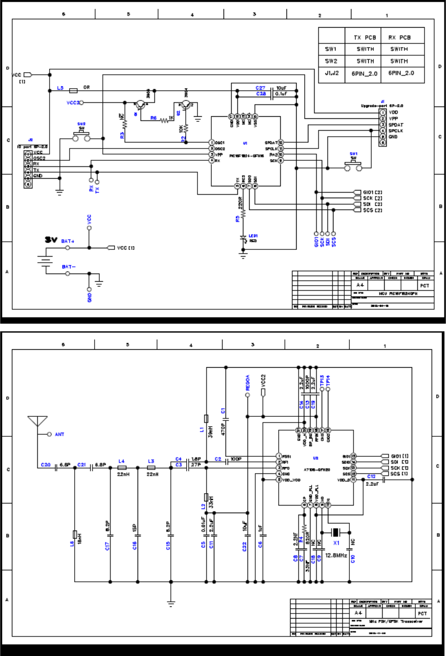
Application Circuit:
V1.4
Professional Computer Technology Limited
Confidential
6
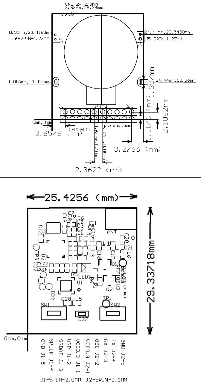
Module Dimension Drawing

V1.4
Professional Computer Technology Limited
Confidential
7
Module Specification
433MHz Transceiver IC Amiccom A7108
Data Rate 150k bps
Modulation FSK
Typical range 10~200M
Output TX Power Max 1.67dBm
Frequency Hooping NO
Operation Power 433MHz:30mA@10dBm, 70mA @ 17dBm
Standby Power < 10uA
NT1R N = 64
Encryption Microchip KEELOQ /CRC
GPIO 1
Switch 2
LED 1
Communication Port UART
FCC Warming:
This equipment has been tested and found to comply with the limits for a
Class B digital device, pursuant to Part 15 of the FCC Rules. These limits are designed to provide
reasonable protection against
harmful interference in a residential installation. This equipment generates, uses and can radiate radio
frequency energy and, if
not installed and used in accordance with the instructions, may cause harmful interference to radio
communications. However,
there is no guarantee that interference will not occur in a particular installation. If this equipment does
cause harmful
interference to radio or television reception,
which can be determined by turning the equipment off and on, the user is encouraged to try to correct the
interference by one or
more of the following measures:
-- Reorient or relocate the receiving antenna.
-- Increase the separation between the equipment and receiver.
-- Connect the equipment into an outlet on a circuit different from that to which the receiver is connected.
-- Consult the dealer or an experienced radio/TV technician for help.
Changes or modifications are not expressly
approved by the manufacturer could void the user's authority to operate the equipment
The following sentence has to be displayed on the outside of device in which the transmitter module is
installed "Contains FCC ID: TFJFSK7108"