Universal Scientific BM-GP-CS-03 Bluetooth Module User Manual Spec BM GP CS 03 03 17 2004
Universal Scientific Industrial Co., Ltd. Bluetooth Module Spec BM GP CS 03 03 17 2004
Manual

All rights are reserved by USI. No part of this technical document can be reproduced in any form without permission of
USI.
1
Federal Communication Commission Interference Statement
This equipment has been tested and found to comply with the limits for a Class B digital
device, pursuant to Part 15 of the FCC Rules. These limits are designed to provide
reasonable protection against harmful interference in a residential installation. This
equipment generates, uses and can radiate radio frequency energy and, if not installed
and used in accordance with the instructions, may cause harmful interference to radio
communications. However, there is no guarantee that interference will not occur in a
particular installation. If this equipment does cause harmful interference to radio or
television reception, which can be determined by turning the equipment off and on, the
user is encouraged to try to correct the interference by one of the following measures:
- Reorient or relocate the receiving antenna.
- Increase the separation between the equipment and receiver.
- Connect the equipment into an outlet on a circuit different from that
to which the receiver is connected.
- Consult the dealer or an experienced radio/TV technician for help.
This device complies with Part 15 of the FCC Rules. Operation is subject to the following
two conditions: (1) This device may not cause harmful interference, and (2) this device
must accept any interference received, including interference that may cause undesired
operation.
FCC Caution: Any changes or modifications not expressly approved by the party
responsible for compliance could void the user's authority to operate this equipment.
IMPORTANT NOTE:
FCC Radiation Exposure Statement:
This equipment complies with FCC radiation exposure limits set forth for an uncontrolled
environment.
This transmitter must not be co-located or operating in conjunction with any other antenna
or transmitter.
Class 2
B
luetooth Module
BM
-
GP
-
CS
-
0
3
Data Sheet
Mar
. 2004 Rev 1.
2

Class 2 Bluetooth Module (BM-GP-CS-03)
All rights are reserved by USI. No part of this technical document can be reproduced in any form without permission of
USI.
2
This device is intended only for OEM integrators under the following conditions:
The transmitter module may not be co-located with any other transmitter or antenna.
As long as conduction above is met, further transmitter test will not be required. However,
the OEM integrator is still responsible for testing their end-product for any additional
compliance requirements required with this module installed (for example, digital device
emissions, PC peripheral requirements, etc.).
IMPORTANT NOTE: In the event that these conditions can not be met (for example
certain laptop configurations or co-location with another transmitter), then the FCC
authorization is no longer considered valid and the FCC ID can not be used on the final
product. In these circumstances, the OEM integrator will be responsible for re-evaluating
the end product (including the transmitter) and obtaining a separate FCC authorization.
End Product Labeling
The final end product must be labeled in a visible area with the following: “Contains TX
FCC ID: IXMBM-GP-CS-03”.
Manual Information That Must be Included
The OEM integrator has to be aware not to provide information to the end user regarding
how to install or remove this RF module in the user’s manual of the end product which
integrate this module.
The users manual for OEM integrators must include the following information in a
prominent location “ IMPORTANT NOTE: To comply with FCC RF exposure compliance
requirements. The antenna must not be co-located or operating in conjunction with any
other antenna or transmitter.

Class 2 Bluetooth Module (BM-GP-CS-03)
All rights are reserved by USI. No part of this technical document can be reproduced in any form without permission of
USI.
3
General Applications
and more can be designed using this ready-to-use module as a surface mount component to enable a rapid
design cycle and short time-to-market.
The SPI (Serial Peripheral Interface) is used only for programming and testing the module. The PCM ports
are used to connect to an external CODEC to provide two-way audio communication or to a PCM audio
stream to and from the host. The HCI can be a standard four wire UART or a USB interface.
Device Terminal Functions
PIO
The Parallel Input Output (PIO) Port is a general-purpose input/output interface to/from BM-GP-CS-03. The
port consists of eight programmable, bi-directional I/O lines, PIO[0:7]. Programmable Input/Output can be
accessed either via an embedded application running on BM-GP-CS-03 or via private channel or
manufacturer-specific HCI commands.
PIO[0] / RXEN
This is a multifunction terminal. Its function is selected by setting the Persistent Store Key
PSKEY_TX/RX_PIO_CONTROL (0x209). It can be used as a programmable I/O, however it will normally be
used to control the radio front-end receive switch.
PIO[1] / TX
This is a multifunction terminal. Its function is selected by setting the Persistent Store Key
PSKEY_TX/RX_PIO_CONTROL (0x209). It can be used as a programmable I/O, however it will normally be
• Laptop and Desktop PCs
• Mobile Phones
• Cordless Headsets
• Personal Digital Assistants (PDAs)
• Computer Accessories (USB Dongles)
• Mice, Keyboards and Joysticks
• Digital Cameras and Camcorders
• Domestic and Industrial Appliances
• FAX
• Printers
• Scanners

Class 2 Bluetooth Module (BM-GP-CS-03)
All rights are reserved by USI. No part of this technical document can be reproduced in any form without permission of
USI.
4
used to control the radio front end transmit switch. Refer to CSR documentation for BlueCore2-External
software.
PIO[2] / USB_PULL_UP
This is a multifunction terminal. On UART versions of BM-GP-CS-03 this terminal is a programmable I/O. On
USB versions, its function is selected by setting the Persistent Store Key PSKEY_USB_PIO_WAKEUP
(0x2cf) either as a programmable I/O or as a USB_WAKE_UP function.
PIO[3] / USB_WAKE_UP
This is a multifunction terminal. On UART versions of BM-GP-CS-03 this terminal is a programmable I/O. On
USB versions, its function is selected by setting the Persistent Store Key PSKEY_USB_PIO_WAKEUP
(0x2cf) either as a programmable I/O or as a USB_WAKE_UP function.
PIO[4] / USB_ON
This is a multifunction terminal. The function depends on whether BM-GP-CS-03 is being used with a USB or
UART connection. On UART versions, this terminal is a programmable Input/Output. For USB versions the
USB_ON function is also selectable.
PO[5] / USB_DETACH
This is a multifunction terminal. The function depends on whether BM-GP-CS-03 is being used with a USB or
UART connection.
On UART versions, this terminal is a programmable Input/Output. For USB versions the USB_DETACH
function is also selectable.
PIO[6]
This is multifunction terminal, its function is determined by Persistent Store Keys. Using
PSKEY_CLOCK_REQUEST_ENABLE, (0x246) this terminal can be configured to be low when
BM-GP-CS-03 is in deep sleep and high when a clock is required. The clock must be supplied within 4ms of
the rising edge of PIO[6] to avoid losing timing accuracy in certain Bluetooth operating modes.
PIO[7] ~ PIO[11]
Programmable Input/Output terminal.
USB Interface
BM-GP-CS-03 contains its own full-speed (12Mbits/s) USB interface. The silicon is compliant with USB
Specification 1.1, available from www.usb.org. Designers of circuits using the USB interface of
Class 2 Bluetooth Module (BM-GP-CS-03)
All rights are reserved by USI. No part of this technical document can be reproduced in any form without permission of
USI.
5
BM-GP-CS-03 are encouraged to read this specification, as it contains valuable information on aspects such
as PCB track impedance, supply inrush current and product labeling.
BM-GP-CS-03 operates as a peripheral USB device, responding to requests from a master host controller
such as a PC. Both the Open Host Control Interface (OHCI) and the Universal Host Control Interface (UHCI)
are supported (see Section H2 of the Bluetooth specification for more information). The set of USB endpoints
implemented behave as specified in the USB section of the Bluetooth specification v1.1, part H2.
As USB is a master-slave-orientated system, BM-GP-CS-03 only supports USB slave operation.
Power Supply
The minimum output high voltage for USB data lines is 2.8V. To safely meet the USB specification, the
voltage on terminals must be an absolute minimum of 3.1V. USI recommends 3.3V for optimal USB signal
quality.
Self-Powered Mode
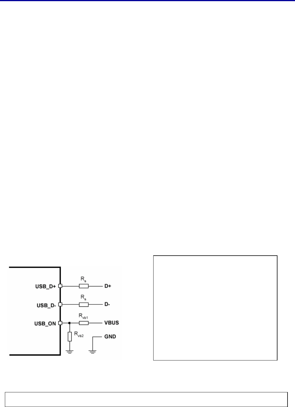
In self-powered mode, the circuit is powered from its own power supply and not from the VBUS (5V) line of
the USB cable. It draws only a small leakage current (below 0.5mA) from VBUS on the USB cable. This is
the easier mode for which to design for, as the design is not limited by the power that can be drawn from the
USB hub or root port. However, it requires that VBUS be connected to BM-GP-CS-03 via a resistor network
(Rvb1 and Rvb2), so module can detect when VBUS is powered up. BM-GP-CS-03 will not pull USB_D+ high
when VBUS is off.
The terminal marked USB_ON can be any free PIO pin. The default is PIO[4]. The PIO pin selected must be
registered by setting PSKEY_USB_PIO_VBUS (0x2d1) to the corresponding pin number.
Figure 4. Self-Powered Mode
Bus-Powered Mode
Rs=24 Ohm, series damping resistor.
Already included in module.
Rvb1 = 47K Ohm, 5%. VBUS ON
sense divider.
Rvb2 = 22K Ohm, 5%. VBUS ON
sense divider.
Rvb1 and Rvb2 must added by user
under self-powered mode.
Class 2 Bluetooth Module (BM-GP-CS-03)
All rights are reserved by USI. No part of this technical document can be reproduced in any form without permission of
USI.
6
In bus-powered mode the application circuit draws its current from the 5V VBUS supply on the USB cable.
BM-GP-CS-03 negotiates with the PC during the USB enumeration stage about power consumption. The 5V
VBUS line emerging from a PC is often electrically noisy. As well as regulation down to 3.3V and 1.8V,
applications should include careful filtering of the 5V line to attenuate noise that is above the voltage
regulator’s bandwidth. Excessive noise on the 1.8V supply to the analogue supply pins of BM-GP-CS-03 will
result in reduced receive sensitivity and a distorted transmit signal.
Detach and Wake_Up Signaling
BM-GP-CS-03 can provide out-of-band signaling to a host controller by using the dedicated control lines
called ‘USB_DETACH’ and ‘USB_WAKE_UP’. These are outside the USB specification (no wires exist for
them inside the USB cable), but can be useful when embedding BM-GP-CS-03 into a circuit where no
external USB is visible to the user. Both control lines are shared with PIO pins and can be assigned to any
PIO pin by setting the Persistent Store Keys PSKEY_USB_PIO_DETACH (0x2ce) and
PSKEY_USB_PIO_WAKEUP (0x2cf) to the selected PIO number).
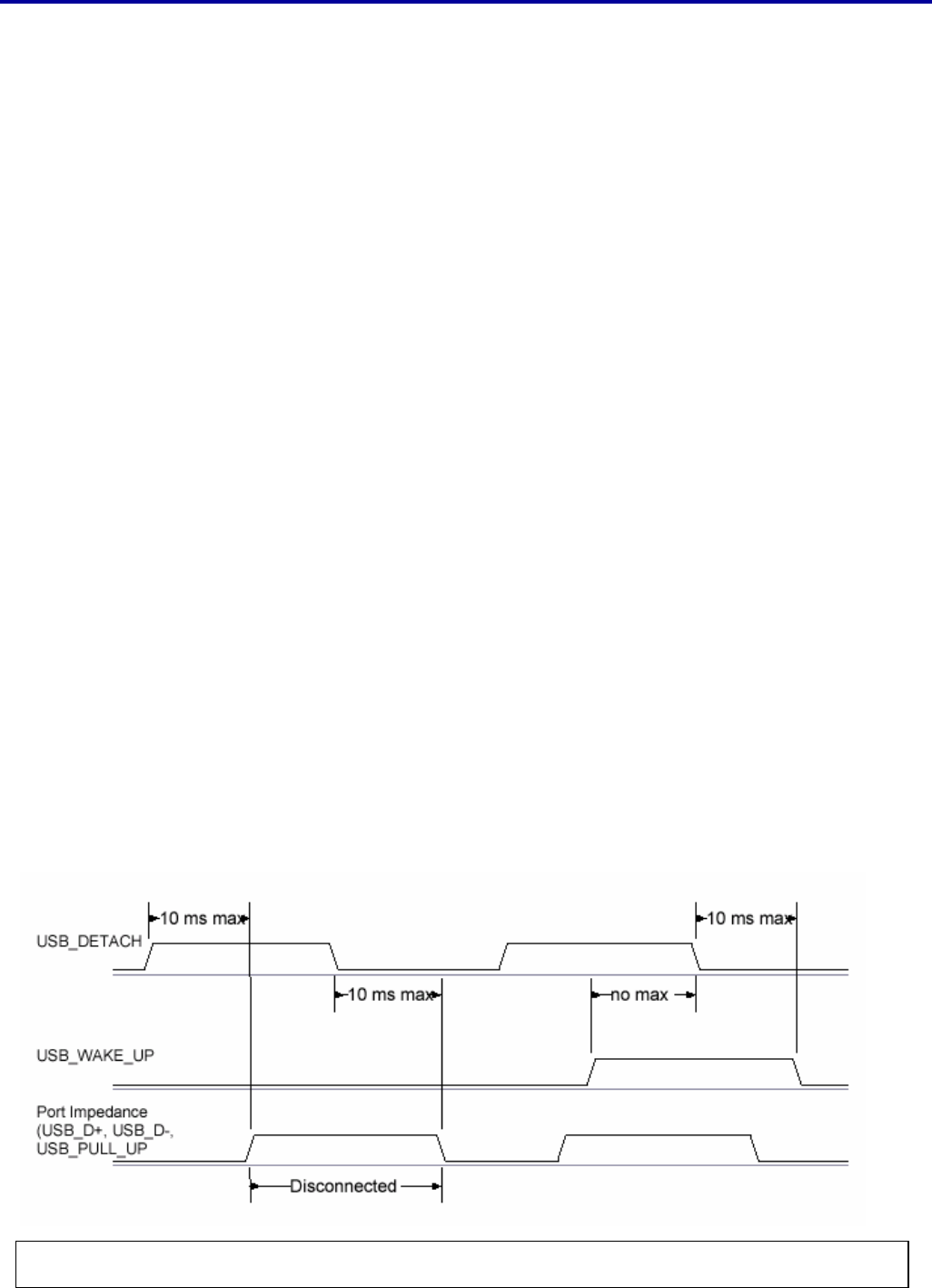
USB_DETACH, is an input which, when asserted high, causes BM-GP-CS-03 to put USB_D- and USB_D+
in a high-impedance state and to 1.5K Ohm?pull-up resistor on USB_D+. This detaches the device from the
bus and is logically equivalent to unplugging the device. When USB_DETACH is taken low, BM-GP-CS-03
will connect
back to USB and await enumeration by the USB host.
USB_WAKE_UP, is an active high output (used only when USB_DETACH is active) to wake up the host and
allow USB communication to recommence. It replaces the function of the software USB WAKE_UP message
(which runs over the USB cable proper), and cannot be sent while BM-GP-CS-03 is effectively disconnected
from the bus.
Figure 5. USB_DETACH and USB_WAKE_UP Signal

Class 2 Bluetooth Module (BM-GP-CS-03)
All rights are reserved by USI. No part of this technical document can be reproduced in any form without permission of
USI.
7
USB Driver
A USB Bluetooth device driver is required to provide a software interface between BM-GP-CS-03 and
Bluetooth applications running on the host.
USB 1.1 Compliance
BM-GP-CS-03 is compatible with the USB specification v1.1, details of which are available from
http://www.usb.org. The specification contains valuable information on aspects such as PCB track
impedance, supply inrush current and product labeling. Although BM-GP-CS-03 meets the USB specification,
USI cannot guarantee that an application circuit designed around the chip is USB compliant. The choice of
application circuit, component choice and PCB layout all affect USB signal quality and electrical
characteristics. Independent USB qualification must be sought before an application is deemed USB
compliant and can bear the USB logo. Such qualification can be obtained from a USB plug fest or from an
independent USB test house.
Terminals USB_D+ and USB_D- adhere to the USB specification 1.1 electrical requirements. For AC and DC
specifications for terminals USB_DETACH, USB_WAKE_UP, USB_PULL_UP and USB_ON, refer to PIO
specification.
USB 2.0 Compatibility
BM-GP-CS-03 is compatible with USB specification 2.0 masters; under these circumstances the two ends
agree the mutually acceptable rate of 12Mbits/s according to the USB 2.0 specification.
PCM
Pulse Code Modulation (PCM) is the standard method used to digitize human voice patterns for transmission
over digital communication channels. Through its PCM interface, BM-GP-CS-03 has hardware support for
continual transmission and reception of PCM data, thus reducing processor overhead for wireless headset
applications. BM-GP-CS-03 offers a bi-directional digital audio interface that routes directly into the
baseband layer of the on-chip firmware. It does not pass through the HCI protocol layer.
Hardware on BM-GP-CS-03 allows the data to be sent to and received from a SCO connection.
Up to three SCO connections can be supported by the PCM interface at any one time.
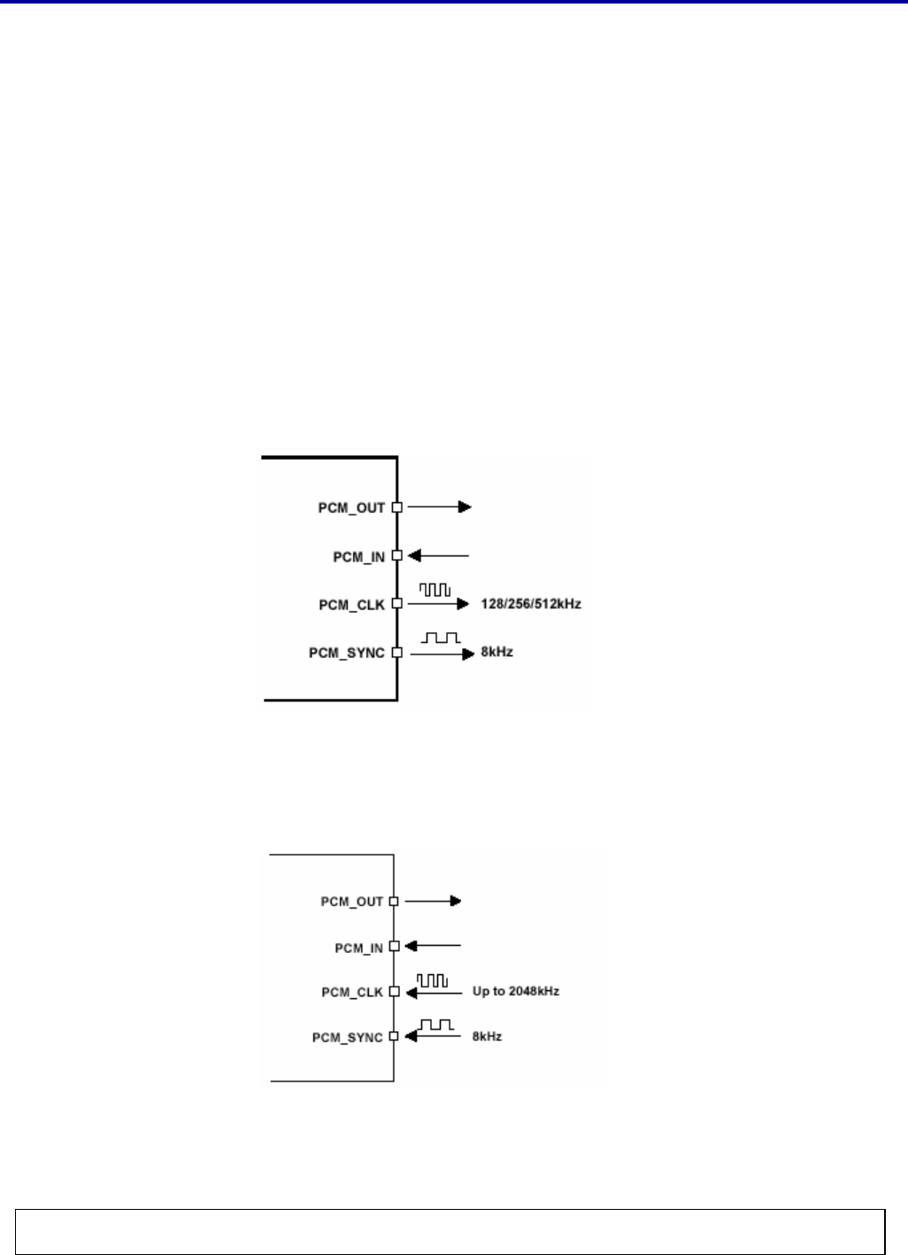
BM-GP-CS-03 can operate as the PCM interface Master generating an output clock of 128, 256 or 512kHz.
When configured as PCM interface slave it can operate with an input clock up to 2048kHz. BM-GP-CS-03 is
compatible with a variety of clock formats, including Long Frame Sync, Short Frame Sync and GCI timing
environments. It supports 13 or 16-bit linear, 8-bit u-law or A-law companded sample formats at 8ksamples/s
Class 2 Bluetooth Module (BM-GP-CS-03)
All rights are reserved by USI. No part of this technical document can be reproduced in any form without permission of
USI.
8
and can receive and transmit on any selection of three of the first four slots following PCM_SYNC. The PCM
configuration options are enabled by setting the Persistent Store Key PS KEY_PCM_CONFIG (0x1b3).
BM-GP-CS-03 interfaces directly to PCM audio devices includes the following:
l Qualcomm MSM 3000 series and MSM 5000 series CDMA baseband devices
l OKI MSM7705 four channel A-law and u-law CODEC
l Motorola MC145481 8-bit A-law and u-law CODEC
l Motorola MC145483 13-bit linear CODEC
l BM-GP-CS-03 is also compatible with the Motorola SSI TM interface
PCM Interface Master/Slave
When configured as the Master of the PCM interface, BM-GP-CS-03 generates PCM_CLK and PCM_SYNC.
Figure 6. BM-GP-CS-03 configured as PCM interface master
When configured as the Slave of the PCM interface, BM-GP-CS-03 accepts PCM_CLK rates up to 2048kHz.
Figure 7. BM-GP-CS-03 configured as PCM interface slave
Class 2 Bluetooth Module (BM-GP-CS-03)
All rights are reserved by USI. No part of this technical document can be reproduced in any form without permission of
USI.
9
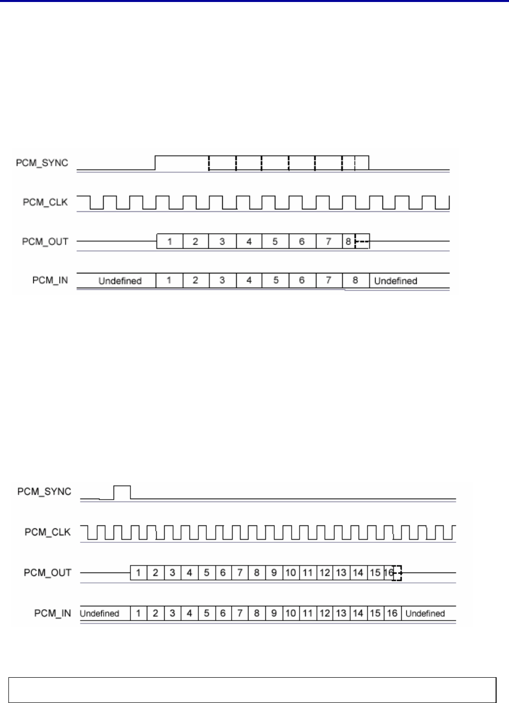
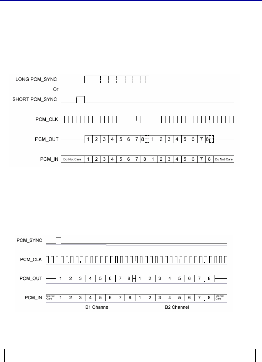
Long Frame Sync
Long Frame Sync is the name given to a clocking format that controls the transfer of PCM data words or
samples. In Long Frame Sync, the rising edge of PCM_SYNC indicates the start of the PCM word. When
BM-GP-CS-03 is configured as PCM Master, generating PCM_SYNC and PCM_CLK, then PCM_SYNC is
8-bits long. When BM-GP-CS-03 is configured as PCM Slave, PCM_SYNC may be from two consecutive
falling edges of PCM_CLK to half the PCM_SYNC rate (i.e., 62.5s) long.
Figure 8. Long Frame Sync (Shown with 8-bit Companded Sample)
BM-GP-CS-03 samples PCM_IN on the falling edge of PCM_CLK and transmits PCM_OUT on the rising
edge. PCM_OUT may be configured to be high impedance on the falling edge of PCM_CLK in the LSB
position or on the rising edge.
Short Frame Sync
In Short Frame Sync the falling edge of PCM_SYNC indicates the start of the PCM word. PCM_SYNC is
always one clock cycle long.
Figure 9. Short Frame Sync (Shown with 16-bit Sample)
As with Long Frame Sync, BM-GP-CS-03 samples PCM_IN on the falling edge of PCM_CLK and transmits
Class 2 Bluetooth Module (BM-GP-CS-03)
All rights are reserved by USI. No part of this technical document can be reproduced in any form without permission of
USI.
10
PCM_OUT on the rising edge. PCM_OUT may be configured to be high impedance on the falling edge of
PCM_CLK in the LSB position or on the rising edge.
Multi-Slot Operation
More than one SCO connection over the PCM interface is supported using multiple slots. Up to three SCO
connections can be carried over any of the first four slots.
Figure 10. Multi-slot Operation with Two Slots and 8-bit Companded Samples
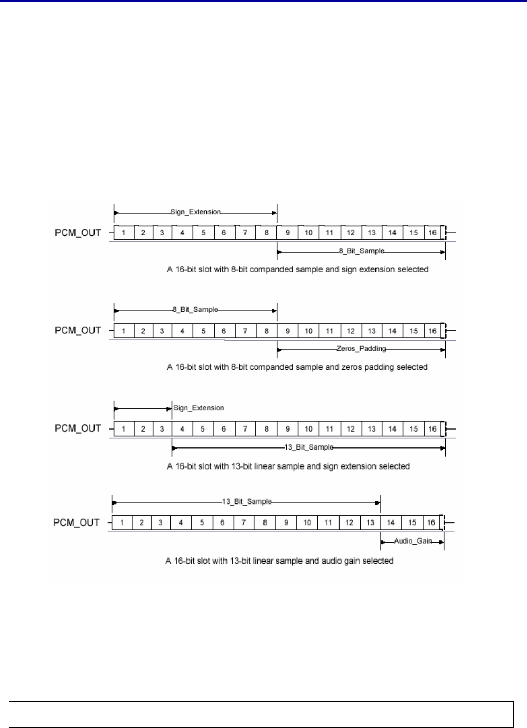
GCI Interface
BM-GP-CS-03 is compatible with the General Circuit Interface, a standard synchronous 2B+D ISDN timing
interface. The two 64Kbps B channels can be accessed when this mode is configured.
Figure 11. GCI Interface
The start of frame is indicated by the rising edge of PCM_SYNC and runs at 8kHz. With BM-GP-CS-03 in
Class 2 Bluetooth Module (BM-GP-CS-03)
All rights are reserved by USI. No part of this technical document can be reproduced in any form without permission of
USI.
11
Slave mode, the frequency of PCM_CLK can be up to 4.096MHz.
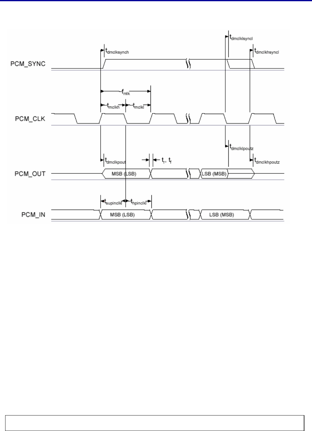
Slots and Sample Formats
BM-GP-CS-03 can receive and transmit on any selection of the first four slots following each sync pulse. Slot
durations can be either 8 or 16 clock cycles. Durations of 8 clock cycles may only be used with 8-bit sample
formats. Durations of 16 clocks may be used with 8, 13 or 16-bit sample formats. BM-GP-CS-03 supports
13-bit linear, 16-bit linear and 8-bit u-law or A-law sample formats. The sample rate is 8ksamples/s. The bit
order may be little or big endian. When 16-bit slots are used, the 3 or 8 unused bits in each slot may be filled
with sign extension, padded with zeros or a programmable 3-bit audio attenuation compatible with some
Motorola CODECs.
Figure 12. 16-bit Slot Length and Sample Formats
Additional Features
BM-GP-CS-03 has a mute facility that forces PCM_OUT to be 0. In Master mode, PCM_SYNC may also be
forced to 0 while keeping PCM_CLK running (which some CODECS use to control power-down).
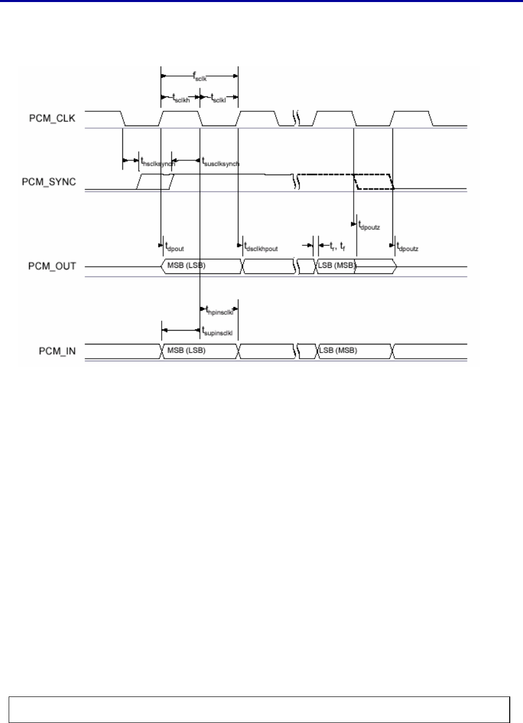
PCM Timing Information - PCM Master Timing

Class 2 Bluetooth Module (BM-GP-CS-03)
All rights are reserved by USI. No part of this technical document can be reproduced in any form without permission of
USI.
12
Symbol Parameter Min Typ Max Unit
128
fmclk PCM_CLK frequency - 256 - kHz
512
- PCM_SYNC frequency - 8 kHz
fmclkh (1) PCM_CLK high 980 - - ns
tmclkl (1) PCM_CLK low 730 - - ns
tdmclksynch Delay time from PCM_CLK high to
PCM_SYNC high - - 20 ns
tdmclkpout Delay time from PCM_CLK high to valid
PCM_OUT - - 20 ns
tdmclklsyncl Delay time from PCM_CLK low to
PCM_SYNC low (Long Frame Sync only) - - 20 ns
tdmclkhsyncl Delay time from PCM_CLK high to
PCM_SYNC low - - 20 ns
tdmclklpoutz Delay time from PCM_CLK low to
PCM_OUT high impedance - - 20 ns
tdmclkhpoutz Delay time from PCM_CLK high to
PCM_OUT high impedance - - 20 ns
tsupinclkl Set-
up time for PCM_IN valid to PCM_CLK
low 30 - - ns
thpinclkl Hold time for PCM_CLK low to PCM_IN
invalid 30 - - ns
tr Edge rise time (Cl = 50 pf, 10-90 %) - - 15 ns
tf Edge fall time (Cl = 50 pf, 10-90 %) - - 15 ns
Note: Assumes normal system clock operation. Figures will vary during low power modes, when system
clock speeds are reduced.
Class 2 Bluetooth Module (BM-GP-CS-03)
All rights are reserved by USI. No part of this technical document can be reproduced in any form without permission of
USI.
13
Figure 13. PCM Master Timing

Class 2 Bluetooth Module (BM-GP-CS-03)
All rights are reserved by USI. No part of this technical document can be reproduced in any form without permission of
USI.
14
PCM Timing Information - PCM Slave Timing
Symbol Parameter Min Typ Max Unit
fsclk PCM clock frequency (Slave mode: input) 64 - - kHz
fsclk PCM clock frequency (GCI mode) 128 - - kHz
tsclkl PCM_CLK low time 200 - - ns
tsclkh PCM_CLK high time 200 - - ns
thsclksynch Hold time from PCM_CLK low to
PCM_SYNC high 30 - - ns
tsusclksynch Set-up time for PCM_SYNC high to
PCM_CLK low 30 - - ns
tdpout Delay time from PCM_SYNC or PCM_CLK
whichever is later, to valid PCM_OUT data
(Long Frame Sync only)
- - 20 ns
tdsclkhpout Delay time from CLK high to PCM_OUT
valid data - - 20 ns
tdpoutz Delay time from PCM_SYNC or PCM_CLK
low, whichever is later, to PCM_OUT data
line high impedance
- - 20 ns
tsupinsclkl Set-up time for PCM_IN valid to CLK low 30 - - ns
thpinsclkl Hold time for PCM_CLK low to PCM_IN
invalid 30 - - ns
tr Edge rise time (Cl = 50 pF, 10-90 %) - - 15 ns
tf Edge fall time (Cl = 50 pF, 10-90 %) - - 15 ns
Class 2 Bluetooth Module (BM-GP-CS-03)
All rights are reserved by USI. No part of this technical document can be reproduced in any form without permission of
USI.
15
Figure 15. PCM Slave Timing
Class 2 Bluetooth Module (BM-GP-CS-03)
All rights are reserved by USI. No part of this technical document can be reproduced in any form without permission of
USI.
16
UART Interface
BM-GP-CS-03 Universal Asynchronous Receiver Transmitter (UART) interface provides a simple mechanism
for communicating with other serial devices using the RS232 standard(1).
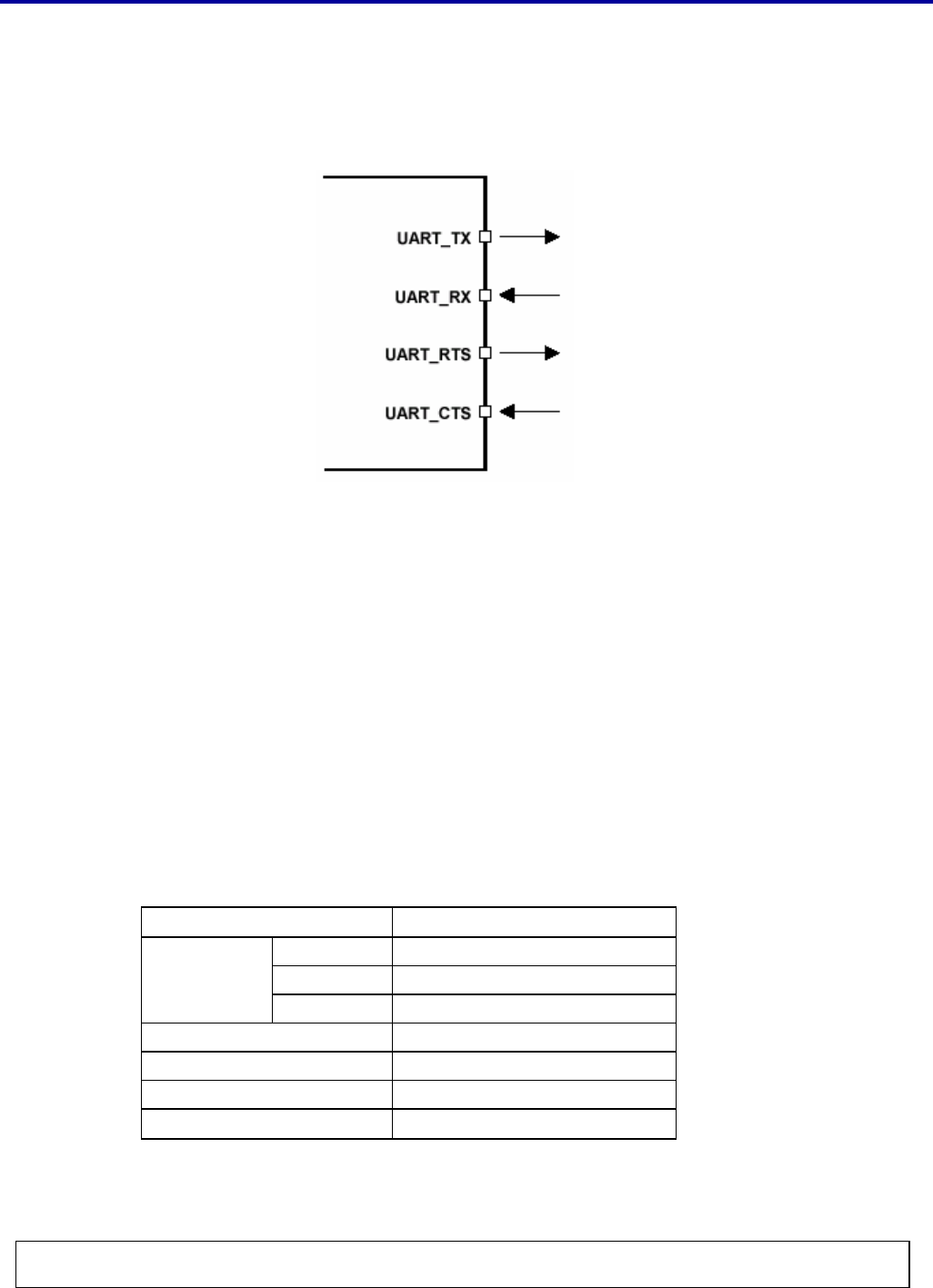
Figure 16. Universal Asynchronous Receiver
Four signals are used to implement the UART function, as shown in above figure. When BM-GP-CS-03 is
connected to another digital device, UART_RX and UART_TX transfer data between the two devices. The
remaining two signals, UART_CTS and UART_RTS, can be used to implement RS232 hardware flow control
where both are active low indicators. All UART connections are implemented using CMOS technology and
have signaling levels of 0V and VDD_PADS.
UART configuration parameters, such as Baud rate and packet format, are set using PSTool software.
Notes:
In order to communicate with the UART at its maximum data rate using a standard PC, an accelerated serial
port adapter card is required for the PC.
Uses RS232 protocol but voltage levels are 0V to VDD_PADS, (requires external RS232 transceiver IC)
Parameter
Possible Values
Minimum 1200 Baud (<2% Error)
Baud Rate Default 115.2KBaud (<1% Error)
Maximum 1.5MBaud (<1% Error)
Flow Control
RTS/CTS or None
Parity
None, Odd or Even
Number of Stop Bits 1 or 2
Bits per channel 8
Please specify your needs when ordering the modules with UART interface.
Class 2 Bluetooth Module (BM-GP-CS-03)
All rights are reserved by USI. No part of this technical document can be reproduced in any form without permission of
USI.
17
Mounting Guide for Antenna Radiation
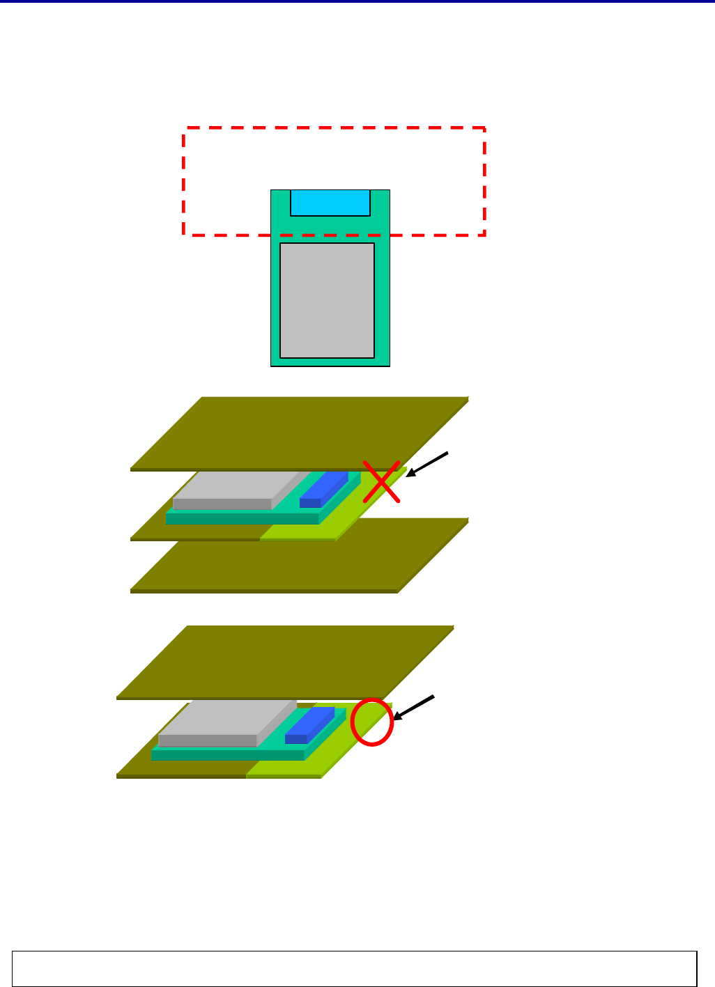
In order to achieve longest communication range, please keep the area surrounding antenna free of
grounding or metal housing.
BM -GP-CS-03
Antenna
Ground should not come in this area
Ground
Do not completely
cover the antenna
portion with ground
plates
.
Ground
Ground Ground
Ground
Covering only one side
of the antenna is
acceptable.
But the distance
between ground plate
and antenna should be
keep as far as
Ground
All rights are reserved by USI. No part of this technical document can be reproduced in any form without permission of
USI.
1
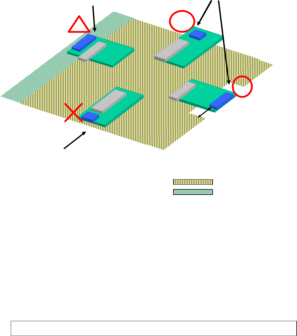
Mounting Position in Various Applications
PCB with Ground Plane
PCB without Ground Plane
If mounted at an inner portion of the PCB grounded,
no sufficient antenna performance will be available.
> 5mm
(Recommend)
If there is PCB or other material under the
antenna area, antenna will be de-tuned
from its resonant frequency. Impedance
re-matching is needed.
When mounting BM-GP-CS-03on a PCB,
locate it at (or near) the edge of the PCB

Class 2 Bluetooth Module (BM-GP-CS-03)
All rights are reserved by USI. No part of this technical document can be reproduced in any form without permission of
USI.
19
Impedance Matching of Antenna
BM-GP-CS-03 utilizes a mono-pole ceramic chip antenna for radio communication. Application environments,
such as notebooks, PDAs, headsets or other handheld devices, both have plastic housings, different
motherboards and other mechanism structures. These factors will cause the deviation of antenna resonant
frequency, but can be corrected by antenna matching. In order to achieve longest communication range, it is
recommended to optimize the antenna matching in the final product. Please consult USI for further information.
Class 2 Bluetooth Module (BM-GP-CS-03)
All rights are reserved by USI. No part of this technical document can be reproduced in any form without permission of
USI.
20
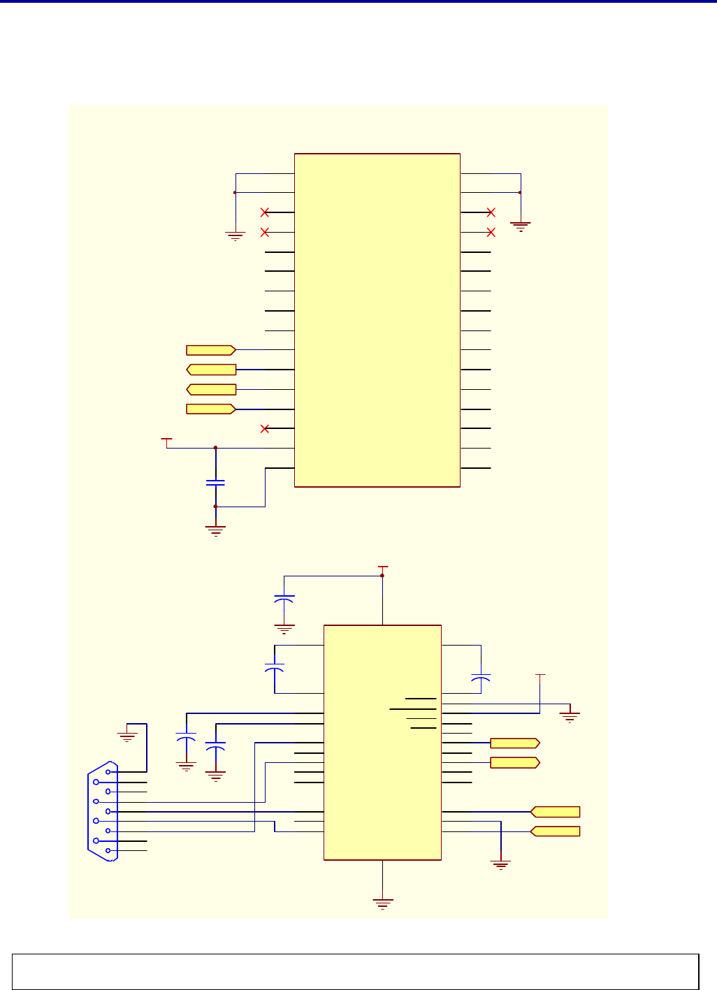
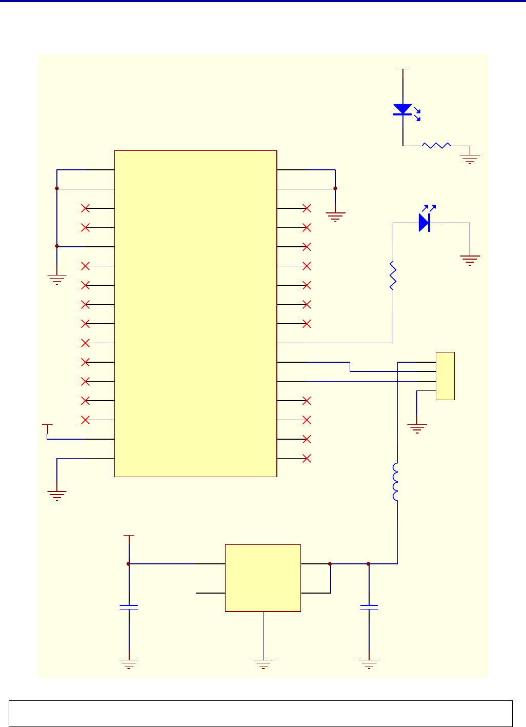
Application Circuits
Application Circuit of UART Interface
3V3
UART_TX
UART_RX
UART_RTS
UART_CTS
C1
2.2uF
C2+
1
C2-
2
V-
3
R1IN
4
R2IN
5
R3IN
6
R4IN
7
R5IN
8
T1OUT
9
T2OUT
10
T3OUT
11 T3IN 12
T2IN 13
T1IN 14
R5OUT 15
R4OUT 16
R3OUT 17
R2OUT 18
R1OUT 19
R2OUT 20
STATUS 21
SHUTDOWN 22
ONLINE 23
C1- 24
GND
25 Vcc 26
V+
27
C1+ 28
U2
MAX3245ECWI
+C3
0.1uF +C4
0.1uF
+
C6
0.1uF +C2
0.1uF
+C5
0.1uF
1
6
2
7
3
8
4
9
5
J1
DB9
UART_TX
UART_RTS
UART_RX
UART_CTS
3V3
3V3
GND
1
GND
2
AIO(0)
3
AIO(1)
4
RESET
5
SPI_MISO
6
SPI_CSB
7
SPI_CLK
8
SPI_MOSI
9
UART_CTS
10
UART_TX
11
UART_RTS
12
UART_RX
13
1V8
14
3V3
15
GND
16
PCM_SYNC 18
PCM_IN 19
PCM_CLK 20
USB_D+ 21
USB_D- 22
PIO(7)/RAM_CSB 23
PIO(6)/CLK_REQ 24
PIO(5)/USB_DETACH 25
PIO(4)/USB_ON 26
PIO(3)/USB_WAKE_UP 27
PIO(2)/USB_PULL_UP 28
PIO(1)/TXEN 29
PIO(0)/RXEN 30
GND 31
GND 32
PCM_OUT 17
U1
BM-GP-CS-03
Class 2 Bluetooth Module (BM-GP-CS-03)
All rights are reserved by USI. No part of this technical document can be reproduced in any form without permission of
USI.
21
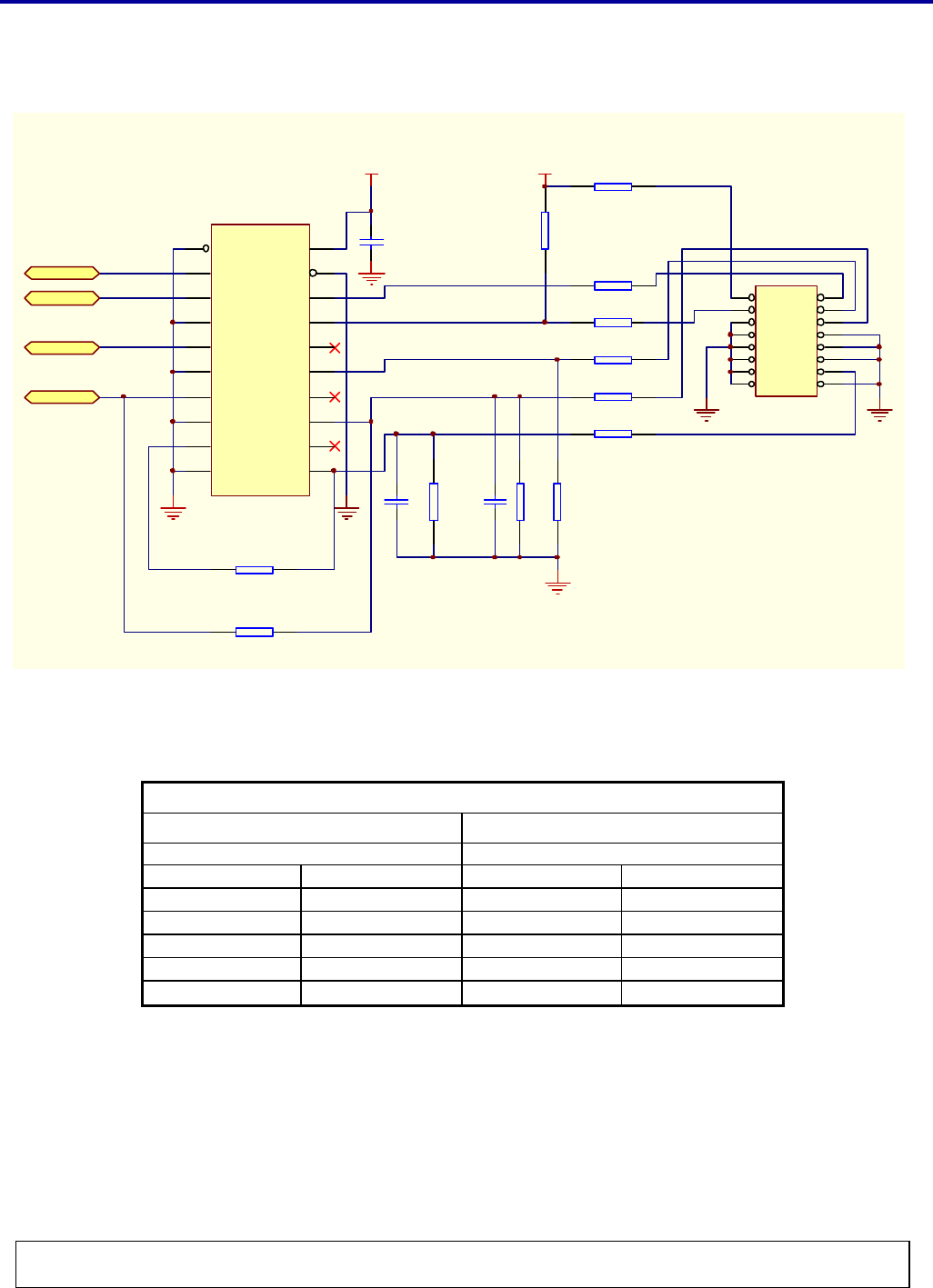
Application Circuit of USB Dongle
1
2
3
4
J1
USB
1:+5VUSB
2:D-
3:D+
4:GND
IN 1
EN 3
GND
2
OUT
5
NC
4
U2
XC6204B332MR
3V3
3V3
Rx
LED
R4
470R
Power
LED
R3
470R
3V3
GND
1
GND
2
AIO(0)
3
AIO(1)
4
RESET
5
SPI_MISO
6
SPI_CSB
7
SPI_CLK
8
SPI_MOSI
9
UART_CTS
10
UART_TX
11
UART_RTS
12
UART_RX
13
1V8
14
3V3
15
GND
16
PCM_SYNC 18
PCM_IN 19
PCM_CLK 20
USB_D+ 21
USB_D- 22
PIO(7)/RAM_CSB 23
PIO(6)/CLK_REQ 24
PIO(5)/USB_DETACH 25
PIO(4)/USB_ON 26
PIO(3)/USB_WAKE_UP 27
PIO(2)/USB_PULL_UP 28
PIO(1)/TXEN 29
PIO(0)/RXEN 30
GND 31
GND 32
PCM_OUT 17
U1
BM-GP-CS-03 L1
10uH
C1
2.2uF
C2
2.2uF
Class 2 Bluetooth Module (BM-GP-CS-03)
All rights are reserved by USI. No part of this technical document can be reproduced in any form without permission of
USI.
22
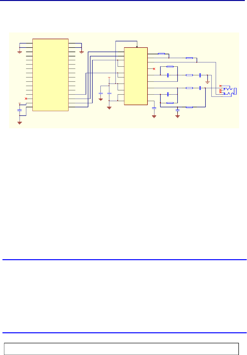
Application Circuit of SPI Interface
CN1 to DB-25 Printer Port connection
SPI/LPT PORT MAPPING
SPI LPT
16W IDC 25W D-TYPE
SPI_MISO PIN 2 ACKNOWLEDGE
PIN 10
SPI_CSB PIN 3 DATA[0] PIN 2
SPI_MOSI PIN 4 DATA[6] PIN 8
SPI_CLK PIN 6 DATA[7] PIN 9
XAP_RESET PIN 14 INIT PIN 16
GROUND PIN 5, 7~13,15,16
GROUND PIN 18~ PIN25
1 2
3 4
5 6
7 8
910
11 12
13 14
15 16
CN2
PIN_HEADER_D16
R13 100R
R7
1K
R8
1K
R9
1K
C1
0.1uF
3V3
R10
1K
R14
100K
R15
100K
R5
10K
R3
10K R4
10K
C13
10pF
C12
10pF
R1
10K
R6
47R
3V3
1OE
1
1A0
2
2Y0
3
1A1
4
2Y1
5
1A2
6
2Y2
7
1A3
8
2Y3
9
GND
10
1Y0 18
2A0 17
1Y1 16
2A1 15
1Y2 14
2A2 13
1Y3 12
2A3 11
2OE 19
VCC 20
U1
74LCX244
SPI_MISO
SPI_CSB
SPI_MOSI
SPI_CLK
Class 2 Bluetooth Module (BM-GP-CS-03)
All rights are reserved by USI. No part of this technical document can be reproduced in any form without permission of
USI.
23
Application Circuit of PCM Interface
For Additional information, please contact the following:
Universal Scientific Industrial Co., Ltd.
Headquarters
141, Lane 351, Taiping Road, Sec. 1 , Tsao-Tuen , Taiwan,
Http://www.usi.com.tw
Tel: + 886-49-2350876, 2325876
Fax: +886-49-3439561, 2337360,2351093
E-mail:usi@ms.usi.com.tw
VSS
15
HB
16
RO- 2
PI 3
PO- 4
PO+ 5
TG 17
TI- 18
TI+ 19
VAG 20
VAG REF 1
DR
8
DT
13
FST
14
FSR
7
MCLK
11
BCLKT
12
BCLKR
9
VDD
6
PDI 10
U2
MC145483SD
C3
0.1uF
C16
10uF
3V3
R2
10K R20
22K
R19
68K
R11
1K
R12
1K
R21
1K5
R18
68K
C18
470pF
C6
0.1uF
C4
0.1uF
C17
470pF
C5
0.1uF
C19
10nF
1
2
3
4
5
6
J1
PHONE JACK
C1
2.2uF
GND
1
GND
2
AIO(0)
3
AIO(1)
4
RESET
5
SPI_MISO
6
SPI_CSB
7
SPI_CLK
8
SPI_MOSI
9
UART_CTS
10
UART_TX
11
UART_RTS
12
UART_RX
13
1V8
14
3V3
15
GND
16
PCM_SYNC 18
PCM_IN 19
PCM_CLK 20
USB_D+ 21
USB_D- 22
PIO(7)/RAM_CSB 23
PIO(6)/CLK_REQ 24
PIO(5)/USB_DETACH 25
PIO(4)/USB_ON 26
PIO(3)/USB_WAKE_UP 27
PIO(2)/USB_PULL_UP 28
PIO(1)/TXEN 29
PIO(0)/RXEN 30
GND 31
GND 32
PCM_OUT 17
U1
BM-GP-CS-03
3V3