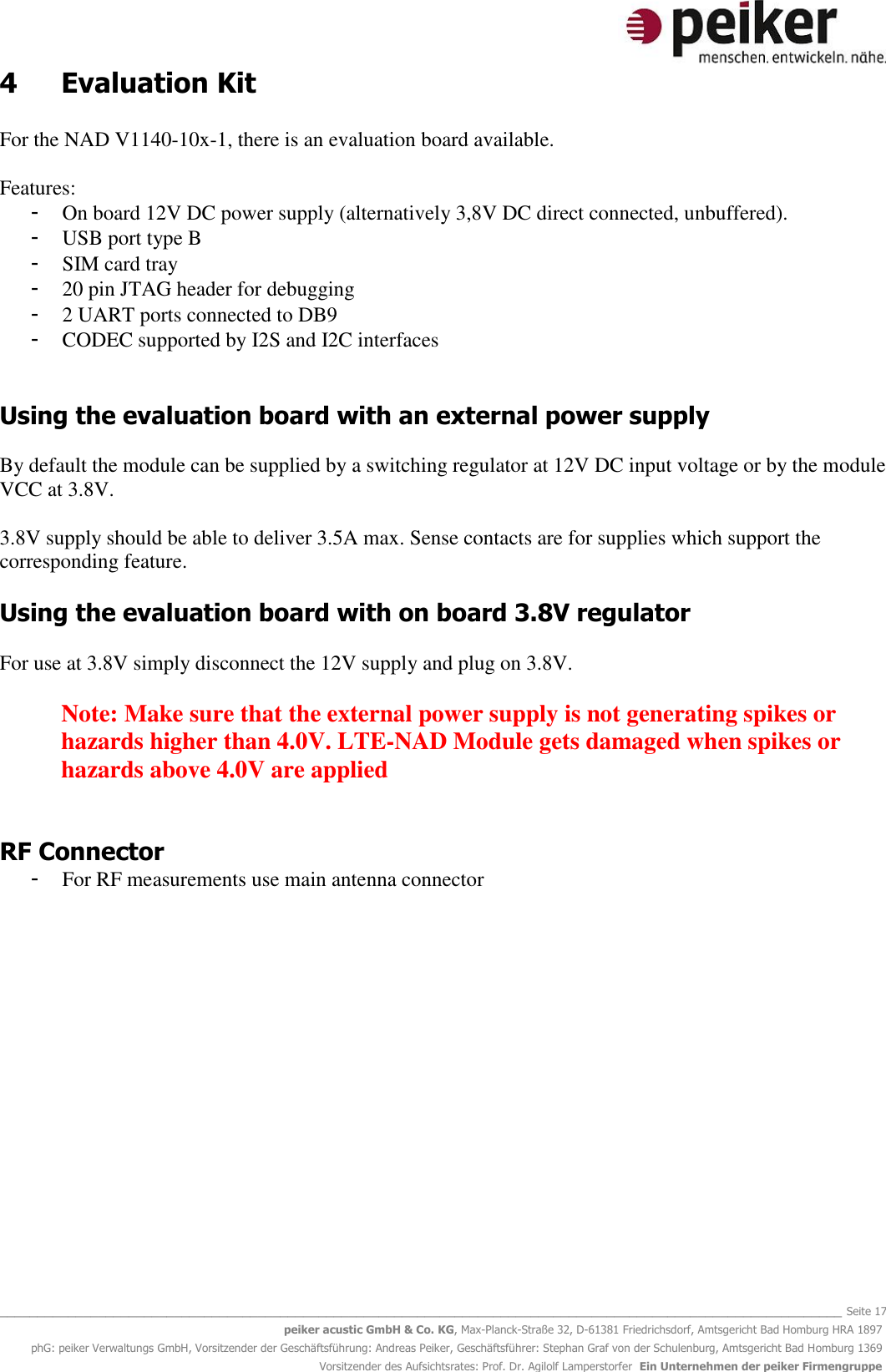
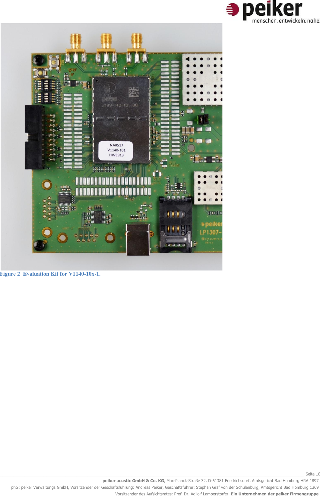
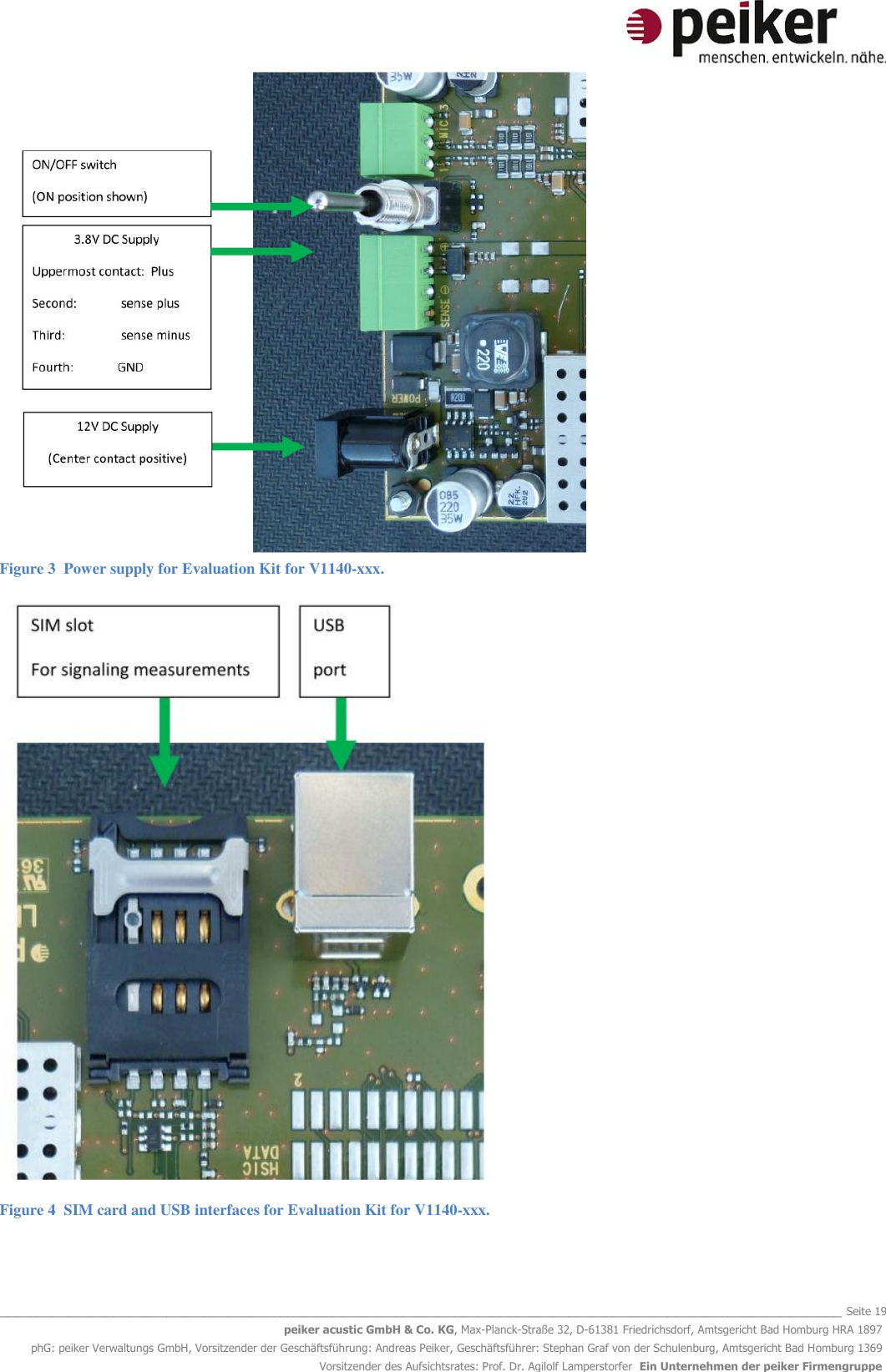
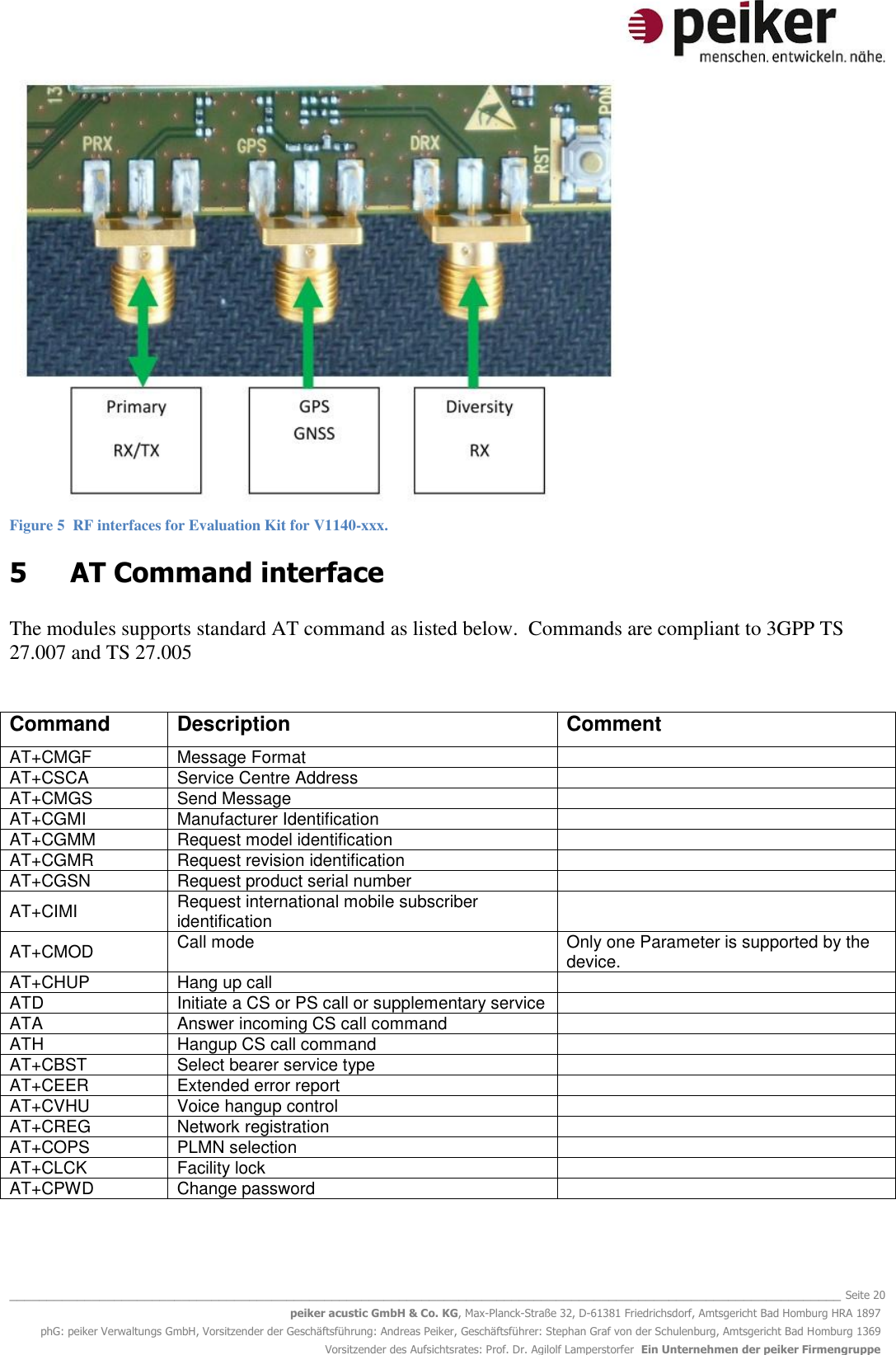
VALEO Telematik und Akustik V1140-104-1 GSM/GRPRS/UMTS/HSDPA/HSUPA/LTE Module User Manual v1140 10x 1 usermanual v16

Peiker acustic GmbH & Co. KG GSM/GRPRS/UMTS/HSDPA/HSUPA/LTE Module v1140 10x 1 usermanual v16

v1140-10x-1_usermanual_v16

  _______________________________________________________________________________________________________________ Seite 1 peiker acustic GmbH & Co. KG, Max-Planck-Straße 32, D-61381 Friedrichsdorf, Amtsgericht Bad Homburg HRA 1897 phG: peiker Verwaltungs GmbH, Vorsitzender der Geschäftsführung: Andreas Peiker, Geschäftsführer: Stephan Graf von der Schulenburg, Amtsgericht Bad Homburg 1369 Vorsitzender des Aufsichtsrates: Prof. Dr. Agilolf Lamperstorfer  Ein Unternehmen der peiker Firmengruppe User manual  LTE-NAD V1140-10x-1            Peiker product IDs:    2189-140-133-00 (V1140-103-1)  2189-140-170-00 (V1140-100-1)          2189-140-174-00 (V1140-104-1)         2189-140-176-00 (V1140-106-1) 2189-140-181-00 (V1140-101-1)               Revision:      1.6 Date:        May 2016  Status:       Release
  _______________________________________________________________________________________________________________ Seite 2 peiker acustic GmbH & Co. KG, Max-Planck-Straße 32, D-61381 Friedrichsdorf, Amtsgericht Bad Homburg HRA 1897 phG: peiker Verwaltungs GmbH, Vorsitzender der Geschäftsführung: Andreas Peiker, Geschäftsführer: Stephan Graf von der Schulenburg, Amtsgericht Bad Homburg 1369 Vorsitzender des Aufsichtsrates: Prof. Dr. Agilolf Lamperstorfer  Ein Unternehmen der peiker Firmengruppe History:  Date Revision Name Comment 30.11.2015 1.0 Phse Initial document based on V1140-xxx documents 12.01.2016 1.1 Phse Added some missing Product IDs on the cover page Corrected the FCC ID and IC ID of V1140-103-1 in section 8.3 20.01.2016 1.2 Phse Removed LTE B8 support for V1140-100-1  22.03.2016 1.3 Phse Updated sections 2.3 and 8.3 30.03.2016 1.4 Phse Updated sections 2.1 to 2.3 with V1140-101-2 Deleted “eCall inband modem” from section 2.2  Updated the List of Acronyms and moved it to the end 04.04.2016 1.5 Phse Deleted V1140-103-1 and V1140-104-1 from section 7.3 IC Labeling 17.05.2016 1.6 Phse Added section 2.2 Reworked section 7.3 OEM Responsibilities / Antenna
  _______________________________________________________________________________________________________________ Seite 3 peiker acustic GmbH & Co. KG, Max-Planck-Straße 32, D-61381 Friedrichsdorf, Amtsgericht Bad Homburg HRA 1897 phG: peiker Verwaltungs GmbH, Vorsitzender der Geschäftsführung: Andreas Peiker, Geschäftsführer: Stephan Graf von der Schulenburg, Amtsgericht Bad Homburg 1369 Vorsitzender des Aufsichtsrates: Prof. Dr. Agilolf Lamperstorfer  Ein Unternehmen der peiker Firmengruppe Content 1 Introduction .......................................................................................................................................... 4 1.1 Scope .................................................................................................................................................. 4 1.2 Audience ............................................................................................................................................ 4 1.3 Contact information, Support ......................................................................................................... 4 2 Overview ............................................................................................................................................... 5 2.1 Product Variants ................................................................................................................................ 5 2.2 Module to Hosts Mapping ................................................................................................................ 6 2.3 Features ............................................................................................................................................. 6 2.4 Approvals ........................................................................................................................................... 7 3 Overview ............................................................................................................................................... 8 3.1 HW Features ...................................................................................................................................... 8 3.2 Connectors ......................................................................................................................................... 8 3.2.1 Module Signal and RF Connectors .......................................................................................... 8 3.2.2 Ground and Heat Dissipation Connectors .............................................................................. 8 3.3 Main Interfaces ................................................................................................................................. 9 3.3.1 USB .............................................................................................................................................. 9 3.3.2 SIM Interface ............................................................................................................................. 9 3.3.3 Power on ..................................................................................................................................... 9 3.3.4 Reset ........................................................................................................................................... 9 3.3.5 GPIOs ........................................................................................................................................ 10 3.3.6 GSBIs ......................................................................................................................................... 10 3.3.7 Module Pin-out ......................................................................................................................... 11 3.4 Supply Voltage ................................................................................................................................ 15 3.5 Power Consumption ....................................................................................................................... 15 3.8 Environmental Specification .......................................................................................................... 16 3.8.1 Temperature Range ................................................................................................................ 16 4 Evaluation Kit ..................................................................................................................................... 17 5 AT Command interface ..................................................................................................................... 20 6 Safety Recommendations according to EN60950-1 ..................................................................... 22 7  Regulatory Certifications .................................................................................................................. 23 7.1 USA (FCC) .................................................................................................................................... 23 7.1.1 FCC Warnings and Notices ................................................................................................. 23 7.2 Canada (IC) ................................................................................................................................. 23 7.3 OEM Responsibilities .................................................................................................................. 24 8 List of Acronyms ................................................................................................................................ 27
  _______________________________________________________________________________________________________________ Seite 4 peiker acustic GmbH & Co. KG, Max-Planck-Straße 32, D-61381 Friedrichsdorf, Amtsgericht Bad Homburg HRA 1897 phG: peiker Verwaltungs GmbH, Vorsitzender der Geschäftsführung: Andreas Peiker, Geschäftsführer: Stephan Graf von der Schulenburg, Amtsgericht Bad Homburg 1369 Vorsitzender des Aufsichtsrates: Prof. Dr. Agilolf Lamperstorfer  Ein Unternehmen der peiker Firmengruppe 1  Introduction  1.1 Scope This document gives an overview about electrical, mechanical and functional detail of the peiker LTE-NAD V1140-10x-1 modules. 1.2 Audience Information to integrate the module in other applications.   1.3 Contact information, Support peiker acustic GmbH & Co KG  Max-Planck Street 32 D-61381 Friedrichsdorf / Ts. Germany  http://www.peiker.de info@peiker.de
  _______________________________________________________________________________________________________________ Seite 5 peiker acustic GmbH & Co. KG, Max-Planck-Straße 32, D-61381 Friedrichsdorf, Amtsgericht Bad Homburg HRA 1897 phG: peiker Verwaltungs GmbH, Vorsitzender der Geschäftsführung: Andreas Peiker, Geschäftsführer: Stephan Graf von der Schulenburg, Amtsgericht Bad Homburg 1369 Vorsitzender des Aufsichtsrates: Prof. Dr. Agilolf Lamperstorfer  Ein Unternehmen der peiker Firmengruppe 2  Overview 2.1 Product Variants  LTE-NAD module is available in multiple variants:  Peiker product #          Module configuration 2189-140-170-00 (V1140-100-1)      LTE EU configuration 2189-140-181-00 (V1140-101-1 / V1140-101-2)  LTE North America configuration 2189-140-133-00 (V1140-103-1)      2G/3G EU/RoW configuration 2189-140-154-00 (V1140-104-1)      LTE Asia Pacific configuration 2189-140-176-00 (V1140-106-1)      2G/3G China configuration  V1140-100-1  GSM Bands      900MHz and 1800MHz WCDMA Bands  FDD1 and FDD8  LTE Bands    eFDD3, eFDD7 and eFDD20  V1140-101-1 / V1140-101-2 GSM Bands     850MHz and 1900MHz  WCDMA Bands  FDD2 and FDD5  LTE Bands    eFDD2, eFDD4, eFDD5 and eFDD17  V1140-103-1 GSM Bands     850MHz, 900MHz, 1800MHz and 1900MHz  WCDMA Bands  FDD1, FDD2, FDD5, FDD6 and FDD8 LTE Bands    No LTE support  V1140-104-1  GSM Bands   850MHz, 900MHz, 1800MHz and 1900MHz WCDMA Bands  FDD1, FDD5, FDD6 and FDD8 LTE Bands    eFDD1, eFDD3, eFDD5, eFDD7 and eFDD19  V1140-106-1 GSM Bands      900MHz and 1800MHz WCDMA Bands  FDD1 LTE Bands    No LTE support
  _______________________________________________________________________________________________________________ Seite 6 peiker acustic GmbH & Co. KG, Max-Planck-Straße 32, D-61381 Friedrichsdorf, Amtsgericht Bad Homburg HRA 1897 phG: peiker Verwaltungs GmbH, Vorsitzender der Geschäftsführung: Andreas Peiker, Geschäftsführer: Stephan Graf von der Schulenburg, Amtsgericht Bad Homburg 1369 Vorsitzender des Aufsichtsrates: Prof. Dr. Agilolf Lamperstorfer  Ein Unternehmen der peiker Firmengruppe 2.2 Module to Hosts Mapping  The below table shows the mapping between the module variants and the host/ATM devices:  Module Host devices embedding this module variant   V1140-100-1 ATM-01 R2-ECE-4G, ATM-01 R2-ECE-4GW and ATM-01 R2-RUS-4G ATM-01 T2-ECE-4G, ATM-01 T2-ECE-4GW and ATM-01 T2-RUS-4G V1140-101-1 ATM-01 R2-US-4G and ATM-01 R2-US-4GW ATM-01 T2-US-4G and ATM-01 T2-US-4GW TCB4G-01 T2-US-4G V1140-101-2 V1140-103-1 ATM-01 R2-ECE-3G, ATM-01 R2-BR-3G, ATM-01 R2-RoW-3G and ATM-01 R2-RUS-3G ATM-01 T2-ECE-3G, ATM-01 T2-BR-3G, ATM-01 T2-RoW-3G and ATM-01 T2-RUS-3G V1140-104-1 ATM-01 R2-RoW-4G ATM-01 T2-RoW-4G V1140-106-1 ATM-01 R2-CHN-3G and ATM-01 R2-CHN-3GW ATM-01 T2-CHN-3G and ATM-01 T2-CHN-3GW  2.3 Features  Features - Same footprint and pin-out (all modules) - Voice and data calls (all modules) - GSM, GPRS and EDGE (all modules) - WCDMA R99, R5 HSDPA, R6 HSUPA and R7 HSPA+ (all modules) - WCDMA R8 DC-HSPA+ (all modules except V1140-101-1 & V1140-101-2) - LTE-FDD Rel.9, Cat3 (all LTE capable modules)  - DTM/eDTM (all modules) - Standalone GPS/GALILEO/GLONASS, A-GPS CP (MS-Assisted and MS-Based) - IMS/VoLTE (V1140-101-1 only)   Data rates - GSM: DL/UL – 14.4kbps / 14.4kbps  GPRS: Multislot class 12, DL/UL – 85.6kbps / 42.8kbps  EDGE: Multislot class 12, DL/UL – 236.8kbps / 118.4kbps  - WCDMA: DL/UL up to 384kbps  HSPA+: Category 24 in DL using 64 QAM and Dual-Cell; Up to 42 Mbps – Not supported by V1140-101-1 / V1140-101-2   Category 14 in DL using 64 QAM; Up to 21 Mbps  Category 6 in UL using 16 QAM; Up to 5.76 Mbps  - LTE-FDD Category 3: Up to 100 Mbps in DL, up to 50 Mbps in UL
  _______________________________________________________________________________________________________________ Seite 7 peiker acustic GmbH & Co. KG, Max-Planck-Straße 32, D-61381 Friedrichsdorf, Amtsgericht Bad Homburg HRA 1897 phG: peiker Verwaltungs GmbH, Vorsitzender der Geschäftsführung: Andreas Peiker, Geschäftsführer: Stephan Graf von der Schulenburg, Amtsgericht Bad Homburg 1369 Vorsitzender des Aufsichtsrates: Prof. Dr. Agilolf Lamperstorfer  Ein Unternehmen der peiker Firmengruppe Power Classes   - LTE: All supported bands,  Power Class 3  - WCDMA: All supported bands,  Power Class 3   - EDGE:  850/900/1800/1900,  Power Class E2  - GSM/GPRS: 850/900,  Power Class 4  - GSM/GPRS: 1800/1900,  Power Class 1  Dimension and Weight - Dimensions: 31mm x 46mm x 4mm - Weight < 10 grams   2.4 Approvals   GCF R&TTE PTCRB FCC/IC AT&T V1140-100-1 Planned Planned    V1140-101-1   Planned Planned Planned V1140-101-2   Planned Planned Planned V1140-103-1 Planned Planned  Planned  V1140-104-1  Planned  Planned  V1140-106-1  Planned
  _______________________________________________________________________________________________________________ Seite 8 peiker acustic GmbH & Co. KG, Max-Planck-Straße 32, D-61381 Friedrichsdorf, Amtsgericht Bad Homburg HRA 1897 phG: peiker Verwaltungs GmbH, Vorsitzender der Geschäftsführung: Andreas Peiker, Geschäftsführer: Stephan Graf von der Schulenburg, Amtsgericht Bad Homburg 1369 Vorsitzender des Aufsichtsrates: Prof. Dr. Agilolf Lamperstorfer  Ein Unternehmen der peiker Firmengruppe  3  Overview 3.1 HW Features  - Qualcomm SoC (system on chip)  MDM9215 Baseband / PMIC8018 Power management / WTR1605L  - Cortex A5 Core up to 550 MHz - 3 DSPs for modem and low power audio sub systems - RPM Resource and power manager  - 2Gb NAND Flash x16,  - 2Gb Low Power Mobile DDR SDRAM x32 - 19.2MHz clock reference - Dedicated heat sink in center area underneath the PCB - GPS/GLONASS operation, GPS antenna biasing and diagnostics   3.2 Connectors 3.2.1 Module Signal and RF Connectors  The LTE-NAD has 172 signal pins (2xAA and 2xBB) connector pads with 1.0mm pitch. The signal pads are located close to the board edges.  There are three antenna pads, each collocated by RF GND connectors - Main transmit and receive antenna – pin LGA_PRX_ANT - Diversity antenna for WCDMA respective MIMO antenna for LTE – pin LGA_DRX_ANT_IN - GNSS antenna for both GPS and GLONASS – pin LGA_GPS_DRX_ANT 3.2.2 Ground and Heat Dissipation Connectors  To support the usage of module under complicated thermal conditions, there are a number of large grounded pads in the center of PCB. These pads are dedicated ground pads to transfer heat dissipation to a carrier board.  This should be especially considered by customer designs. A reference design showing landing patterns and PCB stack-up is available on request.
  _______________________________________________________________________________________________________________ Seite 9 peiker acustic GmbH & Co. KG, Max-Planck-Straße 32, D-61381 Friedrichsdorf, Amtsgericht Bad Homburg HRA 1897 phG: peiker Verwaltungs GmbH, Vorsitzender der Geschäftsführung: Andreas Peiker, Geschäftsführer: Stephan Graf von der Schulenburg, Amtsgericht Bad Homburg 1369 Vorsitzender des Aufsichtsrates: Prof. Dr. Agilolf Lamperstorfer  Ein Unternehmen der peiker Firmengruppe 3.3 Main Interfaces  3.3.1 USB  The NAD has one USB2.0 OTG high speed (480MBit) compliant interface including the PHY. The IF consists of 5 signals:  - USB_D_P:      USB Data Plus signal - USB_D_M:      USB Data Minus signal - USB_ID:       Master/Slave Configuration1 - USB_VBUS:      USB Voltage Supply - VREG_USB3_3V075    USB Voltage Output  A dynamic reconfiguration between USB-Host or USB-Device is not foreseen, the NAD can be configured to USB-Host or USB-Device by the insertion of a resistor on the USB_ID line.  3.3.2 SIM Interface  The NADs SIM interface is compatible to 1.8V and 3V SIM Cards, the necessary voltage and level shifting is handle by LTE-NAD automatically. The IF consists of the following signals:  VREG_USIM USIM_CLK USIM_DATA USIM_RESET  The data speed on the SIM IF is up to 4 Mbps, so HW designers should take care of the length and routing of the SIM IF to prevent potential EMC problems.   3.3.3 Power on  The signal PON_N is used switch on the NAD-Module. PON_N is pulled against VMAIN on the LTE-NAD internally.  Due to this fact it is recommended to pull this input against GND using an open collector or open drain output only.  3.3.4 Reset EXT_RESIN_N is used to reset the LTE-NAD-Module, see table of LTE-NAD signal pins.  There are further reset signals available, please check.                                                   1 The LTE-NAD is configured in the slave mode. For other configuration of the USB – Interface please contact peiker acustic GmbH & Co.KG.
  _______________________________________________________________________________________________________________ Seite 10 peiker acustic GmbH & Co. KG, Max-Planck-Straße 32, D-61381 Friedrichsdorf, Amtsgericht Bad Homburg HRA 1897 phG: peiker Verwaltungs GmbH, Vorsitzender der Geschäftsführung: Andreas Peiker, Geschäftsführer: Stephan Graf von der Schulenburg, Amtsgericht Bad Homburg 1369 Vorsitzender des Aufsichtsrates: Prof. Dr. Agilolf Lamperstorfer  Ein Unternehmen der peiker Firmengruppe RES_IN is pulled against VMAIN power on the LTE-NAD internally. Therefore, it is recommended to pull this input against GND using an open collector or open drain output only.  3.3.5 GPIOs  There are 51 GPIOs on the LTE-NAD module available. Most of them are part of the 5 GSBIs provided in next chapter. They are used for different interfaces (see Table 1 and the following chapters). For allocation of GPIOs/GSBIs to different configurations please contact peiker acustics GmbH & Co.KG   GPIOs and GSBIs share the same output pins and may not available when used as GSBI configuration.   The following GPIOs are not belonging to a GSBI bundle:  GPIO 47, 72, 82, 25, 28, 26, 27, 84, 80, 21, 23, 22, 24, 20, 1, 78, 79, 85, 86, 69, 0, 77, 65, 61, 68, 51, 54, 73, 48, 49, 53.  The following GPIOs are belonging to a GSBI bundle: GPIO 2, 3, 4, 5, 6, 7, 8, 9, 10, 11, 12, 13, 14, 15, 16, 17, 18, 19, 29, 30. 3.3.6 GSBIs  Each GSBI (General Serial Bus Interface) consists of a bundle of 4 GPIOs. 5 GSBI are available. The reference voltage is of the GSBIs is 1.8V.   Available signals on GSBI bundles at the board to board connector:  - GSBI1:  GSBI1_0, GSBI1_1, GSBI1_2, GSBI1_3 (GPIO_29, 30, 2, 3) - GSBI2:  GSBI2_0, GSBI2_1, GSBI2_2, GSBI2_3 (GPIO_4, 5, 6, 7) - GSBI3:  GSBI3_0, GSBI3_1, GSBI3_2, GSBI3_3 (GPIO_8, 9, 10, 11) - GSBI4:  GSBI4_0, GSBI4_1, GSBI4_2, GSBI4_3 (GPIO_12, 13, 14, 15) - GSBI5:  GSBI5_0, GSBI5_1, GSBI5_2, GSBI5_3 (GPIO_16, 17, 18, 19)
  _______________________________________________________________________________________________________________ Seite 11 peiker acustic GmbH & Co. KG, Max-Planck-Straße 32, D-61381 Friedrichsdorf, Amtsgericht Bad Homburg HRA 1897 phG: peiker Verwaltungs GmbH, Vorsitzender der Geschäftsführung: Andreas Peiker, Geschäftsführer: Stephan Graf von der Schulenburg, Amtsgericht Bad Homburg 1369 Vorsitzender des Aufsichtsrates: Prof. Dr. Agilolf Lamperstorfer  Ein Unternehmen der peiker Firmengruppe   Figure 1  V1140-xxx  General Serial Bus Interface GSBI interface configuration  3.3.7 Module Pin-out Table 1  Module Pin-out PIN Signal Direction related to LTE-NAD Comment 1  GND Input Power Main ground connection, Corner pad 2 – 22 GND Input Power Main ground connection 23 GPIO47 Input WDOG_DISABLE 24 JTAG_TDI Input JTAG Interface 25 JTAG_TDO Output JTAG Interface 26 GPIO_72 IN/OUT  27 JTAGTMS Input JTAG Interface 28 JTAG_TRST_N Input JTAG Interface
  _______________________________________________________________________________________________________________ Seite 12 peiker acustic GmbH & Co. KG, Max-Planck-Straße 32, D-61381 Friedrichsdorf, Amtsgericht Bad Homburg HRA 1897 phG: peiker Verwaltungs GmbH, Vorsitzender der Geschäftsführung: Andreas Peiker, Geschäftsführer: Stephan Graf von der Schulenburg, Amtsgericht Bad Homburg 1369 Vorsitzender des Aufsichtsrates: Prof. Dr. Agilolf Lamperstorfer  Ein Unternehmen der peiker Firmengruppe PIN Signal Direction related to LTE-NAD Comment 29 JTAG_RTCK Output JTAG Interface 30 GND Input Power Main ground connection 31 JTAG_TCK Input JTAG Interface 32 JTAG_RESOUT_N Input JTAG Interface 33 GPIO82 Output NAD – Runnig, Control signal 34 JTAG_PS_HOLD Input JTAG Interface 35 EXT_RESIN_N Input Input Reset for LTE-NAD module 36 GND Input Power Main ground connection 37 RESOUT_N Output Output Reset 38 GPIO29_ SDC2_CMD IN/OUT SD Card CMD 39 GPIO25_ SDC2_D0 IN/OUT SD Card Data 0 40 GPIO28_ SDC2_D3 IN/OUT SD Card Data 3 41 GPIO30_ SDC2_CLK Output SD Card Clock 42 GND Input Power Main ground connection 43 GPIO26_ SDC2_D1 IN/OUT SD Card Data 1 44 GPIO27_ SDC2_D2 IN/OUT SD Card Data 2 45 PM_GPIO4 IN/OUT  46 GPIO84 Output Reset of the Codec 47 GND Input Power Main ground connection 48 SDC1_CMD IN/OUT SD Card CMD 49 SDC1_DATA0 IN/OUT SD Card Data 0 50 SDC1_DATA3 IN/OUT SD Card Data 3 51 SDC1_CLK Output SD Card Clock 52 GPIO80_SDC1_DET_N IN/OUT  53 GND Input Power Main ground connection, Corner pad 54 SDC1_DATA2 IN/OUT SD Card Data 2 55 SDC1_DATA1 IN/OUT SD Card Data 1 56 GPIO21_ I2S_WS Output I²S - Word Select 57 GPIO23_ I2S_DOUT Output I²S – Data Output 58 GPIO22_ I2S_DIN Input I²S - Data Input 59 GPIO24_ I2S_MCLK Output I²S - Master Clock 60 GND Input Power Main ground connection 61 GPIO20_ I2S_CLK Output I²S - Clock 62 GPIO19_GSBI5_3 Output 2 – Pin – UART TXD 3 63 GPIO17_GSBI5_1 IN/OUT I²C – Serial Data 64 GPIO18_GSBI5_2 Input 2 – Pin – UART RXD 3 65 GPIO15_GSBI4_3 Output 4 – Pin – UART TXD 1 66 GND Input Power Main ground connection 67 USB_D_P IN/OUT High – Speed USB Device for communication 68 USB_D_M IN/OUT High – Speed USB Device for communication 69 GND Input Power Main ground connection
  _______________________________________________________________________________________________________________ Seite 13 peiker acustic GmbH & Co. KG, Max-Planck-Straße 32, D-61381 Friedrichsdorf, Amtsgericht Bad Homburg HRA 1897 phG: peiker Verwaltungs GmbH, Vorsitzender der Geschäftsführung: Andreas Peiker, Geschäftsführer: Stephan Graf von der Schulenburg, Amtsgericht Bad Homburg 1369 Vorsitzender des Aufsichtsrates: Prof. Dr. Agilolf Lamperstorfer  Ein Unternehmen der peiker Firmengruppe PIN Signal Direction related to LTE-NAD Comment 70 GPIO14_GSBI4_2 Input 4 – Pin – UART RXD 1 71 GPIO13_GSBI4_1 Input 4 – Pin – UART Clear To Send 1 72 GPIO16_GSBI5_0 Output I²C - Clock 73 USB_ID Input  74 GPIO12_GSBI4_0 Output 4 – Pin – UART Ready For Receive 1 75 GND Input Power Main ground connection 76 USB_VBUS Input High – Speed USB Device for communication 77 GPIO11_GSBI3_3 Output 2 – Pin – UART TXD 2 78 GPIO10_GSBI3_2 Input 2 – Pin – UART RXD 2 79 GPIO9_GSBI3_1 IN/OUT  80 GPIO8_GSBI3_0 IN/OUT  81 GPIO6_ UIM2_CLK IN/OUT  82 GND Input Power Main ground connection 83 GPIO2_ UIM1_CLK Output SIM Card - Clock 84 GPIO5_ UIM2_RST IN/OUT  85 GPIO7_ UIM2_DATA IN/OUT  86 GPIO4_ UIM2_DET IN/OUT  87 GND Input Power Main ground connection, Corner pad 88 HSIC_DATA IN/OUT Connection to Ethernet Controller 89 GND Input Power Main ground connection 90 HSIC_STROBE IN/OUT Connection to Ethernet Controller 91 GND Input Power Main ground connection 92 GPIO3_ UIM1_DATA Output SIM Card – Data 1 93 GPIO1_ UIM1_RST Output SIM Card – Reset 1 94 GPIO78 IN/OUT  95 GPIO79_ HSIC_RDY Output Reset of Ethernet Controller 96 GPIO85 Output Time synchronization 97 GPIO86_ GPS_EXT_LNA_EN IN/OUT  98 GND Input Power Main ground connection 99 VREG_USB3_3V075 Output Power Output Power to USB 100 GND Input Power Main ground connection 101 VREG_MSME_1V8 Output Power Output Power 102 GND Input Power Main ground connection 103 VREG_UIM2 Output Power Output Power to SIM Card 2 104 VREG_SDC1_2V95 Output Power Output Power to SD Card 1 105 GND Input Power Main ground connection 106 VREG_UIM1 Output Power Output Power to SIM Card 1 107 GND Input Power Main ground connection 108 GND Input Power Main ground connection 109 VMAIN Input Power Main power 110 VMAIN Input Power Main power
  _______________________________________________________________________________________________________________ Seite 14 peiker acustic GmbH & Co. KG, Max-Planck-Straße 32, D-61381 Friedrichsdorf, Amtsgericht Bad Homburg HRA 1897 phG: peiker Verwaltungs GmbH, Vorsitzender der Geschäftsführung: Andreas Peiker, Geschäftsführer: Stephan Graf von der Schulenburg, Amtsgericht Bad Homburg 1369 Vorsitzender des Aufsichtsrates: Prof. Dr. Agilolf Lamperstorfer  Ein Unternehmen der peiker Firmengruppe PIN Signal Direction related to LTE-NAD Comment 111 VMAIN Input Power Main power 112 VMAIN Input Power Main power 113 GND Input Power Main ground connection 114 GND Input Power Main ground connection 115 PON Input Power On 116 HW-REV-RESISTOR Output  117 PM_GPIO3 IN/OUT  118 GND Input Power Main ground connection 119 PM_MPP5 Input PM – ADC – channel  120 PM_MPP1 Input PM – ADC – channel  121 GND Input Power Main ground connection 122 GPIO69 Output Switch between main and back up antenna 123 GPIO0_ UIM1_DET Input SIM Card – Detection 1 124 GPIO77 Output Reset signal of SDC2 125 GPIO65 Output NAD – Wake up 126 GPIO61 Input NAD – Update 127 PON_N Input Power On  128 GND Input Power Main ground connection 129 GPIO68 Output PS-3V8-Hold 130 GPIO51 Input BOOT_CONFIG3 131 GPIO54 Input BOOT_CONFIG0 132 GND Input Power Main ground connection 133 PM_MPP2 Input PM – ADC - channel 134 PM_GPIO2 IN/OUT  135 PM_GPIO1 IN/OUT  136 PM_GPIO6 IN/OUT  137 GND Input Power Main ground connection 138 GPIO73 IN/OUT  139 GND Input Power Main ground connection, Corner pad 140 GPIO48 Input BOOT_CONFIG6 141 GPIO49 Input BOOT_CONFIG5 142 GPIO53 Input BOOT_CONFIG1 143 – 152 GND Input Power Main ground connection 153 LGA_PRX_ANT  Connection to the antenna switch 154 – 160 GND Input Power Main ground connection 161 LGA_GPS_DRX_ANT  Connection to the antenna connector 162 – 164 GND Input Power Main ground connection 165 LGA_DRX_ANT_IN Input Connection to the antenna switch 166 LGA_DRX_ANT_OUT   167 – GND Input Power Main ground connection
  _______________________________________________________________________________________________________________ Seite 15 peiker acustic GmbH & Co. KG, Max-Planck-Straße 32, D-61381 Friedrichsdorf, Amtsgericht Bad Homburg HRA 1897 phG: peiker Verwaltungs GmbH, Vorsitzender der Geschäftsführung: Andreas Peiker, Geschäftsführer: Stephan Graf von der Schulenburg, Amtsgericht Bad Homburg 1369 Vorsitzender des Aufsichtsrates: Prof. Dr. Agilolf Lamperstorfer  Ein Unternehmen der peiker Firmengruppe PIN Signal Direction related to LTE-NAD Comment 172  Note:  Pins should be grounded when not used in design.  3.4 Supply Voltage  The external supply voltage is applied to LTE-NAD by 8 Pins on modules signal connectors.  PINs 109, 110, 111, 112 for VMAIN PINs 107, 108, 113, 114 for the corresponding GND  Please note that there are further main ground connections that should be connected to ensure proper NAD function.  TA = -40°C … +85°C Absolute minimum/maximum supply voltages 3.6V ~ 4.0V Nominal supply voltage 3.8V Recommended supply voltage 3.8V Voltage drop @ GSM power burst (33dBm) <100mV  During Hi RF Power GSM bursts the power amplifier can draw peak currents > 2Amps at VMAIN. The voltage drop during the GSM burst shall not exceed 100mV.  3.5 Power Consumption  TA = +25°C, VPH_PWR =3.8V   Output Power Output Power   max. (typ. 23dBm) 0 dBm Voice call WCDMA BC1  ~530mA ~145mA Voice call WCDMA BC2  ~570mA ~145mA Voice call WCDMA BC5  ~630mA ~140mA Voice call WCDMA BC8  ~580mA ~140mA       PCL 5 (typ. 32.5 dBm) PCL 19 (typ. 5dBm) Voice call GSM850   ~260mA ~65mA Voice call GSM900  ~270mA ~65mA   PCL 0 (typ.30.5dBm) PCL 15 (typ.0dBm) Voice call GSM1800  ~165mA ~65mA Voice call GSM1900  ~165mA ~65mA
  _______________________________________________________________________________________________________________ Seite 16 peiker acustic GmbH & Co. KG, Max-Planck-Straße 32, D-61381 Friedrichsdorf, Amtsgericht Bad Homburg HRA 1897 phG: peiker Verwaltungs GmbH, Vorsitzender der Geschäftsführung: Andreas Peiker, Geschäftsführer: Stephan Graf von der Schulenburg, Amtsgericht Bad Homburg 1369 Vorsitzender des Aufsichtsrates: Prof. Dr. Agilolf Lamperstorfer  Ein Unternehmen der peiker Firmengruppe   Output Power Output Power Standby current GSM DRX = 5 Tbd mA  Standby current WCDMA DRX = 7 Tbd mA  Standby current LTE DRX = 7       LTE data call B3    LTE data call B7    LTE data call B20     3.8 Environmental Specification 3.8.1 Temperature Range  Range   Operating temp. range -20°C … +65°C 3GPP spec. conform Operating temp. range -40°C … +85°C Note 1 Operational  Performance might slightly deviate from 3GPP spec. Storage temp. range -40°C … +85°C    Note 1: Due to temperature specification of the chipset, the temperature of the power manager and the temperature of the modem chip shall not exceed +85°C.
  _______________________________________________________________________________________________________________ Seite 17 peiker acustic GmbH & Co. KG, Max-Planck-Straße 32, D-61381 Friedrichsdorf, Amtsgericht Bad Homburg HRA 1897 phG: peiker Verwaltungs GmbH, Vorsitzender der Geschäftsführung: Andreas Peiker, Geschäftsführer: Stephan Graf von der Schulenburg, Amtsgericht Bad Homburg 1369 Vorsitzender des Aufsichtsrates: Prof. Dr. Agilolf Lamperstorfer  Ein Unternehmen der peiker Firmengruppe 4  Evaluation Kit  For the NAD V1140-10x-1, there is an evaluation board available.  Features: - On board 12V DC power supply (alternatively 3,8V DC direct connected, unbuffered).  - USB port type B  - SIM card tray - 20 pin JTAG header for debugging - 2 UART ports connected to DB9  - CODEC supported by I2S and I2C interfaces   Using the evaluation board with an external power supply  By default the module can be supplied by a switching regulator at 12V DC input voltage or by the module VCC at 3.8V.   3.8V supply should be able to deliver 3.5A max. Sense contacts are for supplies which support the corresponding feature.  Using the evaluation board with on board 3.8V regulator  For use at 3.8V simply disconnect the 12V supply and plug on 3.8V.  Note: Make sure that the external power supply is not generating spikes or hazards higher than 4.0V. LTE-NAD Module gets damaged when spikes or hazards above 4.0V are applied   RF Connector - For RF measurements use main antenna connector
  _______________________________________________________________________________________________________________ Seite 18 peiker acustic GmbH & Co. KG, Max-Planck-Straße 32, D-61381 Friedrichsdorf, Amtsgericht Bad Homburg HRA 1897 phG: peiker Verwaltungs GmbH, Vorsitzender der Geschäftsführung: Andreas Peiker, Geschäftsführer: Stephan Graf von der Schulenburg, Amtsgericht Bad Homburg 1369 Vorsitzender des Aufsichtsrates: Prof. Dr. Agilolf Lamperstorfer  Ein Unternehmen der peiker Firmengruppe  Figure 2  Evaluation Kit for V1140-10x-1.
  _______________________________________________________________________________________________________________ Seite 19 peiker acustic GmbH & Co. KG, Max-Planck-Straße 32, D-61381 Friedrichsdorf, Amtsgericht Bad Homburg HRA 1897 phG: peiker Verwaltungs GmbH, Vorsitzender der Geschäftsführung: Andreas Peiker, Geschäftsführer: Stephan Graf von der Schulenburg, Amtsgericht Bad Homburg 1369 Vorsitzender des Aufsichtsrates: Prof. Dr. Agilolf Lamperstorfer  Ein Unternehmen der peiker Firmengruppe  Figure 3  Power supply for Evaluation Kit for V1140-xxx.  Figure 4  SIM card and USB interfaces for Evaluation Kit for V1140-xxx.
  _______________________________________________________________________________________________________________ Seite 20 peiker acustic GmbH & Co. KG, Max-Planck-Straße 32, D-61381 Friedrichsdorf, Amtsgericht Bad Homburg HRA 1897 phG: peiker Verwaltungs GmbH, Vorsitzender der Geschäftsführung: Andreas Peiker, Geschäftsführer: Stephan Graf von der Schulenburg, Amtsgericht Bad Homburg 1369 Vorsitzender des Aufsichtsrates: Prof. Dr. Agilolf Lamperstorfer  Ein Unternehmen der peiker Firmengruppe  Figure 5  RF interfaces for Evaluation Kit for V1140-xxx. 5  AT Command interface  The modules supports standard AT command as listed below.  Commands are compliant to 3GPP TS 27.007 and TS 27.005    Command Description Comment AT+CMGF Message Format  AT+CSCA Service Centre Address  AT+CMGS  Send Message  AT+CGMI  Manufacturer Identification  AT+CGMM  Request model identification  AT+CGMR  Request revision identification  AT+CGSN  Request product serial number  AT+CIMI  Request international mobile subscriber identification  AT+CMOD  Call mode Only one Parameter is supported by the device. AT+CHUP  Hang up call  ATD  Initiate a CS or PS call or supplementary service  ATA Answer incoming CS call command  ATH  Hangup CS call command  AT+CBST  Select bearer service type  AT+CEER  Extended error report  AT+CVHU  Voice hangup control  AT+CREG  Network registration  AT+COPS  PLMN selection  AT+CLCK  Facility lock  AT+CPWD  Change password
  _______________________________________________________________________________________________________________ Seite 21 peiker acustic GmbH & Co. KG, Max-Planck-Straße 32, D-61381 Friedrichsdorf, Amtsgericht Bad Homburg HRA 1897 phG: peiker Verwaltungs GmbH, Vorsitzender der Geschäftsführung: Andreas Peiker, Geschäftsführer: Stephan Graf von der Schulenburg, Amtsgericht Bad Homburg 1369 Vorsitzender des Aufsichtsrates: Prof. Dr. Agilolf Lamperstorfer  Ein Unternehmen der peiker Firmengruppe Command Description Comment AT+CLIP  Calling line identification presentation  AT+CLIR  Calling line identification restriction  AT+CCWA  Call waiting  AT+CHLD  Call related supplementary services  AT+CUSD  Unstructured supplementary service data  AT+CLCC  List current calls  AT+CPOL  Preferred PLMN list  AT+CPAS  Phone active status  AT+CFUN  Set phone functionality  AT+CPIN  Enter PIN  AT+CSQ  Signal quality  AT+CMER  Mobile termination event reporting  AT+CSIM  Generic SIM access  AT+CRSM  Restricted SIM access  AT+CMEE  Report mobile termination error  AT+CGDCONT  Define PDP context  AT+CGEQREQ  Request 3G quality of service profile  AT-CGATT  PS attach or detach  AT+CGACT  PDP context activate or deactivate  AT+CGPADDR  Show PDP address  AT+CGSMS  Select service for MO SMS messages  ATE  Character Echo ON/OFF     AT+CSMS  Check Message Service support  AT+CSMP  Set Text Mode Parameters  AT+CSDH  Show Text Mode Parameters  AT+CSCB  Select Cell Broadcast Message Types  AT+CSAS  Save Settings Only one Parameter is supported by the device. AT+CRES  Restore Settings Only one Parameter is supported by the device. AT+CMGL  List messages  AT+CNMA  New message acknowledgement  AT+CMGC  Send Command  AT+CMMS  More Messages to Send  AT+ATV  DCE response format  AT+ATX  Result code selection and call progress monitoring control  AT+CNMI  New Message Indications to TE  AT+CPMS  Preferred Message Storage  AT+CMGW  Write Message to Memory  AT+CMSS  Send Message from Storage  AT+CMGD  Delete Messages  AT+CNUM  Get MSISDN  AT+CPBS  Select phonebook memory storage  AT+CPBR  Read phonebook entries  AT+CPBW  Writephonebook entry
  _______________________________________________________________________________________________________________ Seite 22 peiker acustic GmbH & Co. KG, Max-Planck-Straße 32, D-61381 Friedrichsdorf, Amtsgericht Bad Homburg HRA 1897 phG: peiker Verwaltungs GmbH, Vorsitzender der Geschäftsführung: Andreas Peiker, Geschäftsführer: Stephan Graf von der Schulenburg, Amtsgericht Bad Homburg 1369 Vorsitzender des Aufsichtsrates: Prof. Dr. Agilolf Lamperstorfer  Ein Unternehmen der peiker Firmengruppe 6  Safety Recommendations according to EN60950-1  This device must be supplied by a limited power source according to EN 60950-1.  The clearance and creepage distances required by the end product must be withheld when the module is installed.  The cooling of the end product shall not negatively be influenced by the installation of the module.
  _______________________________________________________________________________________________________________ Seite 23 peiker acustic GmbH & Co. KG, Max-Planck-Straße 32, D-61381 Friedrichsdorf, Amtsgericht Bad Homburg HRA 1897 phG: peiker Verwaltungs GmbH, Vorsitzender der Geschäftsführung: Andreas Peiker, Geschäftsführer: Stephan Graf von der Schulenburg, Amtsgericht Bad Homburg 1369 Vorsitzender des Aufsichtsrates: Prof. Dr. Agilolf Lamperstorfer  Ein Unternehmen der peiker Firmengruppe 7   Regulatory Certifications 7.1  USA (FCC) This device complies with Part 15 of the FCC rules. Operation is subject to the following two conditions: (1) This device may not cause harmful interference, and (2) This device must accept any interference received, including interference that may cause undesired operation. 7.1.1 FCC Warnings and Notices  WARNING: The FCC requires the user to be notified that any changes or modifications made to this device that are not expressly approved by peiker acustic GmbH & Co. KG could void the user's authority to operate the equipment.  NOTICE: This equipment has been tested and found to comply with the limits for a Class B digital device, pursuant to part 15 of the FCC Rules. These limits are designed to provide reasonable protection against harmful interference in a residential installation. This equipment generates, uses, and can radiate radio frequency energy and, if not installed and used in accordance with the instructions, may cause harmful interference to radio communications. However, there is no guarantee that interference will not occur in a particular installation. If this equipment does cause harmful interference to radio or television reception, which can be determined by turning the equipment off and on, the user is encouraged to try to correct the interference by one or more of the following measures:  - Reorient or relocate the receiving antenna. - Increase the separation between the equipment and receiver. - Connect the equipment into an outlet on a circuit different from that to which the receiver is connected. - Consult the dealer or an experienced radio/TV technician for help.  7.2  Canada (IC)  This Class b digital apparatus complies with Canadian ICES-003. Cet appareil numérique de la classe b est conforme à la norme NMB-003 du Canada.  Le présent appareil est conforme aux CNR d'Industrie Canada applicables aux appareils radio exempts de licence. L'exploitation est autorisée aux deux conditions suivantes : (1) l'appareil ne doit pas produire de brouillage, et (2) l'utilisateur de l'appareil doit accepter tout brouillage radioélectrique subi, même si le brouillage est susceptible d'en compromettre le fonctionnement.
  _______________________________________________________________________________________________________________ Seite 24 peiker acustic GmbH & Co. KG, Max-Planck-Straße 32, D-61381 Friedrichsdorf, Amtsgericht Bad Homburg HRA 1897 phG: peiker Verwaltungs GmbH, Vorsitzender der Geschäftsführung: Andreas Peiker, Geschäftsführer: Stephan Graf von der Schulenburg, Amtsgericht Bad Homburg 1369 Vorsitzender des Aufsichtsrates: Prof. Dr. Agilolf Lamperstorfer  Ein Unternehmen der peiker Firmengruppe 7.3  OEM Responsibilities    Antenna   - The systems antenna(s) must be installed such that 20 cm is maintained between the antenna(s) and the body of the user or nearby persons.  - This transmitter must not be co-located or operating in conjunction with any other antenna or transmitter. The preceding statement must be included as a Caution statement in OEM product manuals in order to alert users of FCC RF Exposure compliance.  - Antenna Gain:    Standalone Module Configurations:  Maximum Authorized Antenna Gain (No path loss, no antenna gain) Module TX Freq Range 704 to 716 MHz TX Freq Range 824 to 849 MHz TX Freq Range 1710 to 1755 MHz TX Freq Range 1850 to 1910 MHz TX Freq Range 2500 to 2570 MHz V1140-101-1 V1140-101-2 1,27 dBd (3,42 dBi) 1,27 dBd (3,42 dBi) 5 dBi 2,01 dBi Not supported V1140-103-1 Not supported 0,77 dBd (2,92 dBi) Not supported 2,01 dBi Not supported V1140-104-1 Not supported 0,77 dBd (2,92 dBi) Not supported 2,01 dBi 8,01 dBi   ATM Roof Devices: Internal Antenna Gain TX Freq Range 704 to 716 MHz TX Freq Range 824 to 849 MHz TX Freq Range 1710 to 1755 MHz TX Freq Range 1850 to 1910 MHz TX Freq Range 2500 to 2570 MHz -1,05 dBd (1,1 dBi) -0,85 dBd (1,3 dBi) 1,8 dBi 2,0 dBi 4,3 dBi    ATM Roof Antennas: Maximum Antenna Gain per TX Frequency Range Antenna Model / Related Modules TX Freq Range 704 to 716  MHz TX Freq Range 824 to 849  MHz TX Freq Range 1710 to 1755 MHz TX Freq Range 1850 to 1910  MHz TX Freq Range 2500 to 2570 MHz Laird 34105 (US 4G) / V1140-101-1 -0,34 dBd (1,81 dBi) 0,64 dBd (2,79 dBi) 2,4 dBi 1,9 dBi Not supported Laird 64150 (ECE-3G) / V1140-103-1 Not supported 1,85 dBd (4 dBi) Not supported 3,4 dBi Not supported Laird 64159 (ECE-4G) / V1140-104-1 Not supported 1,55 dBd (3,7 dBi) 2,8 dBi 3,4 dBi 4,2 dBi
  _______________________________________________________________________________________________________________ Seite 25 peiker acustic GmbH & Co. KG, Max-Planck-Straße 32, D-61381 Friedrichsdorf, Amtsgericht Bad Homburg HRA 1897 phG: peiker Verwaltungs GmbH, Vorsitzender der Geschäftsführung: Andreas Peiker, Geschäftsführer: Stephan Graf von der Schulenburg, Amtsgericht Bad Homburg 1369 Vorsitzender des Aufsichtsrates: Prof. Dr. Agilolf Lamperstorfer  Ein Unternehmen der peiker Firmengruppe    ATM Trunk Antenna: Maximum Antenna Gain per TX Frequency Range Antenna Model / Related Modules TX Freq Range 704 to 716  MHz TX Freq Range 824 to 849  MHz TX Freq Range 1710 to 1755 MHz TX Freq Range 1850 to 1910 MHz TX Freq Range 2500 to 2570 MHz Hirschmann  920 325-102 / All Modules -1,15 dBd -1,15 dBd 1 dBi 1 dBi 1 dBi    Host Device Configurations: Maximum Authorized Antenna Gain (including path loss) Host Device (Embedded Module) TX Freq Range 704 to 716 MHz (eFDD17) TX Freq Range 824 to 849 MHz (GSM 850, FDD5, eFDD5) TX Freq Range 1710 to 1755 MHz (eFDD4) TX Freq Range 1850 to 1910 MHz (GSM 1900, FDD2, eFDD2) TX Freq Range 2500 to 2570 MHz (eFDD7) ATM-01 R2-RoW-3G (V1140-103-1) Not supported 3,32 dBd (5,47 dBi) Not supported 6,76 dBi Not supported ATM-01 T2-RoW-3G (V1140-103-1) Not supported 2,37 dBd (4,52 dBi) Not supported 4,82 dBi Not supported ATM-01 R2-RoW-4G (V1140-104-1) Not supported 3,32 dBd (5,47 dBi) Not supported 6,76 dBi 12,96 dBi  ATM-01 T2-RoW-4G (V1140-104-1) Not supported 2,37 dBd (4,52 dBi) Not supported 4,82 dBi 11,02 dBi Note:  Path loss for R2: 2,4dB (704 – 716MHz), 2,8dB (824 – 849MHz), 4,9dB (1710 – 1755MHz), 5dB (1850 – 1910MHz), 5,2dB (2500 – 2570MHz) Path loss  for T2:  1,9dB (704  – 716MHz),  1,85dB (824  – 849MHz),  3,03db (1710  – 1755MHz),  3,06dB (1850  – 1910MHz), 3,26dB  (2500 – 2570MHz) Path loss tolerance for T2 and R2: 0,25dB  Power Regulation   - The host equipment must provide power regulation circuitry to ensure that the module is supplied with stable 3.8VDC.   FCC Labeling   FCC labeling of V1140-101-1: V1140-101-1 is labeled with its own FCC ID Number. If the FCC ID is not visible when V1140-101-1 is installed inside another device, then the host device must contain the FCC ID number with the statement such as the following: "Contains Transmitter Module FCC ID: QWY-V1140-101-1" or "Contains FCC ID: QWY-V1140-101-1"
  _______________________________________________________________________________________________________________ Seite 26 peiker acustic GmbH & Co. KG, Max-Planck-Straße 32, D-61381 Friedrichsdorf, Amtsgericht Bad Homburg HRA 1897 phG: peiker Verwaltungs GmbH, Vorsitzender der Geschäftsführung: Andreas Peiker, Geschäftsführer: Stephan Graf von der Schulenburg, Amtsgericht Bad Homburg 1369 Vorsitzender des Aufsichtsrates: Prof. Dr. Agilolf Lamperstorfer  Ein Unternehmen der peiker Firmengruppe  FCC labeling of V1140-103-1: V1140-103-1 is labeled with its own FCC ID Number. If the FCC ID is not visible when V1140-103-1 is installed inside another device, then the host device must contain the FCC ID number with the statement such as the following: "Contains Transmitter Module FCC ID: QWY-V1140-103" or "Contains FCC ID: QWY-V1140-103"   FCC labeling of V1140-104-1: V1140-104-1 is labeled with its own FCC ID Number. If the FCC ID is not visible when V1140-101-1 is installed inside another device, then the host device must contain the FCC ID number with the statement such as the following: "Contains Transmitter Module FCC ID: QWY-V1140-104-1" or "Contains FCC ID: QWY-V1140-104-1"   IC Labeling   IC labeling of V1140-101-1: V1140-101-1 is labeled with its own IC ID Number. If the IC ID is not visible when V1140-101-1 is installed inside another device, then the host device must contain the IC ID number with the statement such as the following: "Contains Transmitter Module IC 6588A-V11401011" or "Contains IC 6588A-V11401011".
  _______________________________________________________________________________________________________________ Seite 27 peiker acustic GmbH & Co. KG, Max-Planck-Straße 32, D-61381 Friedrichsdorf, Amtsgericht Bad Homburg HRA 1897 phG: peiker Verwaltungs GmbH, Vorsitzender der Geschäftsführung: Andreas Peiker, Geschäftsführer: Stephan Graf von der Schulenburg, Amtsgericht Bad Homburg 1369 Vorsitzender des Aufsichtsrates: Prof. Dr. Agilolf Lamperstorfer  Ein Unternehmen der peiker Firmengruppe 8  List of Acronyms  3GPP 3 rd Generation Partnership Project ADC Analog Digital Converter ADN Abbreviated Dialing Number A-GPS CP Assisted GPS Control Plane AMR  Adaptive Multi Rate AT Attention Command AWS Advanced Wireless Services BER Bit Error Rate CLIP Calling Line Identification Presentation CLIR Calling Line Identification Restriction CSD Circuit Switch Data DARP Downlink Advanced Receiver Performance EDGE Enhanced Data rates for GSM Evolution DTMF Dual Tone Multi Frequency FCC Federal Communications Commission FDN Fixed Dialing Number FTP File Transfer Protocol GCF Global Certification Forum GSM Global System for Mobile communication GPIO General Purpose Input Output GPRS General Packet Radio Service GPS Global Positioning System HSPA High Speed Uplink Packet Access HW Hardware IC Industry Canada LED Led Emitting Diode LTE Long-Term Evolution MO Mobile Originated MT Mobile Terminated OEM Original Equipment Manufacturer PCB Printed Circuit Board PCM Pulse Code Modulation PDU Protocol Data Unit PIN Personal Identification Number PTCRB PCS Type Certification Review Board RF Radio Frequency RoHs Restriction of Hazardous Substances UART Universal Asynchronous Receiver and Transmitter USB Universal Serial Bus USIM Universal Subscriber Identity Module UMTS Universal Mobile Telecommunications System WCDMA Wideband Code Division Multiple Access

Navigation menu