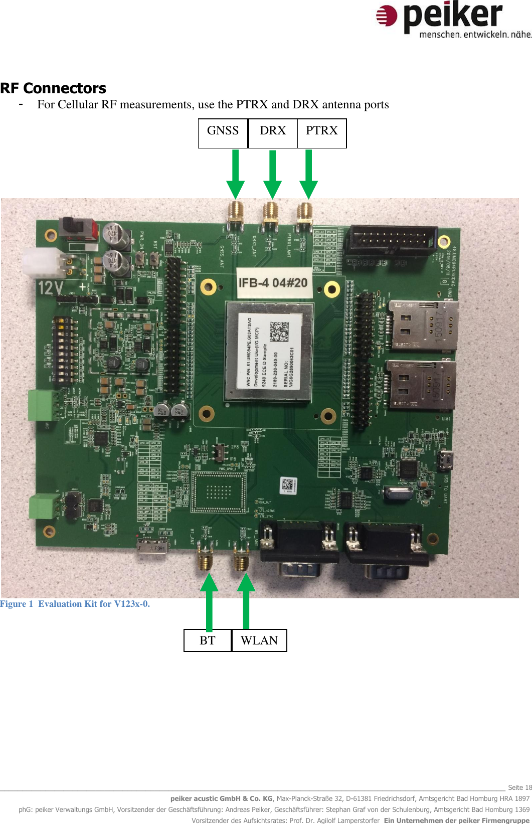
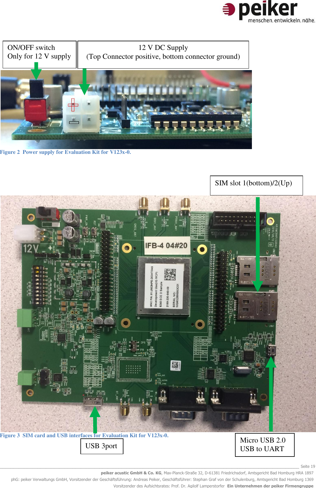
VALEO Telematik und Akustik V1233-0 GSM/WCDMA/LTE Telematics ROW Module User Manual

Peiker acustic GmbH & Co. KG GSM/WCDMA/LTE Telematics ROW Module

User manual

  _______________________________________________________________________________________________________________ Seite 1 peiker acustic GmbH & Co. KG, Max-Planck-Straße 32, D-61381 Friedrichsdorf, Amtsgericht Bad Homburg HRA 1897 phG: peiker Verwaltungs GmbH, Vorsitzender der Geschäftsführung: Andreas Peiker, Geschäftsführer: Stephan Graf von der Schulenburg, Amtsgericht Bad Homburg 1369 Vorsitzender des Aufsichtsrates: Prof. Dr. Agilolf Lamperstorfer  Ein Unternehmen der peiker Firmengruppe    V123x-0 (LTE-NAD-A) User manual              Peiker product IDs:    2189-230-042-00 (V1230-0)  2189-231-042-00 (V1231-0) 2189-232-042-00 (V1232-0)          2189-233-042-00 (V1233-0)               Revision:      1.4 Date:        August 2017
  _______________________________________________________________________________________________________________ Seite 2 peiker acustic GmbH & Co. KG, Max-Planck-Straße 32, D-61381 Friedrichsdorf, Amtsgericht Bad Homburg HRA 1897 phG: peiker Verwaltungs GmbH, Vorsitzender der Geschäftsführung: Andreas Peiker, Geschäftsführer: Stephan Graf von der Schulenburg, Amtsgericht Bad Homburg 1369 Vorsitzender des Aufsichtsrates: Prof. Dr. Agilolf Lamperstorfer  Ein Unternehmen der peiker Firmengruppe    Revision History  Date Revision Name Comment 28.02.2017 1.0 mgi Initial document based on V123x-1 documents 01.03.2017 1.1 phse Some rewording as well as some corrections 06.03.2017 1.2 mgi Model name changed to V123x-0 08.08.2017 1.3 phse Renumbering of some sections Added new section called “Maximum TX Output Power” 04.09.2017 1.4 phse Updated the temp range table from section 2.12.1 Reworked section 6   Updated the pin-out table
  _______________________________________________________________________________________________________________ Seite 3 peiker acustic GmbH & Co. KG, Max-Planck-Straße 32, D-61381 Friedrichsdorf, Amtsgericht Bad Homburg HRA 1897 phG: peiker Verwaltungs GmbH, Vorsitzender der Geschäftsführung: Andreas Peiker, Geschäftsführer: Stephan Graf von der Schulenburg, Amtsgericht Bad Homburg 1369 Vorsitzender des Aufsichtsrates: Prof. Dr. Agilolf Lamperstorfer  Ein Unternehmen der peiker Firmengruppe Content 1 Introduction .......................................................................................................................................... 4 1.1 Scope .................................................................................................................................................. 4 1.2 Audience ............................................................................................................................................ 4 1.3 Contact information, Support ......................................................................................................... 4 2 Product Overview ................................................................................................................................ 5 2.1 Product Variants ................................................................................................................................ 5 2.2 Supported Technology/Frequency Bands ..................................................................................... 5 2.3 Maximum TX Output Power ............................................................................................................ 5 2.5 Features ............................................................................................................................................. 6 2.6 Certifications / Approvals................................................................................................................. 7 2.8 Connectors ......................................................................................................................................... 7 2.8.1 Module Signal and RF Connectors .......................................................................................... 7 2.8.2 Ground and Heat Dissipation Connectors .............................................................................. 7 2.9 Main Interfaces ................................................................................................................................. 8 2.9.1 USB .............................................................................................................................................. 8 2.9.2 SIM Interface ............................................................................................................................. 8 2.9.3 Power on ..................................................................................................................................... 8 2.9.4 Reset ........................................................................................................................................... 8 2.9.5 GPIOs .......................................................................................................................................... 9 2.9.6 GSBIs ........................................................................................................................................... 9 2.9.7 Module Pin-out ......................................................................................................................... 10 2.10 Supply Voltage .............................................................................................................................. 15 2.11 Power Consumption ..................................................................................................................... 15 2.12 Environmental Specification ........................................................................................................ 16 2.12.1 Temperature Range .............................................................................................................. 16 3 Evaluation Kit ..................................................................................................................................... 17 4 AT Command interface ..................................................................................................................... 20 5 Safety Recommendations according to EN60950-1 ..................................................................... 22 6  RED/FCC/IC Regulatory Notices ...................................................................................................... 23 6.1 Modifications .............................................................................................................................. 23 6.2 Interference ................................................................................................................................ 23 6.3 FCC Class B Digital Device ....................................................................................................... 23 6.3 OEM Responsibilities ................................................................................................................. 24 7 List of Acronyms ................................................................................................................................ 25
  _______________________________________________________________________________________________________________ Seite 4 peiker acustic GmbH & Co. KG, Max-Planck-Straße 32, D-61381 Friedrichsdorf, Amtsgericht Bad Homburg HRA 1897 phG: peiker Verwaltungs GmbH, Vorsitzender der Geschäftsführung: Andreas Peiker, Geschäftsführer: Stephan Graf von der Schulenburg, Amtsgericht Bad Homburg 1369 Vorsitzender des Aufsichtsrates: Prof. Dr. Agilolf Lamperstorfer  Ein Unternehmen der peiker Firmengruppe 1  Introduction  1.1 Scope This document gives an overview about electrical, mechanical and functional details of the peiker LTE-NAD-A V123x-0 modules. 1.2 Audience Information to integrate the module in some other applications.   1.3 Contact information, Support peiker acustic GmbH & Co KG  Max-Planck Street 32 D-61381 Friedrichsdorf / Ts. Germany  http://www.peiker.de info@peiker.de
  _______________________________________________________________________________________________________________ Seite 5 peiker acustic GmbH & Co. KG, Max-Planck-Straße 32, D-61381 Friedrichsdorf, Amtsgericht Bad Homburg HRA 1897 phG: peiker Verwaltungs GmbH, Vorsitzender der Geschäftsführung: Andreas Peiker, Geschäftsführer: Stephan Graf von der Schulenburg, Amtsgericht Bad Homburg 1369 Vorsitzender des Aufsichtsrates: Prof. Dr. Agilolf Lamperstorfer  Ein Unternehmen der peiker Firmengruppe 2  Product Overview 2.1 Product Variants  The LTE-NAD-A module family consists of four regional variants:  Peiker product #          Module configuration 2189-230-042-00 (V1230-0)        ECE configuration 2189-231-042-00 (V1231-0)        NA configuration 2189-232-042-00 (V1232-0)        CHN configuration 2189-233-042-00 (V1233-0)        RoW configuration  2.2 Supported Technology/Frequency Bands  V1230-0  GSM Bands      900MHz and 1800MHz WCDMA Bands  FDD1, FDD3 and FDD8  LTE Bands    eFDD1, eFDD3, eFDD7, eFDD20, eFDD28A, eFDD32 and eTTD38  V1231-0 GSM Bands     850MHz and 1900MHz  WCDMA Bands  FDD2, FDD4 and FDD5  LTE Bands    eFDD2, eFDD4, eFDD5, eFDD7, eFDD12 and eFDD29  V1232-0 GSM Bands     900MHz and 1800MHz WCDMA Bands  FDD1 and FDD8 LTE Bands    eFDD1, eFDD3, eFDD7, eTTD38, eTTD40 and eTTD41  V1233-0  GSM Bands   850MHz, 900MHz, 1800MHz and 1900MHz WCDMA Bands  FDD1, FDD2, FDD3, FDD5, FDD6, FDD8 and FDD19 LTE Bands  eFDD1, eFDD3, eFDD5, eFDD7, eFDD8, eFDD9, eFDD19, eFDD21, eFDD28B and eTTD40  2.3 Maximum TX Output Power  GSM 850 and GSM 900 (PCL=5, 1 UL TS): 34,5 dBm GSM 1800 and GSM 1900 (PCL=5, 1 UL TS): 31,5 dBm  GPRS 850 and GPRS 900 (PCL=5, 4 UL TS): 29 dBm GPRS 1800 and GPRS 1900 (PCL=0, 4 UL TS): 26 dBm  EDGE 850 and EDGE 900 (PCL=8, 4 UL TS): 23 dBm
  _______________________________________________________________________________________________________________ Seite 6 peiker acustic GmbH & Co. KG, Max-Planck-Straße 32, D-61381 Friedrichsdorf, Amtsgericht Bad Homburg HRA 1897 phG: peiker Verwaltungs GmbH, Vorsitzender der Geschäftsführung: Andreas Peiker, Geschäftsführer: Stephan Graf von der Schulenburg, Amtsgericht Bad Homburg 1369 Vorsitzender des Aufsichtsrates: Prof. Dr. Agilolf Lamperstorfer  Ein Unternehmen der peiker Firmengruppe EDGE 1800 and EDGE 1900 (PCL=2, 4 UL TS): 22 dBm  WCDMA (all supported frequency bands): 25 dBm LTE (all supported frequency bands): 25 dBm  2.4 Module to Hosts Mapping The below table shows the mapping between the module variants and the host/ATM-02 devices:  Module Host devices embedding this module variant   V1230-0 ATM-02-ECE-R1 and ATM-02-ECE-T1 V1231-0 ATM-02-US-R1 and ATM-02-US-T1 V1232-0 ATM-02-CHN-R1 and ATM-02-CHN-T1 V1233-0 ATM-02-ROW-R1 and ATM-02-ROW-T1  2.5 Features  Features - Same footprint and pin-out (all modules) - Voice and data calls (all modules) - IMS/VoLTE  - 4G: Rel-11, 3G/3G+: Rel-9, 2G: Rel-9 - DTM/eDTM (all modules) - Standalone GPS, GLONASS, Galileo, SBAS, QZSS and BeiDou  Data rates - GPRS/EDGE: Multislot class 33   - WCDMA: DL /UL up to 384kbps  HSPA+: Category 24 in DL using 64 QAM and Dual-Cell; Up to 42 Mbps (All modules except V1231-0)    Category 14 in DL using 64 QAM; Up to 21 Mbps (V1231-0)  Category 6 in UL using 16 QAM; Up to 5.76 Mbps (All modules) - LTE Category 11: Up to 450 Mbps in DL using 3 CCs, up to 75 Mbps in UL (All modules)  Power Classes   - LTE: All supported bands,  Power Class 3  - WCDMA: All supported bands,  Power Class 3   - EDGE:  850/900/1800/1900,  Power Class E2  - GSM/GPRS: 850/900,  Power Class 4  - GSM/GPRS: 1800/1900,  Power Class 1  Dimension and Weight - Dimensions: 35mm x 38mm x 4,35mm - Weight < 10 grams
  _______________________________________________________________________________________________________________ Seite 7 peiker acustic GmbH & Co. KG, Max-Planck-Straße 32, D-61381 Friedrichsdorf, Amtsgericht Bad Homburg HRA 1897 phG: peiker Verwaltungs GmbH, Vorsitzender der Geschäftsführung: Andreas Peiker, Geschäftsführer: Stephan Graf von der Schulenburg, Amtsgericht Bad Homburg 1369 Vorsitzender des Aufsichtsrates: Prof. Dr. Agilolf Lamperstorfer  Ein Unternehmen der peiker Firmengruppe 2.6 Certifications / Approvals   GCF RED PTCRB FCC/IC AT&T V1230-0 Planned Planned    V1231-0   Planned Planned Planned V1232-0  Planned    V1233-0  Planned  Planned    2.7 HW Features  - Qualcomm X12 LTE, 20nmSoC - MDM9240 Baseband / PMIC: PMD9645 / WTR3925 WTR4905  - Cortex-A7 up to 1.2 GHz  - Modem and low power audio sub systems: QDSP6 processor at up to 850 MHz (turbo) - RPM Resource and power manager: Cortex M3 up to 100 MHz  - 4Gb NAND Flash  - 2Gb LPDDR2 SDRAM - 19.2MHz clock reference - GPS, GLONASS, BeiDou, and Galileo  2.8 Connectors 2.8.1 Module Signal and RF Connectors  LTE-NAD-A has 172 signal pins (2xAA and 2xBB) connector pads with 1.0mm pitch. The signal pads are located close to the board edges.  There are three antenna pads, each collocated by RF GND connectors - Main transmit and receive antenna – pin LGA_PRX_ANT - Diversity antenna for WCDMA respective MIMO antenna for LTE – pin LGA_DRX_ANT_IN - GNSS antenna for both GPS and GLONASS – pin LGA_GPS_DRX_ANT  2.8.2 Ground and Heat Dissipation Connectors  To support the usage of module under complicated thermal conditions, there are a number of large grounded pads in the center of PCB. These pads are dedicated ground pads to transfer heat dissipation to a carrier board.  This should be especially considered by customer designs. A reference design showing landing patterns and PCB stack-up is available on request.
  _______________________________________________________________________________________________________________ Seite 8 peiker acustic GmbH & Co. KG, Max-Planck-Straße 32, D-61381 Friedrichsdorf, Amtsgericht Bad Homburg HRA 1897 phG: peiker Verwaltungs GmbH, Vorsitzender der Geschäftsführung: Andreas Peiker, Geschäftsführer: Stephan Graf von der Schulenburg, Amtsgericht Bad Homburg 1369 Vorsitzender des Aufsichtsrates: Prof. Dr. Agilolf Lamperstorfer  Ein Unternehmen der peiker Firmengruppe 2.9 Main Interfaces  2.9.1 USB  LTE-NAD-A has one USB2.0 OTG high speed (480MBit) compliant interface including the PHY. This IF consists of four signals:  - USB_HS_DP:      USB Data Plus signal - USB_HS_DM      USB Data Minus signal - USB_HS_ID:      USB high-speed data - ID - MDM_VBUS_DET:    USB Voltage Supply  LTE-NAD-A has one USB3.0 high speed (480MBit) compliant interface including the PHY. This IF consists of four signals:  - MDM_USB_SS_RX_P:    USB 3.0 receive – plus - MDM_USB_SS_RX_M    USB 3.0 receive – minus - MDM_USB_SS_TX_P:    USB 3.0 transmit – plus - MDM_USB_SS_TX_M:    USB 3.0 transmit – minus  A dynamic reconfiguration between USB-Host or USB-Device is not foreseen. LTE-NAD-A can be configured to USB-Host or USB-Device by insertion of a resistor on the USB_ID line.  2.9.2 SIM Interface  LTE-NAD-A has two SIM interfaces that are compatible for both 1.8V and 3V SIM Cards. Those IFs consist of the following signals:  VREF_UIM1  /  VREF_UIM2 UIM1_CLK  /  UIM2_CLK UIM1_DETECT  /  UIM2_DETECT UIM1_DATA  /  UIM2_DATA UIM1_RESET  /  UIM2_RESET  The data rate of the SIM IF is up to 4 Mbps, so HW designers should take care of the length and routing of the SIM IF to prevent potential EMC problems.  2.9.3 Power on  The signal PON_1 is used to switch on LTE-NAD-A. As PON_1 is pulled against VMAIN internally, it is recommended to pull this input against GND using an open collector or open drain output only.   2.9.4 Reset PMD_RESIN_N is used to reset LTE-NAD-A. As PMD_RES_IN is pulled against VMAIN internally, it is recommended to pull this input against GND using an open collector or open drain output only.
  _______________________________________________________________________________________________________________ Seite 9 peiker acustic GmbH & Co. KG, Max-Planck-Straße 32, D-61381 Friedrichsdorf, Amtsgericht Bad Homburg HRA 1897 phG: peiker Verwaltungs GmbH, Vorsitzender der Geschäftsführung: Andreas Peiker, Geschäftsführer: Stephan Graf von der Schulenburg, Amtsgericht Bad Homburg 1369 Vorsitzender des Aufsichtsrates: Prof. Dr. Agilolf Lamperstorfer  Ein Unternehmen der peiker Firmengruppe 2.9.5 GPIOs  There are 51 GPIOs available on LTE-NAD-A, some of them being part of the five GSBIs (see next section). They are used for different interfaces (see Table 1 and the following sections). For allocation of GPIOs/GSBIs to different configurations, please contact us.   GPIOs and GSBIs share the same output pins and may not available when used as GSBI configuration.   The following GPIOs do not belong to a GSBI bundle:  GPIO 47, 72, 82, 25, 28, 26, 27, 84, 80, 21, 23, 22, 24, 20, 1, 78, 79, 85, 86, 69, 0, 77, 65, 61, 68, 51, 54, 73, 48, 49, 53.  The following GPIOs belongs to a GSBI bundle: GPIO 2, 3, 4, 5, 6, 7, 8, 9, 10, 11, 12, 13, 14, 15, 16, 17, 18, 19, 29, 30.  2.9.6 GSBIs  Five GSBIs (General Serial Bus Interfaces) are available in total, each of them consisting of four GPIOs. The reference voltage of the GSBIs is 1.8V.   Available signals on GSBI bundles at the board to board connector:  - GSBI1:  GSBI1_0, GSBI1_1, GSBI1_2, GSBI1_3 (GPIO_29, 30, 2, 3) - GSBI2:  GSBI2_0, GSBI2_1, GSBI2_2, GSBI2_3 (GPIO_4, 5, 6, 7) - GSBI3:  GSBI3_0, GSBI3_1, GSBI3_2, GSBI3_3 (GPIO_8, 9, 10, 11) - GSBI4:  GSBI4_0, GSBI4_1, GSBI4_2, GSBI4_3 (GPIO_12, 13, 14, 15) - GSBI5:  GSBI5_0, GSBI5_1, GSBI5_2, GSBI5_3 (GPIO_16, 17, 18, 19)
  _______________________________________________________________________________________________________________ Seite 10 peiker acustic GmbH & Co. KG, Max-Planck-Straße 32, D-61381 Friedrichsdorf, Amtsgericht Bad Homburg HRA 1897 phG: peiker Verwaltungs GmbH, Vorsitzender der Geschäftsführung: Andreas Peiker, Geschäftsführer: Stephan Graf von der Schulenburg, Amtsgericht Bad Homburg 1369 Vorsitzender des Aufsichtsrates: Prof. Dr. Agilolf Lamperstorfer  Ein Unternehmen der peiker Firmengruppe 2.9.7 Module Pin-out Table 1  Module Pin-out Pin number Category 9x40 Pin name Description 1 GND GND Ground 2 USB3.0 MDM_USB_SS_TX_M USB 3.0 transmit – minus 105 USB3.0 MDM_USB_SS_TX_P USB 3.0 transmit – plus  3 GND GND Ground 106 GND GND Ground 4 USB3.0 (9x40)  MDM_USB_SS_RX_M USB 3.0 receive – minus  107 USB3.0 (9x40)  MDM_USB_SS_RX_P USB 3.0 receive – plus 5 GND GND Ground 108 GND GND Ground 6 PCIE/WLAN IF PCIE_REFCLK_M PCIe reference clock – minus 109 PCIE/WLAN IF  PCIE_REFCLK_P PCIe reference clock – plus  7 GND GND Ground 110 GND GND Ground 8 PCIE/WLAN IF PCIE_TX_M PCIe transmit – minus   111 PCIE/WLAN IF PCIE_TX_P PCIe transmit – plus  9 GND GND Ground 112 GND GND Ground 10 PCIE/WLAN IF PCIE_RX_M PCIe receive – minus   113 PCIE/WLAN IF PCIE_RX_P PCIe receive – plus   11 GND GND Ground 114 GND GND Ground 12 USB PMD_USB_ID USB high-speed data – ID 115 USB USB2_EXT_VBUS_DET External USB Vbus detection 13 GND GND Ground 116 GPIO GPIO_86 Configurable I/O 14 Reserved  Reserved Inter-chip communication 117 GND GND Ground 15 Reserved  Reserved Inter-chip communication 118 GND GND Ground 16 USB MDM_USB_HS_DP USB high-speed data – plus 119 USB MDM_USB_HS_DM USB high-speed data – minus 17 GND GND Ground
  _______________________________________________________________________________________________________________ Seite 11 peiker acustic GmbH & Co. KG, Max-Planck-Straße 32, D-61381 Friedrichsdorf, Amtsgericht Bad Homburg HRA 1897 phG: peiker Verwaltungs GmbH, Vorsitzender der Geschäftsführung: Andreas Peiker, Geschäftsführer: Stephan Graf von der Schulenburg, Amtsgericht Bad Homburg 1369 Vorsitzender des Aufsichtsrates: Prof. Dr. Agilolf Lamperstorfer  Ein Unternehmen der peiker Firmengruppe 120 SDIO IF/eMMC  GPIO_96 / MDM_SDC1_DATA_4 Secure digital controller data bit 4 18 SDIO IF/eMMC   GPIO_97 / MDM_SDC1_DATA_5 Secure digital controller data bit 5 121 SDIO IF/eMMC  GPIO_98 / MDM_SDC1_DATA_6 Secure digital controller data bit 6 19 SDIO IF/eMMC  GPIO_99 / MDM_SDC1_DATA_7 Secure digital controller data bit 7 122 SDIO IF GPIO_81 / SD_CARD_DET_N Secure digital card detection 20 SDIO IF  MDM_SDC1_DATA_0 Secure digital controller data bit 0 123 SDIO IF  MDM_SDC1_DATA_1 Secure digital controller data bit 1 21 SDIO IF  MDM_SDC1_DATA_2 Secure digital controller data bit 2 124 SDIO IF  MDM_SDC1_DATA_3 Secure digital controller data bit 3 22 GND GND Ground 125 SDIO IF MDM_SDC1_CMD Secure digital controller 2 command 23 SDIO IF MDM_SDC1_CLK Secure digital controller 2 clock 126 SIM1 VREG_L11_UIM1 Reference for UIM I/O pads 24  GND Ground 127 SIM1 GPIO_79 / MDM_UIM1_CLK UIM1 clock  25 SIM1 GPIO_78 /MDM_UIM1_RESET UIM1 reset 128 SIM1 GPIO_77 / MDM_UIM1_DETECT UIM1 detect (non dual voltage) 26 SIM1 GPIO_76 /MDM_UIM1_DATA UIM1 data 27 GND GND Ground 28 I2S GPIO_15 /  I2S_CLK I2S Data Clock 129 GND GND Ground 29 I2S MDM_MCLK Audio Master clock 130 GND GND Ground 30 I2S GPIO_12 / I2S_WS I2S word select 131 I2S GPIO_13 / I2S_DO I2S Data Output 31 I2S GPIO_14 / I2S_DI I2S Data Input  132 GND GND Ground 32  GPIO_19 / ANT_SW_2 Antenna switch 2 133  GPIO_18 / ANT_SW_1 Antenna switch 1 33 UART4 GPIO_17 / UART4_RX UART4 receive data 134 UART4 GPIO_16 / UART4_TX UART4 transmit data 34 GND GND Ground 135 GND GND Ground 35 GPIO  GPIO_50 Configurable I/O 136  GPIO_23 / ANT_SW_4 Antenna switch 4 36 GND GND Ground 137 GND GND Ground 37  MDM_RESOUT_N  138  GPIO_22 / ANT_SW_3 Antenna switch 3
  _______________________________________________________________________________________________________________ Seite 12 peiker acustic GmbH & Co. KG, Max-Planck-Straße 32, D-61381 Friedrichsdorf, Amtsgericht Bad Homburg HRA 1897 phG: peiker Verwaltungs GmbH, Vorsitzender der Geschäftsführung: Andreas Peiker, Geschäftsführer: Stephan Graf von der Schulenburg, Amtsgericht Bad Homburg 1369 Vorsitzender des Aufsichtsrates: Prof. Dr. Agilolf Lamperstorfer  Ein Unternehmen der peiker Firmengruppe 38 UART1 GPIO_21 / UART1_RX  UART1 receive data 139 UART1 UART1_TX UART2 transmit data 39 GND GND Ground 140 SPI GPIO_7 / SPI_CLK SPI clock 40 SPI GPIO_6 / SPI_CS_N SPI chip select 141 SPI GPIO_5 / SPI_MISO SPI master-in slave-out 41 SPI GPIO_4 / SPI_MOSI SPI master-out slave-in 142 SIM2 GPIO_2 / MDM_UIM2_RESET UIM2 reset 42 SIM2 GPIO_1 /MDM_UIM2_DETECT UIM2 detect (non dual voltage) 143 SIM2 GPIO_0 /MDM_UIM2_DATA UIM2 data 43 GND GND Ground 144 SIM2 VREG_L13_UIM2 Reference for UIM I/O pads 44 SIM2 GPIO_3 / MDM_UIM2_CLK UIM2 clock 145 GND GND Ground 45 GND GND Ground 146 GPIO GPIO_94 Configurable I/O 46 GPIO GPIO_80 Configurable I/O 147 GPIO GPIO_90 Configurable I/O 47 GPIO GPIO_82 Configurable I/O 148 GPIO GPIO_91 Configurable I/O 48 GPIO GPIO_87 Configurable I/O 149 GPIO GPIO_92 Configurable I/O 49 GPIO GPIO_88 Configurable I/O 150 GPIO GPIO_93 Configurable I/O 50 GPIO GPIO_89 Configurable I/O 151 I2C GPIO_85 / I2C_SCL I2C clock 51 I2C GPIO_84 / I2C_SDA I2C data 152 GND GND Ground 52 GND GND Ground 53 GND GND Ground 54 GND GND Ground 153 GND GND Ground 55 RF ANT_PTRX1 Primary cellular signal input/output  154 GND GND Ground 56 GND GND Ground 155 GND GND Ground 57 GND GND Ground 156 GND GND Ground 58 GND GND Ground
  _______________________________________________________________________________________________________________ Seite 13 peiker acustic GmbH & Co. KG, Max-Planck-Straße 32, D-61381 Friedrichsdorf, Amtsgericht Bad Homburg HRA 1897 phG: peiker Verwaltungs GmbH, Vorsitzender der Geschäftsführung: Andreas Peiker, Geschäftsführer: Stephan Graf von der Schulenburg, Amtsgericht Bad Homburg 1369 Vorsitzender des Aufsichtsrates: Prof. Dr. Agilolf Lamperstorfer  Ein Unternehmen der peiker Firmengruppe 157 GND GND Ground 59 MIPI GPIO_46 / RFFE4_DATA RF front end 4 interface data 158 GND GND Ground 60 GND GND Ground 159 GND GND Ground 61 MIPI GPIO_47 /RFFE4_CLK RF front end 4 interface clock 160 GND GND Ground 62 GND GND Ground 63 GND GND Ground 162 JTAG MDM_JTAG_TDI JTAG data input 64 GND GND Ground 163 JTAG MDM_JTAG_TDO JTAG data output 65 GND GND Ground 164 JTAG MDM_JTAG_TMS JTAG mode select input 66 GND GND Ground 165 JTAG MDM_JTAG_TRST_N JTAG reset 67 GND GND Ground 166 JTAG MDM_JTAG_TCK JTAG clock input 68 GND GND Ground 167 JTAG MDM_JTAG_SRST_N JTAG reset for debug 69 GND GND Ground 168 JTAG MDM_JTAG_PS_HOLD Power supply hold signal to PMIC 70 GND GND Ground 169 POWER VREG_L6_1P8 1.8V output 71 GND GND Ground 170 GND GND Ground 72 RF ANT_DRX1 Diversity cellular signal input/output 171 GND GND Ground 73 GND GND Ground 172 GND GND Ground 74 Reserved Reserved Reserved 173 GND GND Ground 75 GND GND Ground 174 GND GND Ground 76 GND GND Ground 175 GND GND Ground 77 GND GND Ground 176 GND GND Ground 78 RF ANT_GNSS GNSS signal input/output
  _______________________________________________________________________________________________________________ Seite 14 peiker acustic GmbH & Co. KG, Max-Planck-Straße 32, D-61381 Friedrichsdorf, Amtsgericht Bad Homburg HRA 1897 phG: peiker Verwaltungs GmbH, Vorsitzender der Geschäftsführung: Andreas Peiker, Geschäftsführer: Stephan Graf von der Schulenburg, Amtsgericht Bad Homburg 1369 Vorsitzender des Aufsichtsrates: Prof. Dr. Agilolf Lamperstorfer  Ein Unternehmen der peiker Firmengruppe 79 GND GND Ground 80  GPIO_38 / GRFC12  177 GND GND Ground 81 GPIO GPIO_69 Configurable I/O 178  GPIO_67 / EBI2_AD2/FBS_1  82 GND GND Ground 179 BOOT CONFIG GPIO_36 / FORCED_USB_BOOT Force USB boot control 83 GPIO GPIO_8 Configurable I/O 180 GPIO GPIO_83 Configurable I/O 84 GPIO GPIO_9 Configurable I/O 181  GPIO_59 / NC  85 GND GND Ground 182  GPIO_24 / EBI2_AD1/FBS_0  86 GPIO GPIO_10 Configurable I/O 183  MDM_MODE_0 TBD 87 GPIO GPIO_11 Configurable I/O 184  MDM_MODE_1 TBD 88 GND GND Ground 185 PCIE GPIO_65 / MDM_PCIE_WAKE_N PCIe host wake  89 Reserved Reserved Reserved 186 PCIE GPIO_61 / MDM_PCIE_RESET_N PCIe host reset 90 GND GND Ground 187 PCIE GPIO_64 / MDM_PCIE_CLKREQ_N PCIe clock request 91 GND GND Ground 188 WLAN IF WLAN_PWR_REQ  92 GND GND Ground 189 GPIO  GPIO_60 Configurable I/O 93 WLAN IF WLAN_PWR_EN Enable WLAN Power 190 GPIO  GPIO_68 Configurable I/O 94 WLAN IF WLAN_SLP_CLK  191 BT IF  BT_RESET_N  Enable Bluetooth 95 Power-reset PMIC (active low) PMD_RESIN_N Reset module 192 GND GND Ground 96 Power-on PMIC (active high) PON_1 Turn on module 193 WLAN IF GPIO_95 / WLAN_EN Enable WLAN 97  CBL_PWR_N  194 WLAN IF GPIO_52 / COEX_UART_TX UART transmit data
  _______________________________________________________________________________________________________________ Seite 15 peiker acustic GmbH & Co. KG, Max-Planck-Straße 32, D-61381 Friedrichsdorf, Amtsgericht Bad Homburg HRA 1897 phG: peiker Verwaltungs GmbH, Vorsitzender der Geschäftsführung: Andreas Peiker, Geschäftsführer: Stephan Graf von der Schulenburg, Amtsgericht Bad Homburg 1369 Vorsitzender des Aufsichtsrates: Prof. Dr. Agilolf Lamperstorfer  Ein Unternehmen der peiker Firmengruppe 98 MPP PMIC_MPP_4 Multipurpose Pin 195 WLAN IF GPIO_53 / COEX_UART_RX UART receive data 99 MPP PMIC_MPP_2 Multipurpose Pin 196 MPP PMIC_MPP_6 Multipurpose Pin 100 GND GND_TO_VPH Ground 197 GND GND_TO_VPH Ground 101 POWER VPH_POWER External supply voltage 198 POWER VPH_POWER External supply voltage 102 POWER VPH_POWER External supply voltage 199 POWER VPH_POWER External supply voltage 103 POWER GND_TO_VPH Ground 200 GND GND Ground 104  HW_REV_RESISTOR   Note:  Pins should be grounded when not used in design.  2.10 Supply Voltage  Absolute minimum/maximum supply voltages 3.9V ~ 4.1V Nominal supply voltage 4V Recommended supply voltage 4V Voltage drop @ GSM power burst (33dBm) <100mV  During Hi RF Power GSM bursts the power amplifier can draw peak currents > 2Amps at VMAIN. The voltage drop during the GSM burst shall not exceed 100mV.  2.11 Power Consumption  TA = +25°C, VPH_PWR =3.8V   Output Power Output Power   max. (typ. 23dBm) 0 dBm Voice call WCDMA BC1  ~530mA ~145mA Voice call WCDMA BC2  ~570mA ~145mA Voice call WCDMA BC5  ~630mA ~140mA Voice call WCDMA BC8  ~580mA ~140mA       PCL 5 (typ. 32.5 dBm) PCL 19 (typ. 5dBm) Voice call GSM850   ~260mA ~65mA Voice call GSM900  ~270mA ~65mA   PCL 0 (typ.30.5dBm) PCL 15 (typ.0dBm) Voice call GSM1800  ~165mA ~65mA Voice call GSM1900  ~165mA ~65mA
  _______________________________________________________________________________________________________________ Seite 16 peiker acustic GmbH & Co. KG, Max-Planck-Straße 32, D-61381 Friedrichsdorf, Amtsgericht Bad Homburg HRA 1897 phG: peiker Verwaltungs GmbH, Vorsitzender der Geschäftsführung: Andreas Peiker, Geschäftsführer: Stephan Graf von der Schulenburg, Amtsgericht Bad Homburg 1369 Vorsitzender des Aufsichtsrates: Prof. Dr. Agilolf Lamperstorfer  Ein Unternehmen der peiker Firmengruppe   Output Power Output Power Standby current GSM DRX = 5 Tbd mA  Standby current WCDMA DRX = 7 Tbd mA  Standby current LTE DRX = 7       LTE data call B3    LTE data call B7    LTE data call B20     2.12 Environmental Specification 2.12.1 Temperature Range  Range   Operating temp. range -25°C … +70°C 3GPP spec. conform Extended operating temp. range -40°C … +85°C Note 1 Operational  Performance might slightly deviate from 3GPP spec. Storage temp. range -40°C … +85°C    Note 1: Due to temperature specification of the chipset, the temperature of the power manager and the temperature of the modem chip shall not exceed +85°C.
  _______________________________________________________________________________________________________________ Seite 17 peiker acustic GmbH & Co. KG, Max-Planck-Straße 32, D-61381 Friedrichsdorf, Amtsgericht Bad Homburg HRA 1897 phG: peiker Verwaltungs GmbH, Vorsitzender der Geschäftsführung: Andreas Peiker, Geschäftsführer: Stephan Graf von der Schulenburg, Amtsgericht Bad Homburg 1369 Vorsitzender des Aufsichtsrates: Prof. Dr. Agilolf Lamperstorfer  Ein Unternehmen der peiker Firmengruppe 3  Evaluation Kit  There are two types of evaluation boards fitted with the NAD V123x-0 modules:   The IFB-1 board allows to power-supply the module directly with external 4V along with sense signals. This 4V power-supply should be able to deliver 3.5A max.    The IFB-4 board type takes 12V as input voltage, down-converted to 4V by on-board circuitry.       Features:   -  USB 2.0 (micro USB) for USB to UART -  USB 3.0 (micro b)  -  2*SIM card slot -  Audio support with microphone and loudspeaker connectors -  JTAG connector for debug and programming -  5 RF Antenna connector (PTRX,DRX,GNSS,WL,BT) -  2* RS232 for UART 1 & 4
  _______________________________________________________________________________________________________________ Seite 18 peiker acustic GmbH & Co. KG, Max-Planck-Straße 32, D-61381 Friedrichsdorf, Amtsgericht Bad Homburg HRA 1897 phG: peiker Verwaltungs GmbH, Vorsitzender der Geschäftsführung: Andreas Peiker, Geschäftsführer: Stephan Graf von der Schulenburg, Amtsgericht Bad Homburg 1369 Vorsitzender des Aufsichtsrates: Prof. Dr. Agilolf Lamperstorfer  Ein Unternehmen der peiker Firmengruppe  RF Connectors - For Cellular RF measurements, use the PTRX and DRX antenna ports         Figure 1  Evaluation Kit for V123x-0.          GNSS DRX PTRX BT WLAN
  _______________________________________________________________________________________________________________ Seite 19 peiker acustic GmbH & Co. KG, Max-Planck-Straße 32, D-61381 Friedrichsdorf, Amtsgericht Bad Homburg HRA 1897 phG: peiker Verwaltungs GmbH, Vorsitzender der Geschäftsführung: Andreas Peiker, Geschäftsführer: Stephan Graf von der Schulenburg, Amtsgericht Bad Homburg 1369 Vorsitzender des Aufsichtsrates: Prof. Dr. Agilolf Lamperstorfer  Ein Unternehmen der peiker Firmengruppe      Figure 2  Power supply for Evaluation Kit for V123x-0.      Figure 3  SIM card and USB interfaces for Evaluation Kit for V123x-0. 12 V DC Supply (Top Connector positive, bottom connector ground) ON/OFF switch  Only for 12 V supply  USB 3port Micro USB 2.0  USB to UART SIM slot 1(bottom)/2(Up)
  _______________________________________________________________________________________________________________ Seite 20 peiker acustic GmbH & Co. KG, Max-Planck-Straße 32, D-61381 Friedrichsdorf, Amtsgericht Bad Homburg HRA 1897 phG: peiker Verwaltungs GmbH, Vorsitzender der Geschäftsführung: Andreas Peiker, Geschäftsführer: Stephan Graf von der Schulenburg, Amtsgericht Bad Homburg 1369 Vorsitzender des Aufsichtsrates: Prof. Dr. Agilolf Lamperstorfer  Ein Unternehmen der peiker Firmengruppe  4  AT Command interface  The modules supports standard AT command as listed below.  Commands are compliant to 3GPP TS 27.007 and TS 27.005    Command Description Comment AT+CMGF Message Format  AT+CSCA Service Centre Address  AT+CMGS  Send Message  AT+CGMI  Manufacturer Identification  AT+CGMM  Request model identification  AT+CGMR  Request revision identification  AT+CGSN  Request product serial number  AT+CIMI  Request international mobile subscriber identification  AT+CMOD  Call mode Only one Parameter is supported by the device. AT+CHUP  Hang up call  ATD  Initiate a CS or PS call or supplementary service  ATA Answer incoming CS call command  ATH  Hangup CS call command  AT+CBST  Select bearer service type  AT+CEER  Extended error report  AT+CVHU  Voice hangup control  AT+CREG  Network registration  AT+COPS  PLMN selection  AT+CLCK  Facility lock  AT+CPWD  Change password  AT+CLIP  Calling line identification presentation  AT+CLIR  Calling line identification restriction  AT+CCWA  Call waiting  AT+CHLD  Call related supplementary services  AT+CUSD  Unstructured supplementary service data  AT+CLCC  List current calls  AT+CPOL  Preferred PLMN list  AT+CPAS  Phone active status  AT+CFUN  Set phone functionality  AT+CPIN  Enter PIN  AT+CSQ  Signal quality  AT+CMER  Mobile termination event reporting  AT+CSIM  Generic SIM access  AT+CRSM  Restricted SIM access  AT+CMEE  Report mobile termination error  AT+CGDCONT  Define PDP context  AT+CGEQREQ  Request 3G quality of service profile  AT-CGATT  PS attach or detach  AT+CGACT  PDP context activate or deactivate  AT+CGPADDR  Show PDP address  AT+CGSMS  Select service for MO SMS messages  ATE  Character Echo ON/OFF
  _______________________________________________________________________________________________________________ Seite 21 peiker acustic GmbH & Co. KG, Max-Planck-Straße 32, D-61381 Friedrichsdorf, Amtsgericht Bad Homburg HRA 1897 phG: peiker Verwaltungs GmbH, Vorsitzender der Geschäftsführung: Andreas Peiker, Geschäftsführer: Stephan Graf von der Schulenburg, Amtsgericht Bad Homburg 1369 Vorsitzender des Aufsichtsrates: Prof. Dr. Agilolf Lamperstorfer  Ein Unternehmen der peiker Firmengruppe Command Description Comment    AT+CSMS  Check Message Service support  AT+CSMP  Set Text Mode Parameters  AT+CSDH  Show Text Mode Parameters  AT+CSCB  Select Cell Broadcast Message Types  AT+CSAS  Save Settings Only one Parameter is supported by the device. AT+CRES  Restore Settings Only one Parameter is supported by the device. AT+CMGL  List messages  AT+CNMA  New message acknowledgement  AT+CMGC  Send Command  AT+CMMS  More Messages to Send  AT+ATV  DCE response format  AT+ATX  Result code selection and call progress monitoring control  AT+CNMI  New Message Indications to TE  AT+CPMS  Preferred Message Storage  AT+CMGW  Write Message to Memory  AT+CMSS  Send Message from Storage  AT+CMGD  Delete Messages  AT+CNUM  Get MSISDN  AT+CPBS  Select phonebook memory storage  AT+CPBR  Read phonebook entries  AT+CPBW  Writephonebook entry
  _______________________________________________________________________________________________________________ Seite 22 peiker acustic GmbH & Co. KG, Max-Planck-Straße 32, D-61381 Friedrichsdorf, Amtsgericht Bad Homburg HRA 1897 phG: peiker Verwaltungs GmbH, Vorsitzender der Geschäftsführung: Andreas Peiker, Geschäftsführer: Stephan Graf von der Schulenburg, Amtsgericht Bad Homburg 1369 Vorsitzender des Aufsichtsrates: Prof. Dr. Agilolf Lamperstorfer  Ein Unternehmen der peiker Firmengruppe 5  Safety Recommendations according to EN60950-1  The V123x-0 devices must be supplied by a limited power source according to EN 60950-1.   The clearance and creepage distances required by the end product must be withheld when the module is installed.   The cooling of the end product shall not negatively be influenced by the installation of the module.
  _______________________________________________________________________________________________________________ Seite 23 peiker acustic GmbH & Co. KG, Max-Planck-Straße 32, D-61381 Friedrichsdorf, Amtsgericht Bad Homburg HRA 1897 phG: peiker Verwaltungs GmbH, Vorsitzender der Geschäftsführung: Andreas Peiker, Geschäftsführer: Stephan Graf von der Schulenburg, Amtsgericht Bad Homburg 1369 Vorsitzender des Aufsichtsrates: Prof. Dr. Agilolf Lamperstorfer  Ein Unternehmen der peiker Firmengruppe 6   RED/FCC/IC Regulatory Notices   6.1  Modifications   WARNING:  peiker acustic GmbH & Co. KG has not approved any changes or modifications to the V123x-0 device by the user. Any changes or modifications could void the user’s authority to operate the equipment.  6.2  Interference  V1231-0 and V1233-0 devices comply with Part 15 of the FCC rules. Operation is subject to the following two conditions: (1) Those devices may not cause harmful interference, and (2) Those devices must accept any interference received, including interference that may cause undesired operation.  V1231-0 is a Class b digital apparatus compliant with Canadian ICES-003. V1231-0 est un appareil numérique de la classe b conforme à la norme NMB-003 du Canada.  V1231-0 est conforme aux CNR d'Industrie Canada applicables aux appareils radio exempts de licence. L'exploitation est autorisée aux deux conditions suivantes : (1) l'appareil ne doit pas produire de brouillage, et (2) l'utilisateur de l'appareil doit accepter tout brouillage radioélectrique subi, même si le brouillage est susceptible d'en compromettre le fonctionnement.  6.3  FCC Class B Digital Device  V1231-0 has been tested and found to comply with the limits for a Class B digital device, pursuant to part 15 of the FCC Rules. These limits are designed to provide reasonable protection against harmful interference in a residential installation. This equipment generates, uses, and can radiate radio frequency energy and, if not installed and used in accordance with the instructions, may cause harmful interference to radio communications. However, there is no guarantee that interference will not occur in a particular installation. If this equipment does cause harmful interference to radio or television reception, which can be determined by turning the equipment off and on, the user is encouraged to try to correct the interference by one or more of the following measures:  - Reorient or relocate the receiving antenna. - Increase the separation between the equipment and receiver. - Connect the equipment into an outlet on a circuit different from that to which the receiver is connected. - Consult the dealer or an experienced radio/TV technician for help.
  _______________________________________________________________________________________________________________ Seite 24 peiker acustic GmbH & Co. KG, Max-Planck-Straße 32, D-61381 Friedrichsdorf, Amtsgericht Bad Homburg HRA 1897 phG: peiker Verwaltungs GmbH, Vorsitzender der Geschäftsführung: Andreas Peiker, Geschäftsführer: Stephan Graf von der Schulenburg, Amtsgericht Bad Homburg 1369 Vorsitzender des Aufsichtsrates: Prof. Dr. Agilolf Lamperstorfer  Ein Unternehmen der peiker Firmengruppe 6.3  OEM Responsibilities    Antenna   - The systems antenna(s) must be installed such that 20 cm is maintained between the antenna(s) and the body of the user or nearby persons.  - The V123x-0 transmitter must not be co-located or operating in conjunction with any other antenna or transmitter. The preceding statement must be included as a Caution statement in OEM product manuals in order to alert users of FCC RF Exposure compliance.  - Maximum authorized antenna gain: refer to the MPE test reports  Power Supply   - The power supply of the host device embedding a V123x-0 module must fulfill the following requirements:  o Nominal supply voltage: 4V o Operating voltage range: 3.9V – 4.1V o The above operating voltage range MUST never, under any circumstances (including overshoot voltage and voltage drop), be exceeded.      FCC Labeling   Labeling requirements for a host device embedding V1231-0: V1231-0 is labeled with its own FCC ID Number. If the FCC ID is not visible when V1231-0 is installed inside another device, then the host device must contain the FCC ID number with the statement such as the following: "Contains Transmitter Module FCC ID: QWY-V1231-0" or "Contains FCC ID: QWY-V1231-0"  Labeling requirements for a host device embedding V1233-0: V1233-0 is labeled with its own FCC ID Number. If the FCC ID is not visible when V1233-0 is installed inside another device, then the host device must contain the FCC ID number with the statement such as the following: "Contains Transmitter Module FCC ID: QWY-V1233-0" or "Contains FCC ID: QWY-V1233-0"   IC Labeling   Labeling requirements for a host device embedding V1231-0: V1231-0 is labeled with its own IC ID Number. If the IC ID is not visible when V1231-0 is installed inside another device, then the host device must contain the IC ID number with the statement such as the following: "Contains Transmitter Module IC 6588A- V12310" or "Contains IC 6588A- V12310".
  _______________________________________________________________________________________________________________ Seite 25 peiker acustic GmbH & Co. KG, Max-Planck-Straße 32, D-61381 Friedrichsdorf, Amtsgericht Bad Homburg HRA 1897 phG: peiker Verwaltungs GmbH, Vorsitzender der Geschäftsführung: Andreas Peiker, Geschäftsführer: Stephan Graf von der Schulenburg, Amtsgericht Bad Homburg 1369 Vorsitzender des Aufsichtsrates: Prof. Dr. Agilolf Lamperstorfer  Ein Unternehmen der peiker Firmengruppe 7  List of Acronyms  3GPP 3 rd Generation Partnership Project ADC Analog Digital Converter ADN Abbreviated Dialing Number A-GPS CP Assisted GPS Control Plane AMR  Adaptive Multi Rate AT Attention Command AWS Advanced Wireless Services BER Bit Error Rate CLIP Calling Line Identification Presentation CLIR Calling Line Identification Restriction CSD Circuit Switch Data DARP Downlink Advanced Receiver Performance EDGE Enhanced Data rates for GSM Evolution DTMF Dual Tone Multi Frequency FCC Federal Communications Commission FDN Fixed Dialing Number FTP File Transfer Protocol GCF Global Certification Forum GSM Global System for Mobile communication GPIO General Purpose Input Output GPRS General Packet Radio Service GPS Global Positioning System HSPA High Speed Uplink Packet Access HW Hardware IC Industry Canada LED Led Emitting Diode LTE Long-Term Evolution MO Mobile Originated MT Mobile Terminated OEM Original Equipment Manufacturer PCB Printed Circuit Board PCM Pulse Code Modulation PDU Protocol Data Unit PIN Personal Identification Number PTCRB PCS Type Certification Review Board RF Radio Frequency RoHs Restriction of Hazardous Substances UART Universal Asynchronous Receiver and Transmitter USB Universal Serial Bus USIM Universal Subscriber Identity Module UMTS Universal Mobile Telecommunications System WCDMA Wideband Code Division Multiple Access

Navigation menu