Via Technologies Computer Hardware 3301770 Users Manual
2015-02-03
: Via-Technologies Via-Technologies-Computer-Hardware-3301770-Users-Manual-458305 via-technologies-computer-hardware-3301770-users-manual-458305 via-technologies pdf
Open the PDF directly: View PDF ![]() .
.
Page Count: 114 [warning: Documents this large are best viewed by clicking the View PDF Link!]

User’s Manual
3301770

3301770
Revision History
Title 3.5” Embedded Controller
Revision Number Description Date of Issue
1.0 Initial release November 18, 2005
Copyright Notice
The information in this document is subject to change without prior notice in order to improve
reliability, design, and function and does not represent a commitment on the part of the
manufacturer.
In no event will the manufacturer be liable for direct, indirect, special, incidental, or consequential
damages arising out of the use or inability to use the product or documentation, even if advised of
the possibility of such damages.
This document contains proprietary information protected by copyright. All rights are reserved. No
part of this manual may be reproduced by any mechanical, electronic, or other means in any form
without prior written permission of the manufacturer.
Trademarks
VIA and Mark CoreFusion™ are the registered trademarks of VIA Technologies. S3, S3
Corporation logo, and ProSavage4 are registered trademark of S3 Graphics Corporation, Limited.
AMI is a registered trademark of American Megatrends Inc. Other product names mentioned
herein are used for identification purposes only and may be trademarks and/or registered
trademarks of their respective owners.
Page 2
3301770
Table of Contents
Revision History ·························································································································· 2
Copyright Notice·························································································································· 2
Trademarks··································································································································· 2
Table of Contents························································································································· 3
List of Tables ································································································································ 6
List of Figures ······························································································································ 7
CHAPTER 1 INTRODUCTION
Product Overview ·····················································································································1-2
1.1 General Information········································································································1-2
Connectivity ····························································································································1-3
Label ···································································································································1-3
Function··································································································································1-3
1.2 3301770 Board Overview ····················································································1-5
1.3 Technical Specifications ································································································1-6
Audio Connector·····················································································································1-7
AC ’97 interface ······················································································································1-8
Packing List ····························································································································1-8
System Monitoring··················································································································1-8
CHAPTER 2 FUNCTIONAL DESCRIPTION
2.1 CPU, Memory, and VIA Chipsets ···················································································2-2
CPU ············································································································································ 2-2
Memory······································································································································· 2-3
ProSavage4 Technologies·········································································································· 2-3
VGA/LCD Interface ····················································································································· 2-4
System Memory ·························································································································· 2-4
8MB ············································································································································ 2-4
16/32MB ····································································································································· 2-4
Block Diagram ························································································································2-5
Page 3
3301770
Important Features ·················································································································2-6
2.2 External Interfaces··········································································································2-8
Label ·································································································································2-10
Function································································································································2-10
2.2.1 Internal Connectors ······································································································ 2-11
2.2.2 Front Panel Connectors ·······························································································2-31
CHAPTER 3 INSTALLATION
3.1 Considerations Prior to Installation ··············································································3-2
Preparing Your Embedded Board···························································································3-2
Installation Notices ·················································································································3-2
Airflow Consideration ·············································································································3-3
Unpacking Precautions ··········································································································3-3
Approved Memory Modules ···································································································3-3
3.2 Mechanical Diagrams ·····································································································3-4
3.3 Jumper Settings ··············································································································3-5
JP1 (Clear CMOS) ·················································································································3-6
JP1 Pin Configuration·············································································································3-6
JP1 ···································································································································3-6
JP2: COM2 Serial Port Operation Mode Selector··································································3-7
JP3: COM2 Signal Selector····································································································3-7
3.4 Installation ·······················································································································3-8
IDE Disk Drive and CDROM Connector (IDE0) ·····································································3-8
Optional Floppy Drive Connector (FDD1) ··············································································3-9
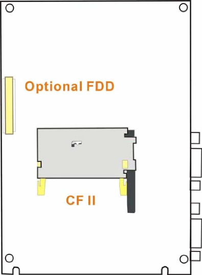
Compact Flash Disk ···············································································································3-9
Parallel Port Connector (CN15)······························································································3-9
Audio Interface ·····················································································································3-10
COM Port Connectors [COM1(CN22), COM2(CN16)]·························································3-10
LCD Panel Connection (CN26, CN28, and CN29) ······························································3-10
Ethernet Connection (CN20 & CN21) ·················································································· 3-11
USB Connection (CN24 and CN19) ·····················································································3-12
Accessories Included in Kit ··································································································3-13
Page 4
3301770
CHAPTER 4 AMI BIOS SETUP
Introduction ·······························································································································4-2
Starting Setup ···························································································································4-2
Using Setup ·······························································································································4-2
Getting Help ······························································································································4-3
4.1 Setup Summary···············································································································4-4
4.2 Main Menu Selections ····································································································4-5
4.3 Standard CMOS Setup Selections·················································································4-5
4.4 Advanced CMOS Setup Selections ··············································································4-7
4.5 Advanced Chipset Setup Selections ·········································································· 4-11
4.6 Power Management Setup Selections ·······································································4-13
4.7 PCI / Plug and Play Setup Selections ········································································4-15
4.8 Peripheral Setup Selections························································································4-17
4.9 Hardware Monitor Setup Selections ···········································································4-19
4.10 Auto-Detect Hard Drives ······························································································4-19
APPENDIX A WATCHDOG TIMER
APPENDIX B CONNECTING ATX POWER SUPPLY
1. Using ATX Power Switch ································································································ B-2
2. Using AT Power Supply ·································································································· B-3
APPENDIX C ALI
®
RAID FOR SATA
1. Introduction························································································································ C-2
Precautions ···························································································································: C-2
2. Features and Benefits ······································································································· C-3
3. SATA-ALi RAID Driver ······································································································· C-4
4. Accessing the ALi RAID Utility··························································································· C-6
Page 5
3301770
List of Tables
Table 1-1 Technical Specifications ........................................................................6
Table 2-1 Supported CRT and Panel Screen Resolutions....................................4
Table 2-2 Important Features ................................................................................6
Table 2-3 Interface Connectors ...........................................................................10
Table 2-4 CN1: Power 4P Connector .................................................................. 11
Table 2-5 CN2 SBVCC: ATX Power Feature Pinouts .........................................13
Table 2-6 CN3 IVTC Inverter Control Pinouts .....................................................13
Table 2-7 CN4 Fan Connector ............................................................................13
Table 2-8 CN5 Pinouts ........................................................................................14
Table 2-9 CN8 Audio Pinouts ..............................................................................15
Table 2-10 CN9 Audio CD_IN Pinouts ..................................................................16
Table 2-11 PC/104-64 Connector Pinouts ............................................................16
Table 2-12 PC/104-40 Connector Pinouts ............................................................17
Table 2-13 CN11 -VCC PC/104 Supplementary Power ........................................18
Table 2-14 CN12 Reset Button Connector Pinouts ..............................................19
Table 2-15 CN13 Power ON/OFF Button Connector Pinouts ...............................19
Table 2-16 CN14 Digital I/O Connector Pinouts....................................................20
Table 2-17 Digital I/Os to Southbridge Reference Chart.......................................20
Table 2-18 CN15 Parallel Port Pinouts .................................................................21
Table 2-19 COM2: 14 (2x7) Pin 2.0mm Connector Pinouts..................................22
Table 2-20 CN17 Keyboard/Mouse Header Pinouts .............................................23
Table 2-21 Serial ATA Port Pinouts .......................................................................24
Table 2-22 CN24 USB Port Pinouts ......................................................................25
Table 2-23 CN27 IrDA Interface Port Pinouts .......................................................25
Table 2-24 CN28 Flat Panel Connector Pinouts ...................................................26
Table 2-25 CN29 LVDS Connector Pinouts ..........................................................27
Table 2-26 CN30 IDE Connector Pinouts .............................................................28
Table 2-27 CN31: Optional Floppy Connector ......................................................29
Table 2-28 CN32 Pinouts ......................................................................................30
Table 2-29 Ethernet Port Pinouts ..........................................................................31
Table 2-30 Ethernet Port LED Indications.............................................................32
Table 2-31 Serial Port COM1 Pinouts ...................................................................32
Table 2-32 VGA Port Pinouts ................................................................................32
Table 3-1 JP1 Pin Configuration ...........................................................................6
Page 6
3301770
Table 3-2 JP2 Pinouts ...........................................................................................7
Table 3-3 JP3 COM2 Signal Selector ...................................................................7
Table 3-4 Cables and Accessories Included in Kit ..............................................13
Table 4-1 BIOS Function Keys ..............................................................................2
Table A-1 I/O Ports to Watchdog Timer .................................................................2
Table A-2 Watchdog Timer Output Data................................................................2
List of Figures
Figure 1-1 3301770 Board Layout ................................................................2
Figure 1-2 3301770 Board Overview ............................................................5
Figure 1-3 3301770 Board Overview ............................................................5
Figure 2-1 System Block Diagram ...........................................................................5
Figure 2-2 External Interfaces .................................................................................8
Figure 2-3 Locations of Configuration Jumpers.......................................................9
Figure 2-4 Power 4P Connector ............................................................................12
Figure 2-5 SBVCC ATX Power Feature.................................................................13
Figure 2-6 Inverter Backlight Control .....................................................................13
Figure 2-7 CN4 Fan Connector .............................................................................13
Figure 2-8 CN5 Power and HDD LED Connector .................................................14
Figure 2-9 CN8 Audio Port.....................................................................................15
Figure 2-10 CN9 Audio CD_IN Port.........................................................................16
Figure 2-11 CN11 –VCC Power...............................................................................18
Figure 2-12 CN12 Reset Button Connector.............................................................19
Figure 2-13 CN13 Power ON/OFF Button Connector .............................................19
Figure 2-14 CN14 Digital I/O Connector..................................................................21
Figure 2-15 CN15 Parallel Port................................................................................22
Figure 2-16 COM2 Connector .................................................................................22
Figure 2-17 COM2 Adapter Cable ...........................................................................23
Figure 2-18 CN17 Keyboard/Mouse Pin Header.....................................................24
Figure 2-19 Serial ATA Port......................................................................................24
Figure 2-20 CN24 USB (1.1) Port............................................................................25
Figure 2-21 CN27 IrDA Interface Port .....................................................................25
Figure 2-22 CN28 TFT Panel Display Connector ....................................................26
Figure 2-23 CN29 LVDS Panel Display Connector .................................................27
Page 7
3301770
Figure 2-24 IDE Connector ......................................................................................29
Figure 2-25 CN31 Floppy Port.................................................................................29
Figure 2-26 Front Panel Connectors .......................................................................31
Figure 2-27 10/100BaseT Ethernet (RJ-45) Port.....................................................31
Figure 3-1 Board Dimensions and Mounting Hole Locations ..................................4
Figure 3-3 Locations of Configuration Jumpers.......................................................5
Figure 3-4 JP3 Pin Locations...................................................................................7
Figure 3-5 Soldering Side Sockets ..........................................................................8
Figure 3-7 PXE Central Management ...................................................................12
Figure B-1 ATX Power Connection ..........................................................................2
Figure B-2 ATX Power Adapter Cable......................................................................3
Safety Notice
Electrical shock hazards might occur while proceeding with the installation, repair and
maintenance of this product. Therefore, the following precaution measures should be carefully
observed:
1. All sorts of operations on this product must be carried out by certified technicians.
2. The chassis into which the embedded board and its associated backplane are installed should
provide stable power supply and be properly grounded.
3. Power off the embedded board and unplug its power cord before handling.
4. When handling the embedded board, avoid touching any metal leads or connectors.
5. Please verify that the power supply is switched off before unplugging the power supply
connector from the embedded board.
ESD Precautions
Observe all conventional anti-ESD methods while handling the embedded board. The use of a
grounded wrist strap and an anti-static work pad is recommended. Avoid dust and debris or other
static-accumulating materials in your work area.
Page 8

3301770
Conventions Used in This Manual
WARNING!
Warnings appear where overlooked details may cause damage to the equipment or result in
personal injury. Warnings should be taken seriously. Warnings are easy to recognize.
The word “warning” is written as “WARNING,” both capitalized and bold and is followed by
the warning message.
CAUTION!
Cautionary messages should also be heeded to help you reduce the chance of losing data
or damaging the system. Cautions are easy to recognize. The word “caution” is written as
“CAUTION,” both capitalized and bold and is followed by the cautionary message.
NOTE:
These messages inform the reader of essential but non-critical information. These messages
should be read carefully as any directions or instructions contained therein can help you
avoid making mistakes. Notes are easy to recognize. The word “note” is written as
“NOTE,” both capitalized and bold and is followed by the cautionary message.
Lists
Bulleted Lists: Bulleted lists are statements of non-sequential facts that can be read in any
order. Each statement is preceded by a square or round black dot.
Numbered Lists: Numbered lists describe sequential steps you should follow in order.
Software Updates
Please contact your system vendor for the latest software or BIOS updates. NOTE that the
BIOS version and associated drivers installed on your system should provide the complete
functionality listed in the Datasheet/User Manual.
Page 9
3301770
We provide special revisions for various application purposes. Therefore, DO NOT upgrade
your BIOS unless you fully understand what a revision will do.
Problems that occur during the updating process may cause unrecoverable errors and
system down time. Always consult qualified technicians before proceeding with any
upgrade.
Page 10

3301770
Chapter
1
Introduction
1-1
3301770
Product Overview
1.1 General Information
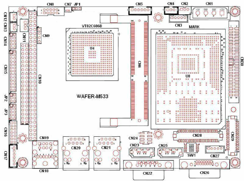
The 3301770 is a highly-integrated embedded computer specifically optimized for
multimedia applications requiring minimum installation space. It supports a full range
of functionality for an AT/ATX-compatible industrial computer in a space-saving 3.5”
profile. The 3301770 is equipped with a low-power consumption and high
performance VIA processor on board. It also contains an SDRAM SODIMM socket
that supports up to 512MB memory in size.
Figure 1-1 3301770 Board Layout
1-2

3301770
Connectivity
The 3301770 provides the following interface connections:
Label Function
CN1 4P power connector
CN2 3-pin PS-ON/ATX feature connector
CN3 5-pin Inverter control
CN4 3-pin CPU fan connector
CN5 5-pin External LED connector (to chassis LED control PCB)
CN6 144-pin SDRAM SO-DIMM socket
CN7 2-pin connector to the external Lithium 3V coin cell battery-
CN8 10-pin audio connector (to the external adapter cable kit which
should provide phone jacks for Line_out, Line_in, and MIC_in
connectivity)
CN9 4-pin Audio CD_IN connector
CN10 PC/104 connector (104-pin ISA bus)
CN11 3-pin external VCC (supplementary for PC/104) power connector
CN12 2-pin Reset button switch (to the chassis front panel)
CN13 2-pin Power switch button (to the chassis front panel)
CN14 10-pin general purpose I/Os connector
CN15 26-pin parallel port pin header
CN16 14-pin internal serial port pin header (COM2)
CN17 6-pin keyboard/mouse connector (a 6-pin-to-PS/2 adapter cable is
required)
CN18 Not implemented
CN19 External USB1.1 connector (2 ports)
CN20 10/100BaseT Ethernet port
CN21 10/100BaseT Ethernet port
CN22 External D-SUB 9 serial port connector (COM1)
CN23 Serial ATA connector
CN24 8-pin internal USB header (an adapter cable required)
CN25 Serial ATA connector
1-3

3301770
CN26 D-SUB 15-pin VGA connector
CN27 5-pin IrDA connector
CN28 TFT LCD connector (DF13-40P-1.25V)
CN29 LCD panel dual-channel 18-bit LVDS/TTL connector, 30 (2x15) pin
header 1.25mm (DF13-30P-1.25V)
CN30 Primary IDE bus connector (44-pin 2.0mm)
CN31 FDC flat type floppy port (one floppy drive only)
CN32 Compact flash storage card socket
The 3301770 is built around a VIA MARK CoreFusion™ chipset which
combines integrated ProSavage4 Graphics with video controller and VIA
VT82C686B PCI to ISA bridge controller. The VIA MARK enables
high-performance graphics features by the 64-bit processing power and the AGP 4X,
32-bit true color rendering, Anisotropic filtering, single-pass multiple textures,
Specular lighting and diffuse shading, MPEG-2 playback, just to name a few.
The built-in ProSavage4 display controller supports both the CRT and LCD display
simultaneously. It offers the resolutions of LCD screen up to 1600 x 1200 pixels,
with 36-bit DSTN/TFT flat panel interface with 256 gray shade support. The
extensive display support for LCD is capable of driving 2-channel 110MHz LVDS
interface with panel power sequencing and hardware suspend/standby control. The
onboard Flash ROM contains both the system BIOS and the VGA BIOS.
Modifications could be done by programming the Flash ROM if necessary.
With a specially designed aluminum heatsink, this board can operate without a
cooling fan at temperatures up to 60° C (140°F) and typically consumes low power
watts while supporting numerous peripherals.
OSes tested and proved compliant include: DOS 6.22, Windows 2000, Windows XP,
Red Hat 9.0, and SuSe 9.0.
1-4
3301770
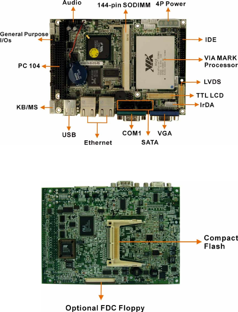
1.2 3301770 Board Overview
Component Side
Figure 1-2 3301770 Board Overview
Soldering Side
Figure 1-3 3301770 Board Overview
1-5

3301770
1.3 Technical Specifications
Table 1-1 Technical Specifications
CPU
Chipset
z
Embedded VIA® Mark CoreFusion Low Voltage processor
at 533MHz
- OR -
z
Embedded VIA® Mark CoreFusion Low Voltage processor
at 800MHz
z
VT82C686B (Northbridge integrated with CPU) with S3 Savage4
3D/2D graphics engine
Memory
z
One 64-bit PC 100/133 144-pin SODIMM socket that supports
SDRAM memory up to 512MB
Display Controller
z
Integrated ProSavage4 w/ 3D/2D/Video controller
z
Supports AGP 4x performance
z
Supports single cycle 128-bit 3D architecture
z
24-bit TTL/dual 18-bit DSTN/TFT flat panel interface
z
Integrated 2-channel 110MHz LVDS interface
z
Support for all resolutions up to 1024X768 pixels
z
Hardware Suspend/Standby control
PCI Interface
z
PCI 2.2 compliant, 32-bit 3.3V PCI interface w/ 5V tolerant
inputs
z
Up to 5 PCI masters
z
PCI to system memory data streaming support
10/100Mbps
Realtek8100C
Ethernet
Controller
z
IEEE 802.3 10/100M Base-T standard auto-sensing interface to
10Mbps or 100Mbps networks through an onboard RJ-45
connector.
BIOS
z
AMI 256KB Flash memory
Compact Flash
Disk
z
Runs in true IDE mode that simulates the operation of a physical
IDE hard drive. It can be used with a passive adapter in a Type
II socket in DMA mode.
IDE Interface
z
Supports one ATA33/66/100 IDE channel with the connectivity
to two hard disk drives
FDD Interface
z
Supports one optional floppy disk drive, 3.5” (720KB or 1.44MB )
by a 26-pin FPC connector cable.
1-6

3301770
Serial Ports
z
Two RS-232 ports with 16C550 UART (or compatible) with
16-byte FIFO buffer. COM2 can support RS-422/485 through
jumper setting.
Parallel Port
z
One parallel port supports SPP/EPP/ECP mode
z
One 2x5 pin header supports AC’97 2.3 Line-in, Line-out, and
Audio Connector
USB Interface
Watchdog Timer
Mic-in signals.
z
Four (4) USB ports, Two external and two internal via pin header;
USB 1.1 compliant.
z
Can be Set to 1 to 255 seconds period. Reset or NMI will be
generated when CPU does not periodically trigger the timer.
PC-104 Interface
z
Direct ISA DMA mode operation.
z
A non-volatile 1Kbit EEPROM is provided to retain application
E2Key
Power Supply
critical read/write data.
z
+5V: 2.58A typical, VIA Mark 533MHz CPU w/ 1x128MB
PC-100/133 module
z
+5V: 2.75A typical, VIA Mark 800MHz CPU w/ 1x128MB
PC-100/133 module
Hardware Monitor
z
System voltage detection
z
CPU temperature detection
IrDA Port
z
Supports Serial Infrared (SIR) and Amplitude Shift Keyed IR
(ASKIR) interface
Operating
Temperature
z
0° to 60°C
Form Factors
z
5.75”(L) x 4”(W) x 1”(H)
1-7

3301770
AC ’97 interface
z
Provides 10 Pin Audio header.
z
16-bit, full-duplex AC'97 Rev. 2.3 compatible six-channel audio
CODEC designed for PC multimedia systems, including host/soft
audio and AMR/CNR-based designs.
„
Meets performance requirements for audio on
PC99/2001 systems
„
Meets Microsoft WHQL/WLP 2.0 audio requirements
„
16-bit Stereo full-duplex CODEC with 48KHz
sampling rate
„
Compliant with AC'97 Rev 2.3 specifications
¾
Front-Out, Surround-Out, MIC-In and LINE-In Jack Sensing
¾
14.318MHz -> 24.576MHz PLL to eliminate crystal
¾
12.288MHz BITCLK input
¾
Integrated PCBEEP generator to save buzzer
¾
Interrupt capability
Packing List
2xSATA cables
1xAudio adapter cable
1x4P-to-SATA power adapter cable
1xIDE flat cable 44p/40p/40p
1xsecond serial port (COM2) cable
1xKeyboard/ PS2 mouse cable
1xMini jumper pack
1xDriver and Utility CD
1xQIG (Quick Installation Guide)
System Monitoring
The 3301770 is capable of self-monitoring various aspects of its operating status:
z
Vcore voltage, +3.3V, +5V, and +2.5V
z
RPM of cooling fans (not implemented with this model)
z
CPU and board temperatures (by the corresponding embedded sensors)
1-8

3301770
Chapter
2
Functional Description
2-1
3301770
This chapter provides a functional description of the 3301770 embedded board designed
for the integration into a compact size chassis. This chapter includes information about
main processors, interface connectors, implementation options, and signal description.
2.1 CPU, Memory, and VIA Chipsets
CPU
The 3301770 comes with a soldered low voltage VIA MARK processor. The VIA MARK CoreFusion
design integrates high-performance ProSavage4 3D/2D graphics controller, LCD and Flat Panel
display interfaces, with the burst and concurrent operation pipelining capability for fast data
distribution among CPU, DRAM, and PCI buses. CPU and the Northbridge functionalities are
provided in a single processor package. The CPU is accompanied by the VT82C686B
Southbridge featuring PC98/PC99 with integrated UltraDMA-66/100 IDE, USB, and a complete
power management feature set. The VT82C686B also provides hardware monitoring, super I/O
functions (floppy disk drive and serial/parallel ports. The AC’97 capabilities are provided by a
Realtek ALC655 chip supporting digital audio output.
The CPU is passively cooled over a heatsink made in aluminum alloy and is ideal for small form
factor computing applications with its low power consumption and minimum heat dissipation.
Shown below are some of the key features of the VIA MARK CoreFusion processor:
z
Integrated ProSavage4 Graphics with VT82C686B PCI-to-ISA bridge controller (352-pin
BGA).
z
Advanced memory controller supporting up to PC133 SDRAM.
z
State-of-the-art power management by the VT82C686B Southbridge.
z
Ideal for applications such as thin client, POS, IPC, STB, PVR, and DVR.
z
533MHz or 800MHz speed options.
z
Eight outstanding transactions (eight level deep In-Order command Queue (IOQ).
z
Built-in Phase Lock Loop circuitry for optimal skew control within and between clocking
regions.
z
Fast AES encryption using the Advanced Cryptography Engine (ACE)
z
Software compatible with thousands of x86 software applications
2-2

3301770
z
Two large (64KB each, 2-way) on-chip caches
z
64KB Level 2 victim cache (16-way)
z
Unique and sophisticated branch prediction mechanisms
Memory
The 3301770 provides one (1) 144-pin SDRAM SODIMM socket without ECC support for
building a buffer size up to 512MB. The memory is automatically identified. The memory
interface supports PC100/133 144-pin SODIMM modules.
ProSavage4 Technologies
„
Integrated with CPU with 2D/3D/Video controllers
„
Optimized Shared Memory Architecture (SMA)
„
Full internal AGP 4x performance
„
Significant internal architecture upgrades from original S3 Savage4 standalone product
„
8/16/32MB frame buffer using system memory
„
Works with VIA VT82C686A/B PCI-to-ISA South Bridge for advanced power
management.
NOTE:
If you need to install VGA driver for the board in a Windows NT environment,
make sure your NT version is later than WinNT40 Server Pack3 or later. The
chipset vendor does not provide S3 VGA driver for earlier NT versions.
The 3301770 is powered by a VIA MARK chipset by VIA Technology Inc. featuring the embedded
AGP/SVGA controller functionalities. It enables the connectivity to many popular LCD,
LVDS LCD displays, and conventional analog CRT monitors. The VIA chipset supports color TFT
LCD flat panel displays. Features also include interlaced and non-interlaced analog monitors
(color and monochrome VGA) in high-resolution modes with the support for complete IBM VGA
compatibility. Digital monitors (namely, MDA, CGA, and EGA) are NOT supported. The
operation with Multiple frequency (multisync) monitors is transparently handled as if they were
analog monitors.
2-3
3301770
VGA/LCD Interface
Chipset: VIA MARK CPU with integrated ProSavage4 2D/3D/Video Accelerator
Frame buffer: Supports 4/8/16/32MB buffer with system memory
Interface: 4X AGP VGA/LCD interface, supports for 18-, 24-bit LVDS or TFT panel
The graphics support includes VGA, SVGA, XGA, and SXGA+ TFT color panels with 9-bit, 12-bit,
18-bit (both 1 pixel/clock and 2 pixels/clock), and 24-bit CMOS interfaces. Enhanced DSTN
hardware with 256 gray scale support, and advanced frame rate control to provide up to 16.7
million colors. In addition, the integrated 2-channel LVDS interface can support 18-bit color
panels. All resolutions are supported up to SXGA+ (1400x1050).
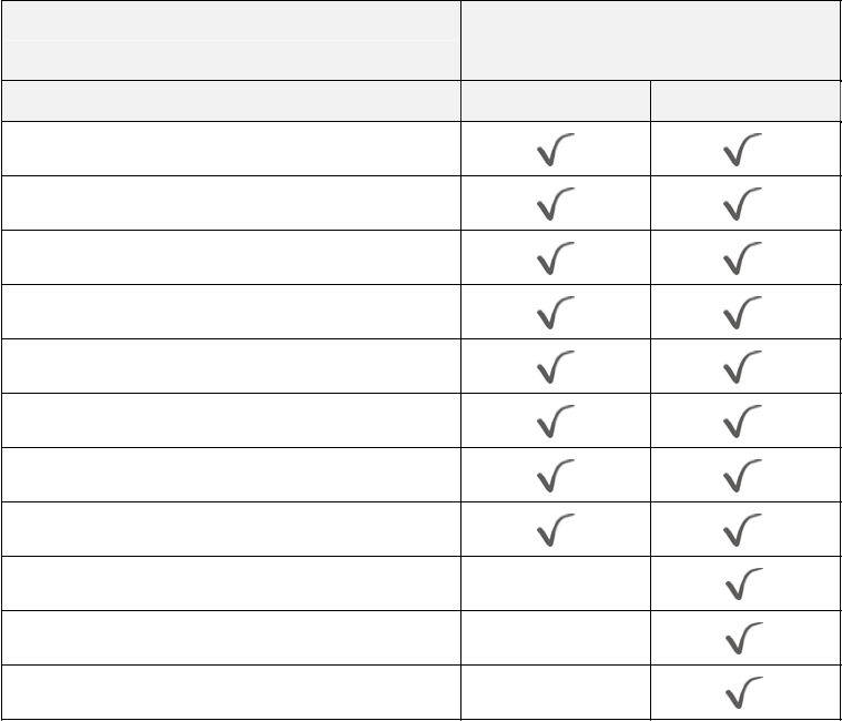
Table 2-1 Supported CRT and Panel Screen Resolutions
System Memory
Frame Buffer Size
Resolutions Supported 8MB 16/32MB
640x480x8/16/32
800x600x8/16/32
1024x768x8/16/32
1280x1024x8
1280x1024x16
1280x1024x32
1600x1200x8
1600x1200x16
1600x1200x32
1920x1440x8
1920x1440x16
2-4
3301770
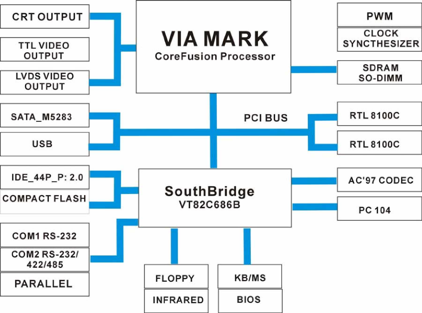
Block Diagram
Figure 2-1 System Block Diagram
2-5

3301770
Important Features
Major functionalities provided by the 3301770 are listed below:
Table 2-2 Important Features
„
RoHS compliance
„
VIA long term support product; embedded VIA processor
„
PC104 PCI-to-ISA extension slot for stack-up configurations
„
CF II socket
„
Embedded ProSavage4 Graphics Controllers with the support for CRT
and LVDS displays
„
Supports one 24-bit TFT, and with up to 1920 x 1440 resolutions
„
Aluminum alloy heatsink for optimum heat dissipation
„
Supports dual-channel 18-bit LVDS and/or 24-bit TFT LCD interface
„
System Memory: one 144-pin SODIMM socket for memory modules
ranging from 64MB to 512MB in size.
„
64KB L2 cache for fast I/O turnarounds
„
Two serial ports, COM1 for RS-232, COM2 for RS-232/422/485
„
One parallel port supports SPP/EPP/ECP modes
„
USB compliant with the USB rev. 1.1 standard
„
System Chipset: VIA MARK CoreFusion + VIA VT82C686B
„
Hardware Monitor: built-in to monitor CPU Vcore, VCC, CPU/System fan
speed, and temperature detection functionalities.
„
Independent DMA audio engines
„
PXE LAN support with ATX power supply
„
Realtek® 8100C: Supports 10/100BaseT Ethernet, IEEE 802.3U
compatible full duplex flow control
„
Audio: AC”97 CODEC
„
IrDA support: 115kbps, IrDA 1.1 compliant
2-6

3301770
„
Watchdog Timer: 1-255 SEC ICP6629
„
Operating temperature: 0 to 60°C
„
Humidity: 0 to 95% relative humidity
„
Power consumption: 5V @2.01A (400MHz Celeron with 256MB memory;
with the connection to one hard disk drive)
2-7
3301770
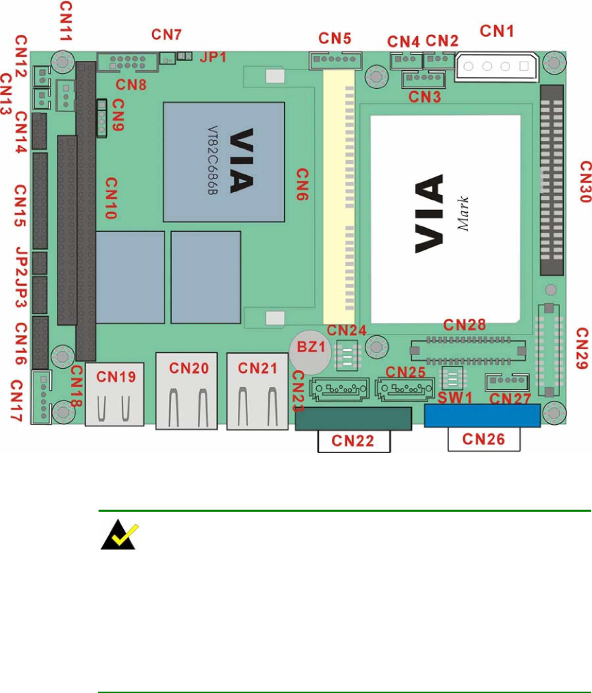
2.2 External Interfaces
For the locations of external interfaces, please refer to the diagram below:
Figure 2-2 External Interfaces
NOTE:
1. The configuration options through jumper settings will be discussed
in Chapter 3: Installation.
2. On the solder side, there are a CFII card socket and a FDC floppy
connector.
2-8
3301770
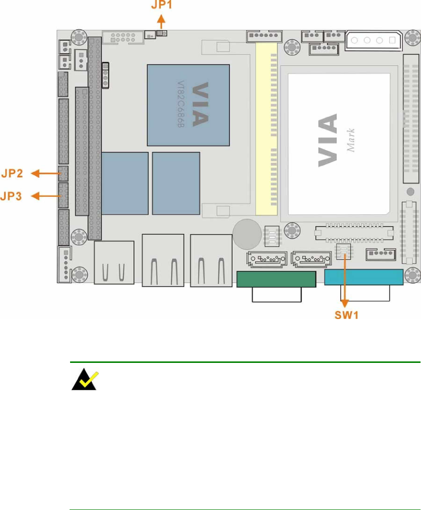
Shown below is a diagram indicating the locations of configuration jumpers.
Figure 2-3 Locations of Configuration Jumpers
NOTE:
1. Only configuration jumpers are shown in the diagram above.
2. The SW1 DIP switch is left unused, and the associated LVDS mode
configuration can be found in BIOS setting.
3. For more configuration details on jumper settings, please refer to
Chapter 3 Installation.
2-9

3301770
Table 2-3 Interface Connectors
Function
CN1 4P power connector
CN2 3-pin PS-ON/ATX feature connector
CN3 5-pin Inverter control
CN4 3-pin CPU fan connector
CN5 5-pin External LED connector (to chassis LED control PCB)
CN6 144-pin SDRAM SO-DIMM socket
CN7 2-pin connector to the external Lithium 3V coin cell battery-
CN8 10-pin audio connector (to the external adapter cable kit which
should provide phone jacks for Line_out, Line_in, and MIC_in
connectivity)
CN9 4-pin Audio CD_IN connector
CN10 PC/104 connector (104-pin ISA bus)
CN11 3-pin external -VCC power connector
.
It is a peripheral power
connector, provides a -5V and -12V sources as -VCC voltage that
are supplementary to the PC104 (CN10) connector.
CN12 2-pin Reset button switch (to the chassis front panel)
CN13 2-pin Power switch button (to the chassis front panel)
CN14 10-pin general purpose I/Os connector
CN15 26-pin parallel port pin header
CN16 14-pin 2.0mm internal serial port pin header (COM2)
CN17 6-pin keyboard/mouse connector (a 6-pin-to-PS/2 adapter cable is
required)
CN18 Not implemented
CN19 External USB1.1 connector (2 ports)
CN20 10/100BaseT Ethernet port
CN21 10/100BaseT Ethernet port
CN22 External D-SUB 9 serial port connector (COM1)
CN23 Serial ATA connector
CN24 8-pin internal 2.0mm USB header (an adapter cable required)
CN25 Serial ATA connector
2-10

3301770
CN26 D-SUB 15-pin VGA connector
CN27 5-pin 2.54mm IrDA connector
CN28 TFT LCD connector (DF13-40P-1.25V)
CN29 LCD panel dual-channel 18-bit LVDS/TTL connector, 30 (2x15) pin
header 1.25mm (DF13-30P-1.25V)
CN30 Primary IDE bus connector (44-pin 2.0mm)
CN31 FPC flat type floppy port (one floppy drive only)
CN32 Compact flash storage card socket (behaves as an IDE device
through BIOS setting)
2.2.1 Internal Connectors
1. CN1: Power 4P Connector
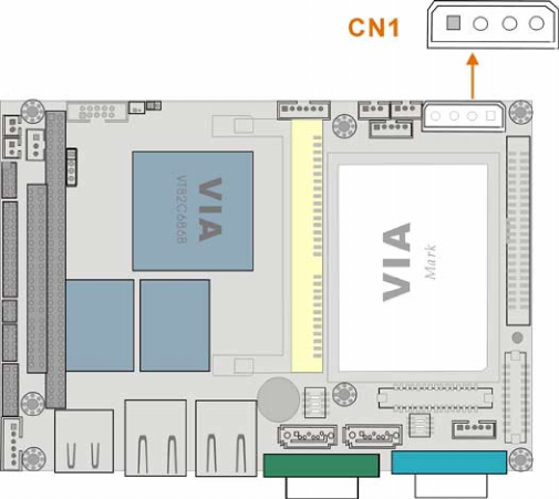
The 3301770-R10 is equipped with an onboard external power connector, CN1. You can
connect power directly to CN1 or mount a PC104 compact-size power supply module on top
of the board through the PC-104 interface.
Table 2-4 CN1: Power 4P Connector
PIN DESCRIPTION
1 +5V
2 GND
3 GND
4 +12V
2-11
3301770
Figure 2-4 Power 4P Connector
2. CN2: SBVCC ATX Power Feature Connector
1x3 2mm connector
Using CN2 as a Power Feature Connector:
The SBVCC connector can support an advanced soft power switch function. If an
ATX power supply is used, connect an ATX-to-4P power cable between the SBVCC connector
and ATX power source. Also connect a power on/off switch to the ATX ON/OFF switch
previously mentioned. Note that your ATX power supply should provide a 10mA load on the
5V source standby lead for this function to take effect.
Provides is an ATX-to-4P adapter cable that comes with a 20-pin ATX connector, a 3-pin
connector to the SBVCC connector, and a 4P power connector.
Using CN2 as a Configuration Jumper:
A jumper cap is installed on pins 1 and 2 as factory default (pin1=+5VSB; pin2=+5V). If the
3301770 is connected to an AT power, let the jumper stay on pins 1 and 2. If connected to an
ATX power source, remove the jumper cap.
2-12
3301770
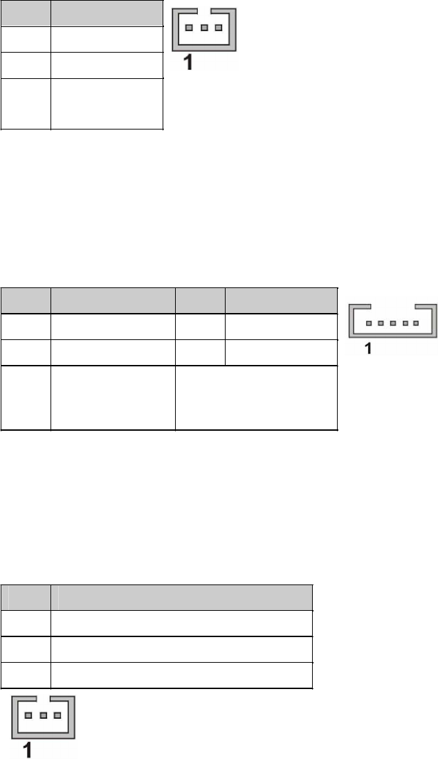
Table 2-5 CN2 SBVCC: ATX Power Feature Pinouts
PIN DESCRIPTION
1 5VSB
2+5V
3 GND Figure 2-5 SBVCC ATX Power Feature
3. CN3: IVTC LCD Panel Inverter Backlight Control Connector
This connector comes as a 1x5 pin 2mm connector.
Table 2-6 CN3 IVTC Inverter Control Pinouts
PIN DESCRIPTION PIN DESCRIPTION
1 VCC12 2 GROUND
3 VEEON 4 BLADJ
5VCC5 Figure 2-6
Inverter Backlight Control
4. CN4: CPU Fan Connector
FAN1 provides access to a +5V power source and a sensor pin for connecting a cooling fan.
Table 2-7 CN4 Fan Connector
PIN DESCRIPTION
1Fan Speed Detect
2+5V
3 GND
Figure 2-7 CN4 Fan Connector
2-13
3301770
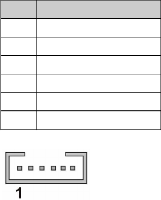
5. CN5: Power and HDD LED Connector
This port provides the connectivity to the power and hard drive activity LEDs on the chassis
front panel. An adapter cable is required.
Table 2-8 CN5 Pinouts
PIN DESCRIPTION
1VCC5
2GROUND
3POWER LED+
4 POWER LED-(GND)
5HDD LED+
6HDD LED-
Figure 2-8 CN5 Power and HDD LED Connector
6. CN6: SDRAM 144-pin SODIMM Socket
This socket receives 100/133MHz SODIMM modules
7. CN7: Battery Connector
This 2-pin header connects to an externally mounted 3V, Lithium, cell coin battery (VARTA
CR2032). The life expectancy of the battery is approximately 7 years. Depending on the
working condition, the life expectancy may be shorter.
Replacing a battery is not a user operation.
If the battery starts to weaken and loses voltage, contact your vendor for a replacement
module. Dispose of the used battery properly. You may contact your local waste disposal
agency for disposal instructions. Do not dispose of a used battery with normal household
2-14
3301770
waste.
WARNING!
1. Keep a used battery away from children.
2. Danger of explosion if the battery is incorrectly replaced. Only
certified module from GAI can be used as a replacement.
3. Do not expose the battery to excessive heat or fire.
4. If the battery shows signs of leakage, contact your local vendor
immediately.
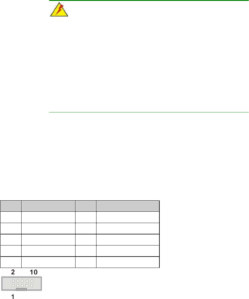
8. CN8: 2x5 2.0mm Audio Pin Header
This port connects to AC’97 compatible audio devices through an adapter cable, e.g., that
features a 10-pin header to audio phone jacks on a slot bracket.
Table 2-9 CN8 Audio Pinouts
PIN DESCRIPTION PIN DESCRIPTION
1 LINE OUT R 2 LINE IN R
3 GROUND 4 GROUND
5 LINE OUT L 6 LINE IN L
7 GROUND 8 GROUND
9 MIC IN 10 N/C
Figure 2-9 CN8 Audio Port
2-15
3301770
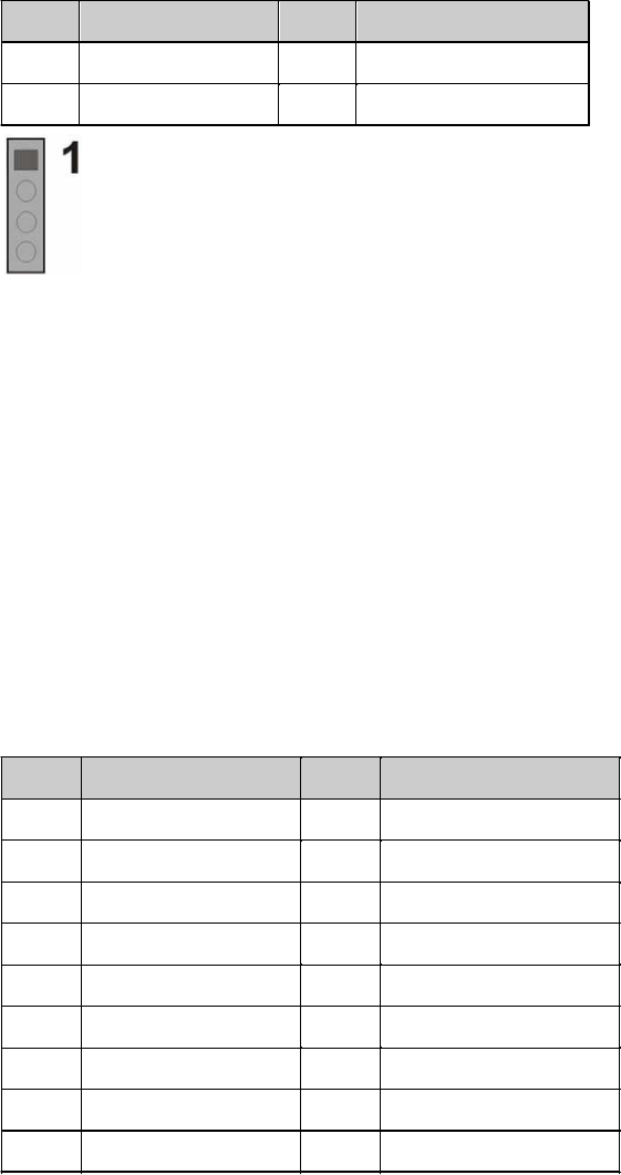
9. CN9: Audio CD_IN Header
This 4-pin header connects to audio source such as CD/DVD-ROM optical drives.
Table 2-10 CN9 Audio CD_IN Pinouts
PIN DESCRIPTION PIN DESCRIPTION
1 LINE_IN L 2 GND
3 GND 4 LINE IN R
Figure 2-10 CN9 Audio CD_IN Port
10. CN10: PC-104 (104-pin ISA bus) Connector
The 3301770 features a PC/104 expansion bus that let you attach any kind of PC-104
modules. The PC-104 bus has already become the industrial embedded PC bus standard, so
you can easily install over thousands of PC-104 modules from hundreds of vendors in the
world. There are two PC-104 connectors on this board: PC/104-64 and PC/104-40.
A -5V/-12V (-VCC) connector is provided to supply -VCC voltage that is routed through the PC
104 64-pin connector.
Table 2-11 PC/104-64 Connector Pinouts
PIN DESCRIPTION PIN DESCRIPTION
1 IOCHECK# 33 GROUND
2 SD7 34 IRSTDRV
3 SD6 35 VCC
4 SD5 36 IRQ9
5 SD4 37 -5V
6 SD3 38 DRQ2
7 SD2 39 -12V
8 SD1 40 ZWS
9 SD0 41 +12V
2-16

3301770
10 IOCHRDY 42 GROUND
11 AEN 43 SMEMW#
12 LA19 44 SMEMR#
13 LA18 45 IOW#
14 LA17 46 IOR#
15 SA16 47 DACK3#
16 SA15 48 DRQ3
17 SA14 49 DACK1#
18 SA13 50 DRQ1
19 SA12 51 REFRESH#
20 SA11 52 SYSCLK
21 SA10 53 IRQ7
22 SA9 54 N/C
23 SA8 55 IRQ5
24 SA7 56 IRQ4
25 SA6 57 IRQ3
26 SA5 58 DACK2
27 SA4 59 TC
28 SA3 60 BALE
29 SA2 61 VCC
30 SA1 62 OSC
31 SA0 63 GROUND
32 GROUND 64 GROUND
Table 2-12 PC/104-40 Connector Pinouts
PIN DESCRIPTION PIN DESCRIPTION
1 GROUND 21 GROUND
2 MCS16# 22 SBHE#
3 IOCS16# 23 LA23
4 IRQ10 24 LA22
5 IRQ11 25 LA21
6 IRQ12 26 LA20
7 IRQ15 27 LA19
2-17

3301770
8 IRQ14 28 LA18
9 DACK0# 29 LA17
10 DRQ0 30 MEMR#
11 DACK5# 31 MEMW#
12 DRQ5 32 SD8
13 DACK6# 33 SD9
14 DRQ6 34 SD10
15 DACK7# 35 SD11
16 DRQ7 36 SD12
17 VCC 37 SD13
18 MASTER# 38 SD14
19 GROUND 39 SD15
20 GROUND 40 GROUND
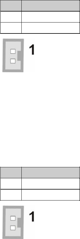
11. CN11: External –VCC Power Connector
Table 2-13 CN11 -VCC PC/104 Supplementary Power
PIN DESCRIPTION
1 -5V
2 GND
3 -12V
Figure 2-11 CN11 –VCC Power
2-18
3301770
12. CN12: Reset Button Connector
This connector connects to an externally implemented reset button through an adapter cable.
Table 2-14 CN12 Reset Button Connector Pinouts
PIN DESCRIPTION
1 RST_SW
2 GND
Figure 2-12 CN12 Reset Button Connector
13. CN13: Power ON/OFF Button Connector
This connector connects to an externally implemented ON/OFF button through an adapter
cable.
Table 2-15 CN13 Power ON/OFF Button Connector Pinouts
PIN DESCRIPTION
1 RST_SW
2 GND
Figure 2-13 CN13 Power ON/OFF Button Connector
2-19
3301770
14. CN14: Digital I/O Connector
This Digital I/O port is managed through VIA’s VT82C686B Southbridge. The first table
below shows the CN14 port pinouts. The second table displays the referential pin connection
to the I/O chip.
Table 2-16 CN14 Digital I/O Connector Pinouts
PIN DESCRIPTION PIN DESCRIPTION
1 GND 2 +5V
3 DIO_IN0 4 DIO_OUT0
5 DIO_IIN1 6 DIO_OUT1
7 DIO_IN2 8 DIO_OUT2
9 DIO_IN3 10 DIO_OUT3
Table 2-17 Digital I/Os to Southbridge Reference Chart
PIN CN14 PINS SOUTHBRIDGE
PINS DESCRIPTION
1 GND - -
3 DIO_IN0 SDD6/JBY -
5 DIO_IIN1 SDD7/JBX -
7 DIO_IN2 BATLOW/GPI2 Connect to 10K-ohm pull-up to +3.3V
suspend power if the function is not applied.
9 DIO_IN3 SM BALT/GPI6
„
Connect to 10K-ohm pull-up to +3.3V
suspend power if the function is not
applied.
„
Connect to 4.7K-ohm pull-up to +3.3V.
PIN CN14 PINS SOUTHBRIDGE
PINS DESCRIPTION
2 +5V - -
4 DIO_OUT0 GPIOA/GPIO8 Connect to 2.2K-ohm series resistor.
6 DIO_OUT1 Fan2/GPIOB/GP
10
Connect to 10K-ohm pull-up to +3.3VBAT
power if no multiplexed function is applied.
2-20
3301770
8 DIO_OUT2 MCCS/GPIOD Connect to 10K-ohm pull-up to +3.3VBAT
power if no multiplexed function is applied.
10 DIO_OUT3 PCI STP/GPO5 Connect to 4.7K-ohm pull-up to +3.3V power
if the function is not applied.
Figure 2-14 CN14 Digital I/O Connector
15. CN15: Parallel Port Connector
2x13 pin header 2mm connector
CN15 is an IEEE1284 compatible interface. Usually, the parallel port connects to a printer.
This port is provided as a 26-pin 2.0mm pin header.
An adapter cable is required, (2x13 pin header-to-parallel D-SUB w/
screws for securing to a chassis panel)
Table 2-18 CN15 Parallel Port Pinouts
PIN DESCRIPTION PIN DESCRIPTION
1STROBE# 14 AUTO FORM FEED#
2DATA0 15 ERROR#
3DATA1 16 INITIALIZE
4DATA2 17 PRINTER SELECT LN#
5DATA3 18 GROUND
6DATA4 19 GROUND
7DATA5 20 GROUND
8DATA6 21 GROUND
9DATA7 22 GROUND
10 ACK- 23 GROUND
11 BUSY 24 GROUND
2-21
3301770
12 PAPER EMPTY 25 GROUND
13 PRINTER SELECT 26 N/C
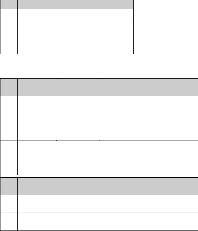
Figure 2-15 CN15 Parallel Port
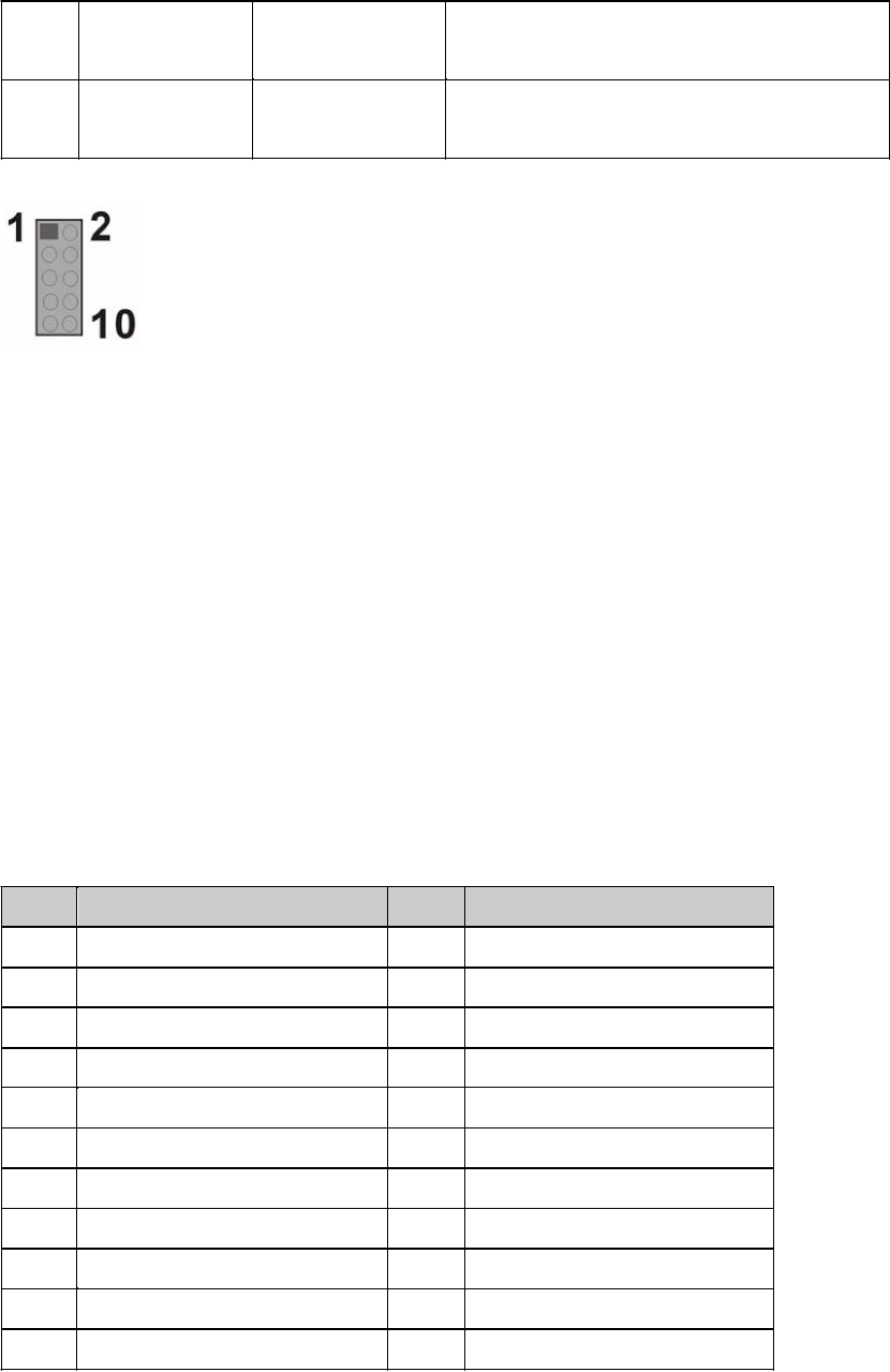
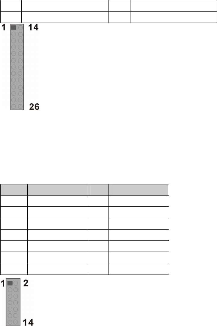
16. CN16: COM2 RS-232/422/485 Serial Port Header
Table 2-19 COM2: 14 (2x7) Pin 2.0mm Connector Pinouts
PIN DESCRIPTION PIN DESCRIPTION
1 NRLSD2 2 NDSR2
3 NRX2 4 NRTS2
5 NTX2 6 NCTS2
7 NDTR2 8 COM_R12
9 GND 10 GND
11 TX2+ 12 TX2-
13 RX2+ 14 RX2-
Figure 2-16 COM2 Connector
2-22
3301770
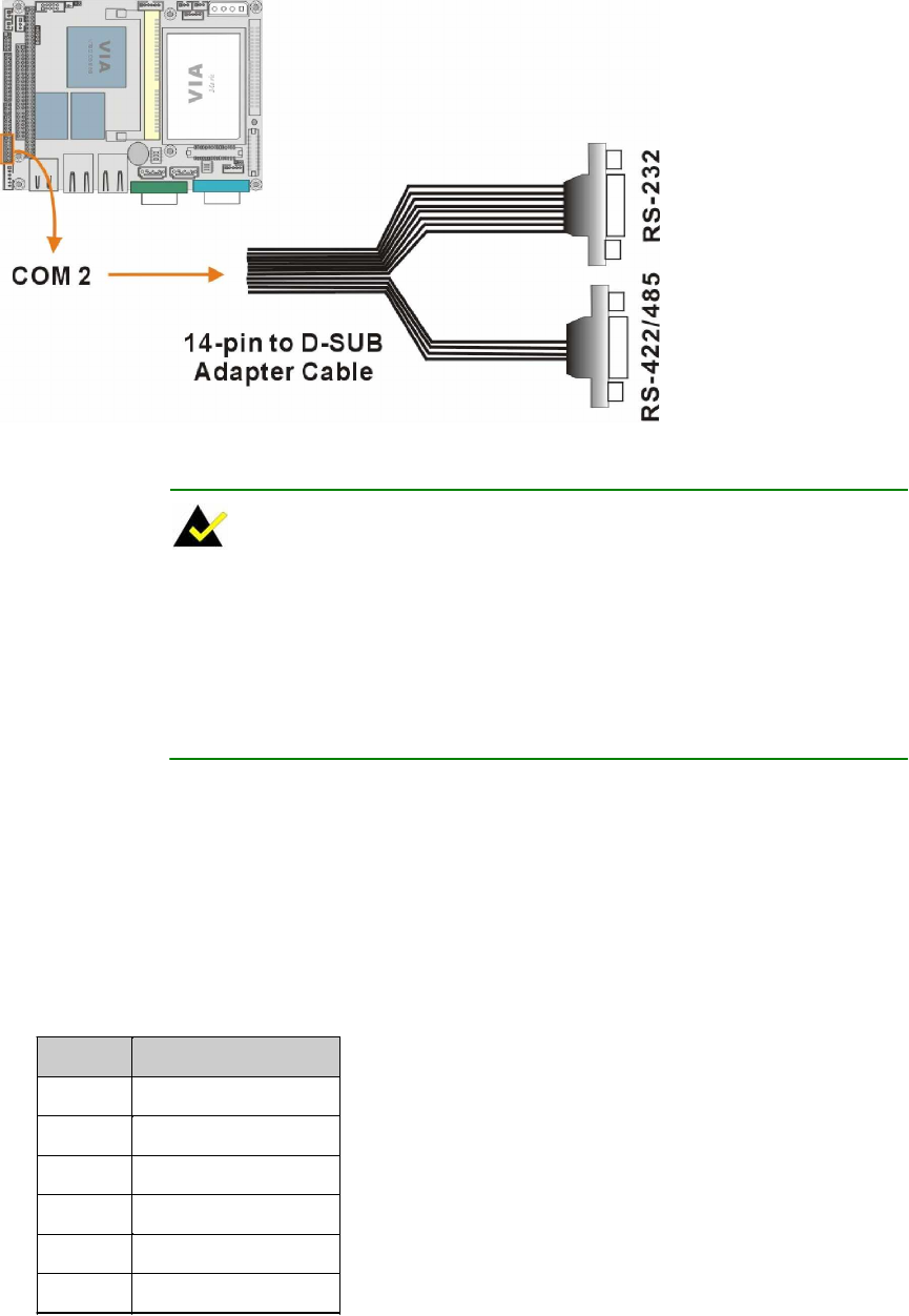
Figure 2-17 COM2 Adapter Cable
NOTE:
1. If you want to use the RS485 mode, just connect to TX2-, TX2+. If
you want to use the RS422, please connect to TX2-, TX2+, RX2+,
and RX2-.
2. Please refer to Chapter 3 for details on serial port operation modes.
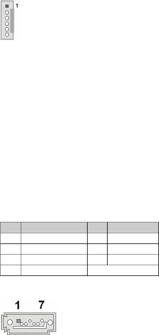
17. CN17: Keyboard/Mouse Pin Header
This port connects to a PS/2 keyboard or mouse using a 6-pin-to-PS/2 adapter cable. An
adapter cable, 6-pin-to-two PS/2, is required.
Table 2-20 CN17 Keyboard/Mouse Header Pinouts
PIN DESCRIPTION
1 +5V
2 MS_DATA
3 MS_CLK
4 KB_DATA
5 KB_CLK
6 GND
2-23
3301770
Figure 2-18 CN17 Keyboard/Mouse Pin Header
18. CN18:
Factory reserved.
19. CN19, CN20, CN21, CN22, and CN26: Front Panel Connectors
These are front panel connectors. Please refer to the next section for details.
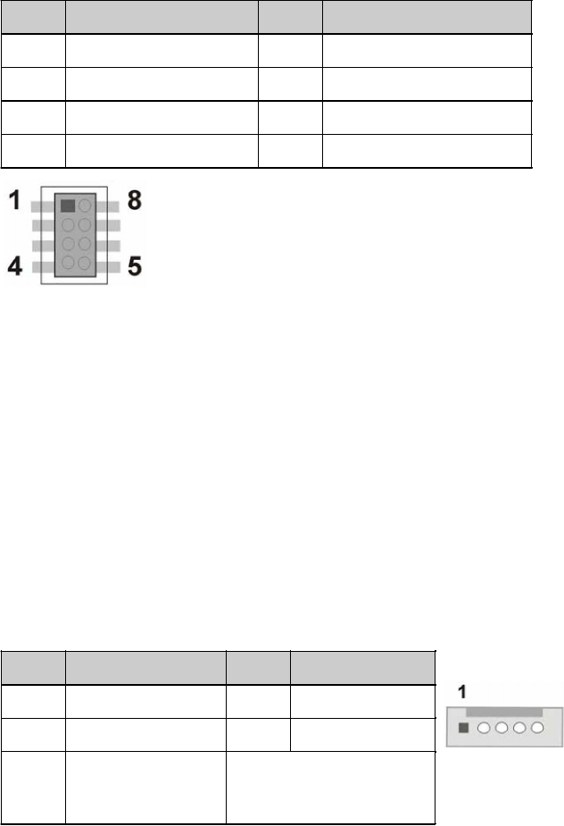
20. CN23 & CN25: Serial ATA Disk Drive Connectors
These 7-pin standard Serial ATA ports connect to SATA I-compatible hard disk drives. SATA
drives are managed by the ALi chipset onboard.
Table 2-21 Serial ATA Port Pinouts
PIN DESCRIPTION PIN DESCRIPTION
1 GND 2 STXP
3STXN 4 GND
5SRXN 6SRXP
7 GND
Figure 2-19 Serial ATA Port
2-24
3301770
21. CN24: Internal USB Header (Two Ports)
USB0/1: 2x4 8-pin Header
This header provides the connectivity to additional USB devices through an adapter cable.
Various adapters may come with USB ports on a slot bracket or ports that can be attached to
D-SUB openings on a chassis.
Table 2-22 CN24 USB Port Pinouts
PIN DESCRIPTION PIN DESCRIPTION
1+5V 8 GND
2USBDT2N 7USBDT3P
3USBDT2P 6USBDT3N
4 GND 5 +5V
Figure 2-20 CN24 USB (1.1) Port
22. CN27: IrDA Port
This pin header allows you to connect external Infrared devices through an adapter cable.
The IrDA port supports either a Serial Infrared (SIR) or an Amplitude Shift Keyed IR(ASKIR)
interface. The header comes as a 1x5 pin 2.54mm pin header.
Table 2-23 CN27 IrDA Interface Port Pinouts
PIN DESCRIPTION PIN DESCRIPTION
1+5V 2 N/C
3IR-RX 4 GROUND
5IR-TX Figure 2-21
CN27 IrDA Interface Port
2-25

3301770
23. CN28: Flat Panel Display Connector
TFT LCD (24-bit one channel; DF13-40DP-1.25V )
Table 2-24 CN28 Flat Panel Connector Pinouts
PIN DESCRIPTION PIN DESCRIPTION
2LCD5V 1LCD5V
4 GROUND 3 GROUND
6LCD3V 5LCD3V
8 GROUND 7 N/C
10 FPD1 9 FPD0
12 FPD3 11 FPD2
14 FPD5 13 FPD4
16 FPD7 15 FPD6
18 FPD9 17 FPD8
20 FPD11 19 FPD10
22 FPD13 21 FPD12
24 FPD15 23 FPD14
26 FPD17 25 FPD16
28 FPD19 27 FPD18
30 FPD21 29 FPD20
32 FPD23 31 FPD22
34 GROUND 33 GROUND
36 FPVS 35 FPCLK
38 FPHS 37 FPDEN
40 ENVEE 39 N/C
Figure 2-22 CN28 TFT Panel Display Connector
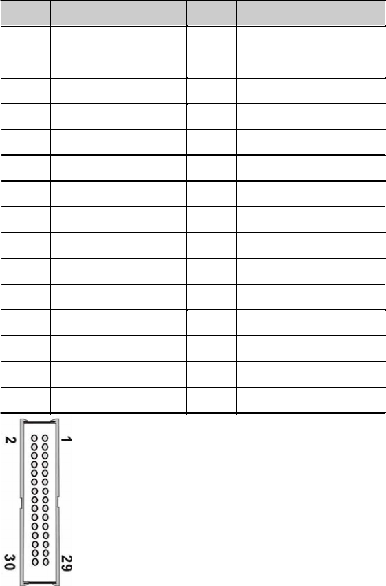
24. CN29: LVDS Panel Display Connector
LVDS LCD (18-bit) 2x15 pin header 1.25mm (DF13-30DP-1.25V)
2-26
3301770
Table 2-25 CN29 LVDS Connector Pinouts
PIN DESCRIPTION PIN DESCRIPTION
2 GND 1 GND
4 LVDSA_Y0- 3 LVDSA_Y0+
6 LVDSA_Y1- 5 LVDSA_Y1+
8 LVDSA_Y2- 7 LVDSA_Y2+
10 LVDSA_CLK- 9 LVDSA_CLK+
12 N/C 11 N/C
14 GROUND 13 GROUND
16 LVDSB_Y0- 15 LVDSB_Y0+
18 LVDSB_Y1- 17 LVDSB_Y1+
20 LVDSB_Y2- 19 LVDSB_Y2+
22 LVDSB_CLK- 21 LVDSB_CLK+
24 N/C 23 N/C
26 GROUND 25 GROUND
28 VCC5_LVDS 27 VCC5_LVDS
30 VCC3_LVDS 29 VCC3_LVDS
Figure 2-23 CN29 LVDS Panel Display Connector
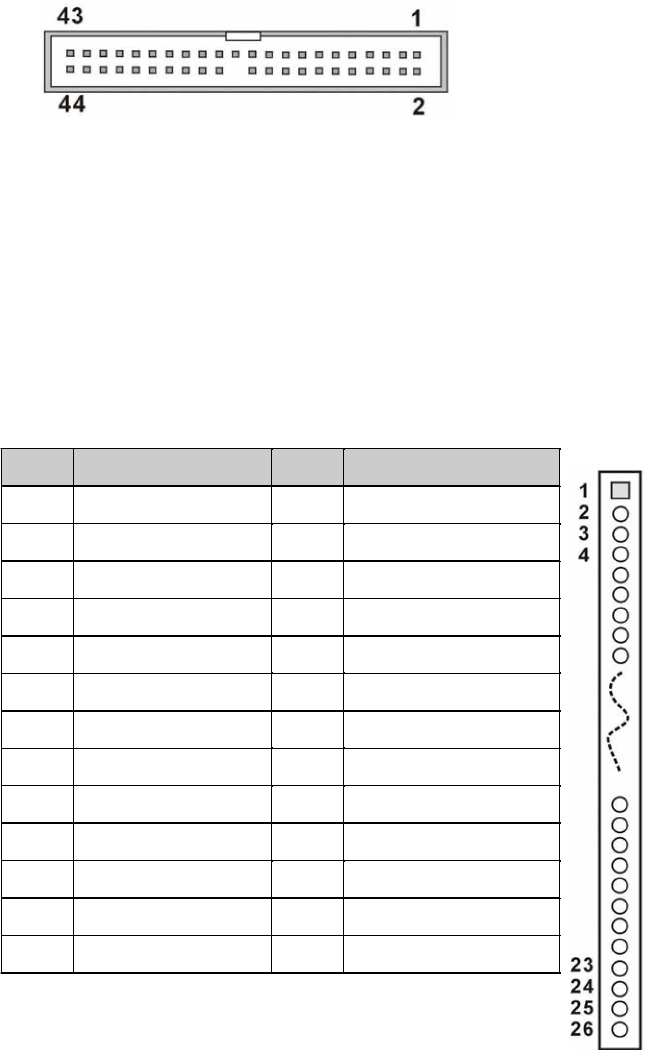
25. CN30: IDE Connector
One IDE connector can connect to one (1) IDE cable, and the single IDE cable can then
connect to two IDE devices. An optional IDE adapter cable is available.
2-27

3301770
Table 2-26 CN30 IDE Connector Pinouts
PIN DESCRIPTION PIN DESCRIPTION
1 RESET# 2 GROUND
3 DATA 7 4DATA 8
5 DATA 6 6DATA 9
7 DATA 5 8DATA 10
9 DATA 4 10 DATA 11
11 DATA 3 12 DATA 12
13 DATA 2 14 DATA 13
15 DATA 1 16 DATA 14
17 DATA 0 18 DATA 15
19 SIGNAL GND 20 (KEY)
21 HDD 0 22 GROUND
23 IO WRITE 24 GROUND
25 IO READ 26 GROUND
27 HD READY 28 N/C
29 HDACK 0 30 GROUND
31 IRQ14 32 N/C
33 ADDR 1 34 N/C
35 ADDR 0 36 ADDR 2
37 HDD SELECT 0 38 HDD SELECT 1
39 IDE ACTIVE# 40 GROUND
41 VCC 42 VCC
43 GROUND 44 N/C
2-28
3301770
Figure 2-24 IDE Connector
26. CN31: Optional Floppy Connector (On the Soldering Side)
A 26-pin FPC connector cable is required for connecting to the optional floppy port. You can
connect one (1) 3.5”(720 KB, 1.44 MB, and 2.88 MB) drive to this port.
Table 2-27 CN31: Optional Floppy Connector
PIN DESCRIPTION PIN DESCRIPTION
1 VCC 14 STEP#
2 INDEX# 15 GROUND
3 VCC 16 WDATA#
4 DISKSEL0# 17 GROUND
5 VCC 18 WGATE#
6 DSKCHG# 19 GROUND
7 N/C 20 TRAK0#
8 N/C 21 GROUND
9 N/C 22 WRTPRT#
10 MTR0# 23 GROUND
11 N/C 24 RDATA#
12 DIR# 25 GROUND
13 N/C 26 HDSEL#
Figure 2-25
CN31 Floppy Port
2-29

3301770
27. CN32: Compact Flash Connector)
The CN32 socket allows you to attach a Compact Flash Disk that occupies the secondary IDE
channel. The CN32 socket supports both the TYPE II and TYPE I modules.
Table 2-28 CN32 Pinouts
PIN DESCRIPTION PIN DESCRIPTION
1 GROUND 26 VCC-IN CHECK1
2 DATA3 27 DATA11
3 DATA4 28 DATA12
4 DATA5 29 DATA13
5 DATA6 30 DATA14
6 DATA7 31 DATA15
7 HDC_CS0# 32 HDC_CS1
8 N/C 33 N/C
9 GROUND 34 IOR#
10 N/C 35 IOW#
11 N/C 36 VCC_COM
12 N/C 37 IRQ15
13 VCC_COM 38 VCC_COM
14 N/C 39 CSEL
15 N/C 40 N/C
16 N/C 41 HDD_RESET
17 N/C 42 IORDY
18 SA2 43 SDREQ
19 SA1 44 SDACK#
20 SA0 45 HDD_ACTIVE#
21 DATA0 46 PDIAG
22 DATA1 47 DATA8
23 DATA2 48 DATA9
24 N/C 49 DATA10
25 VCC-IN CHECK2 50 GROUND
2-30
3301770
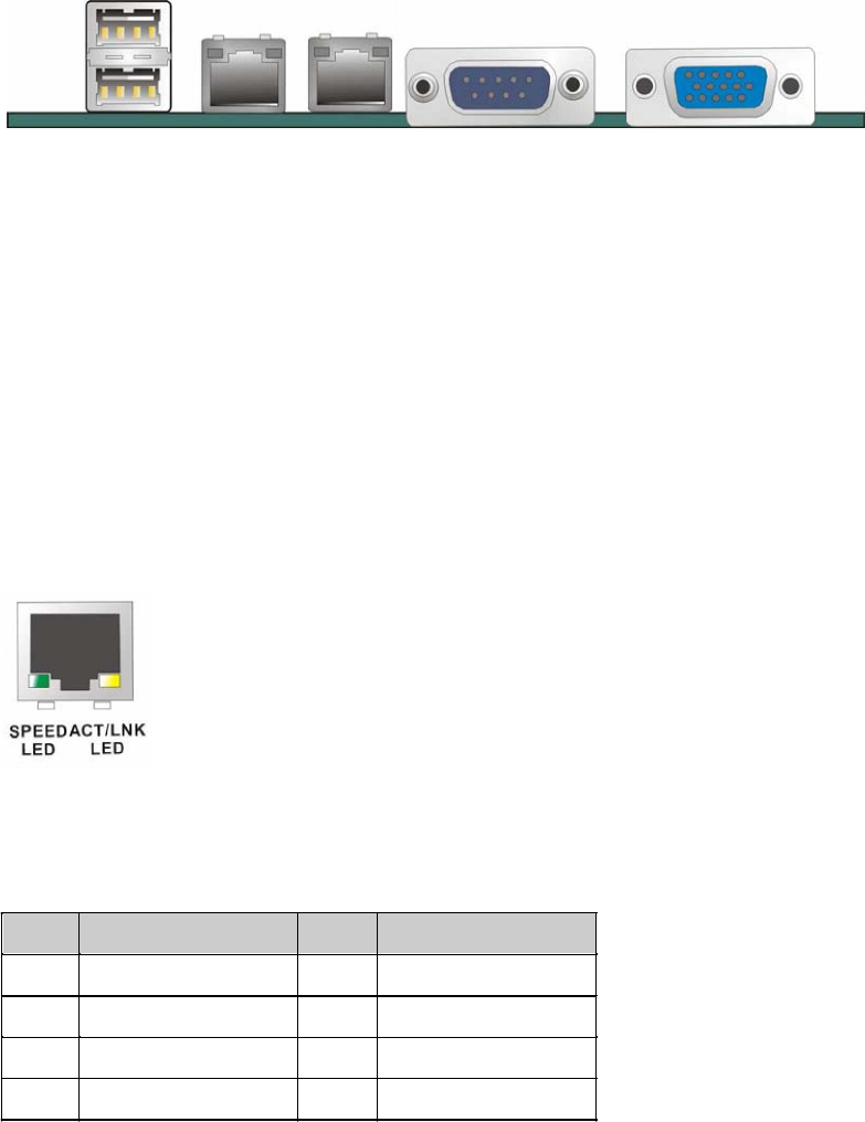
2.2.2 Front Panel Connectors
Figure 2-26 Front Panel Connectors
CN19: USB Combo Connector (2 Ports)
The combo connector provides two USB ports. These two USB ports connect to USB1.1
devices.
CN20 & CN21: 10/100BaseT Ethernet (RJ-45) Ports
These RJ-45 connectors provide 10/100BaseT Ethernet connection to a local or internet
network. Refer to the table below for the Ethernet port LED indication.
Figure 2-27 10/100BaseT Ethernet (RJ-45) Port
Table 2-29 Ethernet Port Pinouts
PIN DESCRIPTION PIN DESCRIPTION
1TX- 5 N/C
2 N/C 6 RX-
3TX- 7 N/C
4RX+ 8 N/C
2-31

3301770
Ethernet Port LED Indicators
Table 2-30 Ethernet Port LED Indications
ACTIVITY LED LINK LED
Status Description Status Description
GREEN Activity YELLOW Linked
CN22: Serial Port COM1
This serial port is defined as COM1 and provides serial connection in the RS-232 mode.
Table 2-31 Serial Port COM1 Pinouts
PIN DESCRIPTION PIN DESCRIPTION
1 NRLSD1 6NDSR1
2NRX1 7NRTS1
3NTX1 8NCTS1
4NDTR1 9 COM_RI1
5 GND
CN26: VGA Port
This 15-pin D-SUB VGA port connects to a CRT or LCD display monitor.
Table 2-32 VGA Port Pinouts
PIN DESCRIPTION PIN DESCRIPTION
1VGA_R 9 N/C
2VGA_G 10 GND
3VGA_B 11 N/C
4 N/C 12 SSDA
5 GND 13 VGA_HS
6 GND 14 VGA_VS
7 GND 15 SSCL
8 GND
2-32

3301770
Chapter
3
Installation
3-1
3301770
3.1 Considerations Prior to Installation
Preparing Your Embedded Board
The embedded board contains numerous delicate electronic circuits and components, which can
become damaged as a result of electrostatic discharge (ESD). Thus, prior to installation, please
follow the instructions below:
1. Please turn off the computer and unplug its power cord.
2. When handling the board, avoid touching any metal leads or connectors.
3. It is best to wear an electrostatic discharge (ESD) cuff when handling electronic components
(CPU, RAM).
4. Prior to installing the electronic components, please have these items on top of an antistatic
pad or within an electrostatic shielding container.
5. Please verify that the power supply is switched off before unplugging the power supply
connector from the motherboard.
Installation Notices
1. Prior to installation, please do not remove the stickers on the system board. These stickers are
required for warranty validation.
2. Prior to the installation of the system board or any hardware, please first carefully read the
information in the provided manual.
3. Before using the product, please verify that all cables and power connectors are connected.
4. To prevent damage to the PCB board, please do not allow screws to come in contact with the
PCB circuit, connector pins, or its components.
5. Please make sure there are no leftover screws or metal components placed on the PCB board
or within the computer casing.
6. Please do not place the computer system on an uneven surface.
7. Turning on the computer power during the installation process can lead to damage to system
components as well as physical harm to the user.
8. If you are uncertain about any installation steps or have a problem related to the use of the
product, please consult a certified computer technician.
3-2
3301770
Airflow Consideration
Although the embedded board can operate without active cooling, it is still necessary to install the
board in a chassis with ventilation holes on the sides allowing airflow to travel through the heatsink
surface. In a system with an individual power supply unit, the cooling fan of a power supply can
also help generate airflow through the board surface.
Unpacking Precautions
Some components on the 3301770 are very sensitive to static electric charges and can be
damaged by a sudden rush of power. To protect it from unintended damage, be sure to follow
these precautions:
z
Ground yourself to remove any static charge before touching your PCB. You can do
so by using a grounded wrist strap at all times or by frequently touching any
conducting materials that is connected to the ground.
z
Handle your PCB by its edges. Do not touch IC chips, leads or circuitry if not
necessary.
z
Do not plug or unplug any connector or jumper while the power is on.
z
Do not place a PCB on top of an anti-static bag. Only the inside of the bag is safe
from static discharge.
Approved Memory Modules
(144pin SODIMM modules)
1). 128MB SDRAM (PC-100) UG NEC (D45128163G5-A80-9JF)
2). 256MB SDRAM (PC-100) Transcend SAMSUNG (K4S280832A-TC1H)
3). 64MB SDRAM (PC-133) UG HYUNDAI (HY57V651620B)
4). 128MB SDRAM (PC-133) NEC (D45128841G5-A75-9JF)
5). 256MB SDRAM (PC-133) UG SAMSUNG (K4S560832B-TC75))
6). 512MB SDRAM (PC-133) UG (V54C3256804VBSG)
7). 512MB SDRAM (PC-133) Apacer V54C3256804AB7
3-3
3301770
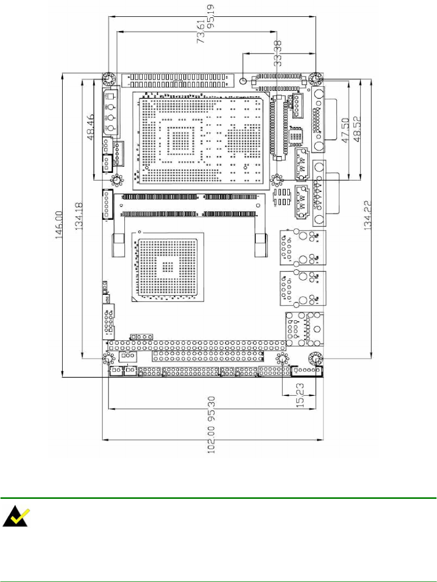
3.2 Mechanical Diagrams
Figure 3-1 Board Dimensions and Mounting Hole Locations
NOTE:
Use the mounting holes on the four corners of the PCB for securing within a chassis.
Holes in the middle of the board are used for securing a heatsink.
3-4
3301770
3.3 Jumper Settings
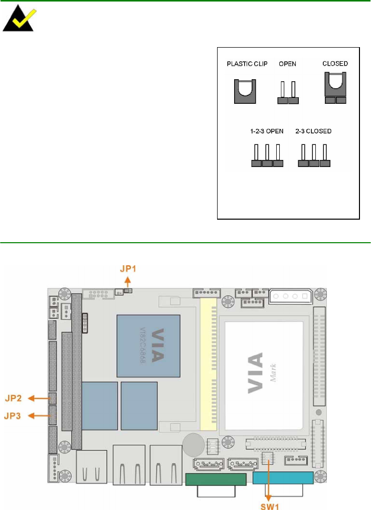
NOTE:
A jumper is a metal bridge that is used to
close an electrical circuit. It consists of
two metal pins and a small metal clip
(often protected by a plastic cover) that
slides over the ins to connect them. To
CLOSE/SHORT a jumper means
connecting the pins of the jumper with the
plastic clip and to OPEN a jumper means
removing the plastic clip from a jumper. Figure 3-2 Jumper
Figure 3-3 Locations of Configuration Jumpers
3-5
3301770
JP1 (Clear CMOS)
In case the embedded board fails to boot due to user’s improper BIOS setting, this jumper can be
used to clear the CMOS data and reset the system BIOS information. To clear the CMOS
contents, shunt pins 2 and 3 for a few seconds, and then reinstall the jumper clip back to pins 1
and 2.
If the “CMOS Settings Wrong” message displays during the boot up process, you may then try to
correct the fault by pressing the F1 to enter the CMOS Setup menu. You may then enter the
correct CMOS setting, Load Optimal Defaults, or Load Failsafe Defaults. Save your changes and
exit the CMOS Setup menu.
JP1 Pin Configuration
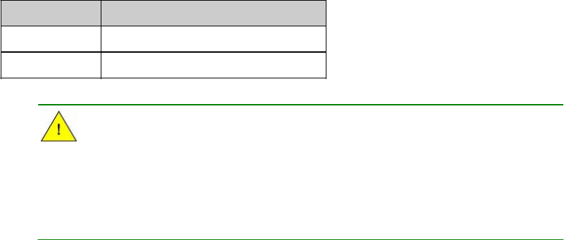
Table 3-1 JP1 Pin Configuration
JP1 CLEAR CMOS
1-2 closed Normal (default)
2-3 closed CLEAR CMOS
CAUTION!
1. In normal condition, pins 1 and 2 must always stay in a CLOSED
condition.
2. Power must be turned OFF before clearing CMOS data.
3-6

3301770
JP2: COM2 Serial Port Operation Mode Selector
This jumper block allows you to select an operation mode for the COM2 serial port (Default:
1-3).
Table 3-2 JP2 Pinouts
PIN
COMBINATION DESCRIPTION
1-2 RS-232
3-4 RS-422
5-6 RS-485
JP3: COM2 Signal Selector
Table 3-3 JP3 COM2 Signal Selector
COM1 Pin-9 Signal Selection COM2 Pin-8 Signal Selection
PIN
COMBINATION DESCRIPTION PIN
COMBINATION DESCRIPTION
1-3 12V 2-4 12V
3-5 5V 4-6 5V
5-7 5V 6-8 5V
7-9 RI1 8-10 RI2
Figure 3-4 JP3 Pin Locations
3-7
3301770
3.4 Installation
Figure 3-5 Soldering Side Sockets
IDE Disk Drive and CDROM Connector
The 3301770 provides 1 IDE channel which allows the connection to two Enhanced Integrated
Device Electronics hard disk drives or CD/DVD-ROM. The IDE controller is attached
to a PCI interface. The advanced IDE controller supports PIO mode 3, mode 4 and up to
UDMA/100 in transfer speed.
Connecting Hard Disk Drives
IDE bus devices are daisy-chained using standard a 144-pin IDE cable. Connection is made by
connecting one end of the cable to the CN30 IDE connector. The connector has a keyed pin which
prevents you from inserting the connector in a wrong direction. The read wire corresponds to pin 1
on the connector.
Plug the other end of the cable into the Enhanced IDE hard drive, with pin 1 on the cable
corresponding to pin 1 on the hard drive.
3-8
3301770
Note that when connecting two IDE disk drives you will have to configure one as the master and
the other the slave. The configuration is done by setting the jumpers on the disk drives.
Optional Floppy Drive Connector (FDD1)
This connector provides access to one (1) externally mounted floppy drive (3.5”-profile, 720 KB,
1.44 MB, and 2.88 MB types floppy drive).
A 26-pin FPC connector cable is required for the connection to floppy drives. The cable should
come with a 26-pin FPC-cable connector and floppy disk drive connector on the other end.
Connecting the Floppy Drive
1. Plug the 26-pin FPC-cable connector into CN31. Make sure that the red wire corresponds to
pin one on the connector.
2. Attach the appropriate connector on the other end of the cable to the floppy drive. You can use
only one connector in the set.
Compact Flash Disk
When appropriately formatted, a compact Flash disk can serve as a bootable hard drive in
applications where installation space is limited. The Compact Flash card occupies a secondary
IDE channel. Configuration options can be found through the BIOS configuration utility.
Parallel Port Connector (CN15)
Parallel port connects to a printer. The 3301770 comes with a multi-mode (ECP/EPP/SPP) parallel
port. The CN15 parallel port interface features a 26-pin flat-cable connector that requires an
adapter cable if a traditional DB-25 connector is preferred. The parallel interface can be
re-assigned to LPT2 or LPT3 through the BIOS configuration utility.
The default interrupt channel is IRQ7. Select ECP or EPP DMA mode using the BIOS
configuration utility.
3-9
3301770
Audio Interface
Audio Connector
AC’97 Audio signals are interfaced through a 10-pin flat-cable connector. These signals include
Microphone line-in, line-in stereo, and line-out stereo. An audio 10-pin-to-phone-jack adapter kit is
required.
COM Port Connectors [COM1(CN22), COM2(CN16)]
The 3301770 provides two serial ports (COM1: RS-232; COM2: RS-232/422/485) interfaced
through one DB-9 connector (COM1) and one 14-pin male header. These serial ports facilitate the
connection to serial devices or a communication network, e.g., terminal console.
LCD Panel Connection (CN26, CN28, and CN29)
The PCI SVGA interface on the 3301770 connects conventional CRT displays and flat panel
displays including passive LCD and active LCD displays. There are three (3) connectors
onboard for the connection to the three (3) display types:
1. CRT VGA monitors
2. TFT flat panel displays
3. LVDS type LCD panels
One CRT display connector (CN26) is provided as a 15-pin, female D-SUB to connect
conventional CRT displays. Pin assignments can be found in Chapter 2 Functional
Description.
Flat Panel Display Connector (CN28):
CN28 is a 40-pin connector, Hirose DF13A-40DP-1.25V, which can support a 24-bit LCD panel.
A bias control signal, ENVEE, active high on CN28, controls the LCD bias voltage. The LCD bias
voltage shall not be applied until the +5V or +3.3V logical supply and panel video signals become
stable. When powered on, the control signal remains low until receiving the flat panel signals.
CN28 connects up to 24-bit TFT LCD.
3-10
3301770
LVDS Connector (CN29):
CN29 is a 20-pin connector, Hirose DF13A-20DP-1.25V. The CN29 connects an 18-bit LCD
panel.
Adapter cables are required for connecting the display connectors.
Ethernet Connection (CN20 & CN21)
The onboard 32-bit PCI-bus Ethernet interface is fully compliant with IEEE 802.3U 10/100Mbps
CSMA/CD standards. The 10/100BaseT connector connections are made via standard RJ-45
connectors on the front edge.
PXE: Pre-Boot Execution Environment
PXE is an open industry standard developed by a number of software and hardware vendors.
BIOS PXE feature allows a workstation to boot from a server on a network by receiving a pre-OS
agent prior to booting the operating system on the local hard drive.
3-11

3301770
Figure
3
-6 PXE Central Management
USB Connection (CN24 and CN19)
The combo USB header (CN24) provides the connectivity of up to two (2) USB (Universal Serial
Bus) ports. The USB interface features complete Plug and Play, and hot attach/detach for up to
127 external devices, compliance with USB specification Rev. 1.1. An adapter 10-pin-to-USB
cable is required for connecting to CN24. The USB interface is accessed through two 5 x 2-pin
connectors, USB01. The adapter cable has one (1) 5x2-pin connector on one end and a
standard USB connector on the other.
3-12

3301770
Accessories Included in Kit
GAI provides the following cables to facilitate connections to your peripheral devices. For more
information on the locations of the connectors, please refer to Chapter 2. Cables not included in kit
are the user supplied items and should be separately purchased.
Table
3
-4 Cables and Accessories Included in Kit
No. Type
1 IDE flat cable 44p/44p
1 COM2 serial port cable (RS-232/422/485 compatible)
1 Audio adapter cable
1 Keyboard/ PS2 mouse Y cable
5 Mini jumper (2.0 pitch)
3-13

3301770
Chapter
4
AMI BIOS Setup
4-1
3301770
Introduction
This chapter discusses AMI's Setup program built into the ROM BIOS. The Setup program allows
users to modify the basic system configuration. This special information is then stored in battery-
backed RAM so that it retains the Setup information when the power is turned off.
Starting Setup
The AMI BIOS is immediately activated when you first power on the computer. The BIOS reads the
system information contained in the CMOS and begins the process of checking out the system
configuration. When it finishes, the BIOS will seek an operating system on one of the disks and
then launch and turn control over to the operating system.
While the BIOS is in control, the Setup program can be activated in one of two ways:
1. By pressing <Del> immediately after switching the system on, or
2. By pressing the <Del> key when the following message appears briefly at the bottom of
the screen during the POST.
Press DEL to enter SETUP.
If the message disappears before you respond and you still wish to enter Setup, restart the system
to try again by turning it OFF then ON or pressing the "RESET" button on the system case. You
may also restart by simultaneously pressing <Ctrl>, <Alt>, and <Delete> keys.
Using Setup
In general, you use the arrow keys to highlight items, press <Enter> to select, use the PageUp and
PageDown keys to change entries, press <F1> for help and press <Esc> to quit. The following
table provides more detail about how to navigate in the Setup program using the keyboard.
Key Function
Up arrow Move to previous item
Down arrow Move to next item
Left arrow Move to the item on the left hand side
Right arrow Move to the item on the right hand side
Esc key Main Menu – Quit and not save changes into CMOS
Status Page Setup Menu and Option Page Setup
Menu -- Exit current page and return to Main Menu
Page Up key Increase the numeric value or make changes
Page Dn key Decrease the numeric value or make changes
F1 key General help, only for Status Page Setup Menu and
Option Page Setup Menu
F2 /F3 key Change color from total 16 colors. F2 to select color
forward.
F10 key Save all the CMOS changes, only for Main Menu
Table 4-1 BIOS Function Keys
4-2

3301770
Getting Help
Press F1 to pop up a small help window that describes the appropriate keys to use and the
possible selections for the highlighted item. To exit the Help Window press <Esc> or the F1 key
again.
If, after making and saving system changes with Setup, you discover that your computer no longer is
able to boot, the AMI BIOS supports an override to the CMOS settings which resets your system to
its defaults.
The best advice is to only alter settings which you thoroughly understand. To this end, we strongly
recommend that you avoid making any changes to the chipset defaults. These defaults have
been carefully chosen by both AMI and your systems manufacturer to provide the absolute
maximum performance and reliability. Even a seemingly small change to the chipset setup has
the potential for causing you to use the override.
NOTE:
Your BIOS setup screen may slightly differ from the screenshots
shown in this chapter. This may result from the modification
changes made during BIOS update.
4-3
3301770
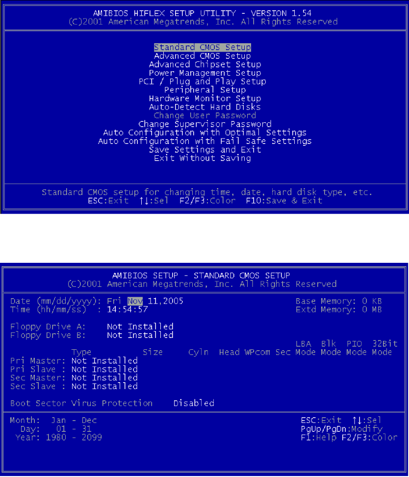
4.1 Setup Summary
„
Standard CMOS Setup:
Standard CMOS Setup: Change time, date, hard disk type, etc.
„
Advanced CMOS Setup:
Advanced CMOS Setup: Configure system options.
„
Advanced Chipset Setup:
Advanced Chipset Setup: Configure chipset features.
„
Power Management Setup:
Power Management Setup: Configure power management features.
„
PCI / Plug and Play Setup:
Configures PCI / Plug and Play features.
„
Peripheral Setup:
Configure peripheral features.
„
Hardware Monitor Setup:
Configure hardware monitor features.
„
Auto-Detect Hard Disks:
Selecting these options allow the user to configure the drive named in the option. Select
Auto-Detect Hard Disks to allow AMIBIOS to automatically configure the drive. A list of drive
parameters appears on the screen.
„
Change User Password:
Change the user password.
„
Change Supervisor Password:
Change the supervisor password.
„
Auto Configuration with Optimal Settings:
Load configuration settings that ensure the highest performance.
„
Auto Configuration with Fail Safe Settings:
Load fails-safe configuration settings.
„
Save Settings and Exit:
Write the current settings to CMOS and exit.
„
Exit Without Saving:
Exit without saving the current settings.
4-4
3301770
4.2 Main Menu Selections
4.3 Standard CMOS Setup Selections
„
Floppy A, B
Move the cursor to these fields and select the floppy type. Available manual setting options
are: [1.2MB 5 1/4] [720KB 3 1/2] [1.44MB 3 1/2] [2.88MB 3 1/2]
„
Primary/Secondary Master/Slave LBA Mode
LBA (Logical Block Addressing) is a new IDE HDD access method to developed to overcome
the 528-megabyte capacity bottleneck. If your IDE hard disk capacity is greater than 528MB,
AMIBIOS can enable this LBA mode feature. The option is only for Primary Master IDE LBA
4-5
3301770
mode.
„
Primary/Secondary Master/Slave Block Mode
If your hard disk drive supports IDE block transfer mode, enable this option for a faster IDE
hard disk drive transfer rate. The option is only for Primary Master Block mode.
„
Primary/Secondary Master/Slave PIO Mode
This option enables Primary Master IDE PIO mode on the IDE, which can set proper cycle
timings. The cycle timing between the IDE PIO mode value and IDE cycle timing is shown
below:
Mode 0 -> Timing (600ns) Mode 1 -> Timing (383ns)
Mode 2 -> Timing (240ns) Mode 3 -> Timing (180ns)
Mode 4 -> Timing (120ns) Mode 5 -> Timing (60ns)
„
Primary/Secondary Master/Slave 32Bit Mode
This option enables Primary Master IDE 32-bit data transfers on the IDE data port. If disabled,
16-bit data transfer is used by the BIOS.32-bit data transfers can only be enabled if IDE
prefetch mode is also enabled.
„
Boot Sector Virus Protection
When this option is enabled, AMIBIOS issues a warning when any program or virus issues a
Disk Format command or attempts to write to the boot sector of the hard disk drive. The
settings are Disabled, Enabled.
4-6
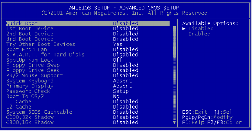
3301770
4.4 Advanced CMOS Setup Selections
„
Quick Boot
The Optimal and Fail-Safe default setting is Disabled. Set this value to Disabled to allow
the BIOS to perform all POST tests. Set this value to Enabled to allow the BIOS to skip
certain POST tests to boot faster.
„
1st Boot Device
This option sets the type of device for the first boot drives that the AMIBIOS attempts to boot
from after AMIBIOS POST completes. The settings are Disabled, IDE-0, IDE-1, Floppy,
ARMD-FDD, ARMD-HDD, CDROM, and SCSI.
„
2nd Boot Device
This option sets the type of device for the second boot drives that the AMIBIOS attempts to
boot from after AMIBIOS POST completes.
The settings are Disabled, IDE-0, IDE-1, Floppy, ARMD-FDD, ARMD-HDD, and CDROM.
„
3rd Boot Device
This option sets the type of device for the third boot drives that the AMIBIOS attempts to boot
from after AMIBIOS POST completes.
The settings are Disabled, IDE-0, IDE-1, Floppy, ARMD-FDD, ARMD-HDD, and CDROM.
„
Floppy Drive Seek
Set this option to Enabled to specify that floppy drives will perform a Seek
operation at system boot. When enabled, the BIOS tests (seeks) floppy drives to
determine whether they have 40 or 80 tracks.
„
Try Other Boot Devices
Set this option to Yes to instruct AMIBIOS to attempt to boot from any other drive in the
4-7
3301770
system if it cannot find a boot drive among the drives specified in the 1st Boot Device, 2nd
Boot Device, 3rd Boot Device, 4th Boot Device options. The settings are Yes or No.
„
Boot from LAN
This option enables you to utilize the PXE LAN control feature.
„
S.M.A.R.T. for Hard Disks
Self-Monitoring, Analysis and Reporting Technology. This option can help the BIOS to warn
the user of a possible device failure and give the user a chance to back up the device before
the failure actually happens.
The settings are Auto, Disabled, Enabled.
„
BootUp Num-Lock
When this option is selected, Num Lock is turned off when the system is powered on so the
user can use the arrow keys on both the numeric keypad and the keyboard.
„
Floppy Drive Swap
This option allows you to swap the A: and B: floppy drive at the BIOS level without physically
change the drives’ connection.
„
Floppy Drive Seek
This option causes the BIOS to search floppy drives at boot time.
„
PS/2 Mouse Support
When this option is enabled, BIOS supports a PS/2- type mouse.
„
System Keyboard
This option does not specify if a keyboard is attached to the computer. Rather, it specifies if
error messages are displayed if a keyboard is not attached. This option permits you to
configure workstation with no keyboard. The settings are Absent, Present.
„
Primary Display
Select this option to configure the type of monitor attached to the computer. The settings are
Monochrome, Color 40x25,Color 80x25,VGA/PGA/EGA, or Not Install.
„
Password Check
To set the system to ask for a password every time it boots.
„
Boot To OS/2
Set this option to Enabled if running OS/2 operating system and using more than 64MB of
system memory on the motherboard. The settings are Disabled or Enabled.
„
L1 Cache
This option can be used to enable or disable the CPU’s L1 cache. The default is Enabled.
4-8
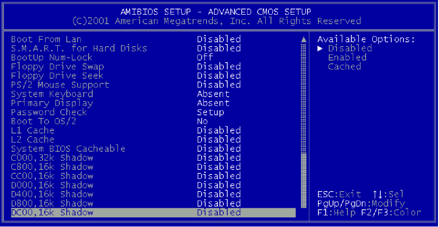
3301770
„
L2 Cache
This option can be used to enable or disable the CPU’s L2 cache. The default is Enabled.
„
System BIOS Cacheable
When this option is set to enable, the System ROM area from F0000-FFFFF is copied
(shadowed) to the RAM for faster execution.
Shadowing the BIOS code from ROM to the much faster system RAM increases
performance. Enabling this setting will also allow the system to cache the RAID where
BIOS resides, and hence more performance is gained.
„
00,32k Shadow
When this option is set to enable, the Video ROM area from C0000-C7FFF is copied
(shadowed) to the RAM for faster execution.
Disabled: The contents of the video ROM are not copied to the RAM.
Cached: The contents of the video ROM area from C0000h - C7FFFh are copied from
the ROM to the RAM and can be written to or read from the cache memory.
Enabled: The contents of the video ROM area from C0000h - C7FFFh are copied
(shadowed) from the ROM to the RAM for faster execution.
„
C800, 16k Shadow
These options enable shadowing of the contents of the ROM area named in the option title.
The settings are Enable Disable, Cached.
The ROM area that is not used by ISA adapter cards will be allocated to PCI adapter cards.
„
CC00, 16k Shadow
These options enable shadowing of the contents of the ROM area named in the option title.
The settings are Enable Disable, Cached.
4-9
3301770
The ROM area that is not used by ISA adapter cards will be allocated to PCI adapter cards.
„
D000, 16k Shadow
These options enable shadowing of the contents of the ROM area named in the option title.
The settings are Enable Disable, Cached.
The ROM area that is not used by ISA adapter cards will be allocated to PCI adapter cards.
„
D400, 16k Shadow
These options enable shadowing of the contents of the ROM area named in the option title.
The settings are Enable Disable, Cached.
The ROM area that is not used by ISA adapter cards will be allocated to PCI adapter cards.
„
D800, 16k Shadow
These options enable shadowing of the contents of the ROM area named in the option title.
The settings are Enable Disable, Cached.
The ROM area that is not used by ISA adapter cards will be allocated to PCI adapter cards.
„
DC00, 16k Shadow
These options enable shadowing of the contents of the ROM area named in the option title.
The settings are Enable Disable, Cached.
The ROM area that is not used by ISA adapter cards will be allocated to PCI adapter cards.
4-10
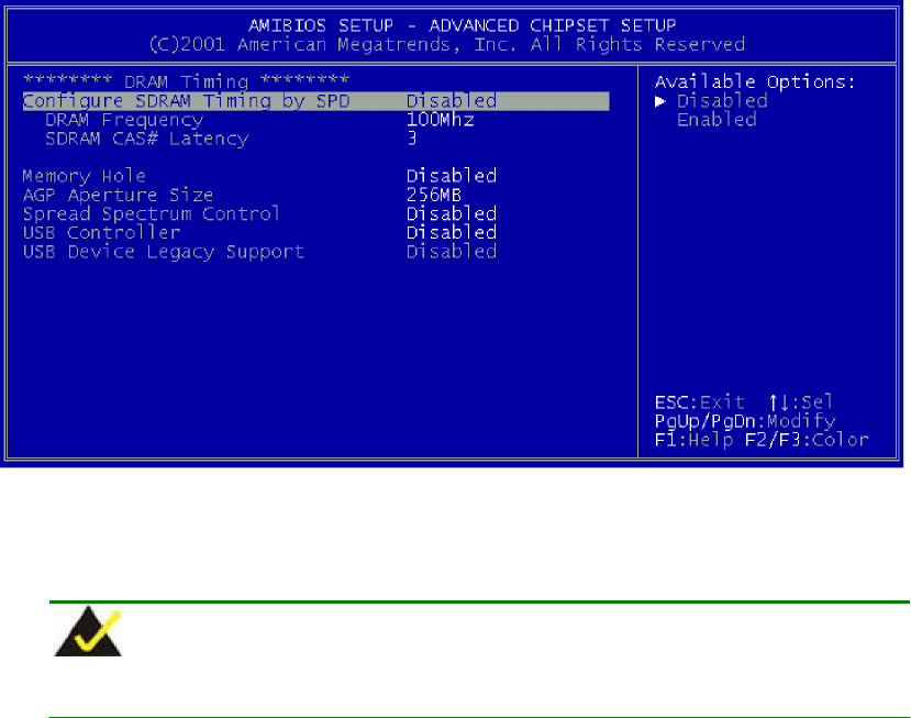
3301770
4.5 Advanced Chipset Setup Selections
„
Configure SDRAM Timing by SPD
When set to Enabled, bios will use the data from DIMM’s SPD to setup the
DRAM timing. If set to Disabled, bios will use default setting.
NOTE:
Defautl memory setting is 133MHz.
„
DRAM Frequency
This setting is setting Memory working frequency, 66/100/133 MHz.
„
Memory Hole
Some (unusual) expansion cards require access to particular memory addresses in order to
function properly. This parameter allows you to configure the appropriate area of memory
exclusively for use by these cards. The typical memory areas set for this purpose can be
"512-640KB" (the upper 128K sector of conventional memory) and "15-16MB".
Memory hole is created to prevent other devices to utilize this space.
„
Spread Spectrum Control
This option allows you to turn Spread Spectrum clocking on and off .
„
SDRAM CAS# Latency
This setting is setting Memory CAS latency
„
AGP Aperture Size
This is about the size of AGP aperture. The aperture is a portion of the PCI
4-11
3301770
Memory addresses space. Host cycles that hit the aperture range are
forwarded to the AGP without any translation
„
USB Controller
Select enable if your system contains a USB controller and you have USB
Peripherals. Otherwise, select disable.
„
USB Device Legacy Support
Enable or Disable the USB device legacy support.
4-12
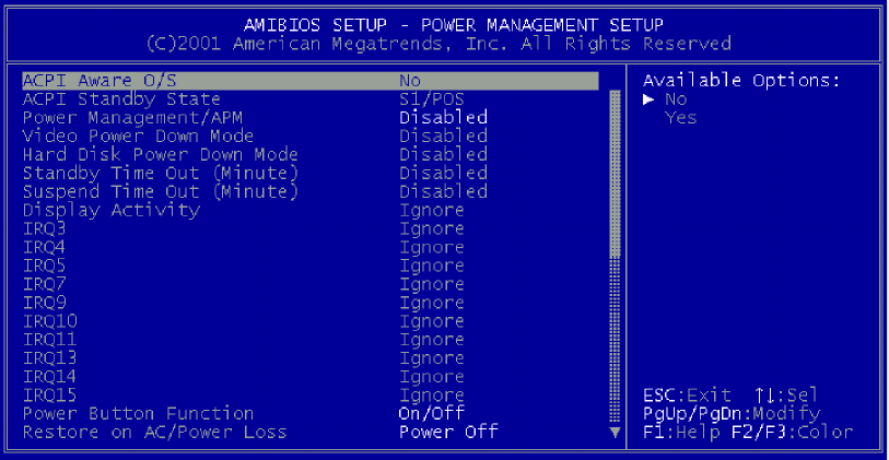
3301770
4.6 Power Management Setup Selections
„
ACPI Aware O/S
Set this value to allow the system to utilize the Intel ACPI (Advanced Configuration and
Power Interface) specification. The Optimal and Fail-Safe default setting is Yes.
„
ACPI Standby State
This option allows you to select the S1 ACPI states: S1.
The S1 state is the default setting.
„
Power Management/APM
Set this option to Enabled to run APM (Advanced Power Management).
„
Video Power Down Mode
Set this option to Enabled to allow the BIOS to power down the Video adapter and Monitor.
„
Hard Disk Power Down Mode
Set this option to Enabled to allow the BIOS to power down the Hard Disk.
„
Standby/Suspend Time Out (Minutes)
This option specifies the amount of system inactivity (in minutes) before the system will enter
Standby/Suspend state.
„
Display Activity
This option specifies if BIOS is to monitor activity on the display monitor in order to reduce
power consumption. When this option is set to “Monitor and there is no display activity for
the length of time specified in the value in the Full-On to Standby Timeout (Min) option, the
computer enters a power saving state. The settings are “Monitor or Ignore. The default
setting is “Ignore.
4-13
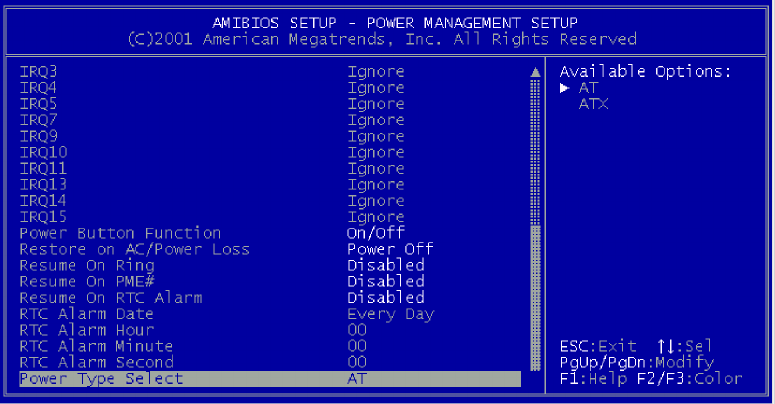
3301770
„
IRQ#
These options allow IRQ settings to be modified.
„
Power Button Function
Allows the system to go into On/Off mode or suspend mode when the power button is
pressed. Configuration options: [On/Off] [Suspend].
„
Restore on AC/Power Loss
When set to Power Off, the system goes into off state after an AC power loss. When set to
Power On, the system goes on after an AC power loss. When set to Last State, the system
goes into either off or on state Whatever was the system state before the AC power loss.
Configuration options: [Power Off] [Power On] [Last State]
„
Resume on Ring
Allows you to enable or disable RI to generate a wake event. Configuration options:
[Disabled] [Enabled]
„
Resume on PME#
Allows you to enable or disable PCI PME# to generate a wake event. Configuration options:
[Disabled] [Enabled]
„
Resume on RTC Alarm
Allows you to enable or disable RTC to generate a wake event. When this item is set to
Enabled, the items RTC Alarm Date, RTC Alarm Hour, RTC Alarm Minute, and RTC Alarm
Second appear with set values. Configuration options: [Disabled] [Enabled].
„
Power Type Select
This feature is switch of Power Type function. Configuration options: [AT] [ATX].
4-14
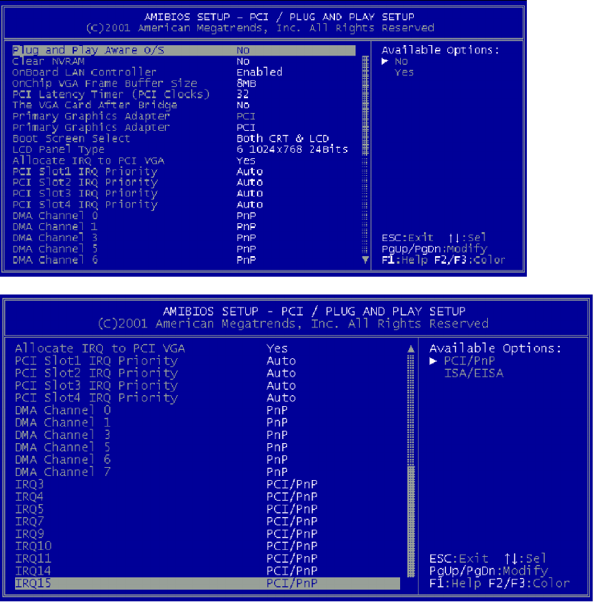
3301770
4.7 PCI / Plug and Play Setup Selections
„
Plug and Play Aware O/S
If enabled, BIOS will configure only PnP ISA boot devices (i.e. all PnP ISA cards which have
boot flag set). And PnP aware OS will configure all other devices. If disabled, BIOS will
configure all devices.
„
Clear NVRAM
Clear NVRAM during system bootup.
„
Onboard LAN Controller
Allows you to enable/disable the onboard LAN function.
4-15
3301770
„
Onchip VGA Frame Buffer Size
This setting instructs the BIOS to reserve the specified amount of memory for the internal
video controller.
„
PCI Latency Timer
Value in units of PCI clocks for PCI device latency timer register
PCI Latency Timer [64]
Configuration options: [32] [64] [96] [128] [160] [192] [224] [248]
„
VGA Card After Bridge
Factory preserved function. Leave this option unchanged.
„
Primary Graphics Adapter
Allows you to select a primary adapter in the situation when both AGP and PCI graphics
controllers are used. It decides which controller gets priority when booting.
„
Boot Screen Select
This item provides two options with display connection. You may let the BIOS to determine
the connected display(s) or manually assign Both CRT & LCD displays.
„
DMA Channel 0, 1, 3, 5, 6, 7
The option allows the user to specify the bus type used by each DMA channel. The settings
are PnP or ISA/EISA.
„
IRQ3, 4, 5, 7, 9, 10, 11, 14, 15
The option specifies the bus that the specified IRQ line is used on. The user can reserve
IRQs for legacy ISA adapter cards whilst determining if AMIBIOS should remove an IRQ from
the pool of available IRQs passed to devices that are configurable by the system BIOS. The
available IRQ pool is determined by reading the ESCD NVRAM. If more IRQs need to be
removed from the pool, the user can optionally reserve the IRQ by assigning an ISA setting to
it. Onboard I/O is configured by AMIBIOS. All IRQs used by onboard I/O are configured as
PCI/PnP.
„
Allocate IRQ to PCI VGA
NO: Does not assign IRQ to PCI VGA card even if card requests an IRQ
YES: Assigns IRQ to PCI VGA card if card requests IRQ
Allocate IRQ to PCI VGA [Yes]
Configuration options: [No] [Yes]
„
PCI Slot# IRQ Priority
This option allows you to manually configure a fixed interrupt request value for a specific PCI
slot. This setting may apply when problems occur with PCI card driver or interrupt conflicts.
„
LCD Panel Type
System BIOS and custom drivers are kept in a Flash ROM device. Because the system is
highly integrated, the Flash chip holds system BIOS, VGA BIOS, and network ROM image.
This BIOS configuration option provides direct access to the display panel setting.
4-16

3301770
NOTE:
It is recommended not to change the rest of the BIOS menu options under this
category. The default setting will work properly for the majority of applications.
4.8 Peripheral Setup Selections
„
OnBoard FDC
This option allows you to enable/disable the onboard floppy disk controller.
„
OnBoard Serial Port#
This feature allows you to disable the onboard serial port or to manually select the I/O
address and IRQ for it.
„
Serial Port2 Mode
This feature allows you to assign serial port2 to function as the IrDA device connector.
„
On-Board Parallel Port
This option specifies the base I/O port address of the parallel port on the motherboard. The
settings are Disabled, 378h, 278h, or 3BCh.
„
Parallel Port Mode
This option specifies the parallel port mode. The settings are Normal, Bi-Dir, ECP, and EPP.
Normal:
The normal parallel port mode is used.
4-17
3301770
Bi-Dir:
Use this setting to support bi-directional transfers on the parallel port.
EPP:
The parallel port can be used with devices that adhere to Enhanced Parallel Port (EPP)
specifications. EPP uses the existing parallel port signals to provide asymmetric
bi-directional data transfer driven by the host device.
ECP:
The parallel port can be used with devices that adhere to Extended Capabilities Port (ECP)
specifications. ECP uses the DMA protocol to achieve data transfer rates of up to 2.5
Megabits per second, and provides symmetric bi-directional communication.
„
Parallel Port IRQ
This option specifies the IRQ used by the parallel port. The settings are (IRQ) 5, (IRQ) 7.
„
Parallel Port DMA Channel
This option is only available if the setting for the Parallel Port Mode option is set to ECP. It sets
the DMA channel used by the parallel port. The available settings are DMA Channel 0, 1, or 3.
„
OnBoard IDE
This option is factory reserved. Do not change its value.
„
OnBoard AC’97 Audio
This option allows you to enable or disable the onboard audio functionality.
4-18
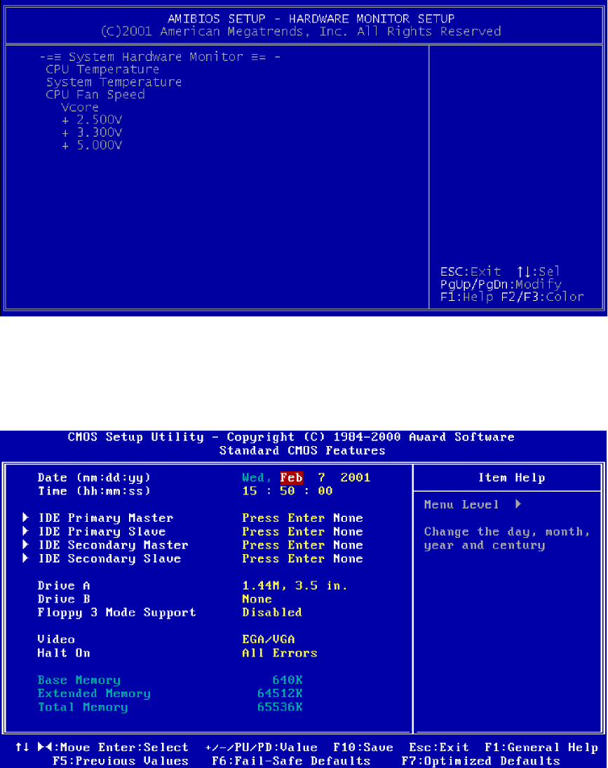
3301770
4.9 Hardware Monitor Setup Selections
This menu screen provides access to the readings of CPU temperature, fan speed, and voltage
sensors.
4.10 Auto-Detect Hard Drives
When the Auto-detect command is executed, system BIOS will automatically detect
Primary IDE bus master/slave, Secondary IDE bus master/slave, and floppy drive
parameters.
4-19

3301770
4-20

3301770
Appendix
A
Watchdog Timer
A-1
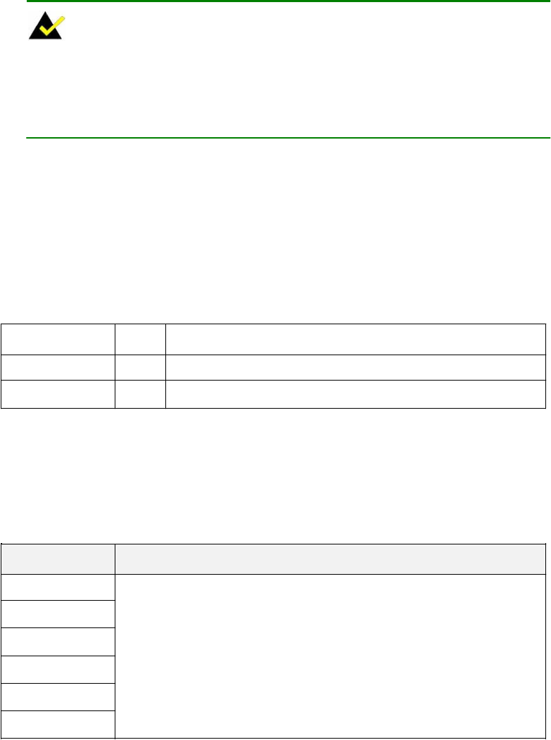
3301770
NOTE:
The following discussion applies to DOS environment. It is recommended
you contact GAI support or visit our website for specific drivers for more
sophisticated operating systems, e.g., Windows and Linux.
The Watchdog Timer is a device to ensure that standalone systems can always recover from
catastrophic conditions that cause the CPU to crash. This condition may have occurred by EMI
or a software bug. When the CPU stops working normally, hardware on the board will perform
hardware reset (cold boot) to bring the system back to a known state.
Three I/O ports control the Watchdog Timer:
443 Write Set Watchdog time period
443 (hex) Read Enable the refresh to the Watchdog Timer
043/843 (hex) Read Disable the Watchdog Timer
Table -1 I/O Ports to Watchdog Timer
Prior to enable the Watchdog Timer, users have to define the Timer first. The output data is a
value of time interval and the range of the value is from 01 (hex) to FF (hex) and the range for time
interval ranges from 1 second to 255 seconds.
DATA TIME INTERVAL
01 1 sec
02 2 sec
03 3 sec
04 4 sec
- - - - - -
FF 255 sec
Table -2 Watchdog Timer Output Data
This will enable and activate the countdown timer which eventually time out and reset the CPU to
ensure that this reset condition does not occur; the Watchdog Timer must be periodically
refreshed by reading the same I/O port 043/843H and 443H. This must be done within the time
A-2

3301770
out period that is selected by software, please refer to the example program.
A tolerance of at least 5% must be maintained to avoid unknown routines within the operating
system (DOS), such as disk I/Os that can be very time consuming. Therefore, if the timeout
period has been set to 10 seconds, the I/O port 443H must be read within 7 seconds.
NOTE:
When exiting a program it is necessary to disable the Watchdog Timer,
otherwise the system will reset.
Example Assembly Program:
TIMER_PORT = 443H
TIMER_START = 443H
TIMER_STOP = 843H
;;INITIAL TIME PERIOD COUNTER
MOV DX, TIME_PORT
MOV AL, 8: ;;8 SECONDS
OUT DX, AL
;;ADD YOUR APPLICATION HERE
MOV DX, TIMER START
IN AL, DX. ;;START COUNTER
ADD YOUR APPLICATION HERE
W_LOOP:
MOV DX, TIMER_START
IN AL, DX. ;RESTART COUNTER
;ADD YOUR APPLICATION HERE
CMP EXIT_AP, 0
JNEW_LOOP
MOV DX, TIMER_STOP
A-3
3301770
IN AL, DX
;;EXIT AP
A-4

3301770
Appendix
B
Connecting ATX
Power Supply
B-1

3301770
The following notes show how to connect ATX Power Supply to the embedded board.
1. Using ATX Power Switch
Step 1. Disconnect the AC cord of the Power Supply from the AC source to prevent
sudden electric surge to the board.
Figure -1 ATX Power Connection
Step 2. Connect an ATX power button switch (see the diagram above) to the ATX
ON/OFF switch connector (power button). And connect the power cable from
20-pin ATX power supply to the CN1 4P and the CN2 SBVCC ATX feature
connectors. The connection can be done using the adapter (ATX-to-4P)
cable.
B-2
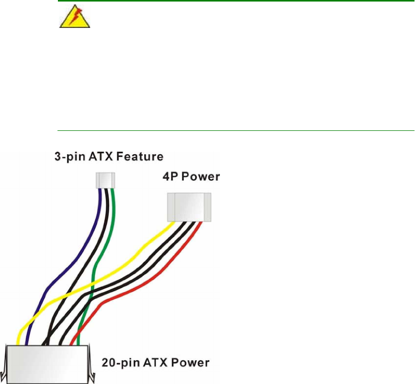
3301770
WARNING!
The new power adapter cable has its “Ground” pin removed from the
3-pin ATX feature connector. If you connect the power feature
connector cable previously provided by GAI, you will destroy the
3301770 board.
Figure BT-2 ATX Power Adapter Cable
Step 3. To turn on the system press the button once. To turn off the power supply press
the ATX power switch button for about 4 seconds.
2. Using AT Power Supply
The connection to an AT power supply is as simple as connecting a 4P power connector
to CN1. Power on or off is controlled by the power switch on the AT power supply.
B-3

3301770
This page is intentionally left blank
B-4

3301770
Appendix
C
ALi® RAID for SATA
C-1
3301770
1. Introduction
The ALi M5283 is a highly integrated disk drive controller that is capable of managing Parallel-ATA
and Serial-ATA interface hard disk drives. The ALi controller supports PATA UDMA transfer mode
up to mode 6 and SATA 1.0 disk drives. The ALi M5283 also comes with cost-effective RAID
functionalities that can be used to increase data read/write speed and to provide protection to data
by distributing mirrored duplicates of data onto two disk drives (RAID1).
CAUTION!
You must properly configure the associated BIOS settings before the Ctlr+A
key combination can take effect. Please refer to Chapter 4 AMI BIOS
Setup, the discussions of the associated configurations for more details.
SATA disk drive support must be initiated under the following two BIOS
sub-menus.
1. Boot -> Onboard SATA ROM
2. Chipset -> Southbridge Chipset Configuration
You will not be able to access the ALi configuration utility unless you have
properly initiated the SATA disk drive support in the AMI BIOS configuration
utility.
CAUTION!
A configured RAID volume (which may consist of multiple hard drives)
appears to an operating system as a contingent storage space. Your
operating system will not be able to distinguish the physical disk drives
contained in a RAID configuration.
Precautions:
1. One key benefit a RAID configuration brings you is that a single hard drive can fail within a
RAID array without damaging your data. With RAID1 array, you can replace a failed drive
and restore your RAID configuration.
C-2
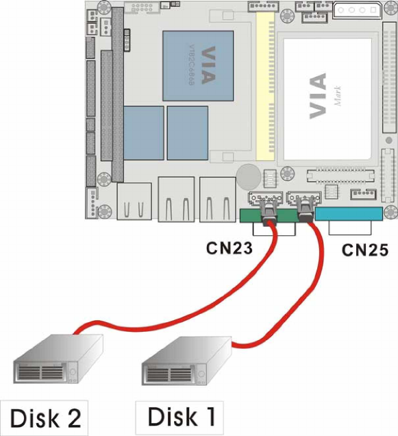
3301770
However, if you replace the wrong drive when you are trying to remove a failed one,
irrecoverable data loss will occur! It is therefore strongly recommended to mark the
physical connections of all of your SATA disk drives. If a drive member of a RAID array
should fail, you will then be able to correctly locate a failed drive.
For example, you may specify the drive locations by attaching stickers to the drive bays. You
need a reminder if the cabling does not match the physical locations of hard drives.
2. It is also crucial that you do not accidentally disconnect the SATA drive cables. Carefully
route your cables within the chassis to avoid system down time.
2. Features and Benefits
„
Supports RAID levels 0, 1, and JBOD
„
Supports the connectivity to two disk drives
„
The supported Operating Systems include: Windows 98/Me, Windows 2000, and
Windows XP
„
Windows-based software for RAID management
C-3

3301770
3. SATA-ALi RAID Driver
CAUTION!
Because of the inherent limitations by system chipset, the ALi M5283
SATA and RAID controller is implemented as a device that requires you
to provide device driver during the Windows installation process. To
successfully install the device driver, please carefully read the following
instructions.
The ALi driver is especially required if SATA drives are the only hard disk drives in your system.
Otherwise the Windows installation program may fail to locate your hard drives whether you
configure your SATA disk drives into RAID volumes or use them as individual disk drives.
The system BIOS can identify SATA disk drives, but cannot control their operation. The separately
installed driver therefore is necessary.
ALi SATA Controller Driver Installation Steps
- During Windows XP Installation
Step 1. Enable SATA ROM using the BIOS configuration utility. The SATA ROM option is
provided in the Southbridge chipset menu. The process has been detailed in
Chapter 4.
Step 2. Locate the ALi installation driver folder within the Utility CD that came with your
motherboard.
Step 3. Copy files under a sub-directory named “SATA50XX” (taking Windows XP installation
as the example) to the root directory of floppy diskette (labeled driver diskette). The
file names are listed below:
„
disk1
„
5283096D.bin
„
txtsetup.oem
Also copy the OS option directory “win98_me”, “win_nt”, or “win_xp”, and related
driver files in each directory.
C-4
3301770
Step 4. Boot from Windows installation CD-ROM (this requires you to set CD-ROM as the 1
st
Boot Device), when the Windows XP Setup blue screen appears and prompts users to
Press F6 if you need to install third-party SCSI or RAID driver, please press the F6 key.
Step 5. The setup program will continue, later when the setup program prompts users to
specify additional adapters, please press the S key.
Step 6. Then the setup program will prompt user to insert the driver diskette. Please insert
the driver diskette your prepared previously, and then press ENTER to continue.
Step 7. The follow-up window will list out the installation choices, please select ALi
SATA/RAID Controller for Windows XP and press ENTER to continue.
Step 8. The follow-up window will list out the devices to be installed, in which selected ALi
controller(s) should be included.
Step 9. Repeat step 5, but select ALi ATA/RAID Controller at step 7. If both controllers are
installed, go to next step.
Step 10. If users want to install other devices, please operate at this time. If all devices have
been successfully installed, please go to next step.
Step 11. Press Enter to continue Windows XP setup.
Installation Steps under Existing Windows XP
After Windows XP is started, Windows system will automatically find the newly installed adapter
and prompt user to install its driver. Please follow these steps to install the driver:
Step1. When the Found New Hardware Wizard windows appear(Mass Storage Controller),
select Install from a list or specify location(Advanced) and click Next to continue.
Step 2. In the follow-up window, please select "Don't search, I will choose the driver to install",
then click Next to continue.
C-5
3301770
Step 3. In the follow-up window, please select SCSI and RAID controllers, and then click Next
to continue.
Step 4. In the follow-up window, click Have Disk..., then insert the driver diskette and type in
the driver location: e.g., a CD-ROM, then click OK to continue.
Step 5. In the follow-up window, select ALi SATA/RAID Controller, then click Next to continue.
Step 6. Confirm the follow-up windows and click the Finish button to continue.
Step 7. Please "confirm" the Digital Signature Not Found window when it appears, when
finished, please restart the computer.
Step 8. Repeat step 1, but select ALi ATA/RAID Controller at step 4.
4. Accessing the ALi RAID Utility
If the SATA ROM configuration options in system BIOS have been properly configured, the RAID
BIOS version and disk drive information should appear after system POST screen.
The BIOS disk drive information should look like the following:
ALi RAID BIOS V1.XX
(c) ALi Corporation 2005, All Rights Reserved.
Identifying IDE drives…
Channel 1 Master: Maxtor xxxxxx
Channel 2 Master: Maxtor xxxxxx
Press Ctrl-A to enter ALi RAID BIOS setup utility
To enter the RAID configuration utility, press ‘Ctrl’ and ‘A’ keys simultaneously.
C-6
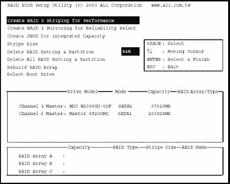
3301770
1. RAID BIOS Setup Menu:
The Serial ATA RAID volume may be configured using the RAID Configuration utility stored
within the ALi RAID controller ROM. The BIOS configuration screen is divided into three
major functional areas: Main Functional Menu, Drive Selection Menu, and a list for the
configured RAID arrays.
2. RAID Options:
2.1 Create RAID0 Striping for Performance
Step 1. To create a RAID0 array, use your arrow keys to highlight and press Enter to
activate this item. An ‘S’ flashing character will appear at the Drive
Selection Menu where you can choose the member drives to be included in
the RAID0 array.
Step 2. Use the Space key to select members of the RAID0 RAID configuration.
The flashing cursor should change to a lower case ‘s’ character once any of
the connected disk drives has been selected. Follow the same method to
select another member drive.
C-7

3301770
Step 3. You should then be prompted by a “Create RAID0(Y/N)” confirm box.
Step 4. Press Y and then some necessary information will be written to the selected
disk drives.
WARNING!
All data previously stored on the member drives of a RAID configuration will
be destroyed during the RAID initialization process. If you use “used” drives
to create a RAID array, make you have moved or backed up your data before
creating a RAID array out of these disk drives.
Step 5. Next you will be prompted to enter a nickname for the created array.
Upper and lower case alphabetic, numeric, space, and underscore
characters are all applicable for naming an array.
Step 6. Once an array is successfully created, it will be listed in the list of the
configured arrays.
C-8
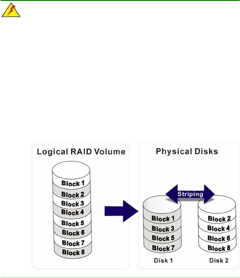
3301770
NOTE:
1. To reduce the chance of losing data, ALi imposed certain limitations on the
RAID configuration options. For example, Parallel-ATA drives connected
on the same IDE channel cannot be selected as the members of a RAID0
array. Mixing Parallel- and Serial-ATA disk drives in a RAID0 array should
also be avoided.
2. Always use disk drives of the same capacity to create a RAID array. The
excessive capacity of a larger disk drive cannot be utilized because data
stripes are equally distributed across all members of a RAID array. The
operational concept is diagrammed below.
C-9

3301770
2.2 Create RAID1 Mirroring for Reliability
Step 1. To create a RAID1 array, use your arrow keys to highlight and press Enter to
activate this item. An ‘M’ flashing character will appear at the Drive
Selection Menu where you can choose the member drives to be included in
the RAID1 array.
Step 2. Use the Space key to select members of the RAID1 RAID configuration.
The flashing cursor should change to a lower case ‘m’ character once any
of the connected disk drives has been selected. Follow the same method
to select another member drive.
Step 3. You should then be prompted by a “Create RAID1(Y/N)” confirm box.
Step 4. Press Y and then some necessary information will be written to the selected
disk drives.
WARNING!
All data previously stored on the member drives of a RAID configuration will
be destroyed during the RAID initialization process. If you use “used” drives
to create a RAID array, make you have moved or backed up your data before
creating a RAID array out of these disk drives.
Step 5. Next you will be prompted to provide a nickname for the created array.
Upper and lower case alphabetic, numeric, space, and underscore
characters are all applicable for naming an array.
Step 6. Once an array is successfully created, it will be listed in the list of the
configured arrays.
Step 7. Lastly a prompt will require you to proceed with drive copy. The Source
and Destination drives will be indicated as “M” and “m” in the Drive
Selection Menu.
C-10
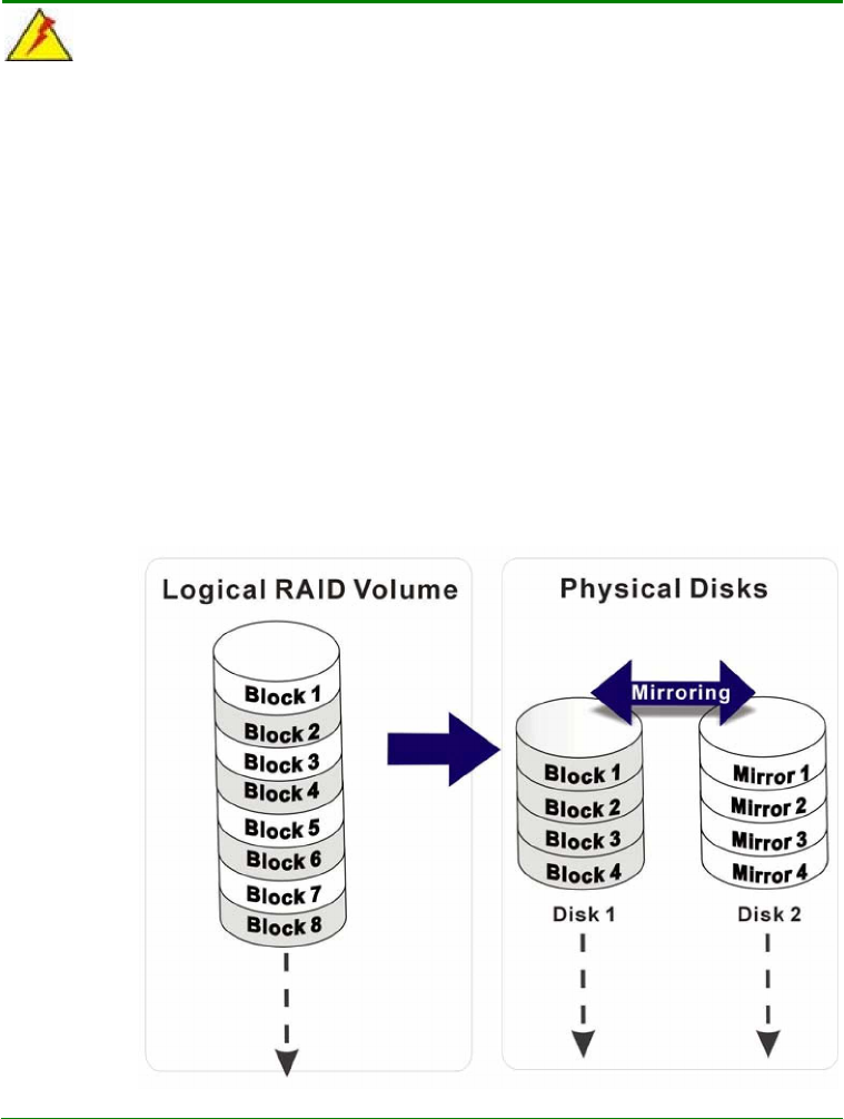
3301770
NOTE:
1. To reduce the chance of losing data, ALi imposed limitations on the
RAID configuration options. For example, Parallel-ATA drives
connected on the same IDE channel cannot be selected as the
members of a RAID1 array. Mixing Parallel- and Serial-ATA disk drives
in a RAID1 array should also be avoided.
2. Always use disk drives of the same capacity to create a RAID array.
The excessive capacity of a larger disk drive cannot be utilized because
data mirrors are equally distributed across corresponding members of
drive pairs within a RAID array. The operational concept is
diagrammed below.
2.3 Create JBOD for Integrated Capacity
Step 1. JBOD stands for “Just a Bunch of Drives.” JBOD provides neither
performance gains nor data redundancy. To create a JBOD array, use
your arrow keys to highlight and press Enter to activate this item. A ‘J’
C-11

3301770
flashing character will appear at the Drive Selection Menu where you can
choose the member drives to be included in the JBOD.
Step 2. Use the Space key to select members of the JBOD configuration. The
flashing cursor should change to a lower case ‘j’ character once any of the
connected disk drives has been selected. Follow the same method to
select another member drive. The maximum number of member drives in
a JBOD is four and the minimum is two.
Step 3. You should then be prompted by a “Create RAID1(Y/N)” confirm box.
Step 4. Press Y and then some necessary information will be written to the selected
disk drives.
WARNING!
All data previously stored on the member drives of a RAID configuration will
be destroyed during the RAID initialization process. If you use “used” drives
to create a RAID array, make you have moved or backed up your data before
creating a RAID array out of these disk drives.
Step 5. Next you will be prompted to provide a nickname for the created array.
Upper and lower case alphabetic, numeric, space, and underscore
characters are all applicable for naming an array.
Step 6. Once an array is successfully created, it will be listed in the list of the
configured arrays.
C-11

3301770
NOTE:
To reduce the chance of losing data, ALi imposed limitations on the RAID
configuration options. For example, Parallel-ATA drives connected on the
same IDE channel cannot be selected as the members of a RAID1 array.
Mixing Parallel- and Serial-ATA disk drives in a RAID1 array should also be
avoided.
2.4 Stripe Size
The change to stripe size takes effect on RAID0 arrays. Configurable options are:
64K (default), 32K, 16K, 8K, and 4K. If you can be certain that your I/Os to the hard
drives are small and randomly occurred, you can select a small stripe size. If your
I/Os are mostly large and come in sequential orders, e.g., A/V playback and editing
applications, choose a larger stripe size.
The default value, 64K, should be appropriate for most applications.
2.5 Delete RAID Setting & Partition
Step 1. To delete an existing RAID configuration, use your arrow keys to highlight
and press Enter to activate this item. An ‘E’ flashing character will appear
at the Drive Selection Menu where you can choose the member drives to be
removed from an existing configuration.
Step 2. You should then be prompted by “Data on RAID drives will be erased
(Y/N)?”.
Step 3. Press Y and then the RAID configuration will be invalidated.
C-13
3301770
WARNING!
If you delete a RAID configuration, all data previously stored on the member
drives of the RAID configuration will be destroyed.
2.6 Delete All RAID Setting & Partition
Step 1. To delete all existing RAID configurations, use your arrow keys to highlight
and press Enter to activate this item.
Step 2. You should then be prompted by “Data on RAID drives will be erased
(Y/N)?”.
Step 3. Press Y and then all existing RAID configurations will be invalidated.
WARNING!
If you delete a RAID configuration, all data previously stored on the member
drives of the RAID configuration will be destroyed.
C-14
3301770
2.7 Rebuild RAID Array
This function allows you to rebuild a RAID array if a member of a RAID configuration
should fail. Neither RAID0 nor JBOD provides data redundancy. Therefore, this
option only applies to RAID1 arrays. This item takes effect when a member of a
RAID1 configuration has failed.
Step 1. To delete all existing RAID configurations, use your arrow keys to highlight
and press Enter to activate this item.
Step 2. An “R” flashing character should appear at the list of existing arrays.
Step 3. The source and destination drives will be displayed.
Step 4. Press Y to begin the rebuild process.
Step 5. During the rebuild process, the rebuild progress will be indicated by a status
bar. Rebuild consumes considerable system resources and the time
required for rebuilding a RAID array may vary depending on the size of
stored data, disk drive capacity, and drive performance.
2.8 Select Boot Drive
Step 1. To select a Boot drive, use your arrow keys to highlight and press Enter to
activate this item.
Step 2. An “A” flashing character should appear at the Drive Selection Menu.
Step 3. Press Enter or the Space key to finish the configuration.
C-15

3301770
This page is intentionally left blank
C-16

3301770
Index
I-1
3301770
00,32k Shadow, 4-9
10/100BaseT Ethernet, 2-31
1st Boot Device, 4-7
2D/3D/Video Accelerator, 2-4
2nd Boot Device, 4-7
32Bit Mode, 4-6
3rd Boot Device, 4-7
4P power, 1-3, 2-10
AC ’97, 1-8
Accessories, 3-13
ACPI Aware O/S, 4-13
ACPI Standby State, 4-13
Adapter Cable, B-3
AGP Aperture Size, 4-11
AGP/SVGA, 2-3
Airflow, 3-3
ALi, C-6
Allocate IRQ, 4-16
AT Power, B-3
AT/ATX-compatible, 1-2
ATX ON/OFF, 2-12
ATX Power, B-1
ATX Power Feature, 2-12
audio, 1-3, 2-10
Audio, 1-7, 2-15, 3-10
Audio CD_IN, 1-3, 2-10, 2-16
backplane, 2-2
Battery Connector, 2-14
BIOS, 1-6, 4-1
BIOS Cacheable, 4-9
Block Diagram, 2-5
Block Mode, 4-6
Board Overview, 1-5
Boot Drive, C-15
Boot from LAN, 4-8
Boot To OS/2, 4-8
BootUp Num-Lock, 4-8
Cables Included, 3-13
CF II socket, 2-6
chassis, 2-2
Chipset, 1-6
Clear CMOS, 3-6
Clear NVRAM, 4-15
CN1, 2-11
CN10, 2-16
CN11, 2-18
CN12, 2-19
CN13, 2-19
CN14, 2-20
CN15, 2-21, 3-9
CN16, 2-22
CN17, 2-23
CN19, 2-24, 2-31
CN2, 2-12, 2-13
CN20, 2-24, 2-31, 3-11
CN21, 2-31, 3-11
CN22, 2-32
CN23, 2-24
CN24, 2-25
CN25, 2-24
I-2
3301770
CN26, 2-32, 3-10
CN27, 2-25
CN28, 2-26, 3-10
CN29, 2-26, 3-10, 3-11
CN3, 2-13
CN30, 2-27
CN31, 2-29
CN32, 2-30
CN5, 2-14
CN6, 2-14
CN7, 2-14
CN8, 2-15
CN9, 2-16
coin cell, 2-10
COM1, 1-3, 2-10, 2-32, 3-10
COM2, 1-3, 2-10, 2-22, 2-23, 3-10
COM2 Signal, 3-7
Compact flash, 1-4, 2-11
Compact Flash, 2-30
Compact Flash Disk, 1-6, 3-9
configuration jumpers, 2-9
Configuration Jumpers, 3-5
CoreFusion, 1-4, 2-6
CPU, 1-6, 2-2
CPU fan, 1-3, 2-10
CRT VGA, 3-10
Digital I/O, 2-20
Display Activity, 4-13
Display Controller, 1-6
Display Mode, 2-4
DOS environment, A-2
DRAM Frequency, 4-11
EEPROM, 1-7
electrostatic discharge, 3-2
ESD, 3-2
Ethernet, 3-11
Ethernet interface, 1-6
Ethernet port, 1-3, 2-10
Ethernet Port LED, 2-32
external interfaces, 2-8
external VCC, 1-3
external -VCC, 2-10
External VCC Power, 2-18
failed drive, C-2
Fan Connector, 2-13
FDD Interface, 1-6
FDD1, 3-9
Flat panel display, 3-10
Flat Panel Display, 2-26
floppy, 1-4, 2-11
Floppy, 2-29, 3-9
Floppy A, B, 4-5
Floppy Drive Seek, 4-7, 4-8
Floppy Drive Swap, 4-8
Form Factors, 1-7
FPC connector, 2-29
Frame buffer, 2-4
Front Panel, 2-31
general purpose I/Os, 1-3, 2-10
Hard Disk Drives, 3-8
Hard Disk Power Down, 4-13
Hardware monitor, 1-7
Hardware Monitor, 2-6
heatsink, 1-4, 2-2
Humidity, 2-7
IDE, 1-4, 2-11, 2-27, 3-8
I-3
3301770
IDE Interface, 1-6
Important Features, 2-6
Installation, 3-2
internal USB, 1-3
Internal USB, 2-25
Inverter control, 1-3
IrDA, 1-4, 2-6, 2-11, 2-25
IrDA port, 1-7
IRQ, 4-16
IRQ#, 4-14
IVTC, 2-13
JBOD, C-11
JP1, 2-24, 3-6
JP2, 3-7
JP3, 3-7
Jumper Settings, 3-5
Keyboard/Mouse, 2-23
keyboard/mouse connector, 1-3, 2-10
L1 Cache, 4-8
L2, 2-6
L2 Cache, 4-9
LBA Mode, 4-5
LCD panel, 1-4
LCD Panel, 3-10
LCD Panel Inverter Backlight Control,
2-13
LCD Panel Type, 4-16
LED, 2-10, 2-14
Level 2, 2-3
Lithium 3V, 1-3, 2-10
LVDS LCD, 2-26
LVDS Panel Display, 2-26
LVDS type LCD, 3-10
LVDS/TTL, 2-11
Mechanical Diagrams, 3-4
Memory, 1-6, 2-3
Memory Hole, 4-11
Mounting Holes, 3-4
multimedia, 1-2
OnBoard AC 97, 4-18
OnBoard FDC, 4-17
OnBoard IDE, 4-18
Onboard LAN Controller, 4-15
On-Board Parallel Port, 4-17
OnBoard Serial Port#, 4-17
Onchip VGA Frame Buffer, 4-16
Operating Temperature, 1-7
OSes, 1-4
0
Packing List, 1-8
parallel, 2-10
Parallel, C-9
parallel port, 1-3
Parallel Port, 1-7, 2-21, 3-9
Parallel Port DMA, 4-18
Parallel Port IRQ, 4-18
Parallel Port Mode, 4-17
Password Check, 4-8
PC/104, 1-3, 1-7, 2-6, 2-16
PC133, 2-2
PCI, 1-6
PCI Latency Timer, 4-16
PCI Slot# IRQ Priority, 4-16
PIO Mode, 4-6
Plug and Play, 4-15
Power 4P, 2-11
power adapter cable, B-3
I-4
3301770
Power and HDD LED, 2-14
Power Button, 4-14
Power consumption, 2-7
Power Management, 4-13
Power ON/OFF Button, 2-19
Power Supply, 1-7
Power Switch, B-2
Power switch button, 1-3, 2-10
Power Type Select, 4-14
Primary Display, 4-8
Primary Graphics Adapter, 4-16
Primary/Secondary Master, 4-5
ProSavage4, 2-3
PS/2 Mouse Support, 4-8
PS-ON/ATX, 2-10
PS-ON/ATX feature, 1-3
PXE, 3-11
1
Quick Boot, 4-7
2
RAID, C-1
RAID0, C-7
RAID1, C-10
Realtek, 2-6
Rebuild, C-15
Reset button, 1-3, 2-10
Reset Button, 2-19
resolutions, 1-4
Restore on AC, 4-14
Resume on PME#, 4-14
Resume on Ring, 4-14
Resume on RTC Alarm, 4-14
RJ-45, 2-31
RoHS, 2-6
ROM BIOS, 4-2
RS-232, 3-7
RS-422, 3-7
RS-485, 3-7
3
S.M.A.R.T., 4-8
SATA-ALi RAID, C-4
SBVCC, 2-12
SDRAM CAS#, 4-11
SDRAM Timing, 4-11
Serial ATA, 1-3, 2-10, 2-24
Serial ports, 1-7
Serial-ATA, C-9
SODIMM, 1-2, 2-6
SO-DIMM, 1-3, 2-10
SODIMM Socket, 2-14
Soldering Side, 3-8
Spread Spectrum Control, 4-11
Standard CMOS, 4-5
Standby/Suspend Time Out, 4-13
Stripe Size, C-13
System Keyboard, 4-8
System Monitoring, 1-8
4
TFT, 2-6
TFT LCD, 1-4, 2-3, 2-11, 2-26
TFT panel, 2-4
Try Other Boot Devices, 4-7
5
Unpacking, 3-3
USB, 1-3, 1-7, 2-10, 2-25, 2-31, 3-12
USB Controller, 4-12
USB Device Legacy, 4-12
USB ports, 2-6
USB01, 3-12
6
VGA, 1-4, 2-11, 2-32
VGA/LCD Interface, 2-4
I-5
3301770
VIA MARK, 1-4
VIA processor, 1-2
Video Power Down, 4-13
Virus Protection, 4-6
VT82C686B, 2-2
7
Watchdog Timer, 1-7, 2-7, A-1
I-6

Any advice or comments about our products and service, or anything we can
help you with please don’t hesitate to contact with us. We will do our best to support
you for your products, projects and business
Global American Inc.
Address: 17 Hampshire Drive
Hudson, NH 03051
TEL: Toll Free (U.S. Only) 800-833-8999
(603)886-3900
FAX: (603)886-4545
Website: http://www.globalamericaninc.com
E-Mail: salesinfo@globalamericaninc.com