Vitelcom Mobile Technology USA TSM501 Single Band CDMA Cellular Phone User Manual
Vitelcom Mobile Technology USA, Inc. Single Band CDMA Cellular Phone
Contents
- 1. User manual
- 2. Service manual
Service manual
9LWHOFRP0RELOH7HFKQRORJ\6$ 3URSULHWDU\DQG&RQILGHQWLDO - 1 -
V
V
I
I
T
T
E
E
L
L
C
C
O
O
M
M
M
M
O
O
B
B
I
I
L
L
E
E
T
T
E
E
C
C
H
H
N
N
O
O
L
L
O
O
G
G
Y
Y
S
S
.
.
A
A
.
.
TSM501/ VTL501 Service Manual
Prepared by: Kenn Lee Edited by K.H.Kim
Approved by: Sam Her
Version: 1.0
Date: 10/12/04
9LWHOFRP0RELOH7HFKQRORJ\6$ 3URSULHWDU\DQG&RQILGHQWLDO - 2 -
V
V
I
I
T
T
E
E
L
L
C
C
O
O
M
M
M
M
O
O
B
B
I
I
L
L
E
E
T
T
E
E
C
C
H
H
N
N
O
O
L
L
O
O
G
G
Y
Y
S
S
.
.
A
A
.
.
Document Status History
Version Date Pages Changes Signatures
1.0 08/12/04 72 First Version

9LWHOFRP0RELOH7HFKQRORJ\6$ 3URSULHWDU\DQG&RQILGHQWLDO - 3 -
V
V
I
I
T
T
E
E
L
L
C
C
O
O
M
M
M
M
O
O
B
B
I
I
L
L
E
E
T
T
E
E
C
C
H
H
N
N
O
O
L
L
O
O
G
G
Y
Y
S
S
.
.
A
A
.
.
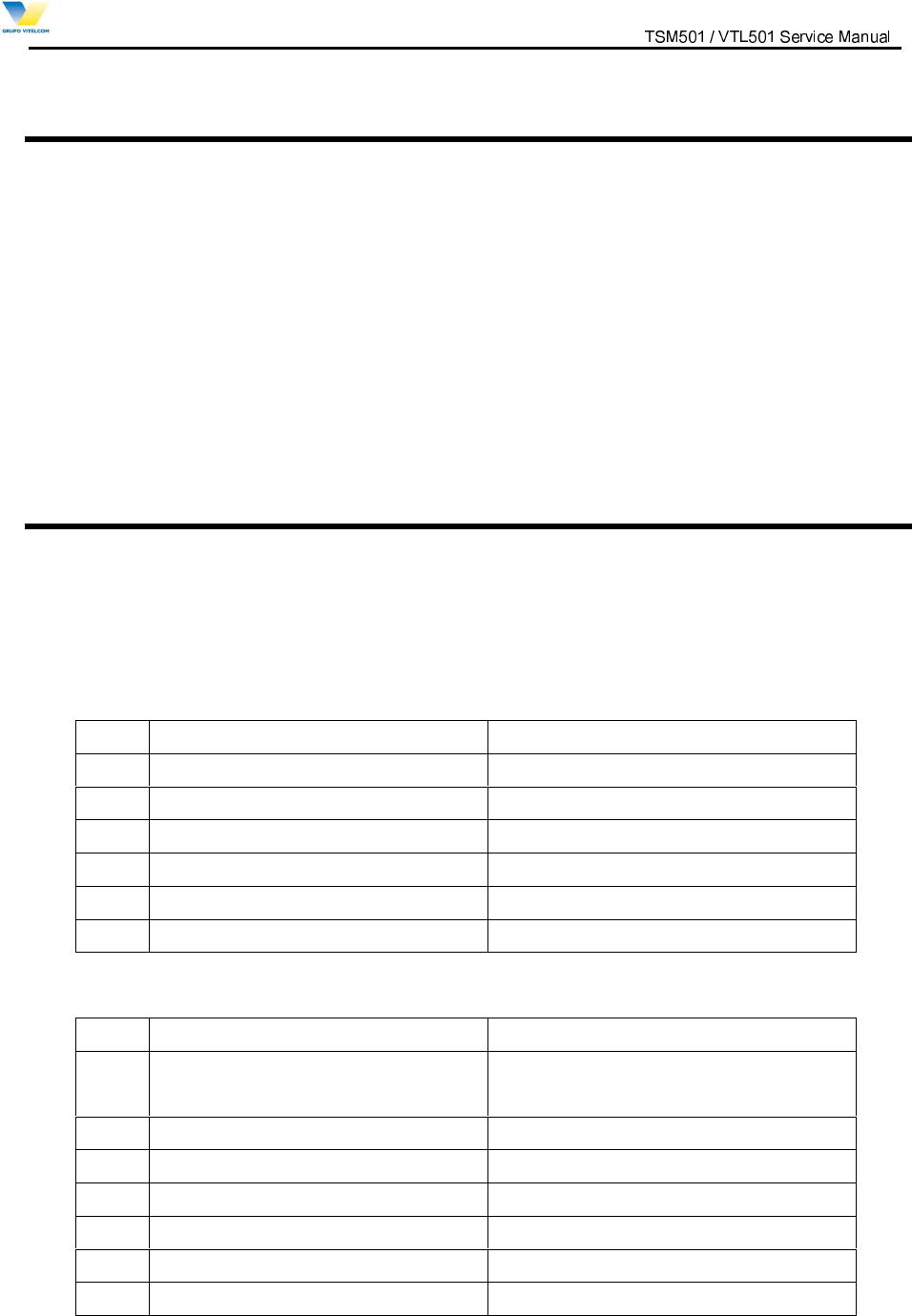
TABLE OF CONTENTS
1. INTRODUCTION.......................................................................................................................................................4
2. SPECIFICATION.......................................................................................................................................................4
2.1 PRODUCT STRUCTURE ............................................................................................................................. 4
2.2 TSM501 / VTL501 SPECIFICATIONS......................................................................................................... 4
2.3 BATTERY SPECIFICATIONS ........................................................................................................................ 5
2.4 AC CHARGER SPECIFICATIONS ................................................................................................................. 5
3. MENU TREE..............................................................................................................................................................6
4. TECHNICAL DESCRIPTION ................................................................................................................................10
4.1 OVERVIEW............................................................................................................................................. 10
4.2 RF PART DESCRIPTION........................................................................................................................... 12
4.2.1 Description of Frequency Synthesizer Circuit ..............................................................................12
4.2.2 Description of Rx Part Circuit.............................................................................................................13
4.2.3 Description of Tx Part Circuit.............................................................................................................15
4.3 LOGIC PART DESCRIPTION...................................................................................................................... 16
4.3.1 Keypad/ LCD...........................................................................................................................................16
4.3.2 Voice Processing Part..........................................................................................................................16
4.3.3 Mobile Station Modem( MSM, U125)..............................................................................................16
4.3.4 Memory Part (U113).............................................................................................................................18
4.3.5 Power Supply Part ................................................................................................................................18
4.4 POWER UP SEQUENCE........................................................................................................................... 19
5. SERVICING TOOLS...............................................................................................................................................21
5.1 SERVICING TOOLS............................................................................................................................ 21
5.2 DOWNLOADER ....................................................................................................................................... 24
5.3 HOW TO USE LAUTERBACH............................................................................................................. 31
5.4 CAL.EXE (WRITING CAL DATA)............................................................................................................... 35
6. MEASUREMENT....................................................................................................................................................37
6.1 MEASUREMENT CONFIGURATION ............................................................................................................ 37
9LWHOFRP0RELOH7HFKQRORJ\6$ 3URSULHWDU\DQG&RQILGHQWLDO - 4 -
V
V
I
I
T
T
E
E
L
L
C
C
O
O
M
M
M
M
O
O
B
B
I
I
L
L
E
E
T
T
E
E
C
C
H
H
N
N
O
O
L
L
O
O
G
G
Y
Y
S
S
.
.
A
A
.
.
1. Introduction
This manual provides the technical information to support the service activities of TSM501 / VTL501 model,
which operates on Single mode Digital CDMA Telephone.
This manual is supplied in the electronic format for easy distribution and reference.
Also refer to the following documents:
-. Service Drawings of TSM501 / VTL501 model phone (Schematic diagrams and Parts layout)
-. Service Part List of TSM501 / VTL501 model phone
-. Owner’s Operating Manuals of TSM501 / VTL501 model phone
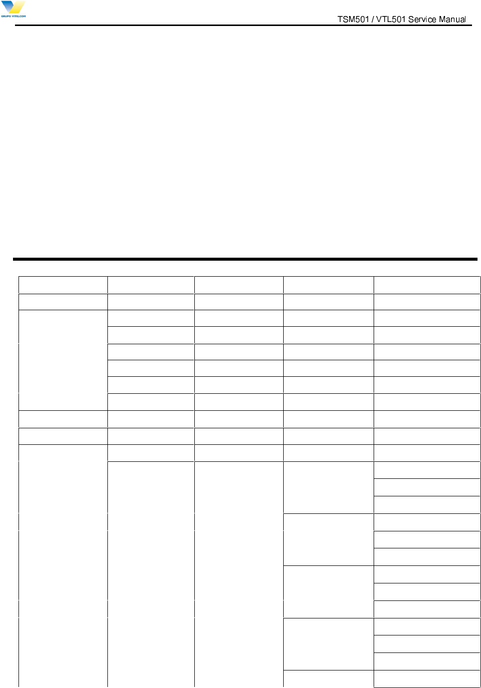
2. Specification
This chapter provides the product configuration and product specifications of TSM501 / VTL501 model,
which operates on Single mode Digital CDMA Telephone and accessories
2.1 Product Structure
[Table 2.1] Standard Package
ITEM TYPES
1 Handheld Portable Telephone TSM501 / VTL501
2 Lithium Ion Battery(850mAh) TSM501 / VTL501
3 AC Charger TSM501 / VTL501 T.C
4 Earphone-Mic Earphone-Mic is offered by VITELCOM
5 Handstrap Handstrap is offered by VITELCOM
6 Owner’s Operating Manual TSM501 / VTL501 Manuals
2.2 TSM501 / VTL501 Specifications
ITEM 800MHz Band
1 Radio Frequency TX: 824 to 849MHz
RX:869 to 894MHz
2 Number of Channels 832
3 Duplex Spacing 45MHz
4 Digital Mode
4.1 Channel Spacing 1.23MHz
4.2 Frequency Stability +/-300Hz
4.3 RF Output Power 24dBm
9LWHOFRP0RELOH7HFKQRORJ\6$ 3URSULHWDU\DQG&RQILGHQWLDO - 5 -
V
V
I
I
T
T
E
E
L
L
C
C
O
O
M
M
M
M
O
O
B
B
I
I
L
L
E
E
T
T
E
E
C
C
H
H
N
N
O
O
L
L
O
O
G
G
Y
Y
S
S
.
.
A
A
.
.
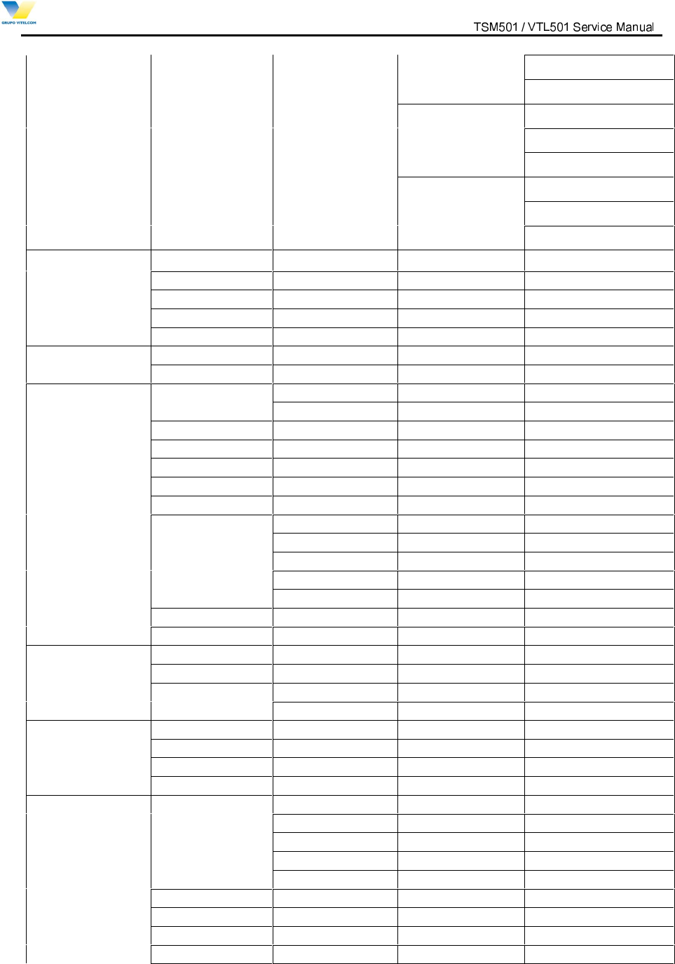
4.4 Receiver Sensitivity -104dBm
4.5 Modulation/Demodulation OQPSK/QPSK
5 Operating Temperature -20 to +60 degrees
6 Power Source Lithium Ion Battery 3.7V, 850mAh
7 Dimensions 50 x 91 x 22.1 mm
(with Standard battery)
8 Weight 89 g (with Standard battery)
Power management
Talk Time(Up to) 147 ~ 156 min(standard battery)
9
Standby(Up to) 120h (standard battery)
Two-way Short Message Service(SMS)
Bell/ Vibration/ LED Alert
10 Features
Multilingual
(Portuguese/English/Spanish)
11 Protocol CDMA 1X
2.3 Battery Specifications
ITEM TYPES
1 Battery Type Lithium Ion Battery
2 Battery Voltage 3.7V
3 Battery Capacity 850mAh
4 Recharging Time With Charger 160 min MAX. at 850mAh Li-ion Battery
2.4 AC Charger Specifications
ITEM TYPES
1 Input Voltage AC 100 ~ 240V (50 / 60Hz)
2 Output Voltage DC 4.2V
3 Output Current 650 mA
9LWHOFRP0RELOH7HFKQRORJ\6$ 3URSULHWDU\DQG&RQILGHQWLDO - 6 -
V
V
I
I
T
T
E
E
L
L
C
C
O
O
M
M
M
M
O
O
B
B
I
I
L
L
E
E
T
T
E
E
C
C
H
H
N
N
O
O
L
L
O
O
G
G
Y
Y
S
S
.
.
A
A
.
.
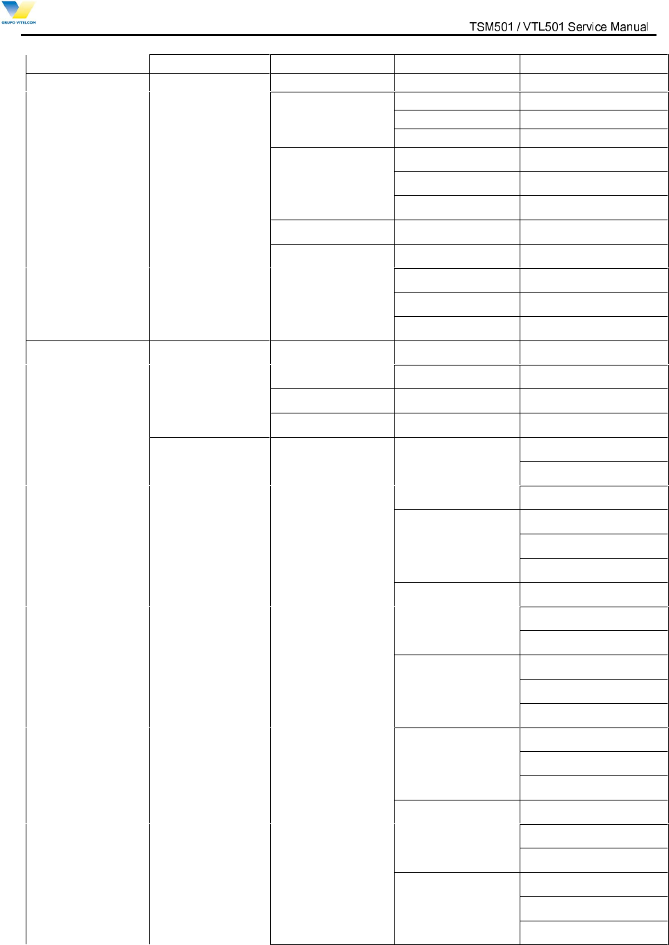
3. Menu Tree
1.Downloads
2.WAP
3.Foto Torpedo 1. Compose
2. Notifications
3. Inbox
4. Outbox
5. Draft
6. Template
4.Voice Mail
5.Voice Portal
6.Tones & Images 1.Tones
2.Images 1.Wallpaper 1.Standby 1.Default
2.Photo Album
3.Download
2.Power On 1.Default
2.Photo Album
3.Download
3.Power Off 1.Default
2.Photo Album
3.Download
4.Incoming Call 1.Default
2.Photo Album
3.Download
5.Outgoing Call 1.Default
9LWHOFRP0RELOH7HFKQRORJ\6$ 3URSULHWDU\DQG&RQILGHQWLDO - 7 -
V
V
I
I
T
T
E
E
L
L
C
C
O
O
M
M
M
M
O
O
B
B
I
I
L
L
E
E
T
T
E
E
C
C
H
H
N
N
O
O
L
L
O
O
G
G
Y
Y
S
S
.
.
A
A
.
.
2.Photo Album
3.Download
6.Sending SMS 1.Default
2.Photo Album
3.Download
7.Connect Internet 1.Default
2.Photo Album
3.Download
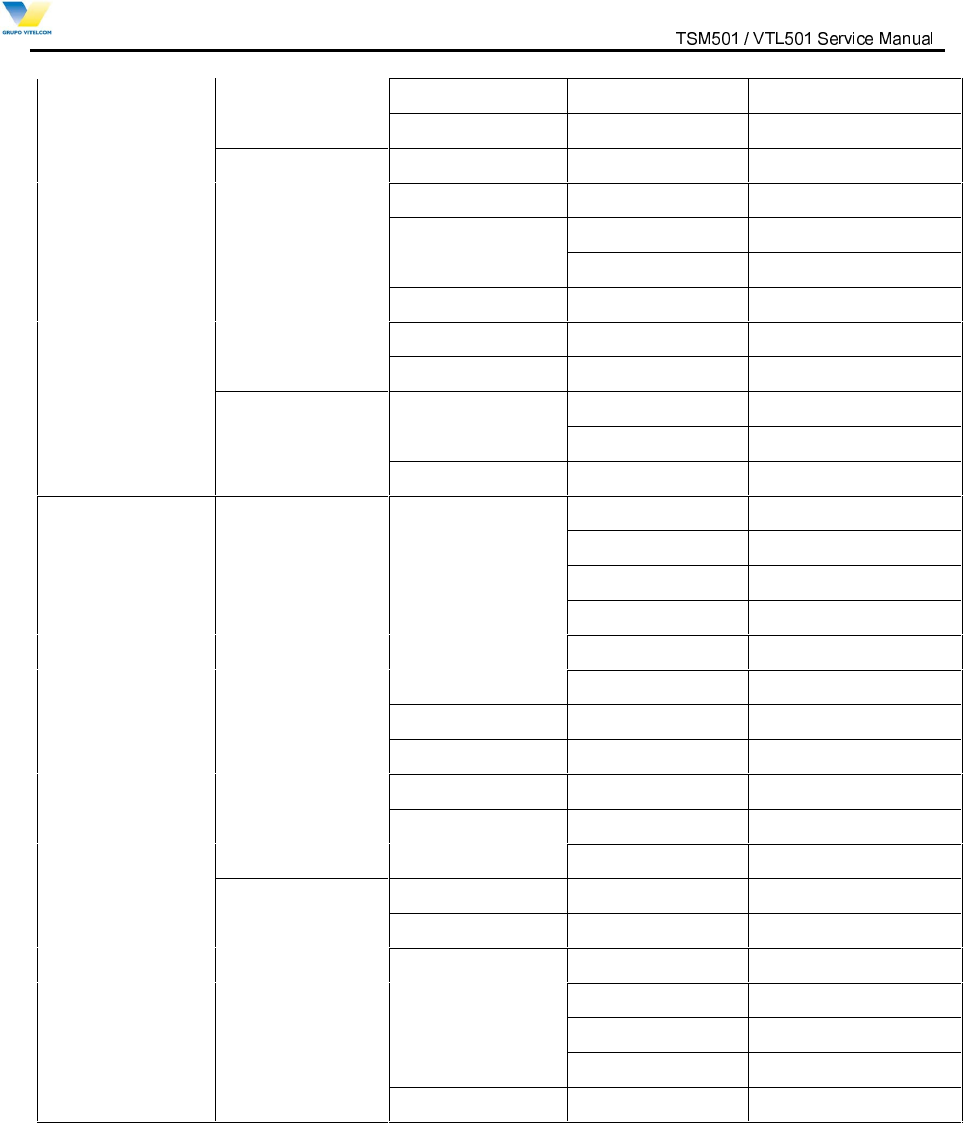
7.Messaging 1.Messenger
2.Chat
3.Torpedo SMS
4.Foto Torpedo
5.E
-
Mail
8.Meu Vivo
1.Reorder menu
2.Initialize menu
9. Torpedo SMS
1
.
Send Message
1.New Message
2.Saved Messages
2.Inbox
3
.Voice Inbox
4
.Outb
ox
5
.Drafts
6.
Delete
7
.Settings
1.Alert Type
2.Alert Tone
3.Show Message
4.
Delivery ACK
5.Canned MSG
8.WAP Alert
9.MMS
10
.Camera
1.Take
Picture
2.Photo Album
3.Set
C
onfig.
1.Save Option
2.Flas
h Option
11.Calls
1.Missed Calls
2.Answered Calls
3.Dial
ed
Calls
4.Call Timers
12
.
Contacts
1.Search Number
1.All
2.By Name
3.By Number
4.By Group
5.By Speedy Dial
2.Add Number
3
.Check Capacity
4
.Delet
e A
ll
5
.Group Edit
9LWHOFRP0RELOH7HFKQRORJ\6$ 3URSULHWDU\DQG&RQILGHQWLDO - 8 -
V
V
I
I
T
T
E
E
L
L
C
C
O
O
M
M
M
M
O
O
B
B
I
I
L
L
E
E
T
T
E
E
C
C
H
H
N
N
O
O
L
L
O
O
G
G
Y
Y
S
S
.
.
A
A
.
.
6
.My Phone No
.
13.Other Functions
1
. Sound
1.Alert Mode
2.Ring/Melody
1.Ring/Melody
2.Ring/VoIce
3.Download
S
ound
3.Ringer Volume 1.Ring Volume
2.Key Volume
3.Hearing Volume
4.Key Tone
5.Call Alert 1.Min. Reminder
2.Connect Alert
3.Discon. Alert
4.SVC Area Alert
5.Power On/Off
6.Lowbatt. Alert
7.Folder Alert
8.DTMF Tone
2.Screen/Lighting 1.Wallpaper 1.Standby 1.Default
2.Photo Album
3.Download
2.Power On 1.Default
2.Photo Album
3.Download
3.Power Off 1.Default
2.Photo Album
3.Download
4.Incoming Call 1.Default
2.Photo Album
3.Download
5.Outgoing Call 1.Default
2.Photo Album
3.Download
6.Sending SMS 1.Default
2.Photo Album
3.Download
7.Connect Internet 1.Default
2.Photo Album
3.Download
9LWHOFRP0RELOH7HFKQRORJ\6$ 3URSULHWDU\DQG&RQILGHQWLDO - 9 -
V
V
I
I
T
T
E
E
L
L
C
C
O
O
M
M
M
M
O
O
B
B
I
I
L
L
E
E
T
T
E
E
C
C
H
H
N
N
O
O
L
L
O
O
G
G
Y
Y
S
S
.
.
A
A
.
.
2.Banner
3. Backlit Ctrl
3.Secretary 1.Moring Call
2.Alarm
3.Schedule 1.Add Schedule
2.View Schedule
4.D-Day
5.Calculator
6.World Time
4.Settings 1.System Menu 1.Select NAM
2.Auto NAM
2.Call Settings 1.Call Waiting
2.CFU
3.CFNA
4.CFB
5.VMNA
6.VMB
7.Auto CSP
3.Answer Mode
4.Language
5.S/W Version
6.Data Service 1.Modem Set-Up
2.Data Speed
5.Security 1.Phone Lock
2.Change Passwd
3.Call Barring 1.Lock Incoming
2.Lock Outgoing
3.Lock Int’l
4.Lock Data SVC
4.Initialize
9LWHOFRP0RELOH7HFKQRORJ\6$ 3URSULHWDU\DQG&RQILGHQWLDO - 10 -
V
V
I
I
T
T
E
E
L
L
C
C
O
O
M
M
M
M
O
O
B
B
I
I
L
L
E
E
T
T
E
E
C
C
H
H
N
N
O
O
L
L
O
O
G
G
Y
Y
S
S
.
.
A
A
.
.
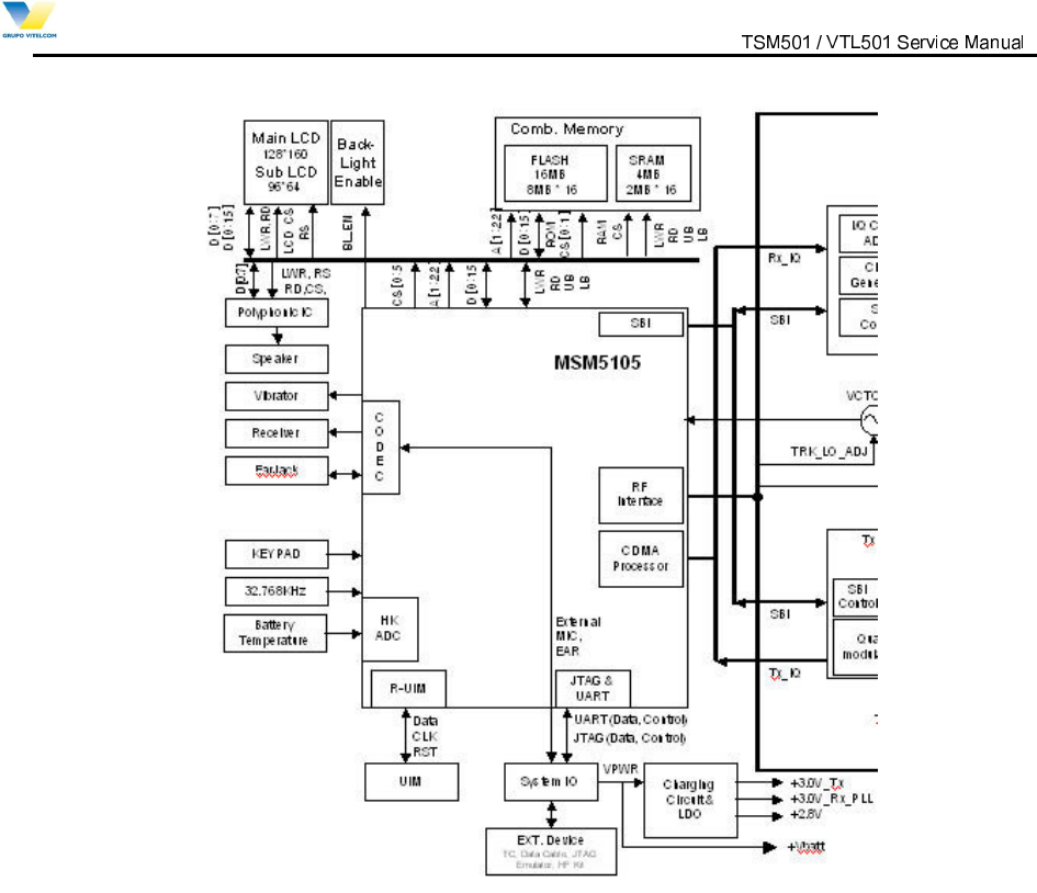
4. Technical Description
4.1 Overview
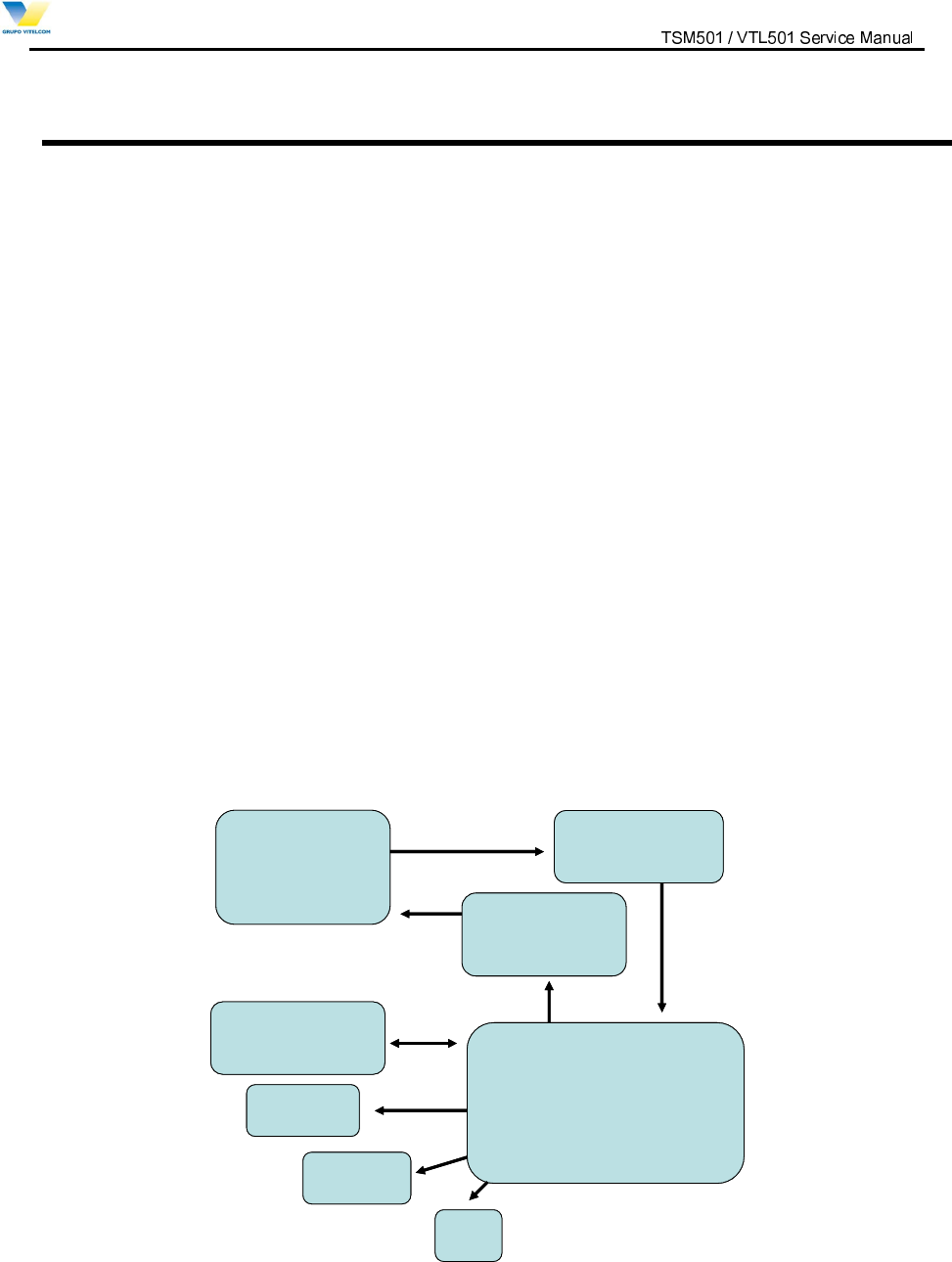
This product consists with 3 parts, which are RF, logic, and UI interface. The block diagram is shown in
Figure 4.1. This product employs the Super-Heterodyne method for wireless communication and the Tx
and Rx frequencies are 824.04~848.97MHz and 869.04~893.9MHz respectively. RF signals received
through the antenna are fed into the low noise amplifier (Receiver MMIC/ LNA, U106) through the duplexer
(F100). Then, they are combined with the signals of local oscillator (VCO, U102) at the down conversion
mixer (Receiver MMIC, U106) in order to create the intermediate frequency (IF). The IF signal is fed into
RX_BBA(U109) through band-pass filter (BPF, U108),. In RX_BBA(U109), the IF signal is changed into
base-band signal. Then, this signal is changed into the digital signal by the analog to digital converter
(ADC, A/D Converter), and the digital circuit part of the MSM(U125) processes the data from ADC. In the
case of transmission, The TX_BBA(U112) receives digital signal from the MSM(U125). In MSM(U125), the
digital signal is changed into analog signal by the digital to analog converter (DAC, D/A Converter), and
then the quadrature signals of base-band are up-converted to the IF frequency bands in TX_BBA(U112).
The Tx AGC in TX_BBA(U112) is designed to be gain-controlled from 85dB dynamic range. In
TX_BBA(U112), the Tx IF frequency mixed with RF local frequency is created Tx RF frequency. After that,
the Power amplifier module(U110) amplifies the RF signal in order to have enough power for radiation.
Finally, the RF signal is sent out to the cell site via the antenna after going through the duplexer (F110).
RF
Sub System
RX_BBA
Baseband-IF
Converter
Memory and UI
Mobile Station Modem
Camera
TX_BBA
Baseband-IF
Converter
LCD
MIDI
RF
Sub System
RX_BBA
Baseband-IF
Converter
Memory and UI
Mobile Station Modem
Camera
TX_BBA
Baseband-IF
Converter
LCD
MIDI
Figure 4.1 Typical Subscriber Unit Block Diagram
9LWHOFRP0RELOH7HFKQRORJ\6$ 3URSULHWDU\DQG&RQILGHQWLDO - 11 -
V
V
I
I
T
T
E
E
L
L
C
C
O
O
M
M
M
M
O
O
B
B
I
I
L
L
E
E
T
T
E
E
C
C
H
H
N
N
O
O
L
L
O
O
G
G
Y
Y
S
S
.
.
A
A
.
.
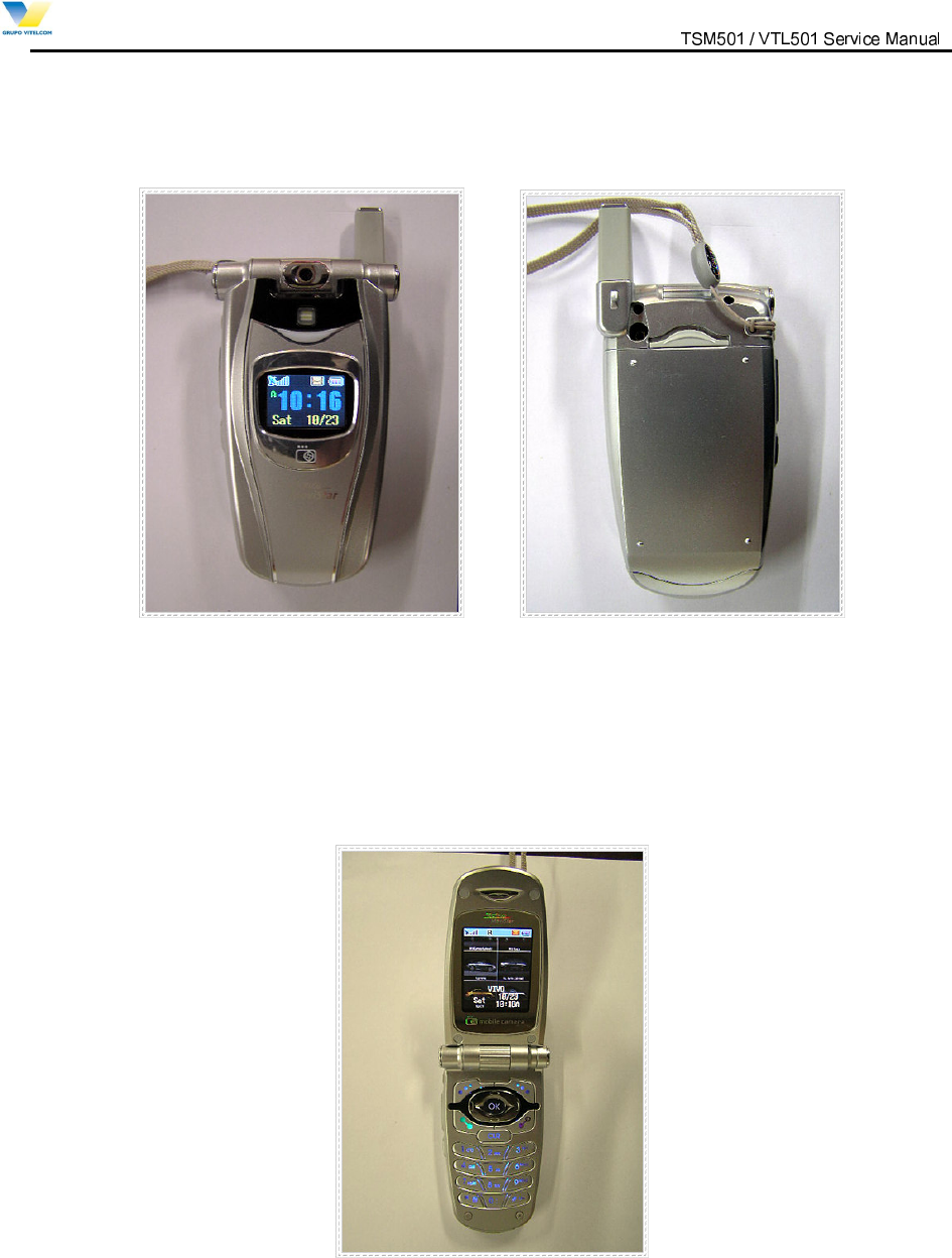
(a)Top view
(b) Bottom View
Figure 4.5 TSM501 / VTL501 External View

9LWHOFRP0RELOH7HFKQRORJ\6$ 3URSULHWDU\DQG&RQILGHQWLDO - 12 -
V
V
I
I
T
T
E
E
L
L
C
C
O
O
M
M
M
M
O
O
B
B
I
I
L
L
E
E
T
T
E
E
C
C
H
H
N
N
O
O
L
L
O
O
G
G
Y
Y
S
S
.
.
A
A
.
.
4.2 RF part Description
The RF part consists of power part, synthesizing part, transmission and reception part.
4.2.1 Description of Frequency Synthesizer Circuit
The UHF band frequency synthesizer is composed of an indirect frequency synthesizer, Phase Locked
Loop (PLL IC, U2), VCO(U102) with the center frequency of 966.88MHz for CDMA mode and Loop Filter.
PLL IC(U2)’s phase detector compares the reference clock frequency (19.68MHz, TCXO(U104) clock)
divided down to 30kHz by the reference divider with a signal divided by the PLL IC(U2) main divider from
the VCO(U102), and generates a local oscillation signals with zero phase difference. These local oscillation
signals are used for Tx and Rx. The other PLL synthesizer controls Tx IF frequency and is implemented on
the TX_BBA(U112). The Tx phase detector receives Tx IF local oscillation signal(260.76MHz) within the
TX_BBA(U112). In Rx IF synthesizer, UHF PLL synthesizer support dual frequencies. Thus
RX_BBA(U109) use UHF PLL to generate the Rx IF frequency(170.76MHz).
Voltage Control Temperature Compensation Crystal Oscillator (VCTCXO, U104)
The temperature variation of reference frequency in a mobile phone can be compensated by
VCTCXO(U104). The reference frequency of a mobile phone is operated stably from –30 to +60 °C. The
VCTCXO(U104) receives frequency tuning signals called TRK_LO_ADJ from MSM(U125) through low-
pass filter in order to generate the reference frequency of 19.68MHz and is used for system main clock.
Frequency stability depending on temperature is within ±1.5 ppm.
RF Frequency Synthesizer
The RF PLL is consisted of the dual mode PLL IC(U2), loop filter, VCO(U102) and VCTCXO(U104). It
generates the RF local frequency of 954.38 ~ 979.38 MHz.
RX IF Frequency Synthesizer
The Rx IF PLL is consisted of the dual mode PLL IC(U2), Rx IF VCO included in the RX_BBA(U109),
loop filter and VCTCXO(U104). The Rx IF VCO included in the RX_BBA(U109) oscillates twice Rx IF
frequency as 170.76MHz and then generates the RX IF frequency of 85.38MHz by dividing the Rx IF
VCO output frequency by two.
TX IF Frequency Synthesizer
The Tx IF PLL Loop is consisted of the Tx IF PLL synthesizer, VCO(U108) that are internally installed in
the TX_BBA(U112), loop filter and VCTCXO(U104). The Tx IF VCO included the TX_BBA(U112)
generates Tx IF local frequency of 260.76MHz and then generates the Tx IF frequency of 130.38MH by

9LWHOFRP0RELOH7HFKQRORJ\6$ 3URSULHWDU\DQG&RQILGHQWLDO - 13 -
V
V
I
I
T
T
E
E
L
L
C
C
O
O
M
M
M
M
O
O
B
B
I
I
L
L
E
E
T
T
E
E
C
C
H
H
N
N
O
O
L
L
O
O
G
G
Y
Y
S
S
.
.
A
A
.
.
dividing the Tx IF VCO output frequency by two.
4.2.2 Description of Rx Part Circuit
Cellular Receiver covers the RF frequency band of 869 ~ 894 MHz and the IF frequency of 85.38MHz.
The RF signal received is sent out to the Receiver MMIC/ LNA(U106) via a duplexer(F100) for
amplification and then, is sent out to the Receiver MMIC/ Down mixer(U106) through Rx RF SAW
filter(U107). Here, the RF signal is mixed with the VCO(U102) signal of 954.38 MHz ~979.38 MHz. IF
signal converted by the Receiver MMIC/ Down mixer(U106) are sent out to IF SAW Filter(U108), which
have a role to filter a wanted frequency. The signal that has passed the IF SAW filter(U108) is fed into
AGC AMP that is controlled by the power density modulation (PDM) signal of the MSM(U125) based on
the strength of received signal. This AGC AMP is tuned into the level corresponding to the input window of
the base band analog processor (RX_BBA, U109). The AGC AMP controls Rx power level within 85dB
dynamic range. The signal entered to RX_BBA(U109) is converted again to 1.2288 MHz base band signal.
To do second frequency conversion, the frequency synthesizer in RX_BBA (U109) generates frequency of
170.76MHz and these signals are divided by two in order to use the Rx IF LO signal. These signals are
used to convert RX IF signals to I/Q base band signal. I and Q base-band signals are respectively sent out
to the analog digital converter via a low pass filter.
Duplexer (F100)
The duplexer(F100) consists of the Rx bandpass filter (BPF) and the Tx BPF which have the function of
separating Tx and Rx signals in the full duplex system for using the common antenna. The Tx BPF is used
to suppress noises and spurious out of the Tx frequency band. The Rx BPF is used to receive only Rx
signal coming from the antenna, which is usually called preselector. Its main function limits the bandwidth
of spectrum reaching the Receiver MMIC/ LNA(U106) and attenuates receiver spurious response. As a
result, the frequency sensitivity and selectivity of mobile phone increase.
Receiver MMIC/ LNA (U106)/ Down Mixer (U106)
- LNA : The characteristics of Low Noise Amplifier (LNA, U106) are low noise figure, high gain, high
intercept point and high reverse isolation. The frequency selectivity characteristic of mobile phone is
mostly determined by LNA(U106).
- The Down Mixer(U106) performs frequency translation by multiplying two signals. The
downconversion mixer employed in the Rx path has two distinctly different inputs, which are RF and
Local Oscillator (LO) signal. The RF signal is downconverted to IF signal by the local oscillator.
Rx RF SAW Filter (U107)
The main function of Rx RF SAW filter(U107) is to attenuate mobile phone spurious frequency, attenuate
direct IF frequency pick up, attenuate noise at the image frequency originating in or amplified by the
LNA(U106) and suppress second harmonic originated in the LNA(U106). The Rx RF SAW filter(U107) is
usually called image filter.
9LWHOFRP0RELOH7HFKQRORJ\6$ 3URSULHWDU\DQG&RQILGHQWLDO - 14 -
V
V
I
I
T
T
E
E
L
L
C
C
O
O
M
M
M
M
O
O
B
B
I
I
L
L
E
E
T
T
E
E
C
C
H
H
N
N
O
O
L
L
O
O
G
G
Y
Y
S
S
.
.
A
A
.
.
Rx IF SAWFilter (U108)
The Rx IF SAW filter(U108) protects its following stages from close-in Inter Modulation (IM) signals,
provides adjacent channel selectivity, and attenuates the second image.
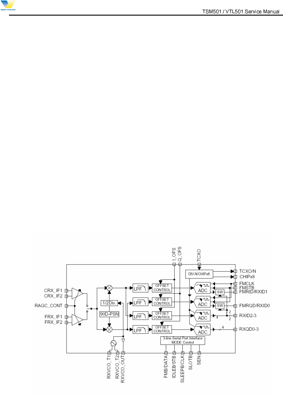
RX_BBA (U109)
Rx_BBA is divided three main parts, IF frequency processing, base-band processing, and digital
interface. It is a receiver IC, installed with a Rx AGC, base-band converter, base-band analog filter, and
A-D converter. It can send a digital base-band signal to digital base-band IC.
The circuit functions of the RX_BBA(U109) include Rx Automatic Gain Controller (AGC) with 90dB
dynamic range input, quadrature IF mixers and Analog to Digital Converters (ADC) for converting to
digital base-band. The RX_BBA(U109) includes clock generators that drive the digital processor and the
VCO(U109) which generates the IF LO frequency for base-band down-conversion. The Rx AGC either
amplifies or attenuates the received CDMA IF signal to provide a constant-amplitude signal to the I/Q
down converter. The IF output of the Rx AGC amplifier separates into I-channel and Q-channel base-
band components and down- converted by mixer with quadrature LO. Rx IF LO signals are generated by
the Voltage Controlled Oscillator of Rx IF. Frequency is stabilized by external varactor-tuned resonant
tank circuit. The I/Q down converter outputs the CDMA signals at base-band frequency. Low-pass
filtering enables the receiver to select the desired base-band signals from the effects of unwanted noise
or adjacent-channel interference. I/Q base band components are converted to digital signals by two
identical 4-bit ADCs. The Block Diagram of the RX_BBA(U109) is shown in Figure 4.6.
Figure 4.6 RX_BBA Functional Block Diagram

9LWHOFRP0RELOH7HFKQRORJ\6$ 3URSULHWDU\DQG&RQILGHQWLDO - 15 -
V
V
I
I
T
T
E
E
L
L
C
C
O
O
M
M
M
M
O
O
B
B
I
I
L
L
E
E
T
T
E
E
C
C
H
H
N
N
O
O
L
L
O
O
G
G
Y
Y
S
S
.
.
A
A
.
.
4.2.3 Description of Tx Part Circuit
The 8 bit digital signal fed into TX_BBA(U112) passes through DAC using TXCLK and TXCLK/ as
triggers to produce base band I/Q signal. Inside the MSM(U125), each signal is sent out to the up mixer via
a digital low pass filter. At the mixer, 130.38 MHz I/Q signal obtained by dividing the 260.76MHz VCO
signal by half is used as carrier for the up-conversion of base band signal to Tx IF signal. This signal is
again up-converted into Tx RF frequency signal. The signal converted into Tx RF frequency is amplified at
the drive amplifier. At the Tx AGC AMP, this Tx IF signal level is varied according to the several
parameters defined in mobile station and base station. The proper gain control signal comes out from the
MSM(U125) in the waveform of PDM and rectified to constant DC voltage level by RC low pass filter. The
gain variable range of Tx AGC AMP is 90 dB. The signal is amplified at the power amplifier. Finally, it is
transmitted out to antenna via a duplexer(F100).
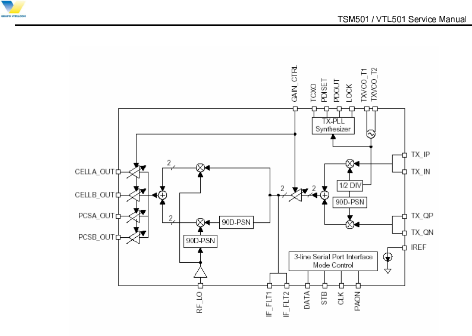
TX_BBA (U112)
The TX_BBA(U112) Base-band-to-RF Transmit Processor including Tx AGC Amplifier, quadrature
mixers, IF synthesized PLL, RF single sideband up converter, RF driver and Tx IF VCO. It converts a base-
band analog signal coming from a digital base-band processor (Modem chip) to an analog RF signal to be
able to Tx PAM.
The TX_BBA(U112) offers the most advanced and integrated CDMA Tx solution along with minimized
power consumption for extended talk-time performance.
The TX_BBA(U112) connects directly with QUALCOMM’s by the MSM(U125) utilizing an analog base-
band interface. The base-band quadrature signals are up-converted to the cellular band and amplified to
provide signal drive capability to the PAM(U110). The TX_BBA(U112) includes an IF frequency, single
sideband up-conversion from IF to RF, two cellular driver amplifiers, and Tx power control through an 85dB
VGA. TX_BBA(U112) functionality is specifically controlled from the MSM(U125) via the three-line serial
bus interface(SBI).
The Block Diagram of the TX_BBA(U112) is shown in Figure 4.7.
Power Amplifier Module (U110)
The power amplifier Module(PAM,U110) that can be used in the CDMA has linear amplification
capability, whereas in the FM mode, it has a high efficiency. For higher efficiency, it is made up of one
MMIC (Monolithic Microwave Integrated Circuit) for which RF input terminal and internal interface circuit
are integrated onto one IC after going through the GaAs HBT (heterojunction bipolar transistor) process.
The PAM(U110) is made up of an output end interface circuit including this MMIC. The RF transmit
signals that have been amplified through the PAM(U110) are sent to the duplexer(F100).
9LWHOFRP0RELOH7HFKQRORJ\6$ 3URSULHWDU\DQG&RQILGHQWLDO - 16 -
V
V
I
I
T
T
E
E
L
L
C
C
O
O
M
M
M
M
O
O
B
B
I
I
L
L
E
E
T
T
E
E
C
C
H
H
N
N
O
O
L
L
O
O
G
G
Y
Y
S
S
.
.
A
A
.
.
Figure 4.7 TX_BBA Functional Block Diagram
4.3 Logic Part Description
The logic part processes the user’s commands and processes all the digital in order to operate in the
phone. The logic part is made up of a keypad/ LCD, receptacle part, voice processing part, mobile station
modem(MSM, U125) part, memory part(U113), and power supply part.
4.3.1 Keypad/ LCD
This is used to transmit keypad signals to MSM(U125).
It is made up of a keypad backlight part that illuminates the keypad, LCD part that displays the operation
status onto the screen, and a receptacle that receives and sends out voice and data with external sources.
4.3.2 Voice Processing Part
The voice processing part is made up of an audio codec and an amplifier used to convert MIC(CON102)
signals into digital voice signals and digital voice signals into analog voice signals.
4.3.3 Mobile Station Modem( MSM, U125)
The MSM(U125) integrates functions that support a CDMA subscriber unit. Subsystems within the
MSM(U125) include a CDMA processor, a QUALCOMM Code Excited Linear Predication (QCELP)
Vocoder, an Enhanced Variable Rate CODEC (EVRC) Vocoder, an ARM7TDMI microprocessor, and
assorted peripheral interfaces that are used to support other functions.

9LWHOFRP0RELOH7HFKQRORJ\6$ 3URSULHWDU\DQG&RQILGHQWLDO - 17 -
V
V
I
I
T
T
E
E
L
L
C
C
O
O
M
M
M
M
O
O
B
B
I
I
L
L
E
E
T
T
E
E
C
C
H
H
N
N
O
O
L
L
O
O
G
G
Y
Y
S
S
.
.
A
A
.
.
MSM(U125) Internal Block
1) ARM Microprocessor Subsystem
The MSM(U125) uses an embedded ARM7TDMI microprocessor. The ARM7TDMI microprocessor,
through the system software, controls most of the functionality for the Mobile Station, including control of
the external peripherals such as the keypad, LCD display, RAM and ROM/FLASH(U113) devices.
2) RF Interface
This block communicates with the MSM(U125) RF, IF and Analog Base-band circuitry.
3) CDMA Subsystem: Digital IS-2000 Signal Processing.
Searcher engine
Demodulating fingers
Combining block
Frame de-interleaver
Viterbi decoder
Reverse link subsystem
4) UART (Universal Asynchronous Receiver Transmitter)
Two identical UARTs, UART1 has dedicated pins while UART2 share multiplexed pins with the Auxiliary
PCM CODEC interface.
5) Vocoder Subsystem
The MSM(U125)’s QDSP2000 supports EVRC and QCELP13K vocoders. In addition, the QDSP2000 has
modules to support the following audio functions; DTMF tone generation, DTMF tone detection, Tx/Rx
volume controls, Tx/Rx automatic gain control(AGC), Rx Automatic Volume Control(AVC), Ear Seal Echo
Canceller(ESEC), Acoustic Echo Canceller(AEC), Noise Suppression(NS), and programmable, 13-tap,
Type-I, FIR, Tx/Rx compensation filters. The MSM(U125)’s integrated ARM7TDMI processor downloads
the firmware into the QDSP2000 and configures QDSP2000 to support the desired functionality.
6) General Purpose Interface Bus
The MSM(U125) has 48 general-purpose bi-directional input/output pins (GPIO_INT[47:0]) that double as
general-purpose interrupt inputs. Some of the GPIO_INT pins have alternate functions supported on them.
The alternate functions include, USB interface, additional RAM, ROM/Flash(U113), general-purpose chip
selects, parallel LCD interface, and a UART interface. The function of these pins is documented in the
various software releases.
7) Serial Bus Interface

9LWHOFRP0RELOH7HFKQRORJ\6$ 3URSULHWDU\DQG&RQILGHQWLDO - 18 -
V
V
I
I
T
T
E
E
L
L
C
C
O
O
M
M
M
M
O
O
B
B
I
I
L
L
E
E
T
T
E
E
C
C
H
H
N
N
O
O
L
L
O
O
G
G
Y
Y
S
S
.
.
A
A
.
.
This interface is specifically designed to be a quick, low pin count control protocol for
Qualcomm’s TX_BBA(U112) can be configured for different operating modes and configured for minimum
power consumption, extending battery life in standby mode.
8) User Interface
MSM(U125) user interface comprises digital connections to the subscriber unit ringer transducer, keypad
and LCD display.
9) Mode Select and JTAG Interfaces
The Mode select inputs to the MSM(U125) determine overall mode of the ASIC. The options under the
control of the Mode select inputs are Native Mode which is the normal subscriber unit operation and ICE
Mode in which the on-chip ARM microprocessor is disabled, allowing off-chip emulation by the ICE unit.
4.3.4 Memory Part (U113)
Components: Combination Memory [Flash Memory (128Mbit) + SRAM (32Mbit)]
1) Flash Memory (128Mbit)
Stores telephone’s main and sub programs.
Memory for source code : 12Mbyte .
Memory for NV parameter value , SMS, Phone Book, Download data, PIMS data, camera data.. etc :
4Mbyte.
- Code Flash memory: 8MB (4Mbit x 16), Random Access Time is 70ns
- Data Flash memory: 8MB (4Mbit x 16), Random Access Time is 70ns
2) SRAM (32Mbit)
Stores changes in other person’s system parameter and Data Task data Buffer and stack of each task.
- SRAM: 4MB (2Mbit x 16), Max. Access Time is 70ns
4.3.5 Power Supply Part
Power is supplied by battery or external source of which range is 3.2~4.2V voltage. It is sent to LDO (Low
dropout regulator), which supply 2.8V for Logic power.
9LWHOFRP0RELOH7HFKQRORJ\6$ 3URSULHWDU\DQG&RQILGHQWLDO - 19 -
V
V
I
I
T
T
E
E
L
L
C
C
O
O
M
M
M
M
O
O
B
B
I
I
L
L
E
E
T
T
E
E
C
C
H
H
N
N
O
O
L
L
O
O
G
G
Y
Y
S
S
.
.
A
A
.
.
Figure 4.8 VTL501 Logic Part Block Diagram
4.4 Power Up Sequence
This section describes the steps how the TSM501 / VTL501 phone wakes up.
Place a Battery Pack
The battery pack, which the protection circuit is implemented, is placed into the phone.
Press and Hold [END] Key
The Power on circuit (SW124) generates the control voltage to be used for U6.
Regulators Activated
U6 feeds 2.8V to MSM (U125), LCD
U6 feeds 2.8V to Flash ROM / SRAM (U113) and others.
U6 feeds 2.8V to VCTCXO(U104) and others.

9LWHOFRP0RELOH7HFKQRORJ\6$ 3URSULHWDU\DQG&RQILGHQWLDO - 20 -
V
V
I
I
T
T
E
E
L
L
C
C
O
O
M
M
M
M
O
O
B
B
I
I
L
L
E
E
T
T
E
E
C
C
H
H
N
N
O
O
L
L
O
O
G
G
Y
Y
S
S
.
.
A
A
.
.
VCTCXO Activated
When the power is fed to the VCTCXO(U104), it generates 19.68MHz to be used for the MPU clock.
Reset Pulses Generated
a) The reset pulse is generated with U6 when it is feed with the power.
b) The reset pulse (RESOUT/) for the MCP is generated with MSM(U125) right after the item a).
c) The reset pulse (RESOUT/) for the LCD is generated with MSM(U125)
MSM(U125) Starts
Based on the reset pulse a), the MSM(U125) starts to operate including accesses to the Flash ROM and
SRAM (U113). The watchdog timer operates repeatedly.
Phone Wakes Up
Under control of the MSM(U125), the phone displays a wake-up animation, turn the backlight on and
sounds a melody.
9LWHOFRP0RELOH7HFKQRORJ\6$ 3URSULHWDU\DQG&RQILGHQWLDO - 21 -
V
V
I
I
T
T
E
E
L
L
C
C
O
O
M
M
M
M
O
O
B
B
I
I
L
L
E
E
T
T
E
E
C
C
H
H
N
N
O
O
L
L
O
O
G
G
Y
Y
S
S
.
.
A
A
.
.
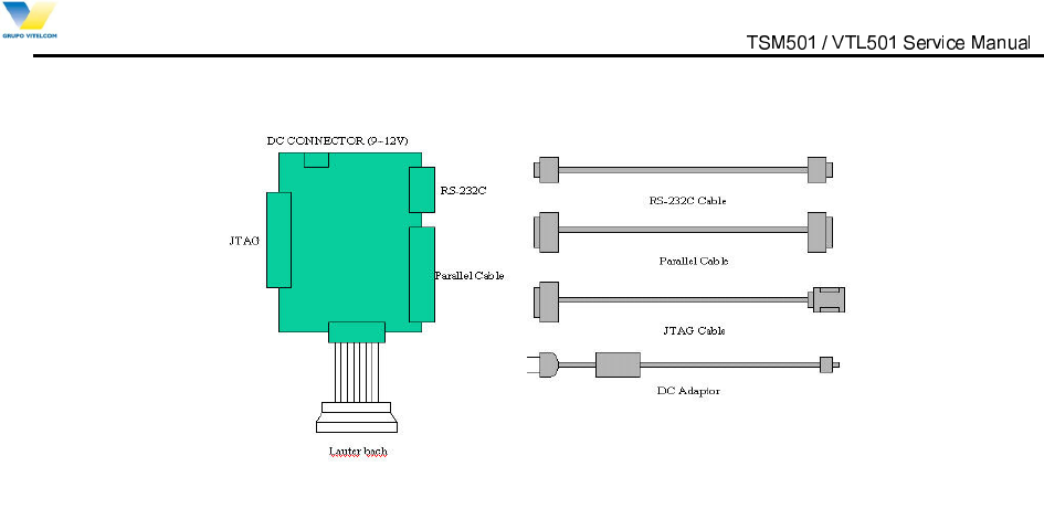
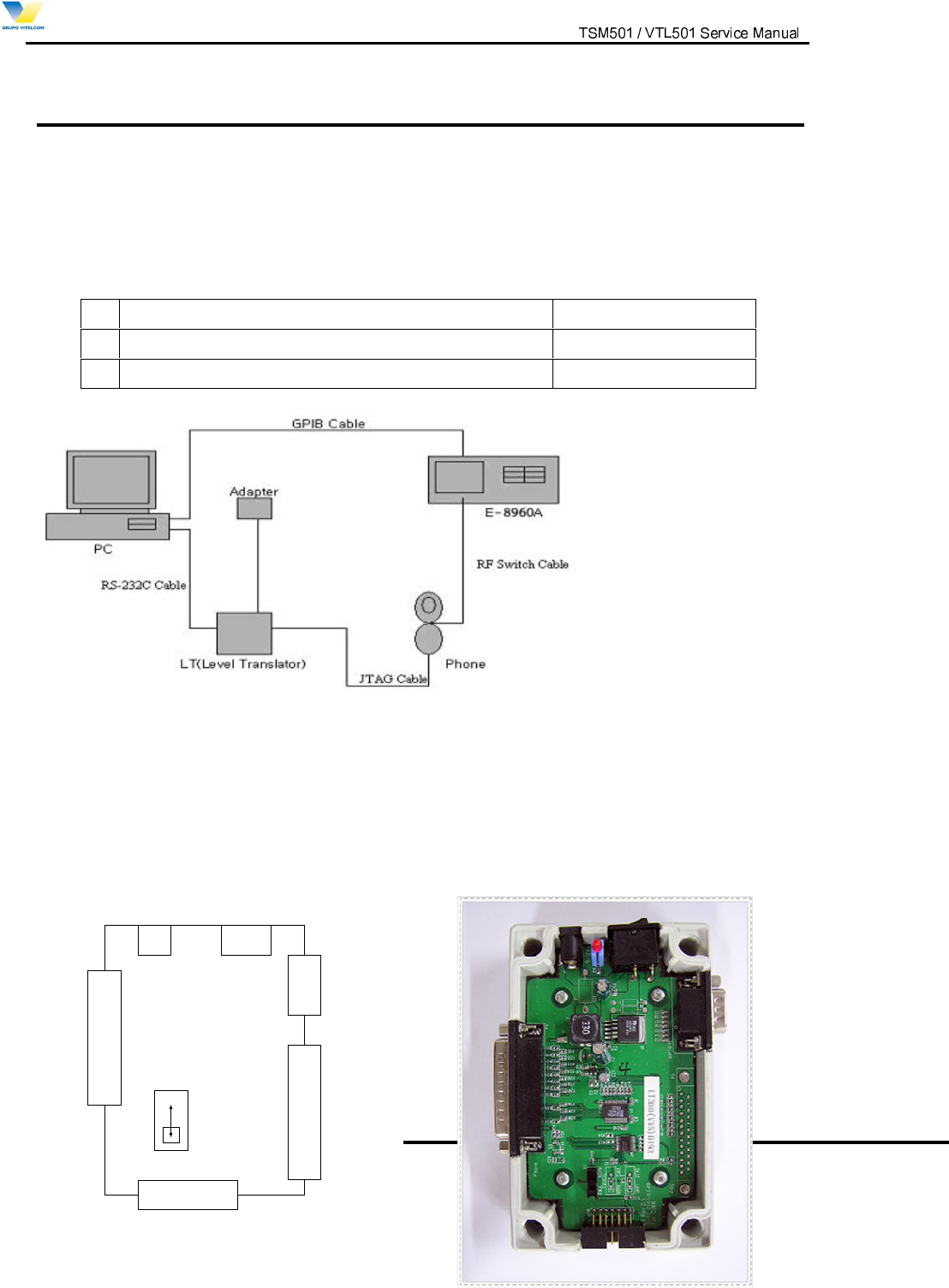
5. Servicing Tools
5.1 SERVICING TOOLS
This chapter provides information for the servicing tools of TSM501 / VTL501 Single mode digital CDMA
Telephone.
TSM501 / VTL501 Service tools
No
Item Description
1 Level Translator Provides the interface between the PC RS-232C data and Phone
Provides the interface between the PC JTAG data and Phone
2 RS-232C Cable Connects the L/T and the PC for RS-232C data Communication
3 Parallel Cable Connects the L/T and the PC for JTAG data Communication
4 JTAG Cable Connects the L/T and Phone
5 DC Adaptor Connects the L/T and the Power supply
6 Lauter-Bach Provides the interface between the PC JTAG data and phone,
It’s used only when the phone’s totally dead, crash, etc.
Series of necessary software
Install below-written programs somewhere in host PC disk
(Caution: make sure to remember the path)
No Item
1 Bin file (Includes most of target programs to operate phone)
2 Script file
(Includes information in connecting phone with base station of Service Provider)
3 Trace 32 (the program used for Lauterbach)
4 Downloader (it is needed in downloading target programs into phone)
5 UI tester (the program used for testing User Interface part)
6 CAL Data Writing
9LWHOFRP0RELOH7HFKQRORJ\6$ 3URSULHWDU\DQG&RQILGHQWLDO - 22 -
V
V
I
I
T
T
E
E
L
L
C
C
O
O
M
M
M
M
O
O
B
B
I
I
L
L
E
E
T
T
E
E
C
C
H
H
N
N
O
O
L
L
O
O
G
G
Y
Y
S
S
.
.
A
A
.
.
Figure 5.1 L T (Level Translator)
9LWHOFRP0RELOH7HFKQRORJ\6$ 3URSULHWDU\DQG&RQILGHQWLDO - 23 -
V
V
I
I
T
T
E
E
L
L
C
C
O
O
M
M
M
M
O
O
B
B
I
I
L
L
E
E
T
T
E
E
C
C
H
H
N
N
O
O
L
L
O
O
G
G
Y
Y
S
S
.
.
A
A
.
.
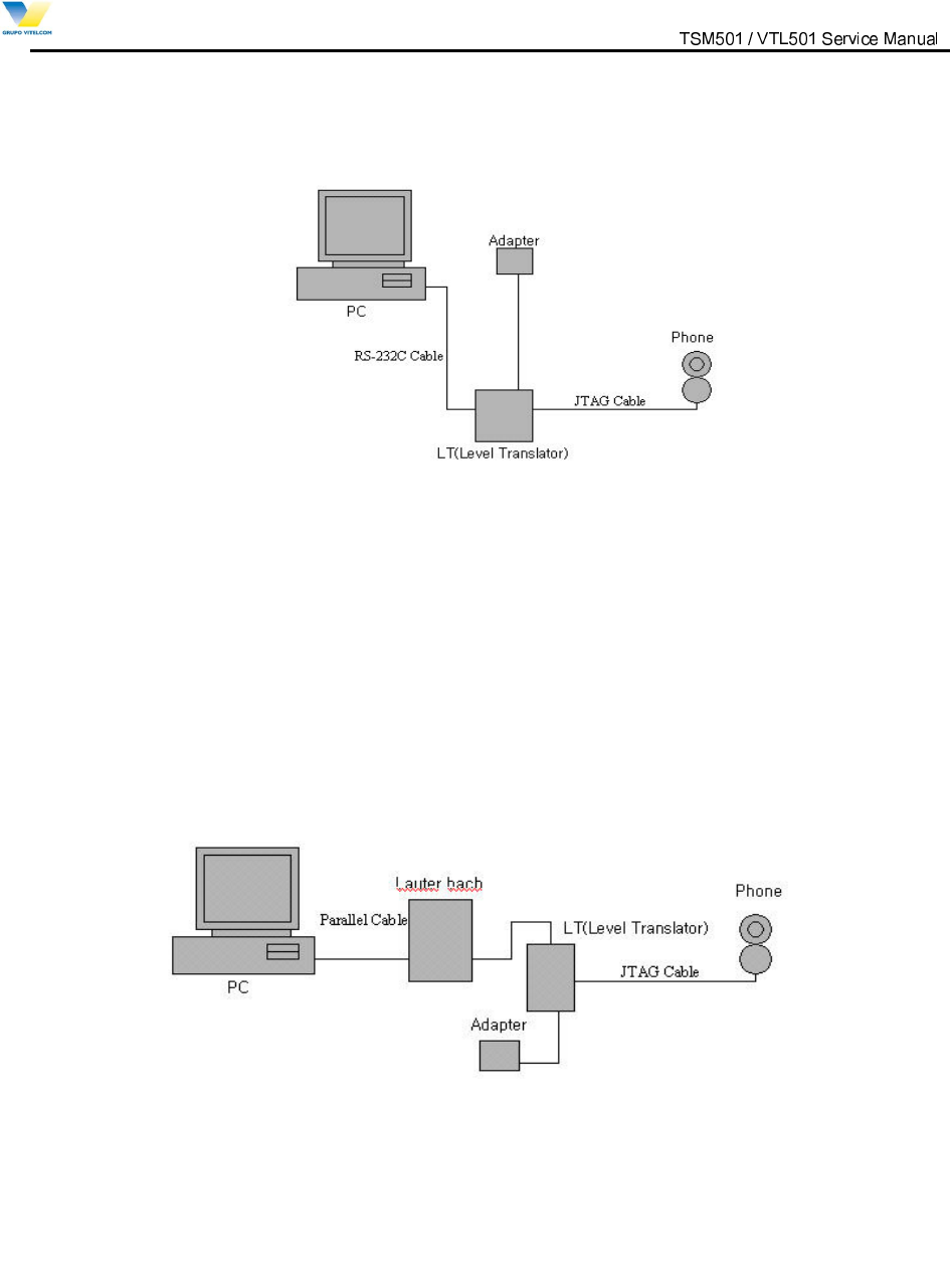
Figure 5.2 Connects the Equipments for Bin & Script Downloading
Figure 5.3 Connects the Equipments for using Lauterbach
9LWHOFRP0RELOH7HFKQRORJ\6$ 3URSULHWDU\DQG&RQILGHQWLDO - 24 -
V
V
I
I
T
T
E
E
L
L
C
C
O
O
M
M
M
M
O
O
B
B
I
I
L
L
E
E
T
T
E
E
C
C
H
H
N
N
O
O
L
L
O
O
G
G
Y
Y
S
S
.
.
A
A
.
.
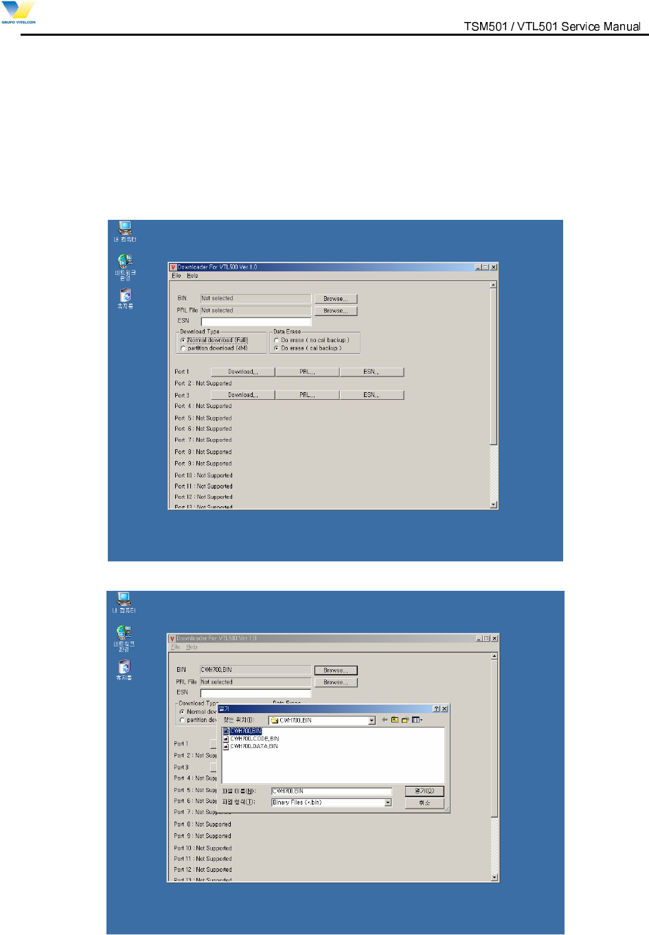
5.2 Downloader
5.2.1 How to download binary file.
1) Run “Downloader_VTL501.exe”.
2) Check “Normal Download(Full)” radio button in “Download Type”.
3) Check “Do Erase( cal backup )” radio button in “Data Erase”.
4) Press “Browse” Button to choose binary file.
9LWHOFRP0RELOH7HFKQRORJ\6$ 3URSULHWDU\DQG&RQILGHQWLDO - 25 -
V
V
I
I
T
T
E
E
L
L
C
C
O
O
M
M
M
M
O
O
B
B
I
I
L
L
E
E
T
T
E
E
C
C
H
H
N
N
O
O
L
L
O
O
G
G
Y
Y
S
S
.
.
A
A
.
.
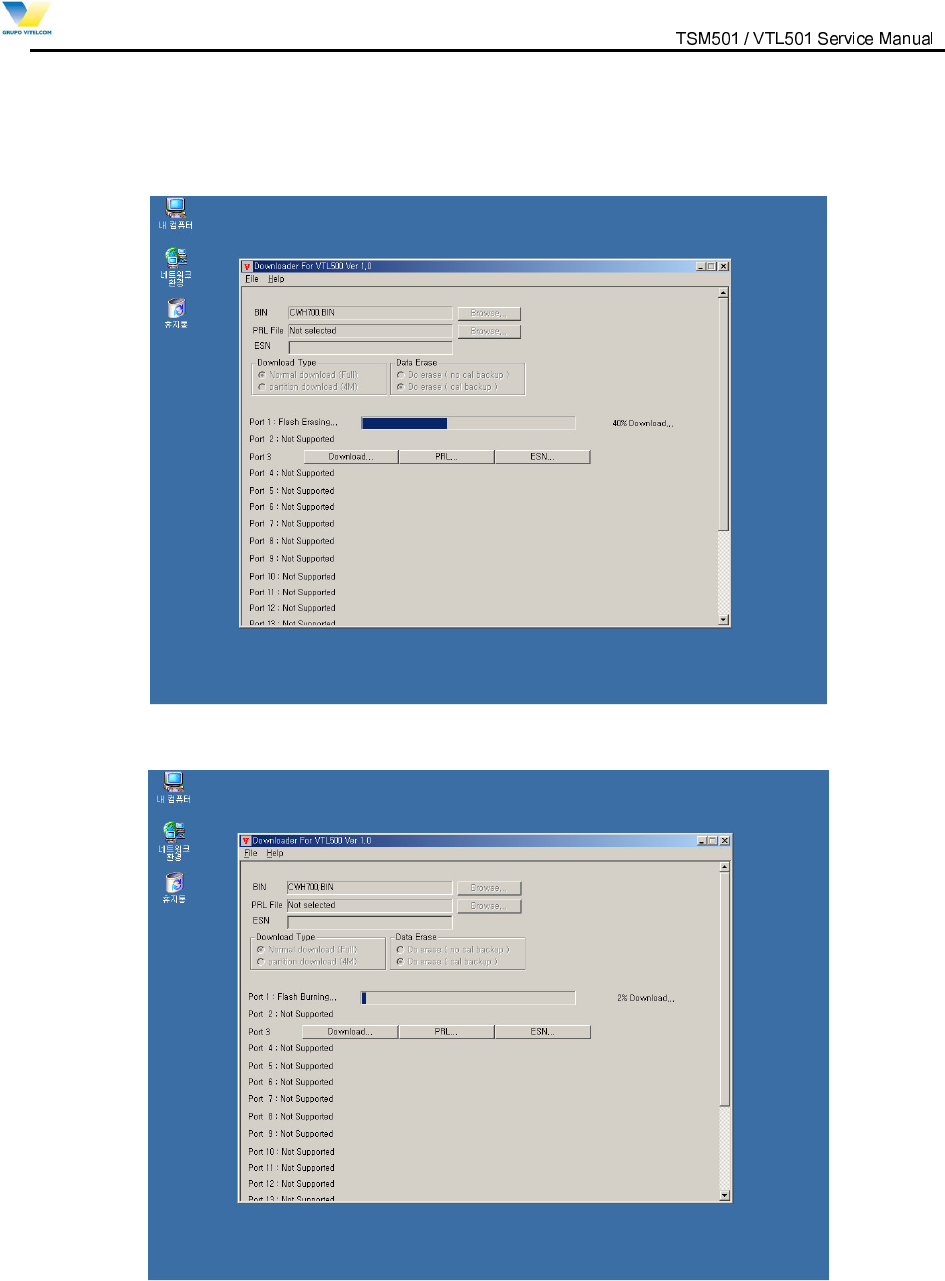
5) Press ”Download…” Button to start downloading binary file.
Downloader erases flash at first.
6) Downloader is burning flash with binary file.
9LWHOFRP0RELOH7HFKQRORJ\6$ 3URSULHWDU\DQG&RQILGHQWLDO - 26 -
V
V
I
I
T
T
E
E
L
L
C
C
O
O
M
M
M
M
O
O
B
B
I
I
L
L
E
E
T
T
E
E
C
C
H
H
N
N
O
O
L
L
O
O
G
G
Y
Y
S
S
.
.
A
A
.
.
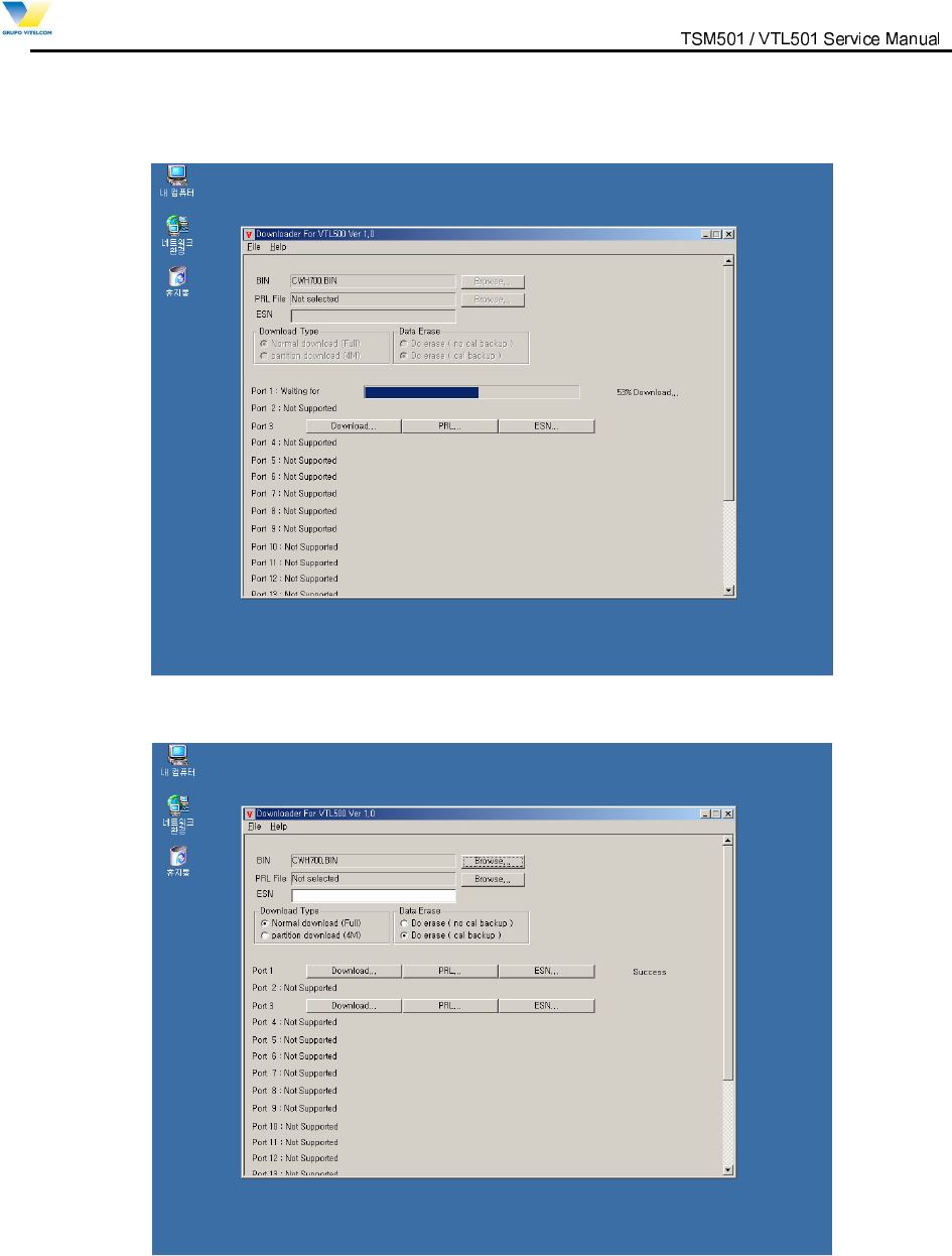
7) Wait until phone boots two times.
8) Downloading binary file is well done if downloader displays “Success”
9LWHOFRP0RELOH7HFKQRORJ\6$ 3URSULHWDU\DQG&RQILGHQWLDO - 27 -
V
V
I
I
T
T
E
E
L
L
C
C
O
O
M
M
M
M
O
O
B
B
I
I
L
L
E
E
T
T
E
E
C
C
H
H
N
N
O
O
L
L
O
O
G
G
Y
Y
S
S
.
.
A
A
.
.
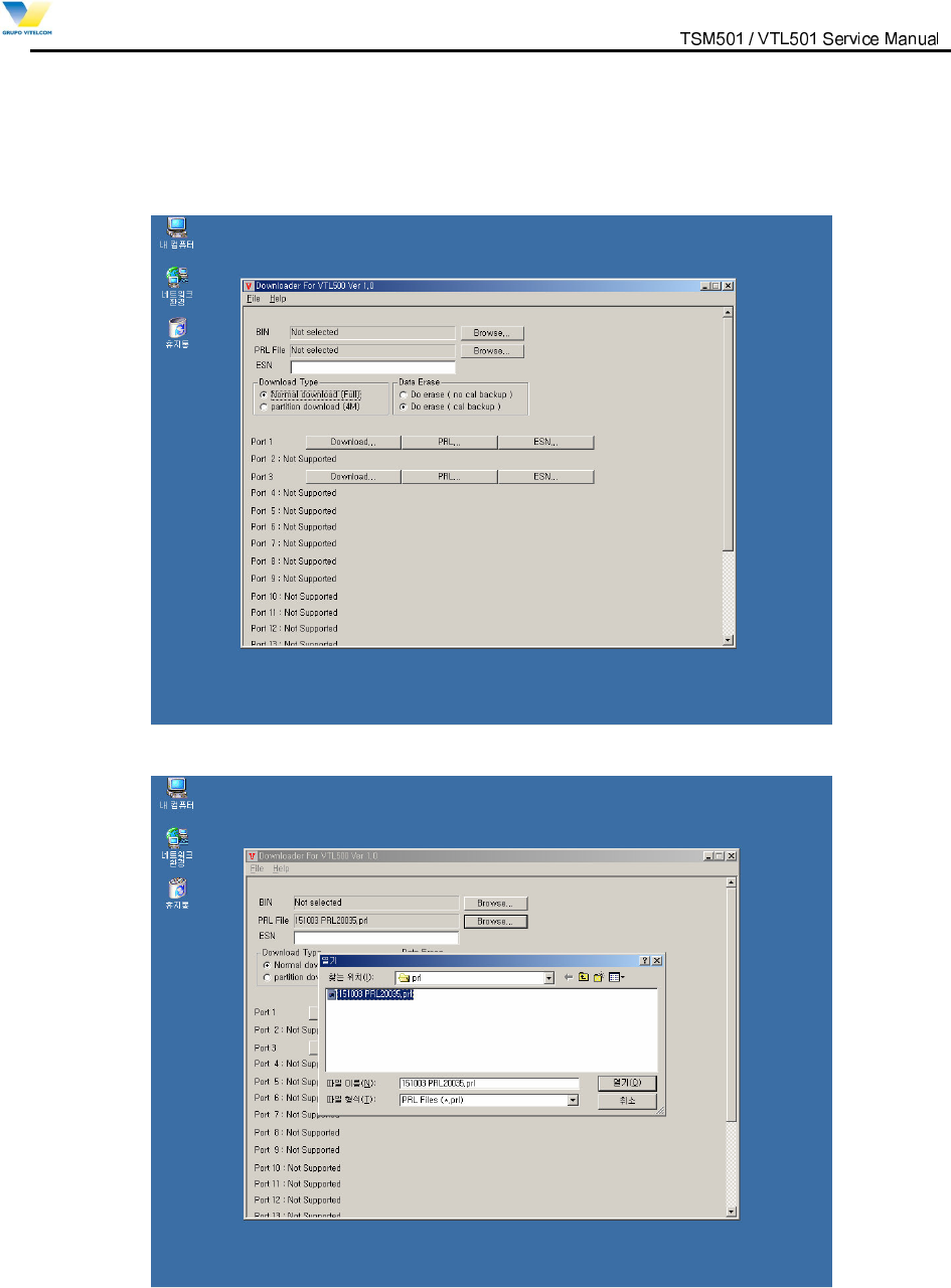
5.2.2 How to change roaming list
1) Run “Downloader_VTL501.exe”.
2) Press “Browse” Button to choose roaming list file.
9LWHOFRP0RELOH7HFKQRORJ\6$ 3URSULHWDU\DQG&RQILGHQWLDO - 28 -
V
V
I
I
T
T
E
E
L
L
C
C
O
O
M
M
M
M
O
O
B
B
I
I
L
L
E
E
T
T
E
E
C
C
H
H
N
N
O
O
L
L
O
O
G
G
Y
Y
S
S
.
.
A
A
.
.
3) Press ”PRL…” Button to start downloading roaming list file.
4) Downloading roaming list file is well done if downloader displays “Success”.
9LWHOFRP0RELOH7HFKQRORJ\6$ 3URSULHWDU\DQG&RQILGHQWLDO - 29 -
V
V
I
I
T
T
E
E
L
L
C
C
O
O
M
M
M
M
O
O
B
B
I
I
L
L
E
E
T
T
E
E
C
C
H
H
N
N
O
O
L
L
O
O
G
G
Y
Y
S
S
.
.
A
A
.
.
5.2.3 How to write ESN
1) Run “Downloader_VTL501.exe”.
2) Write ESN in Edit Box in hexadecimal.
9LWHOFRP0RELOH7HFKQRORJ\6$ 3URSULHWDU\DQG&RQILGHQWLDO - 30 -
V
V
I
I
T
T
E
E
L
L
C
C
O
O
M
M
M
M
O
O
B
B
I
I
L
L
E
E
T
T
E
E
C
C
H
H
N
N
O
O
L
L
O
O
G
G
Y
Y
S
S
.
.
A
A
.
.
3) Press ”ESN…” Button to write ESN to phone.
4) Writing ESN is well done if downloader displays “Success”.
9LWHOFRP0RELOH7HFKQRORJ\6$ 3URSULHWDU\DQG&RQILGHQWLDO - 31 -
V
V
I
I
T
T
E
E
L
L
C
C
O
O
M
M
M
M
O
O
B
B
I
I
L
L
E
E
T
T
E
E
C
C
H
H
N
N
O
O
L
L
O
O
G
G
Y
Y
S
S
.
.
A
A
.
.
5.3 HOW TO USE LAUTERBACH
Lauterbach is only used when the phone is completely dead and needs recovering,
In advance, connect all equipments following the picture “FIG 5.3”. First
And then follow the next steps.
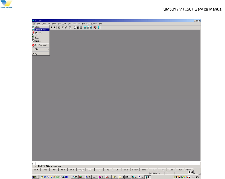
1st PROCESS : TRACE32
1. Execute the “ Trace 32” software in order to operate Lauterbach
INITIAL DISPLAY.
FIG 5.4 INITIAL DISPLAY of TRACE 32
1. CLICK “FILE->OPEN BATCHFILE. (Figure 5.5)” on the tool bar
9LWHOFRP0RELOH7HFKQRORJ\6$ 3URSULHWDU\DQG&RQILGHQWLDO - 32 -
V
V
I
I
T
T
E
E
L
L
C
C
O
O
M
M
M
M
O
O
B
B
I
I
L
L
E
E
T
T
E
E
C
C
H
H
N
N
O
O
L
L
O
O
G
G
Y
Y
S
S
.
.
A
A
.
.
Figure 5.5
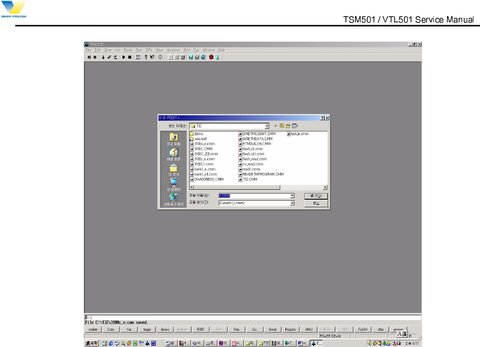
2. Click the demanded file on window.
-Find and click the proper file ( *.cmm) shown on the window of Fig 5.6.
9LWHOFRP0RELOH7HFKQRORJ\6$ 3URSULHWDU\DQG&RQILGHQWLDO - 33 -
V
V
I
I
T
T
E
E
L
L
C
C
O
O
M
M
M
M
O
O
B
B
I
I
L
L
E
E
T
T
E
E
C
C
H
H
N
N
O
O
L
L
O
O
G
G
Y
Y
S
S
.
.
A
A
.
.
Figure 5.6
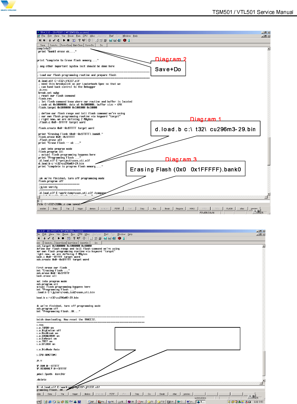
3. Set ‘BIN FILE’ Route for downloading (Figure 4.7)
-. Replace the path of Diagram 1 with that of where BIN file is located on PC now.
-. Click “ Save+Do”(Diagram 2) & pwr key on handset” at the same time for about 5 sec until
“ Erasing Flash( 0x0--0xBFFFFF).bank (Diagram 3)” shows up.
9LWHOFRP0RELOH7HFKQRORJ\6$ 3URSULHWDU\DQG&RQILGHQWLDO - 34 -
V
V
I
I
T
T
E
E
L
L
C
C
O
O
M
M
M
M
O
O
B
B
I
I
L
L
E
E
T
T
E
E
C
C
H
H
N
N
O
O
L
L
O
O
G
G
Y
Y
S
S
.
.
A
A
.
.
—
Figure 5.7
'LDJUDP
“
3URJUDPPLQJ)ODVK2.”
Figure 5.8
9LWHOFRP0RELOH7HFKQRORJ\6$ 3URSULHWDU\DQG&RQILGHQWLDO - 35 -
V
V
I
I
T
T
E
E
L
L
C
C
O
O
M
M
M
M
O
O
B
B
I
I
L
L
E
E
T
T
E
E
C
C
H
H
N
N
O
O
L
L
O
O
G
G
Y
Y
S
S
.
.
A
A
.
.
When "Programming Flash..OK...” show, the whole downloading procedure is completed. (Figure 5.8)
4. Power off/on Level Translator
2nd PROCESS : CAL Data Writing
- SEE “ 5.5 CAL. DATA WRITING”
3rd PROCESS : NEW_ DOWNLOADER.EXE ( Downloading script file )
- SEE “ 5.2 NEW DOWNLOADER”
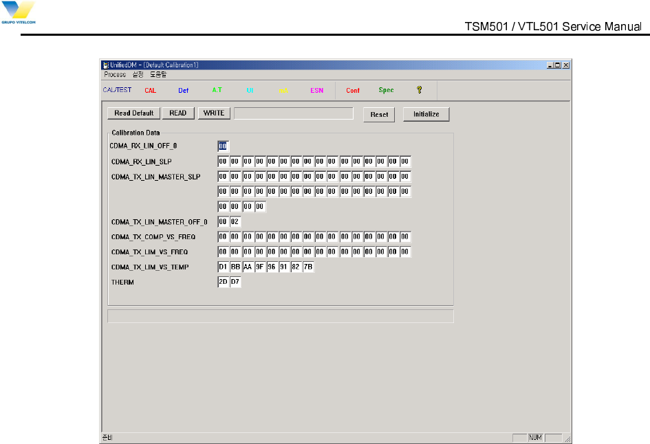
5.4 CAL.exe (writing CAL Data)
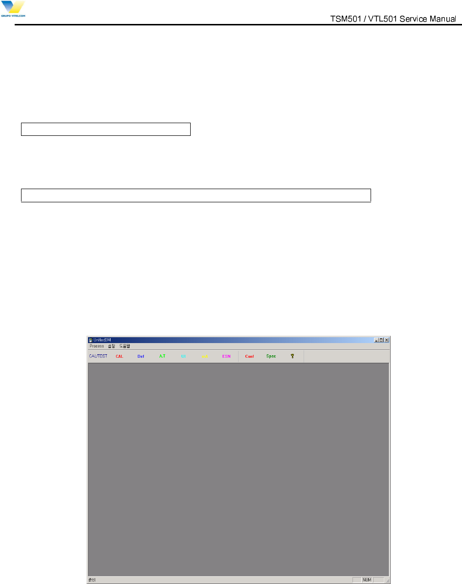
1) Connect all equipments following FIG 5.3 and then execute “UnifiedDM” software. Press
INITIAL DISPLAY
2) Select “Def”, and slect “Initialize” menu
- Readed Cal data will be loaded
9LWHOFRP0RELOH7HFKQRORJ\6$ 3URSULHWDU\DQG&RQILGHQWLDO - 36 -
V
V
I
I
T
T
E
E
L
L
C
C
O
O
M
M
M
M
O
O
B
B
I
I
L
L
E
E
T
T
E
E
C
C
H
H
N
N
O
O
L
L
O
O
G
G
Y
Y
S
S
.
.
A
A
.
.
3) Click the “ Write” button
- When “Success” display, the procedure of writing Cal _Data is all completed.
4) Reboot phone (Power Off/On ).
- When “Success” display, the procedure of writing Cal _Data is all completed.
5HERRWSKRQH3RZHU2II2Q
9LWHOFRP0RELOH7HFKQRORJ\6$ 3URSULHWDU\DQG&RQILGHQWLDO - 37 -
V
V
I
I
T
T
E
E
L
L
C
C
O
O
M
M
M
M
O
O
B
B
I
I
L
L
E
E
T
T
E
E
C
C
H
H
N
N
O
O
L
L
O
O
G
G
Y
Y
S
S
.
.
A
A
.
.
6. MEASUREMENT
6.1 Measurement Configuration
Measurement tool
TSM510 / VTL501 Service tools + RF Switch Cable
Insertion Loss of RF Switch Cable
No
Item Typical Loss
1 RF Switch Cable insertion loss at 800MHz band 1.0 dB
2 RF Switch Cable insertion loss at 1900MHz band 1.0 dB
Figure 6.1 Configuration for Adjustment and Test of Cellular Phone
1. Lauter bach Mode : select Emul in S1
-7$*0RGHVHOHFW1RUPLQ6
)LJXUH&RQILJXUDWLRQRI/HYHO7UDQVODWRU
JTAG
Lauter Bach
DC Connector
(9~12V)
RS-232C
Parallel
Cable
S1
(Dip Switch)
Norm
Em ul
Power
Switch