Volansys Technologies pvt MKW41Z VT-MKW41Z User Manual Proposal
Volansys Technologies pvt ltd VT-MKW41Z Proposal
Users Manual
VT-MKW41Z Module Datasheet
Rev 0.4 Confidential Copyright © 2017 Volansys
Volansys Technologies Page | 1
BLUETOOTH® LOW ENERGY,
IEEE® 802.15.4
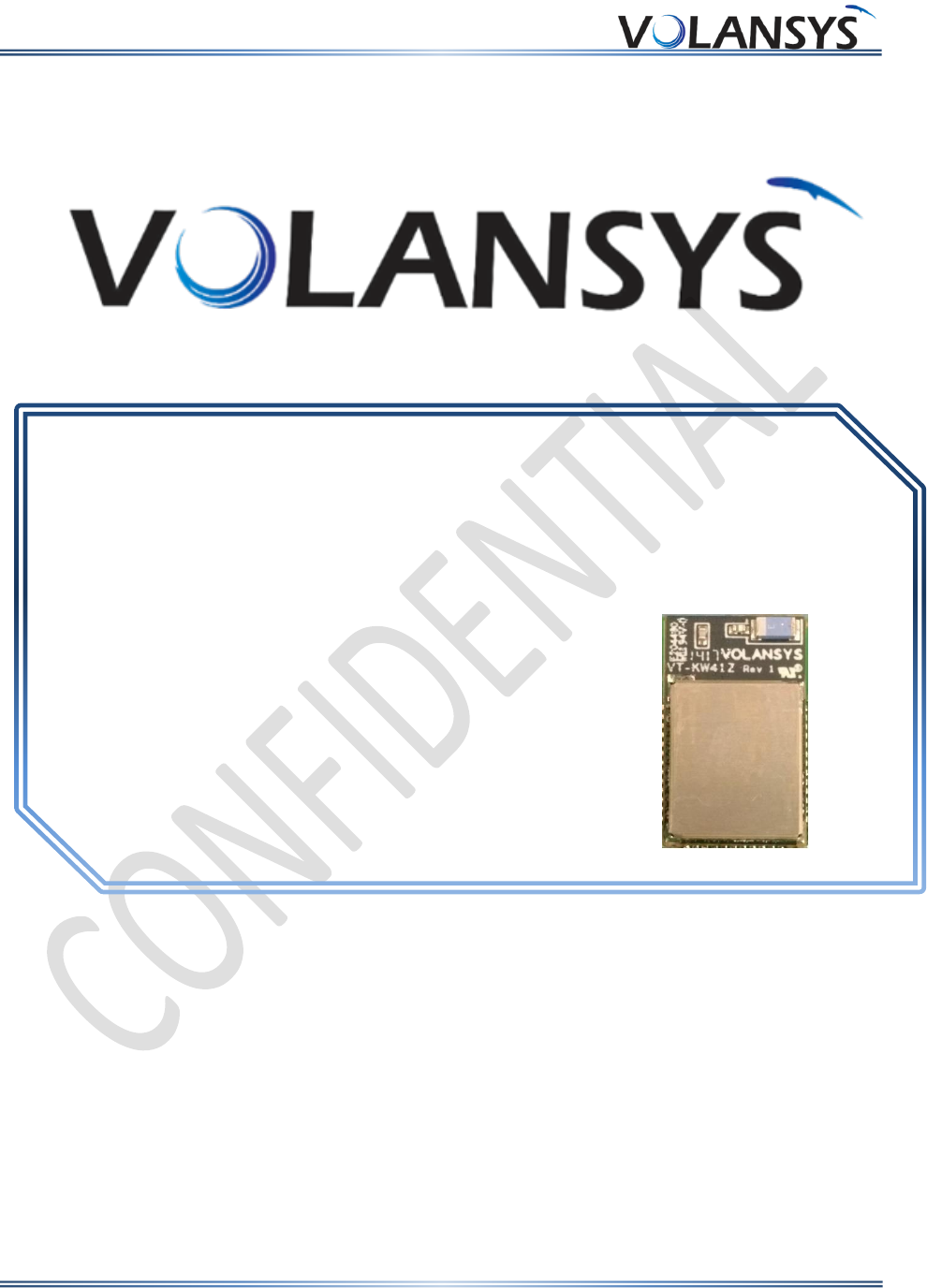
VT-MKW41Z MODULE
PRODUCT MANUAL
REVISION 0.4

VT-MKW41Z Module Datasheet
Rev 0.4 Confidential Copyright © 2017 Volansys
Volansys Technologies Page | 2
Copyright Info
The information contained in this document is the proprietary information of Volansys Technologies Pvt.,
Ltd. The contents are confidential and any disclosure to persons other than the officers, employees,
agents or subcontractors of the owner or licensee of this document, without the prior written consent of
Volansys, is strictly prohibited.
Further, no portion of this document may be reproduced, stored in a retrieval system, or transmitted in
any form or by any means, electronic or mechanical, including photocopying and recording, without the
prior written consent of Volansys, the copyright holder.
Volansys publishes this document without making any warranty as to the content contained herein.
Further Volansys reserves the right to make modifications, additions and deletions to this document due
to typographical errors, inaccurate information, or improvements to products mentioned in the document
at any time and without notice. Such changes will, nevertheless be incorporated into new editions of this
document.

VT-MKW41Z Module Datasheet
Rev 0.4 Confidential Copyright © 2017 Volansys
Volansys Technologies Page | 3
TABLE OF CONTENTS
1 DOCUMENT DETAILS ...................................................................................................................6
1.1 REVISION HISTORY ............................................................................................................................. 6
1.2 REFERENCES ..................................................................................................................................... 6
2 INTRODUCTION ..........................................................................................................................7
3 PRODUCT OVERVIEW ..................................................................................................................8
4 MODULE PINOUTS ......................................................................................................................9
5 HARDWARE DESCRIPTION ......................................................................................................... 14
5.1 HARDWARE BLOCK DIAGRAM ............................................................................................................ 14
5.2 ANTENNA ....................................................................................................................................... 15
5.3 MODULE RESET ............................................................................................................................... 15
5.4 CLOCK ........................................................................................................................................... 15
5.5 DEBUG AND PROGRAMMING ............................................................................................................. 16
6 ELECTRICAL CHARACTERISTICS .................................................................................................. 17
6.1 ABSOLUTE MAXIMUM RATINGS ......................................................................................................... 17
6.2 RECOMMENDED (OPERATING CONDITION) .......................................................................................... 17
6.3 DC-DC CONVERTER ......................................................................................................................... 17
6.3.1 Buck mode ........................................................................................................................... 18
6.3.2 Bypass Mode ....................................................................................................................... 18
6.3.3 Boost Mode ......................................................................................................................... 18
6.4 DC ELECTRICAL CHARACTERISTICS ...................................................................................................... 18
6.5 DIGITAL I/O SPECIFICATION............................................................................................................... 19
6.6 ANALOG AND VREF ......................................................................................................................... 19
6.7 RF CHARACTERISTICS ....................................................................................................................... 20
7 MODULE DIMENSION ............................................................................................................... 21
7.1 MKW41Z MODULE DIMENSION ....................................................................................................... 21
7.2 RECOMMENDED PCB LAYOUT PATTERN .............................................................................................. 22
8 CERTIFICATIONS ....................................................................................................................... 23
9 REGULATORY STATEMENTS ...................................................................................................... 24
9.1 FCC STATEMENT .......................................................................................................................... 24
9.2 FCC RADIATION EXPOSURE STATEMENT .............................................................................................. 24
9.3 ORIGINAL EQUIPMENT MANUFACTURER (OEM) NOTES ............................................................ 24
9.4 IC STATEMENT ................................................................................................................................ 25
9.5 CE REGULATORY ............................................................................................................................. 26
10 RECOMMENDED REFLOW PROFILE ........................................................................................ 27

VT-MKW41Z Module Datasheet
Rev 0.4 Confidential Copyright © 2017 Volansys
Volansys Technologies Page | 4
11 APPLICATION NOTE ............................................................................................................... 28
11.1 SAFETY PRECAUTIONS ...................................................................................................................... 28
11.2 DESIGN ENGINEERING NOTES ............................................................................................................ 28
11.3 STORAGE CONDITIONS ..................................................................................................................... 28
11.4 SHIPMENT ...................................................................................................................................... 28
11.5 HANDLING ...................................................................................................................................... 29
12 APPENDIX-A.......................................................................................................................... 30
12.1 ACRONYMS & GLOSSARY .................................................................................................................. 30

VT-MKW41Z Module Datasheet
Rev 0.4 Confidential Copyright © 2017 Volansys
Volansys Technologies Page | 5
LIST OF FIGURES
Figure 1: Module Overview ................................................................................................................9
Figure 2: MKW41Z Module Hardware Block Diagram ........................................................................ 14
Figure 3: MKW41Z Module Physical Dimensions ............................................................................... 21
Figure 4: PCB Layout Pattern Dimensions .......................................................................................... 22
Figure 5: Reflow Soldering Profile ..................................................................................................... 27
VT-MKW41Z Module Datasheet
Rev 0.4 Confidential Copyright © 2017 Volansys
Volansys Technologies Page | 6
1 DOCUMENT DETAILS
1.1 Revision History
Rev.
Date
Description
Prepared By
Reviewed By
Approved By
0.1
24-Aug-16
Initial draft version
released
Volansys
Volansys
Volansys
0.2
01-Dec-16
Rx and Tx mode power
consumption details
updated
Volansys
Volansys
Volansys
0.3
05-APR-17
Initial draft - as per new
module design -
Changes in Module pin-
out, configuration, PCB
form factor and layout
footprint suggestions
Volansys
Volansys
Volansys
0.4
13-Jun-17
FCC, IC and CE
regulatory statement
added
Volansys
Volansys
Volansys
1.2 References
Documents
Revision
MKW41Z512DS Datasheet - NXP
0.2

VT-MKW41Z Module Datasheet
Rev 0.4 Confidential Copyright © 2017 Volansys
Volansys Technologies Page | 7
2 INTRODUCTION
This document describes the Volansys MKW41Z module. Which has been designed to be easily integrated
into another device and to provide fast and low cost proven wireless network.
The MKW41Z module is ultra-compact, low power high sensitivity module. It is based on NXP’s
MKW41Z512VHT4 SoC combined with Bluetooth Low energy and IEEE 802.15.4 network stacks like
Thread, Zigbee pro etc.
No RF experience or expertise is required to add this powerful wireless networking capability to your
products. This series of modules offer fast integration opportunities and the shortest possible time to
market for your product.
VT-MKW41Z Module Datasheet
Rev 0.4 Confidential Copyright © 2017 Volansys
Volansys Technologies Page | 8
3 PRODUCT OVERVIEW
The MKW41Z Module is a fully self-contained, small form factor Bluetooth Low Energy 4.2 and IEEE
802.15.4 compliant module with low complexity and low power features. Based on NXP’s Kinetis MCU
wireless hardware platform, MKW41Z offers superior low power radio performance.
The MKW41Z module employs low power architecture and it has been optimized for all kind of application
in home automation, smart grid, smart lighting, also networked building control, Medical equipment and
Home automation application, HVAC and security.
For evaluation and development, Volansys also offers a complete set of evaluation and development
tools.
Module Features
Small form factor, SMT module 19mm x
11.51mm
Integrated chip antenna
Max output power: +3.5 dbm
Typical Receiver Sensitivity (BLE) = -96 dBm
Typical Receiver Sensitivity (802.15.4) = -100
dBm
32bit ARM® Cortex-M0+ MCU with 64K SRAM
and 512K Flash
Up to 48 MHz ARM® Cortex-M0+ core
Integrated DC-DC converter enables a wide
operating range from 0.9 V to 4.2 V
Supports Buck and boost power mode with
easy hardware configuration
Extended Operation temp range: -40 °C to
+105 °C
Hardware supported encryption AES 128-bit,
TRNG Supported
9 MCU Low-power modes to provide power
optimization based on application
requirements.
Low Power Mode (VLLS0) Current: ≈180 nA
All MCU pins accessible
Serial wire debug(SWD) Interface and Micro
Trace buffer
On module 32MHz crystal
External RTC 32KHz support
RoHS compliant
Peripheral Interfaces: 2xSPI, 1xUART, 2xI2C,
CMT, SWD, 16-bit ADC, Timers
Suggested Applications
Extremely low-power embedded systems
Portable health care devices
Wearable sports
Fitness devices
Computer keyboards and mice
Gaming controllers
Access control
Security systems
Smart energy
Home area networks
Automated meter reading
Medical Network
HVAC Control
Lighting control
Asset tracking
Environment monitoring and control
VT-MKW41Z Module Datasheet
Rev 0.4 Confidential Copyright © 2017 Volansys
Volansys Technologies Page | 9
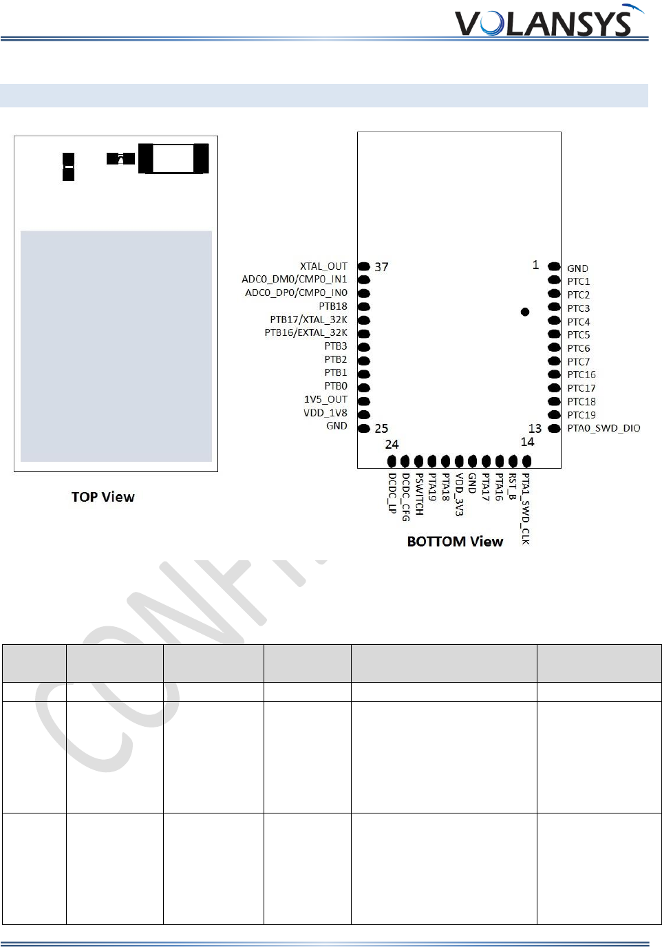
4 MODULE PINOUTS
Figure 1: Module Overview
MKW41Z module has 31 edge pin for connections as below:
Module
PIN#
MKW41Z512
PIN#
Name
Default
Use
Alternate Function
Remarks
1
26, 49 to 64
GND
2
37
PTC1
DISABLED
PTC1,
ANT_B,
I2C0_SDA,
UART0_RTS_b,
TPM0_CH2,
RF_ACTIVE
3
38
PTC2
DISABLED
TSI0_CH14/DIAG1,
PTC2/LLWU_P10,
TX_SWITCH,
I2C1_SCL,
UART0_RX,
CMT_IRO,
VT-MKW41Z Module Datasheet
Rev 0.4 Confidential Copyright © 2017 Volansys
Volansys Technologies Page | 10
DTM_RX
4
39
PTC3
DISABLED
TSI0_CH15/DIAG2,
PTC3/LLWU_P11,
RX_SWITCH,
I2C1_SDA,
UART0_TX,
TPM0_CH1,
DTM_TX
5
40
PTC4
DISABLED
TSI0_CH0/DIAG3,
PTC4/LLWU_P12,
ANT_A,
EXTRG_IN,
UART0_CTS_b,
TPM1_CH0,
BSM_DATA
6
41
PTC5
DISABLED
TSI0_CH1/DIAG4,
PTC5/LLWU_P13,
RF_OFF,
LPTMR0_ALT2,
UART0_RTS_b,
TPM1_CH1,
BSM_CLK
7
42
PTC6
DISABLED
TSI0_CH2,
PTC6/LLWU_P14/XTAL_OU
T_EN,
I2C1_SCL,
UART0_RX,
TPM2_CH0,
BSM_FRAME
8
43
PTC7
DISABLED
TSI0_CH3,
PTC7/LLWU_P15,
SPI0_PCS2,
I2C1_SDA,
UART0_TX,
TPM2_CH1,
BSM_DATA
9
45
PTC16
DISABLED
TSI0_CH4,
PTC16/LLWU_P0,
SPI0_SCK,
I2C0_SDA,
UART0_RTS_b,
TPM0_CH3
10
46
PTC17
DISABLED
TSI0_CH5,
PTC17/LLWU_P1,
SPI0_SOUT,
I2C1_SCL,
UART0_RX,

VT-MKW41Z Module Datasheet
Rev 0.4 Confidential Copyright © 2017 Volansys
Volansys Technologies Page | 11
BSM_FRAME,
DTM_RX
11
47
PTC18
DISABLED
TSI0_CH6,
PTC18/LLWU_P2,
SPI0_SIN,
I2C1_SDA,
UART0_TX,
BSM_DATA,
DTM_TX
12
48
PTC19
DISABLED
TSI0_CH7,
PTC19/LLWU_P3,
SPI0_PCS0,
I2C0_SCL,
UART0_CTS_b,
BSM_CLK,
RF_ACTIVE
13
1
PTA0
SWD_DIO
TSIO_CH8,
PTA0,
SPI0_PCS1,
TPM1_CH0,
SWD_DIO
Provide 10K pull
up
14
2
PTA1
SWD_CLK
TSI0_CH9,
PTA1,
SPI1_PCS0,
TPM1_CH1,
SWD_CLK
Provide 10K ohm
pull-down
15
3
PTA2/
RESET_b
RESET_b
PTA2,
TPM0_CH3,
RESET_b
Provide 10K pull
up
16
4
PTA16
DISABLED
TSI0_CH10
PTA16/LLWU_P4,
SPI1_SOUT,
TPM0_CH0
17
5
PTA17
DISABLED
TSI0_CH11,
PTA17/LLWU_P5/RF_RESET
,
SPI1_SIN,
TPM_CLKIN1
18
26, 49 to 64
GND
GND
19
10, 8
VIN
Supply
Input
20
6
PTA18
DISABLED
TSI0_CH12,
PTA18/LLWU_P6,
SPI1_SCK,
TPM2_CH0
21
7
PTA19
DISABLED
TSI0_CH13/ADC0_SE5,
PTA19/LLWU_P7,
VT-MKW41Z Module Datasheet
Rev 0.4 Confidential Copyright © 2017 Volansys
Volansys Technologies Page | 12
SPI1_PCS0,
TPM2_CH1
22
8
PSWITCH
VIN
23
9
DCDC_CFG
DCDC_CFG
24
11
DCDC_LP
DCDC_LP
25
26, 49 to 64
GND
GND
26
14
VDD_1P8OUT
27
15
VDD_1P5OUT
_PMCIN
28
16
PTB0
DISABLED
PTB0/LLWU_P8/XTAL_OUT
_EN,
PTB0,
I2C0_SCL,
CMP0_OUT,
TPM0_CH1,
CLKOUT
29
17
PTB1
DISABLED
ADC0_SE1/CMP0_IN5,
PTB1,
DTM_RX,
I2C0_SDA,
LPTMR0_ALT1,
TPM0_CH2,
CMT_IRO
30
18
PTB2
DISABLED
ADC0_SE3/CMP0_IN3,
PTB2,
RF_OFF,
DTM_TX,
TPM1_CH0
31
19
PTB3
DISABLED
ADC0_SE2/CMP0_IN4,
PTB3,
CLKOUT,
TPM1_CH1,
RTC_CLKOUT
32
21
EXTAL32K
EXTAL32K
EXTAL32K,
PTB16,
I2C1_SCL,
TPM2_CH0
33
22
XTAL32K
XTAL32K
XTAL32K,
PTB17,
I2C1_SDA,
TPM2_CH1,
BSM_CLK
34
23
PTB18
NMI_b
DAC0_OUT/ADC0_SE4/CM
P0_IN2,
PTB18,
I2C1_SCL,
TPM_CLKIN0,

VT-MKW41Z Module Datasheet
Rev 0.4 Confidential Copyright © 2017 Volansys
Volansys Technologies Page | 13
TPM0_CH0,
NMI_b
35
24
ADC0_DP0
ADC0_DP0
/
CMP0_IN0
ADC0_DP0 / CMP0_IN0
36
25
ADC0_DM0
ADC0_DM0
/
CMP0_IN1
ADC0_DM0/ CMP0_IN1
37
29
XTAL_OUT
XTAL_OUT
Note:
- Provided pull up at Reset_b pin.
- Provide Pull down at SWD_CLK pin.
- Provide Pull up at SWD_DIO pin.
VT-MKW41Z Module Datasheet
Rev 0.4 Confidential Copyright © 2017 Volansys
Volansys Technologies Page | 14
5 HARDWARE DESCRIPTION
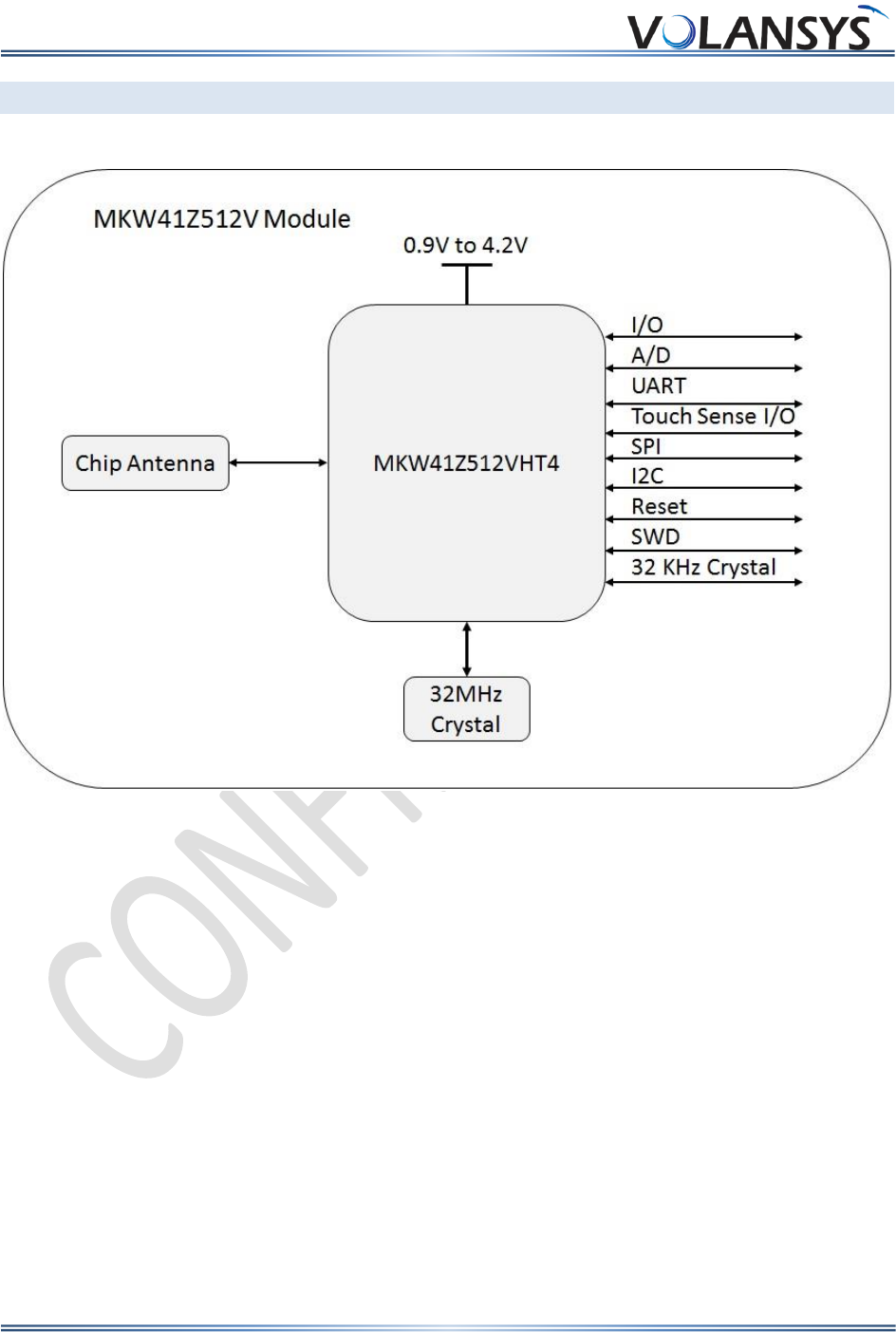
5.1 Hardware Block Diagram
Figure 2: MKW41Z Module Hardware Block Diagram
The MKW41Z512 Module families are based on the NXP’s Kinetis MCU family MKW41Z512VHT4. MKW41Z
module are fully integrated 2.4GHz Bluetooth Low Energy (BLE 4.2) and IEEE 802.15.4 compliant
transceiver and a powerful 32-bit ARM® Cortex M0+ MCU, up to 512kB flash and 128kB SRAM memory
and rich peripherals. The industry standard Micro trace buffer and serial wire SWD programming and
debugging interfaces together with the standard ARM system debug components help to streamline any
custom software development.
Module has inbuilt chip antenna. These antenna supports BLE and IEEE 802.15.4 protocol ISM Band
(2.4GHz). The voltages are monitored (brown-out detection) and the built in power-on-reset circuit
eliminates the need for any external monitoring circuitry. This module has support of external RTC
32/32.768 kHz watch crystal. The MKW41Z512 module have fully integrated DC-DC converter with Buck,
Boost and Bypass modes. Module can be easily configured for Buck and Boost mode power operations.
For more details please check DCDC converter section.

VT-MKW41Z Module Datasheet
Rev 0.4 Confidential Copyright © 2017 Volansys
Volansys Technologies Page | 15
5.2 Antenna
The MKW41z Module includes an integrated chip antenna. The MKW41Z Module should be mounted with
the PCB chip antenna overhanging the edge of the host board. To further improve performance, a ground
plane may be placed on the host board under the module up to the antenna keep out area. The installation
of an uninterrupted ground plane on a layer directly beneath the module will also allow you to run traces
under this layer.
The chip antenna is compact and highly efficient. To maximize range, an adequate ground plane must be
provided on the host PCB. Correctly positioned, the ground plane on the host PCB will contribute
significantly to the antenna performance; it should not be directly under the chip antenna. The position
of the module on the host board and overall design of the product enclosure contribute to antenna
performance. Poor design affects radiation patterns and can result in reflection, diffraction and/or
scattering of the transmitted signal.
A few design guidelines to help ensure antenna performance:
• Never place the ground plane or route copper traces directly underneath the antenna portion of the
module
• Never place the antenna close to metallic objects
• In the overall design, ensure that wiring and other components are not placed near the antenna
• Do not place the antenna in a metallic or metalized plastic enclosure
• Keep plastic enclosures 1cm or more away from the antenna in any direction
5.3 Module Reset
Pin 15 is used as an external reset. The reset pin only contains an active pull down device. This pin can be
used for other functions, such as GPIO, by setting the RESET_PIN_CFG option bit of the FTFA_FPORT
register to 0. This bit is retained through system resets and low power modes. When the RESET pin is
disabled and configured as a GPIO output, it operates as a pseudo open drain output.
5.4 Clock
The MKW41z Module requires two clock system.
On module 32MHz crystal used for RF reference oscillator. The clock is used by the RF, analog and digital
section interfaces. It can be used also by the MCU core and as a clock source for some internal peripherals.
For normal run modes, an internal oscillator can provide the low frequency clock. However, to make full
use of reduced power modes an external crystal must be present.
The MKW41z Module supports external 32/32.768KHz crystal. This is used as the clock for the RTC and
the deep-sleep clock.
Symbol
Parameter
Typ.
Max.
Unit
FNOM_LFXO
Crystal frequency
32/32.768
-
KHz
FTOL_LFXO_BLE
Frequency tolerance, BLE applications
±20
±250
ppm
CL_LFXO
Load Capacitance
7
12.5
pF
Note: External capacitors are not required for 32KHz crystal.

VT-MKW41Z Module Datasheet
Rev 0.4 Confidential Copyright © 2017 Volansys
Volansys Technologies Page | 16
5.5 Debug and Programming
The MKW41z module supports the two pin Serial Wire Debug (SWD) interface and offers flexible
mechanisms for non-intrusive debugging of program code. The R41Z also supports Micro Trace Buffer
(MTB) which provides a lightweight program trace capabilities using system RAM.
VT-MKW41Z Module Datasheet
Rev 0.4 Confidential Copyright © 2017 Volansys
Volansys Technologies Page | 17
6 ELECTRICAL CHARACTERISTICS
6.1 Absolute Maximum Ratings
The absolute maximum ratings given below should under no circumstances be violated. Exceeding one
or more of the limiting values may cause permanent damage to the device.
Description
Module
Unit
Min
Max
Power Supply Voltage (VIN)
-0.3
4.2
V
Voltage on I/O line
-0.3
VDD+0.3
V
RF Input power
-
+3.5
dbm
Storage temperature
-40
105
°C
6.2 Recommended (Operating Condition)
Description
Module
Unit
Min
Typ
Max
Bypass Mode Supply
Voltage(Digital) (VIN)
1.71
-
3.6
V
Boost Mode Supply Voltage (VIN)
0.9
-
1.795
V
Buck Mode Supply Voltage (VIN)1
2.1
-
4.2
V
RF Input Frequency
2360
2480
MHz
RF Output Power
-
-
3.5
dBm
SPI Clock Rate
-
-
12.0
MHz
Logic Input High voltage
0.7*VDD_1V83
-
-
V
Logic Input Low voltage
-
-
0.3*VDD_1V8
V
DC-DC Converter Output Power
-
-
125
mW
Ambient temperature
-40
25
105
°C
Note:
1. In Buck mode, DC-DC converter needs 2.1V min to start, the supply can drop to 1.8V after DC-DC
converter settles
2. Analog supply voltage is same as VDD_IO (VDD_1P8OUT)
3. VDD_1V8 is internal configurable LDO output referred as VDD_1P8OUT.
6.3 DC-DC Converter
The MKW41z module contains an integrated DCDC converter which allows for three modes of operation
without additional components. When operating in DCDC Buck mode, power consumption from using
the radio can be reduced compared to DCDC Bypass mode. DCDC Boost mode allows the use of a single
alkaline or other low voltage source. While it is possible to switch between these modes in a single
design.
VT-MKW41Z Module Datasheet
Rev 0.4 Confidential Copyright © 2017 Volansys
Volansys Technologies Page | 18
6.3.1 Buck mode
Pin No#
Net name
Connection
19
Power Supply Voltage (VIN)
1.8V - 4.2V VIN
23
DCDC_CFG
1.8V - 4.2V VIN
24
DCDC_LP
NC
22
PSWITCH1
1.8V - 4.2V VIN
26
V1P8
NC / 1.8V - 3.0 Output voltage2
27
V1P5
NC
Note 1: DCDC converter enables once PSWITCH connected with VIN supply. Once DCDC converter
started PSWITCH can be reconnected to GND without disrupting the DCDC converter operation.
Note 2: While DCDC converter is running in either Buck or boost mode, V1P8 is I/O level for MKW41z.
In Buck mode, V1P8 cannot output voltage greater than VIN supply voltage. V1P8 can provide a
limited number of additional peripheral devices which connect directly to the MKW41z’s IO due to
low output current. Please refer MKW41z datasheet for output current.
6.3.2 Bypass Mode
Pin No#
Net name
Connection
19
Power Supply Voltage (VIN)
1.71V - 3.6V VIN
23
DCDC_CFG
1.71V - 3.6V VIN
24
DCDC_LP
NC
22
PSWITCH
Ground
26
V1P8
1.71V - 3.6V VIN
27
V1P5
1.45V - 3.6V VIN
6.3.3 Boost Mode
Pin No#
Net name
Connection
19
Power Supply Voltage (VIN)
0.9V - 1.8V VIN
23
DCDC_CFG
Ground
24
DCDC_LP
0.9V - 1.8V VIN
22
PSWITCH
0.9V - 1.8V VIN
26
V1P8 Out
NC / 1.8V - 3.0V Output voltage1
27
V1P5
NC
Note 1: While DCDC converter is running in either Buck or boost mode, V1P8 is I/O level for MKW41z.
V1P8 can provide a limited number of additional peripheral devices which connect directly to the
MKW41z’s IO due to low output current. Please refer MKW41z datasheet for output current.
6.4 DC Electrical Characteristics
Buck Mode, VIN=3.6V, Tamb = 25°C, unless otherwise Specified
Description
Module
Unit
Min
Typ
Max
Transmit mode current @
+TBDdBm
-
TBD
-
mA
Receive mode current @max
sensitivity
-
TBD
-
mA
VT-MKW41Z Module Datasheet
Rev 0.4 Confidential Copyright © 2017 Volansys
Volansys Technologies Page | 19
Idle mode- Normal run, CPU at
48MHz
4
mA
Please Note:
- The average current consumption during operation is dependent on the firmware and the network load.
6.5 Digital I/O Specification
Digital I/Os of MKW41Z512 Module, VIN = 3.3V, Tamb = 25°C, unless otherwise Specified
Symbol
Description
Module
Unit
Min
Typ
Max
VOH
Output high voltage — high drive
strength
• 2.7 V ≤ VDD ≤ 3.6 V, IOH = -20 mA
• 1.71 V ≤ VDD ≤ 2.7 V, IOH = -10 mA
VDD-0.5
-
-
V
Output high voltage — low drive
strength
• 2.7 V ≤ VDD ≤ 3.6 V, IOH = -5 mA
• 1.71 V ≤ VDD ≤ 2.7 V, IOH = -2.5 mA
VDD-0.5
-
-
V
IOHT
IOHT Output high current total for all
ports
-
-
100
mA
VOL
Output low voltage — high drive
strength
• 2.7 V ≤ VDD ≤ 3.6 V, IOL = 20 mA
• 1.71 V ≤ VDD ≤ 2.7 V, IOL = 10 mA
-
-
0.5
V
Output low voltage — low drive
strength
• 2.7 V ≤ VDD ≤ 3.6 V, IOL = 5 mA
• 1.71 V ≤ VDD ≤ 2.7 V, IOL = 2.5 mA
-
-
0.5
V
VOLT
IOLT Output low current total for all
ports
-
-
100
mA
RESET_b
Reset Pulse width to guarantee a reset
100
-
-
ns
6.6 Analog and VREF
The ADC analog system VDDA powered with 1.8V supply through filtering circuit onboard the MKW41z
module. The voltage reference VREF, has two sourcing options: internal and external supply. When
externally supplied, VREF should be referenced to VDDA. And for internal reference voltage, buffered
reference is available internally for use with on chip peripherals such as ADCs and DACs. The Voltage
Reference output can be trimmed with a resolution of 0.5mV
Symbol
Description
Module
Unit
Min
Typ
Max
VDDA
Analog supply voltage
1.71
1.8
1.8
V
VREFH
ADC reference voltage high
1.13
VDDA
VDDA
V
VREF_OUT
Voltage reference output
1.19
1.195
1.2
V
VADIN
16-bit differential mode
GND
31/32 × VREFH
V
VT-MKW41Z Module Datasheet
Rev 0.4 Confidential Copyright © 2017 Volansys
Volansys Technologies Page | 20
All other modes
GND
VREFH
V
VAIN
Analog input voltage
GND - 0.3
VDD
V
VAIO
Analog input offset voltage
-
-
20
mV
IDDHS
Supply current, High-speed mode
-
-
200
uA
IDDLS
Supply current, low-speed mode
-
-
20
uA
VCMPOh
Comparator output high
VDD - 0.5
-
-
V
VCMPOl
Comparator output low
-
-
0.5
V
6.7 RF Characteristics
Description
Module
Unit
Min
Typ
Max
RF Frequency range
2400
-
2483.5
MHz
Tx Power
-30
-
+3.5
dBm
BLE Rx Sensitivity
-
-96
-
dBm
IEEE 802.15.4 Rx Sensitivity
-
-100
-
dBm
GFSK Rx Sensitivity (250 kbps GFSK-
BT=0.5, h=0.5)
-
-100
-
dBm
VT-MKW41Z Module Datasheet
Rev 0.4 Confidential Copyright © 2017 Volansys
Volansys Technologies Page | 21
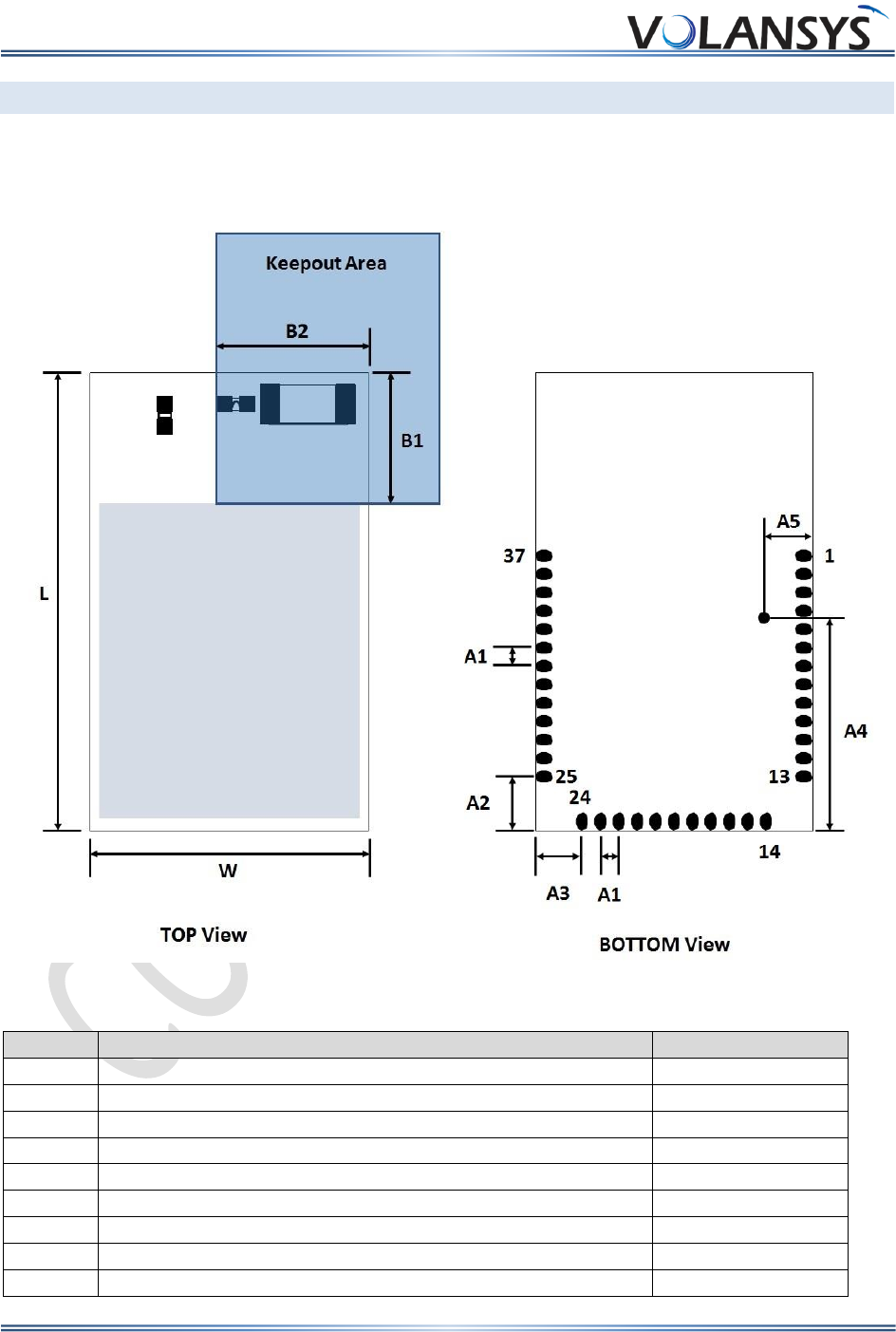
7 MODULE DIMENSION
7.1 MKW41z Module Dimension
Figure 3: MKW41Z Module Physical Dimensions
Symbol
Description
Typical Distance
L
Length of Module
19mm
W
Width of Modules
11.51mm
A1
SMD pad pitch
1.27mm
A2
Distance between board edge to center of pad
2.26
A3
Distance between board edge to center of pad
1.94
A4
Circular pad keepout from board edge
8.84mm
A5
Circular pad keepout from board edge
2mm
A
Keepout circular pad size
0.3mm
B1
Keepout zone from corner of PCB
6.5mm
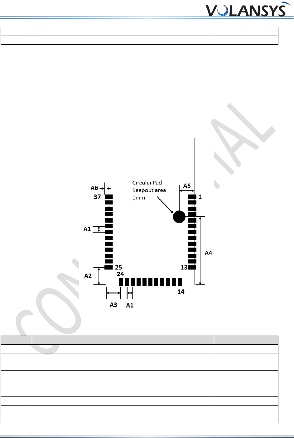
VT-MKW41Z Module Datasheet
Rev 0.4 Confidential Copyright © 2017 Volansys
Volansys Technologies Page | 22
B2
Keepout zone from corner of PCB
6.5mm
B x37
Rectangular SMD Pad size (All Pads are placed on board edges)
0.76mm x 0.50mm
For ideal RF performance when using the on-board antenna, the antenna should be located at the corner
of the carrier PCB. There should be no components, tracks or copper planes in the Keep-out area which
should be as large as possible.
When placing the module please either locate the antenna in the corner edge of PCB. So that the
recommended antenna keep out zone is being followed, or add a no copper zone as mentioned keep out
area.
7.2 Recommended PCB layout pattern
Figure 4: PCB Layout Pattern Dimensions
Symbol
Description
Typical Distance
A1
SMD pad pitch
1.27mm
A2
Distance between board edge to center of pad
2.26
A3
Distance between board edge to center of pad
1.94
A4
Circular pad keep-out from board edge
8.84mm
A5
Circular pad keep-out from board edge
2mm
A
circular pad Keepout area
1mm
B1
Keepout zone from corner of PCB
6.5mm
B2
Keepout zone from corner of PCB
6.5mm
B x37
Rectangular SMD Pad size (All Pads are placed on board edges)
1mm x 0.50mm

VT-MKW41Z Module Datasheet
Rev 0.4 Confidential Copyright © 2017 Volansys
Volansys Technologies Page | 23
8 CERTIFICATIONS
FCC: FCC part 15 modular certification ID: 2AKNO-MKW41Z
IC: Industry Canada RSS-247 modular certification IC:22256-MKW41Z
CE: EN 60950-1: 2006 + A11 :2009 + A1:2010 + A12:2011 + A2:2013
EN 301 489-1 V2.2.0 (2017-03)
EN 301 489-17 V3.2.0 (2017-03)
EN 300 328 V2.1.1

VT-MKW41Z Module Datasheet
Rev 0.4 Confidential Copyright © 2017 Volansys
Volansys Technologies Page | 24
9 REGULATORY STATEMENTS
9.1 FCC STATEMENT
1. This device complies with Part 15 of the FCC Rules. Operation is subject to the following two
conditions:
(1) This device may not cause harmful interference.
(2) This device must accept any interference received, including interference that may cause
undesired operation.
2. Changes or modifications not expressly approved by the party responsible for compliance
could void the user's authority to operate the equipment.
NOTE: This equipment has been tested and found to comply with the limits for a Class B digital
device, pursuant to Part 15 of the FCC Rules. These limits are designed to provide reasonable
protection against harmful interference in a residential installation.
This equipment generates uses and can radiate radio frequency energy and, if not installed and
used in accordance with the instructions, may cause harmful interference to radio
communications.
However, there is no guarantee that interference will not occur in a installation. If this
equipment does cause harmful interference to radio or television reception, which can be
determined by turning the equipment off and on, the user is encouraged to try to correct the
interference by one or more of the following measures:
Reorient or relocate the receiving antenna.
Increase the separation between the equipment and receiver.
Connect the equipment into an outlet on a circuit different from that to which the receiver is
connected.
Consult the dealer or an experienced radio/TV technician for help.
9.2 FCC Radiation Exposure Statement
This equipment complies with FCC radiation exposure limits set forth for an uncontrolled
environment. This equipment should be installed and operated with minimum distance 20cm
between the radiator & your body
9.3 ORIGINAL EQUIPMENT MANUFACTURER (OEM) NOTES
The OEM must certify the final end product to comply with unintentional radiators (FCC
Sections 15.107 and 15.109) before declaring compliance of the final product to Part 15
of the FCC rules and regulations. Integration into devices that are directly or indirectly c
onnected to AC lines must add with Class II Permissive Change.

VT-MKW41Z Module Datasheet
Rev 0.4 Confidential Copyright © 2017 Volansys
Volansys Technologies Page | 25
The OEM must comply with the FCC labeling requirements. If the module’s label is not
visible when installed, then an additional permanent label must be applied on the outside
of the finished product which states: “Contains transmitter module FCC ID: 2AKNO-
MKW41Z Additionally, the following statement should be included on the label and in
the final product’s user manual: “This device complies with Part 15 of the FCC Rules.
Operation is subject to the following two conditions: (1) This device may not cause
harmful interferences, and (2) this device must accept any interference received,
including interference that may cause undesired operation.”
The module is limited to installation in mobile or fixed applications. Separate approval is
required for all other operating configurations, including portable configuration with re
spect to Part 2.1093 and different antenna configurations.
module or modules can only be used without additional authorizations if they have been
tested and granted under the same intended end‐se operational conditions, including
simultaneous transmission operations. When they have not been tested and granted in
this manner, additional testing and/or FCC application filing may be required. The most
straightforward approach to address additional testing conditions is to have the grantee
responsible for the certification of at least one of the modules submit a permissive change
application.When having a module grantee file a permissive change is not practical or
feasible, the following guidance provides some additional options for host manufacturers.
Integrations using modules where additional testing and/or FCC application filing(s) may
be required are: (A) a module used in devices requiring additional RF exposure compliance
information (e.g., MPE evaluation or SAR testing); (B) limited and/or split modules not
meeting all of the module requirements; and (C) simultaneous transmissions for
independent collocated transmitters not previously granted together.
This Module is full modular approval; it is limited to OEM installation ONLY.
Integration into devices that are directly or indirectly connected to AC lines must add with Class II
Permissive Change.
(OEM) Integrator must assure compliance of the entire end product include the integrated
Module.
Additional measurements (15B) and/or equipment authorizations (e.g Verification) may need to
be addressed depending on co-location or simultaneous transmission issues if applicable.
(OEM) Integrator is reminded to assure that these installation instructions will not be made
available to the end user of the final host device.
9.4 IC Statement
This device complies with Industry Canada license‐exempt RSS standard(s). Operation is subject to
the following two conditions: (1) This device may not cause interference, and (2) This device must
accept any interference, including interference that may cause undesired operation of the device.
This device complies with RSS‐247 of Industry Canada. Operation is subject to the condition that

VT-MKW41Z Module Datasheet
Rev 0.4 Confidential Copyright © 2017 Volansys
Volansys Technologies Page | 26
this device does not cause harmful interference. This Class B digital apparatus complies with
Canadian ICES‐003 (Cet appareil numérique de la Classe B conforme à la norme NMB‐003 du
Canada).
This equipment(IC:22256-MKW41Z) complies with IC radiation exposure limits set forth for an
uncontrolled environment. This equipment should be installed and operated with minimum
distance of 20 cm between the radiator and your body. This transmitter must not be co-located or
operating in conjunction with any other antenna or transmitter.
Le présent appareil est conforme aux CNR d'Industrie Canada applicables aux appareils radio
exempts de licence. L'exploitation est autorisée aux deux conditions suivantes : (1) l'appareil ne
doit pas produire de brouillage, et (2) l'utilisateur de l'appareil doit accepter tout brouillage
radioélectrique subi, même si le brouillage est susceptible d'en compromettre le fonctionnement.
Cet équipement (IC: 22256-MKW41Z) est conforme aux limites IC d'exposition aux radiations
définies pour un environnement non contrôlé. Cet équipement doit être installé et utilisé avec une
distance minimale de 20 cm entre le radiateur et votre corps. Cet émetteur ne doit pas être situé
ou opérant en conjonction avec une autre antenne ou émetteur.
9.5 CE Regulatory
Max RF power:
BLE(2402-2480MHz): 3.8dBm
Thread(2400-2483.5MHz): 3.1dBm
RF exposure information: The Maximum Permissible Exposure (MPE) level has been calculated
based on a distance of d=20 cm between the device and the human body. To maintain compliance
with RF exposure requirement, use product that maintain a 20cm distance between the device and
human body.
Regulatory Conformance:
Hereby, VOLANSYS TECHNOLOGIES PVT. LTD. that the radio equipment type [VT-KW41Z]
is in compliance with Directive 2014/53/EU.
EU declaration of conformity is available at the following internet address: www.volansys.com
Notice: Observe the national local regulations in the location where the device is to be used. This
device may be restricted for use in some or all member states of the European Union (EU)
VT-MKW41Z Module Datasheet
Rev 0.4 Confidential Copyright © 2017 Volansys
Volansys Technologies Page | 27
10 RECOMMENDED REFLOW PROFILE
Recommended Reflow Profile
Parameters Values
Ramp Up Rate (from T soak max to T peak)
3°/sec max
Minimum Soak Temperature
150°C
Maximum Soak Temperature
200°C
Soak Time
90 30 sec
T Liquids
220°C
Time above TL
60-150 sec
T peak
250°C
Time within 5º of T peak
20-30 sec
Time from 25° to T peak
8 min max
Ramp Down Rate
6°C/sec max
Figure 5: Reflow Soldering Profile
Use of “No-Clean” solder paste is recommended to avoid the requirement for a cleaning process. Cleaning
the module is strongly discouraged because it will be difficult to ensure no cleaning agent and other
residuals are remaining underneath the shielding can as well as in the gap between the module and the
host board.
Please Note:
Maximum number of reflow cycles: 2
Opposite-side reflow is prohibited: Do not place the module on the bottom / underside of your PCB and
re-flow

VT-MKW41Z Module Datasheet
Rev 0.4 Confidential Copyright © 2017 Volansys
Volansys Technologies Page | 28
11 APPLICATION NOTE
11.1 Safety Precautions
These specifications are intended to preserve the quality assurance of products as individual components.
Before use, check and evaluate the module’s operation when mounted on your products. Abide by these
specifications when using the products. These products may short-circuit. If electrical shocks, smoke, fire,
and/or accidents involving human life are anticipated when a short circuit occurs, then provide the
following failsafe functions as a minimum:
(1) Ensure the safety of the whole system by installing a protection circuit and a protection device.
(2) Ensure the safety of the whole system by installing a redundant circuit or another system to prevent a
single fault causing an unsafe status.
11.2 Design Engineering Notes
(1) Heat is the major cause of shortening the life of the modules. Avoid assembly and use of the target
equipment in conditions where the product’s temperature may exceed the maximum allowable.
(2) Failure to do so may result in degrading of the product’s functions and damage to the product.
(3) If pulses or other transient loads (a large load applied in a short time) are applied to the products,
before use, check and evaluate their operation when assembled onto your products.
(4) These products are not intended for other uses, other than under the special conditions shown below.
Before using these products under such special conditions, check their performance and reliability under
the said special conditions carefully, to determine whether or not they can be used in such a manner.
(5) In liquid, such as water, salt water, oil, alkali, or organic solvent, or in places where liquid may splash.
In direct sunlight, outdoors, or in a dusty environment. In an environment where condensation occurs. In
an environment with a high concentration of harmful gas (ex. salty air, HCl, Cl2, SO2, H2S, NH3, and NOx)
(6) If an abnormal voltage is applied due to a problem occurring in other components or circuits, replace
these products with new products because they may not be able to provide normal performance even if
their electronic characteristics and appearances appear satisfactory.
(7) Mechanical stress during assembly of the board and operation has to be avoided.
(8) Pressing on parts of the metal cover or fastening objects to the metal cover is not permitted.
11.3 Storage Conditions
(1) The module must not be stressed mechanically during storage.
(2) Do not store these products in the following conditions or the performance characteristics of the
product, such as RF performance, may well be adversely affected:
(3) Storage in salty air or in an environment with a high concentration of corrosive gas, such as Cl2, H2S,
NH3, SO2, or NOX
(4) Storage (before assembly of the end product) of the modules for more than one year after the date of
delivery at your company even if all the above conditions (1) to (3) have been met, should be avoided.
11.4 Shipment
The MKW41Z Modules are delivered in trays of TBD.

VT-MKW41Z Module Datasheet
Rev 0.4 Confidential Copyright © 2017 Volansys
Volansys Technologies Page | 29
11.5 Handling
<TBD> The MKW41Z Modules are designed and packaged to be processed in an automated assembly line.
VT-MKW41Z Module Datasheet
Rev 0.4 Confidential Copyright © 2017 Volansys
Volansys Technologies Page | 30
12 APPENDIX-A
12.1 Acronyms & Glossary
The following terms are used in this document
Sr No#
Terms
Definition
1.
MCU
Microcontroller Unit
2.
CPU
Central Processing Unit
3.
BLE
Bluetooth Low Energy
4.
PWM
Pulse width Modulation
5.
ADC
Analog to Digital Convertor
6.
TBD
To Be Define
7.
MCU
Micro Controller Unit
8.
SRAM
Static Random Access Memory
9.
RTC
Real Time Clock
10.
NC
No Connection