Vytek 0006068662 Paging Station User Manual Serial InterfaceB
Vytek Inc Paging Station Serial InterfaceB
Vytek >
manual

Power Amplifier Serial I/F Spec.
1 Version 1.62
Power Amplifier Serial Interface
Version 1.62
Requirements Specification
Sonik Technologies Corporation
Sonik Technologies Corporation
2310 Cousteau Court
Vista, CA 92083
Ph: 760-536-1000
Fax: 760-536-1025
Power Amplifier Serial I/F Spec.
2 Version 1.62
Table of Contents
1. Introduction..................................................................................................................3
1.1 Version Control........................................................................................................3
1.2 Scope........................................................................................................................3
1.3 Overview..................................................................................................................3
2. Power Amplifier...........................................................................................................4
2.1 Status & Control ......................................................................................................4
2.2 Non-volatile read/write memory..............................................................................5
3. Microprocessor Interface .............................................................................................6
3.1 SPI BUS ID..............................................................................................................6
3.2 Serial Communication Description..........................................................................7
3.3 SPI Bus Interface .....................................................................................................7
3.4 Power Amplifier Device ID.....................................................................................8
3.5 SPI Electrical Considerations ..................................................................................9
3.6 Serial Communication Format.................................................................................9
3.7 SPI Session Protocol..............................................................................................10
3.7.1 Power Amplifier DeviceID 0 transfer protocol .............................................11
3.7.2 Power Amplifier DeviceID 1 transfer protocol .............................................12
3.7.3 Power Amplifier DeviceID 2 transfer protocol .............................................12
3.7.4 Power Amplifier DeviceID 3 transfer protocol .............................................12
3.7.5 Power Amplifier DeviceID 4 transfer protocol .............................................12

Power Amplifier Serial I/F Spec.
3 Version 1.62
1. Introduction
1.1 Version Control
Date Author Revision Comment
12/20/00 Welte 1.00 Initial Revision
12/21/00 Welte 1.10 Added more clarity to section 2.4 and changed Figure 2-1 to
specify host as Master and size of transaction.
1/4/01 Welte 1.20 Redefined chip select, device ID mechanism. Made some
changes to timing diagrams.
1/9/01 Welte 1.30 Changes made in accordance to design review, namely remove
the –RackEnable signal, specify backplane values, make some
error corrections.
1/10/01 JS 1.40 Elaborated on hardware issues.
3/30/01 G. Nakao 1.41
6/6/01 G. Nakao 1.42 SPI Refinements
6/7/01 RMS 1.61 Further clarifications
9/12/01 J.Briggs 1.62 SPI Timing changes
1.2 Scope
This document is a technical description of the RF Power Amplifier Serial Peripheral Interface
(SPI) requirements.
1.3 Overview
The Power Amplifiers operate at approximately 133 watts average power, and will be combined
in parallel to achieve 400 watts average power, or 1200 watts peak power. Amplifier status and
configuration is done via the SPI interface. The amplifier section is comprised of 3 modules.
Two SPI interface connectors are to be located on the rear of each amplifier module. The SPI
interface is routed to each individual amplifier within the amplifier by daisy chain wiring.
In the event of an amplifier failure, the remaining amplifiers continue to operate, providing
continuous performance and soft fail operation. Failed amplifiers indicate their status via the SPI
interface.
The Power Amplifier must be capable of collecting and sending over the serial bus amplifier
status including:
temperature
forward power
reflected power
attenuator level
phase setting
Power Amplifier Serial I/F Spec.
4 Version 1.62
DC supply voltage
DC supply current
fan status
internal self- test result
amplifier model number
2. Power Amplifier
2.1 Status & Control
The Power Amplifier has status & control information as defined in Table 2.1:

Power Amplifier Serial I/F Spec.
5 Version 1.62
Description No. of
Bits Definition Read/Write
Temperature 8 0 = 0C
255 = -1C
206 = -50C
100 = +100C
Read only
Forward Power 8 0 = 0 Watts
1 = 1 Watts
255 = 255 Watts
Read only
Reflected Power 8 0 = 0 Watts
1 = 1 Watts
255 = 255 Watts
Read only
DC Supply Voltage 8 0 = 0 Volts
255 = 30V Read only
DC Supply Current 8 0 = 0 Amps
255 = 40 amps Read only
Fan Fail Alarm 1 0 = Normal, 1 = Alarm Occurred Read only
Amplifier Online 1 0= offline, 1=enabled Read/Write
Amplifier Reset 1 0 = Normal, 1 = Reset Occurred Read/Write
Reverse Power
Shutdown 1 0 = Normal, 1 = Shutdown Occurred
Read/Write
Amplifier Overdrive
Alarm 1 0 = Normal, 1 = Alarm Occurred Read/Write
Thermal Alarm 1 0 = Normal, 1 = Alarm Occurred Read/Write
Amplifier Overdrive
Shutdown 1 0 = Normal, 1 = Shutdown Occurred Read/Write
Thermal Alarm
Shutdown 1 0 = Normal, 1 = Shutdown Occurred Read/Write
Phase Control 8 -128 = -20 degrees min (in 40 steps)
0 = 0 degrees
+127 = +20 degrees min (in 40 steps)
Write Only
Attenuation Level 8 0 = -2 dB min (in 40 steps)
63 = No attenuation
127 = +2 dB min (in 40 steps)
Write Only
Serial Number 256 Read only
Table 2-1
2.2 Non-volatile read/write
In addition, the Power Amplifier contains 256 bytes of non-volatile read/write memory for
storing phase control and attenuation levels for various channel frequencies. The manufacturer
will be responsible for initializing correct attenuation & phase values for all frequencies, as well
as model and version numbers.
The memory content and locations are defined in Table 2-2:

Power Amplifier Serial I/F Spec.
6 Version 1.62
0Table 2-2
3. Microprocessor Interface
The microprocessor interface provides serial communication between the Power Amplifier and
external microprocessor/microcontroller (host). Through this interface, the Power Amplifier will
send information to the host and the host will send information to the Power Amplifier. The SPI
interface is a standard CPU interface, common on PIC and Motorola CPUs. As a point of
reference, the 68HC11 CPU is the classic implementation of the SPI, and is the reference used at
Sonik for the operation of the SPI bus.
Along with the SPI signals, there are 6 address lines on the SPI interface connector. These
address lines are used to determine which device on the SPI bus is being addressed, as well as
which information within the device is being addressed. The 6 address lines are split into 3
device select lines (device ID 0-7), and 3 register select lines.
3.1 SPI BUS ID
Each module on the SPI BUS will have an ID value as described in Table 3.1. When the address
lines associated with the device ID match the module’s ID, the module is to respond.
Relative
Offset Page Address Description
0 0 940 MHz Attenuation Value
1 940 MHz Phase Value
2 Unused
3 Unused
4 1 930 MHz Attenuation Value
5 930 MHz Phase Value
. Unused
. Unused
. 2 Unused
. Unused
216 0x36 Serial Number (32 bytes starting at 0xD8)
. “
. “
. “
247 Serial Number
248 0x3E Model Number
249 Version Number
250 Unused
251 Unused
252 0x3F Unused
253 Unused
254 Unused
255 Checksum

Power Amplifier Serial I/F Spec.
7 Version 1.62
0Table 3-1
3.2 Serial Communication Description
The Power Amplifier and host will communicate synchronously via a Serial Peripheral Interface
(SPI) Bus with the master located on the host and the Power Amplifier functioning as one of up
to 8 slave devices.
3.3 SPI Bus Interface
The SPI interface on the PA shall use a DB15 male connector as the primary interface
(designated SPI1), and a DB15 female connector (designated SPI2) as a daisy-chain interface.
All pins on both connectors will be wired in parallel. All pins will be RF bypassed, and all input
pins will have 10kO resistive pull-ups to +5V internal to the amplifier. The capacitive loading
on each pin shall not exceed 100pF.
The connector cable between the SPI control unit and first PA, and the daisy chain cables used to
connect between the 4 PAs will have wires only for pins 1-10. Pins 11 and 12 will be tied to pin
15 or left open inside each SPI1 input connector shell, in order to select the PA number. Pin 14
may be used for DC power to other SPI devices. No more than 25mA should be drawn from pin
14 by any SPI device. The DC power on pin 14 comes from the SCM board in the controller.
The SPI bus interface connector pin outs are described in Table 3-2:
Pin Description Pin Description
1 Shield GND 9 SPI MOSI
2 SPI A5 10 SPI MISO
3 SPI A4 11 Backplane ID0
4 SPI A3 12 Backplane ID1
5 SPI A2 13 Reset
6 SPI A1 14 +10-15VDC from
controller.
7 SPI A0 15 GND
8 SPI CLK
System Devices ID
(A5, A4, A3)
Reserved 0 0 0
Power Amplifier #1 0 0 1
Power Amplifier #2 0 1 0
Power Amplifier #3 0 1 1
Power Amplifier #4 1 0 0
Power Supply #1 1 0 1
Power Supply #2 1 1 0
Reserved 1 1 1

Power Amplifier Serial I/F Spec.
8 Version 1.62
0Table 3-2
Note: Pins 11 and 12 will indicate to the amplifier its slot location in the rack.
Pin 11 Pin 12 Amplifier
Ground Ground 1
Ground Open 2
Open Ground 3
Open Open 4
Pins 13, 14, and 15 should be left open in the Sonik rack.
These pins will be used by the manufacturer for test purposes.
SPI bits A5-A3 are used to select the Power Amplifier module on the SPI BUS. SPI bits A2-A0
are used to select the register/device within the selected Power Amplifier module.
3.4 Power Amplifier Device ID
The Power Amplifier shall have SPI “devices” associated with SPI A2-A0 defined in Table 3-3:
Device
ID Definition Device Size
(in bytes)
0 Temperature (read only)
Forward Power (read only)
Reflected Power (read only)
DC supply voltage (read only)
DC supply current (read only)
5
Status word (Read Only) For all bits except bit 6, the amplifier sets the bit
when the relevant condition occurs. The bit will stay set until cleared by a
write of a 1 to the corresponding bit in the control register. Bit 6 indicates
whether the amplifier is active or shut down. The amplifier may only be
brought online by writing a 1 to bit 6 of the control register, but shutdown
may occur either by writing a 0 to bit 6 of the control register, or by one of
the shutdown conditions being detected.
7 6 5 4 3 2 1 0
1
Fan
Fail
Flag
Amp
Online Amplifier
Reset Flag Reverse
Power
Shutdown
Flag
Amplifier
Overdrive
Alarm
Flag
Thermal
Alarm
Flag
Amplifier
Overdrive
Shutdown
Flag
Thermal
Shutdown
Flag
1
2 Phase Control (write only) 1
3 Attenuation Level (write only) 1
4 EEPROM (read/write) 4
Control word (write only) 5
7 6 5 4 3 2 1 0
1
Power Amplifier Serial I/F Spec.
9 Version 1.62
Fan
Fail
Flag
Clear
Amp
Online
Amplifier
Reset Flag
Clear
Reverse
Power
Shutdown
Flag Clear
Amplifier
Overdrive
Alarm
Flag Clear
Thermal
Alarm
Flag
Clear
Amplifier
Overdrive
Shutdown
Flag Clear
Thermal
Shutdown
Flag Clear
6 Reserved
7 Factory Communication
0Table 3-3
3.5 SPI Electrical Considerations
All signals are CMOS levels with 30%/70% thresholds. Devices driving the SPI bus must be
able to drive a load of 500 ohms // 2200pF with a rise-time of less than 1uS. The SN65176B
transceiver from TI is a recommended I/O device. It is differential, but can be used in a single-
ended mode.
3.6 Serial Communication Format
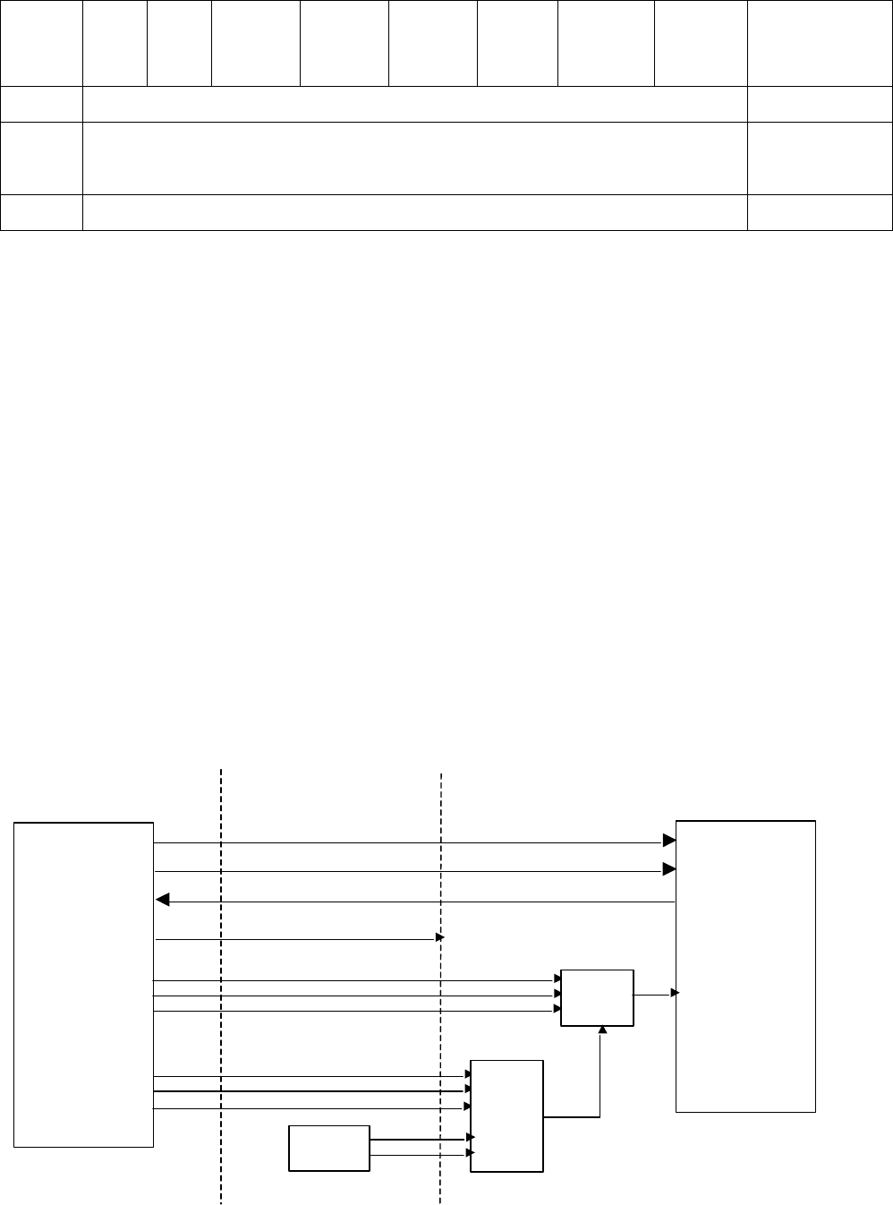
Figure 3-1 below shows the connection between the host and the Power Amplifier:
CLK
MOSI
MISO
B+ (10-
15VDC
out)
A2,A1,A0
A5,A4,A3
SPIC
SPII
SPIO
SPISB
Backplane
ID
PA
Compare
Host
Control
Interface
DB15 SPI 1
Connector Shell
PA SPI
Device
Interface
Device
Select
2,3,4
5,6,7
8
9
10
11,12
14

Power Amplifier Serial I/F Spec.
10 Version 1.62
Figure 3-1
Note that the Host is the Master Device and therefore is the only device on the SPI bus to drive
the CLK signal.
The host changes its MOSI output on the falling edge of the SPI clock while the SPISB (chip
selected) is driven active low. The Power Amplifier is expected to sample data (SPII) on the
rising edge of the clock signal.
The host samples the MISO input on the rising edge of the SPI clock while the SPISB (chip
selected) is driven active low. The Power Amplifier is expected to change its output (SPIO) on
the falling edge of the SPI clock.
SPI transfers are variable length depending on the SPI device (refer to Table 3-3). During an SPI
transfer, data is transmitted and received simultaneously.
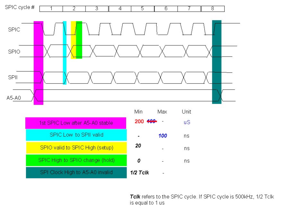
3.7 SPI Session Protocol
All SPI transfers are started and controlled by the host. A SPI transfer is started after the Power
Amplifier device address A5..A0 is selected and is complete when the address changes. The
address will always return to an inactive state (ie no SPI device within the system is selected).
SPI transfers in packets of 8 bits, with the most significant bit (bit 7) as the first bit.
The transfer waveform is shown in Figure 3-2:
Power Amplifier Serial I/F Spec.
11 Version 1.62
0Figure 3-2
The Power Amplifier must be able to support a SPIC cycle of between 0kHz and 800kHz. The
design of the interface should not assume that the time intervals between edges of signals during
a transfer will necessarily be regular, i.e. there may be some jitter and delay during clocking,
although all maximum and minimum timings given above will be adhered to.
Minimum time interval between SPI transfers to an individual PA is 500uS.
Whenever the SPI address does not match a device’s SPI ID, the SPIO line must go high-
impedance (<20uA output current).
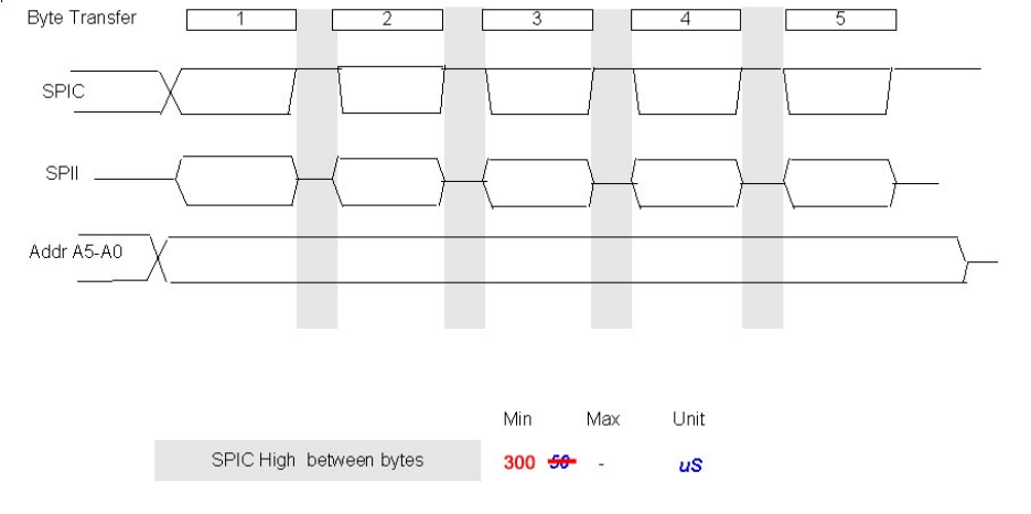
3.7.1 Power Amplifier DeviceID 0 transfer protocol
DeviceID 0 is a 5 byte transfer with the following order:
Byte 1: Temperature
Byte 2: Forward Power
Byte 3: Reflected Power
Byte 4: DC Supply Voltage
Byte 5: DC Supply Current
Power Amplifier Serial I/F Spec.
12 Version 1.62
During the 5 byte transfer, A5-A0 will not normally change.
If prior to the completion of the 5 byte transfer, the SPI address A5..A0 changes, for example
due to a host reset or error, the transfer will be halted by the PA. The next time the device ID on
the addressed PA is active, the transfer begins again starting with byte 1.
The timing diagram is shown in Figure 3-3:
0Figure 3-3
3.7.2 Power Amplifier DeviceID 1 transfer protocol
DeviceID 1 is a 1 byte transfer. The timing diagram for this transfer is shown in Figure 3-2.
3.7.3 Power Amplifier DeviceID 2 transfer protocol
DeviceID 2 is a 1 byte transfer. The timing diagram for this transfer is shown in Figure 3-2.
3.7.4 Power Amplifier DeviceID 3 transfer protocol
DeviceID 3 is a 1 byte transfer. The timing diagram for this transfer is shown in Figure 3-2.
3.7.5 Power Amplifier DeviceID 4 transfer protocol
3.7.5.1 Read
A read of DeviceID 4 is a 6 byte transfer with the following order:
Byte 1: 0x03 (this is the READ instruction byte for the EEPROM)
Byte 2: target EEPROM page number (0-63) shifted left two bits (e.g page 3 = 00001100b)
Byte 3: byte 1
Byte 4: byte 2
Power Amplifier Serial I/F Spec.
13 Version 1.62
Byte 5: byte 3
Byte 6: byte 4
The timing diagram for this transfer is approximately shown in Figure 3-3, with the addition of a
byte.
3.7.5.2 Write
A write to DeviceID 4 is an 8 byte transfer with the following order:
Byte 1: 0x06 (this is the WRITE ENABLE instruction byte for the EEPROM)
Byte 2: 0x02 (this is the WRITE instruction byte for the EEPROM)
Byte 3: target EEPROM page number (0-63) shifted left two bits (e.g page 63 = 11111100b)
Byte 4: byte 1
Byte 5: byte 2
Byte 6: byte 3
Byte 7: byte 4
Byte 8: 0x04 (this is the WRITE DISABLE instruction byte for the EEPROM)
The timing diagram for this transfer is approximately shown in Figure 3-3, with the addition of 3
bytes.