WIRELESS TAG TECHNOLOGY WT32-S1 WT32-S1 WiFi/BT Module User Manual
WIRELESS-TAG TECHNOLOGY CO., LIMITED WT32-S1 WiFi/BT Module
User Manual

WT32-S1 WiFi/BT Module
e
Extreme / Open / Small / Easy
Specification
Version 1.0
2017/12/13

WT32-S1 WiFi/BT Module
WiFi/BT DATASHEET
Wireless-Tag Technology Co.,Limited
http://www.wireless-tag.com
-2-
D
is
cla
im
er
an
d
C
opy
ri
gh
t
N
ot
ice
Information in this document, including URL references, is subject to change without notice.
THIS DOCUMENT IS PROVIDED AS IS WITH NO WARRANTIES WHATSOEVER, INCLUDING ANYWARRANTY OF
MERCHANTABILITY, NON-INFRINGEMENT, FITNESS FOR ANY PARTICULARPURPOSE, OR ANY WARRANTY
OTHERWISE ARISING OUT OF ANY PROPOSAL, SPECIFICATIONOR SAMPLE. All liability, including liability for
infringement of any proprietary rights, relating to useof information in this document is disclaimed. No licenses
express or implied, by estoppel orotherwise, to any intellectual property rights are granted herein.
The WiFi Alliance Member Logo is a trademark of the WiFi Alliance.
All trade names, trademarks and registered trademarks mentioned in this document are property oftheir
respective owners, and are hereby acknowledged.
Note
As the product upgrade or other reasons, this manual may change. Shenzhen Wireless-Tag Technology Co.,
Ltd has right to modify the contents of this manual without any notice or warning. This manual is only as a
guide,Wireless-Tag Technology Co., Ltd Spareno effort to provide accurate information in this manual, but the
Wireless-Tag can't guarantee manual there is no problem , all statements in this manual, information and
suggestions do not constitute any guarantee of express or implication.


WT32-S1 WiFi/BT Module
WiFi/BT DATASHEET
Wireless-Tag Technology Co.,Limited
http://www.wireless-tag.com
-4-
Contents
1.Overview....................................................................................................................................................... - 5 -
2. Main Features.............................................................................................................................................. - 5 -
3.HardwareSpecifications..............................................................................................................................- 7-
3.1 Pin Description....................................................................................................................................... - 7 -
3.1.1StrappingPins.....................................................................................................................................- 8 -
3.2 Functional Description............................................................................................................................. - 10 -
3.2.1 CPU and Internal Memory................................................................................................................ - 10 -
3.2.2 Low-Power Management.................................................................................................................- 10 -
Note:...................................................................................................................................................... - 11 -
3.3 Peripherals and Sensors .......................................................................................................................... - 12 -
3.4Electrical Characteristic ........................................................................................................................ - 16 -
3.4.1Maximum Ratings.......................................................................................................................... - 16 -
3.4.2Recommended Operating Environment ....................................................................................... - 17 -
3.4.3DigitalPortCharacteristics............................................................................................................-17-
3.5RFCharacteristics................................................................................................................................- 17-
3.5.1 Wi-Fi Radio.................................................................................................................................... - 17 -
3.5.2BLERadio......................................................................................................................................-18 -
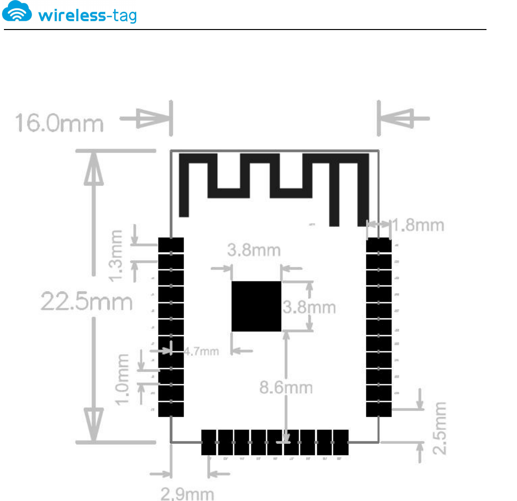
4. Mechanical Dimensions............................................................................................................................. - 19 -
4.1Module Size .......................................................................................................................................... - 19-
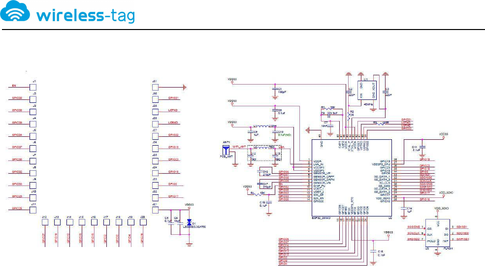
4.2 Schematics........................................................................................................................................... - 20 -
5. Product Trial........................................................................................................................................ - 20 -
WT32-S1 WiFi/BT Module
WiFi/BT DATASHEET
Wireless-Tag Technology Co.,Limited
http://www.wireless-tag.com
-5-
1.Overview
WT32-S1 WiFi/BT Module WiFi/BT Module is designed by Wireless-Tag, low consumption, cost-
effective embedded wireless network control module. It can meet the IoT application requirements in the
smart power grids, building automation, security and protection, smart home, remote health care etc.
The module's core processor is the ESP32,that is a single-chip solution that integrates dual-mode 2.4 GHz Wi-
Fi and Bluetooth in a smaller package size, using TSMC's ultra-low power 40-nanometer process with an
integrated antenna switch , RF Balun, power amplifier, low noise amplifier, filter and power management module.
ESP32 also integrates a wealth of peripherals, including capacitive touch sensors, Hall sensors, low-noise sense
amplifier, SD card interface, Ethernet interface, high-speed SDIO / SPI, UART, I2S and I2C.
ESP32 chip integrates traditional Bluetooth, Bluetooth low energy and Wi-Fi, has a wide range of uses: Wi-Fi
supports a wide range of communication connections, also supports direct connection to the Internet through a
router; and Bluetooth allows users to connect mobile phones or broadcast BLE Beacon for signal detection. ESP32
chip sleep current less than 5μA, making it suitable for battery-powered wearable electronic devices. ESP32's
operating system is freeRTOS with LWIP, and built-in TLS 1.2 with hardware acceleration. The chip also supports
OTA encryption upgrade, developers can continue to upgrade after the release of the product.
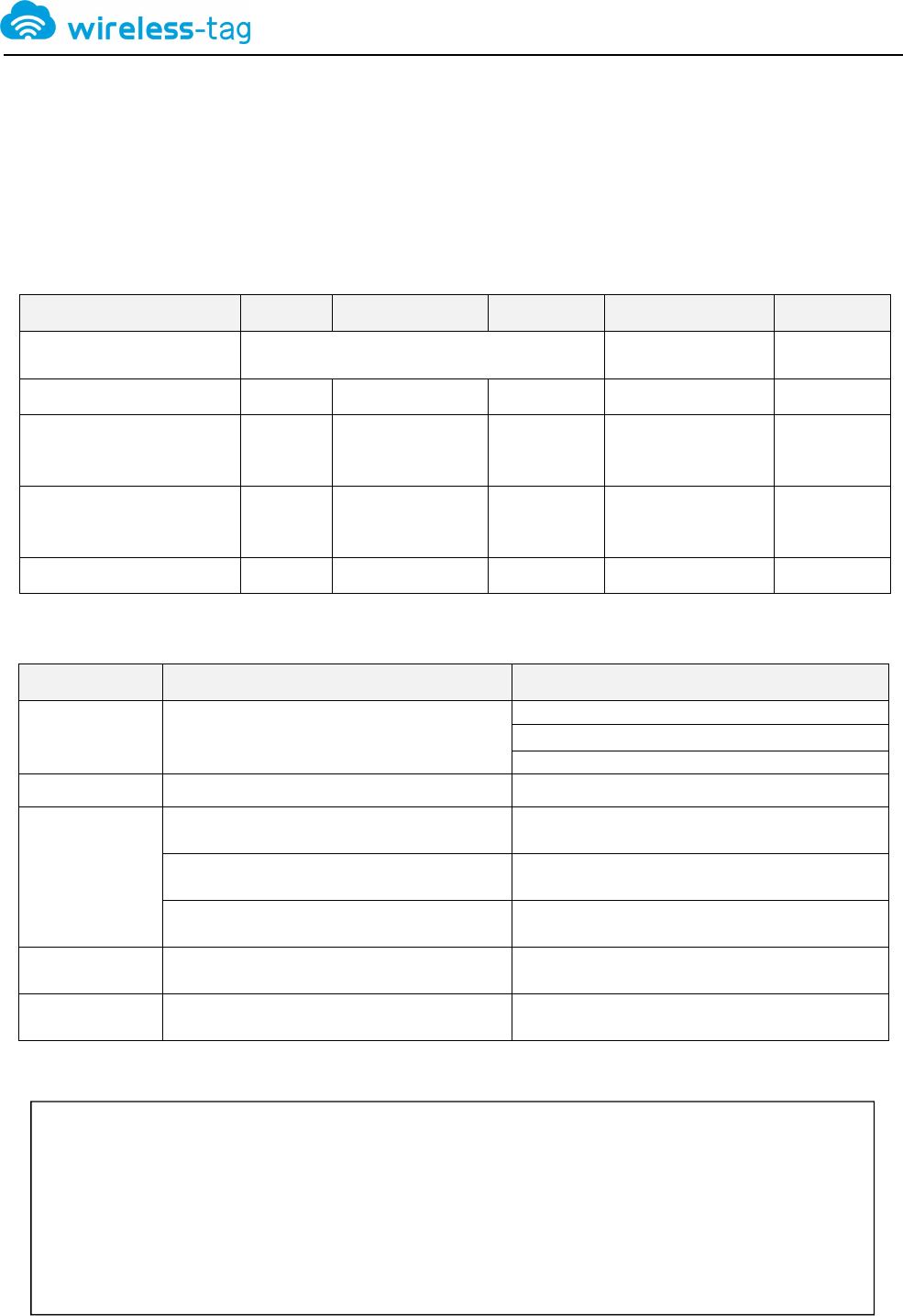
2. Main Features
WT32-S1 WiFi/BT Module Specifications Table 1
Table-1 Specifications
Categories
Items
Specifications
Wi-Fi
RF certification
FCC/CE/RoHS
Protocols
802.11 b/g/n/e/i (802.11n up to 150 Mbps)
A-MPDU and A-MSDU aggregation and 0.4
μ
s guard interval support
Frequency range
2.4~2.5 GHz
Bluetooth
Protocols
Bluetooth v4.2 BLE specification
Radio
NZIF receiver with -97 dBm sensitivity
Class-1, class-2 and class-3 transmitter
AFH
Audio
CVSD and SBC
Hardware
Module interface
SD card, UART, SPI, SDIO, I2C, LED PWM,
Motor PWM, I2S, IR
GPIO, capacitive touch sensor, ADC, DAC,
LNA preamplifier
On-chip sensor
Hall sensor, temperature sensor
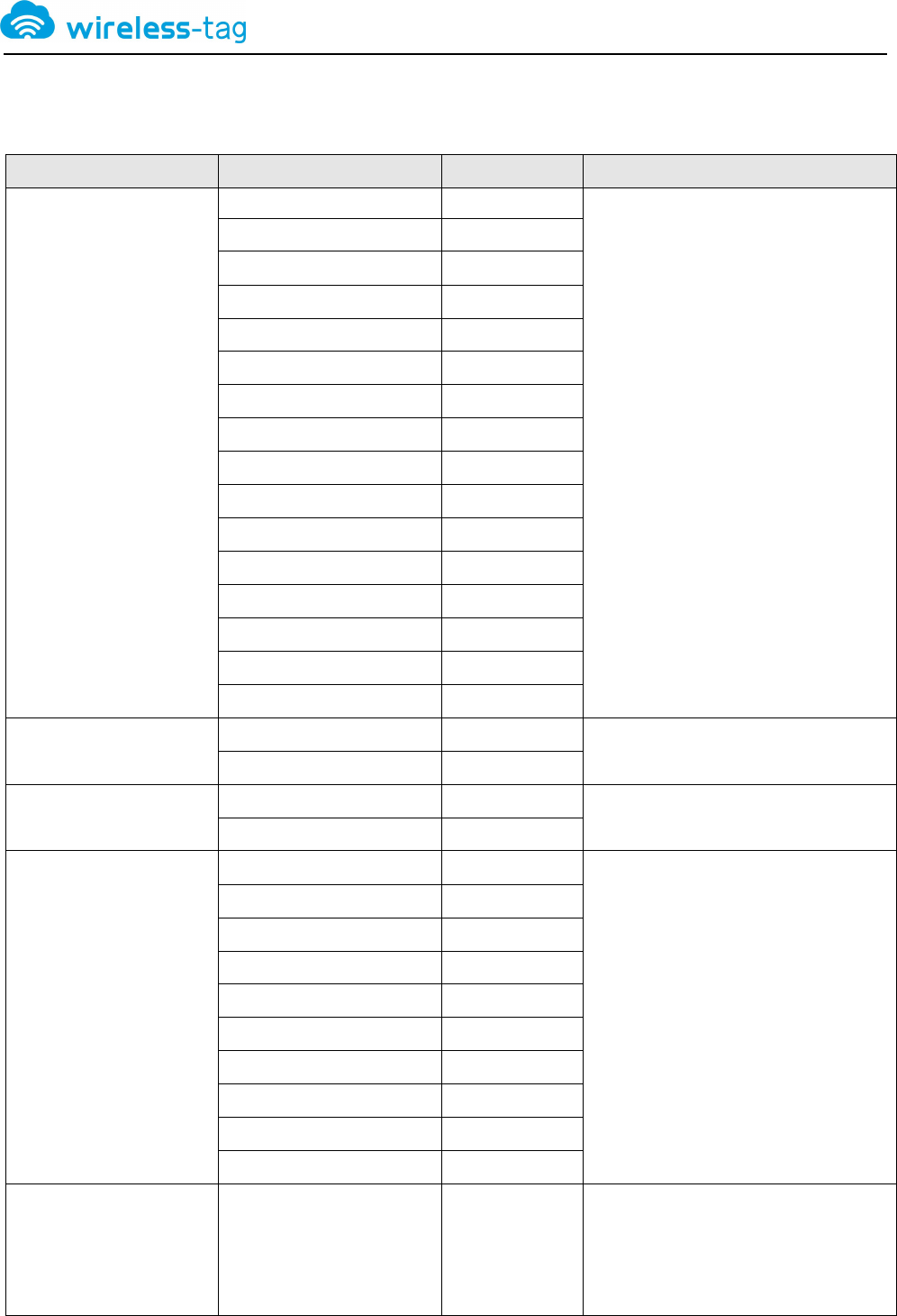
WT32-S1 WiFi/BT Module
WiFi/BT DATASHEET
Wireless-Tag Technology Co.,Limited
http://www.wireless-tag.com
-6-
On-board clock
40 MHz crystal
Operating voltage/Power supply
2.7~3.6V
Operating current
Average: 80 mA
Minimum current delivered by
power supply
500 mA
Operating temperature range
-40°C~+85°C
Ambient temperature range
Normal temperature
Package size
22.5mm x16mm x3.7mm
Software
Wi-Fi mode
Station/softAP/SoftAP+station/P2P
Wi-Fi Security
WPA/WPA2/WPA2-Enterprise/WPS
Encryption
AES/RSA/ECC/SHA
Firmware upgrade
UART Download / OTA (download and write
firmware via network or host)
Software development
Supports Cloud Server Development / SDK
for custom firmware development
Network protocols
IPv4,IPv6,SSL,TCP/UDP/HTTP/FTP/MQTT
User configuration
AT instruction set, cloud server, Android/iOS
app
WT32-S1 WiFi/BT Module
WiFi/BT DATASHEET
Wireless-Tag Technology Co.,Limited
http://www.wireless-tag.com
-7-
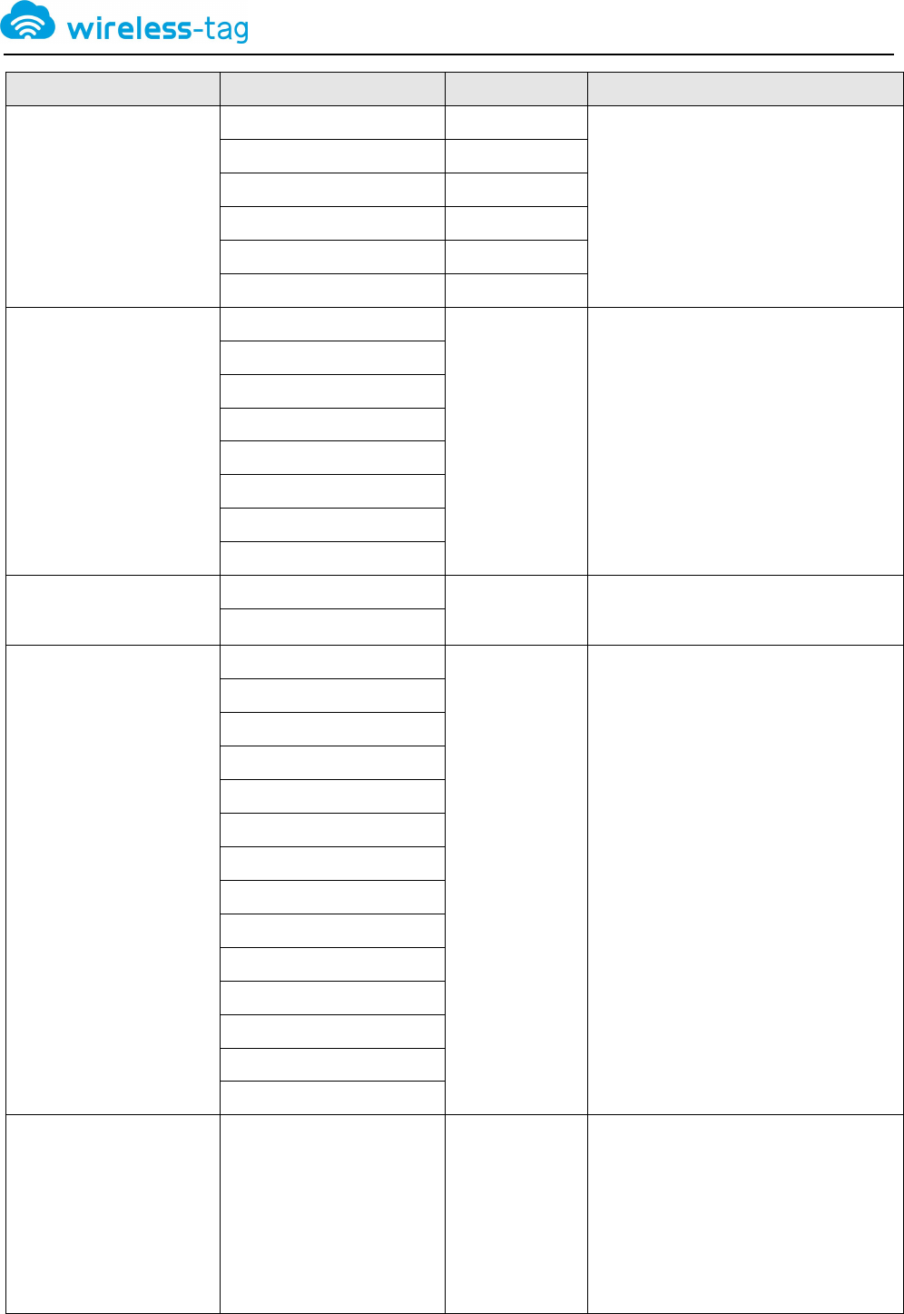
3. Hardware Specifications
3.1 Pin Description
Figure-1 WT32-S1 WiFi/BT Module
Pinout (Bottom View) Table-2 Pin
Definition and Description
No.
Name
Function
1
EN
Chip-enable signal. Active high.
2
IO36
GPI36, SENSOR_VP, ADC_H, ADC1_CH0, RTC_GPIO0
3
IO38
GPI38, SENSOR_CAPN, ADC_H, ADC1_CH2, RTC_GPIO2

http://www.wireless-tag.com
-8-
WT32-S1 WiFi/BT Module
WiFi/BT DATASHEET
Wireless-Tag Technology Co.,Limited
4
IO39
GPI39, SENSOR_VN, ADC_H, ADC1_CH3, RTC_GPIO3
5
IO34
GPI34, ADC1_CH6, RTC_GPIO4
6
IO37
GPI37, SENSOR_CAPP, ADC_H, ADC1_CH1, RTC_GPIO1
7
IO35
GPI35, ADC1_CH7, RTC_GPIO5
8
IO32
GPIO32, XTAL_32K_P (32.768 kHz crystal oscillator input),
ADC1_CH4, TOUCH9, RTC_GPIO9
9
IO33
GPIO33, XTAL_32K_N (32.768 kHz crystal oscillator output),
ADC1_CH5, TOUCH8, RTC_GPIO8
10
IO25
GPIO25, DAC_1, ADC2_CH8, RTC_GPIO6, EMAC_RXD0
11
IO26
GPIO26, DAC_2, ADC2_CH9, RTC_GPIO7, EMAC_RXD1
12
IO27
GPIO27, ADC2_CH7, TOUCH7, RTC_GPIO17,
EMAC_RX_DV
13
IO14
GPIO14, ADC2_CH6, TOUCH6, RTC_GPIO16, MTMS,
HSPICLK, HS2_CLK, SD_CLK, EMAC_TXD2
14
IO12
GPIO12, ADC2_CH5, TOUCH5, RTC_GPIO15, MTDI,
HSPIQ, HS2_DATA2, SD_DATA2, EMAC_TXD3
15
IO13
GPIO13, ADC2_CH4, TOUCH4, RTC_GPIO14, MTCK,
HSPID, HS2_DATA3, SD_DATA3, EMAC_RX_ER
16
IO15
GPIO15, ADC2_CH3, TOUCH3, MTDO, HSPICS0,
RTC_GPIO13, HS2_CMD, SD_CMD, EMAC_RXD3
17
IO2
GPIO2, ADC2_CH2, TOUCH2, RTC_GPIO12, HSPIWP,
HS2_DATA0, SD_DATA0
18
IO0
GPIO0, ADC2_CH1, TOUCH1, RTC_GPIO11, CLK_OUT1,
EMAC_TX_CLK
19
IO4
GPIO4, ADC2_CH0, TOUCH0, RTC_GPIO10, HSPIHD,
HS2_DATA1, SD_DATA1, EMAC_TX_ER
20
IO16
GPIO16, HS1_DATA4, U2RXD, EMAC_CLK_OUT
21
3V3
Power supply.
22
IO17
GPIO17, HS1_DATA5, U2TXD, EMAC_CLK_OUT_180
23
IO5
GPIO5, VSPICS0, HS1_DATA6, EMAC_RX_CLK
24
IO18
GPIO18, VSPICLK, HS1_DATA7
25
IO23
GPIO23, VSPID, HS1_STROBE
26
IO19
GPIO19, VSPIQ, U0CTS, EMAC_TXD0
27
IO22
GPIO22, VSPIWP, U0RTS, EMAC_TXD1
28
U0RXD
GPIO3, U0RXD, CLK_OUT2
29
U0TXD
GPIO1, U0TXD, CLK_OUT3, EMAC_RXD2
30
IO21
GPIO21, VSPIHD, EMAC_TX_EN
31
GND
Ground
3.1.1 Strapping Pins
ESP32 has five strapping pins, which can be seen in Section 6 Schematics:
•MTDI
WT32-S1 WiFi/BT Module
WiFi/BT DATASHEET
Wireless-Tag Technology Co.,Limited
http://www.wireless-tag.com
-9-
•GPIO0
•GPIO2
•MTDO
•GPIO5
Software can read the value of these five bits from the register "GPIO_STRAPPING".
During the chip's system reset (power-on reset, RTC watchdog reset and brownout reset), the latches of the
strapping pins sample the voltage level as strapping bits of "0" or "1", and hold these bits until the chip is powered
down or shut down. The strapping bits configure the device boot mode, the operating voltage of VDD_SDIO and
other system initial settings.
Each strapping pin is connected with its internal pull-up/pull-down during the chip reset. Consequently, if a
strapping pin is unconnected or the connected external circuit is high-impendence, the internal weak pull-up/pull-
down will determine the default input level of the strapping pins.
To change the strapping bit values, users can apply the external pull-down/pull-up resistances, or apply the
host MCU's GPIOs to control the voltage level of these pins when powering on ESP32.
After reset, the strapping pins work as the normal functions pins.
Refer to Table 3 for detailed boot modes'configuration by strapping pins.
Table-3 Strapping Pins
Voltage of Internal LDO (VDD_SDIO)
Pin
Default
3.3V
1.8V
MTDI/GPIO12
Pull-down
0
1
Booting Mode
Pin
Default
SPI Boot
Download Boot
GPIO0
Pull-up
1
0
GPIO2
Pull-down
Don't-care
0
Debugging Log on U0TXD During Booting
Pin
Default
U0TXD Toggling
U0TXD Silent
MTDO/GPIO15
Pull-up
1
0
Timing of SDIO Slave
Pin
Default
Falling-edge Input
Falling-edge Output
Falling-edge Input
Rising-edge Output
Rising-edge Input
Falling-edge Output
Rising-edge Input
Rising-edge Output
MTDO
Pull-up
0
0
1
1
GPIO5
Pull-up
0
1
0
1

WT32-S1 WiFi/BT Module
WiFi/BT DATASHEET
Wireless-Tag Technology Co.,Limited
http://www.wireless-tag.com
-10 -
3.2 Functional Description
3.2.1 CPU and Internal Memory
ESP32-D0WDQ6 contains two low-power Xtensa® 32-bit LX6 microprocessors. The internal memory includes:
•448 kB of ROM for booting and core functions.
•520 kB (8 kB RTC FAST Memory included) of on-chip SRAM for data and instruction.
•8 kB of SRAM in RTC, which is called RTC FAST Memory and can be used for data storage; it is accessed
by the main CPU during RTC Boot from the Deep-sleep mode.
•8 kB of SRAM in RTC, which is called RTC SLOW Memory and can be accessed by the co-processor during
the Deep-sleep mode.
•1 kbit of eFuse, of which 256 bits are used for the system (MAC address and chip configuration) and the
remaining 768 bits are reserved for customer applications, including Flash-Encryption and Chip-ID.
3.2.2 Low-Power Management
With the use of advanced power management technologies, ESP32 can switch between different power
modes.
•
Power modes
–Active mode: The chip radio is powered on. The chip can receive, transmit, or listen.
–Modem-sleep mode: The CPU is operational and the clock is configurable. The Wi-Fi/Bluetooth baseband
and radio are disabled.
–Light-sleep mode: The CPU is paused. The RTC memory and RTC peripherals, as well as the ULP
co-processor are running. Any wake-up events (MAC, host, RTC timer, or external interrupts) will wake
up the chip.
–Deep-sleep mode: Only the RTC memory and RTC peripherals are powered on. Wi-Fi and Bluetooth
connection data are stored in the RTC memory. The ULP co-processor can work.
–Hibernation mode: The internal 8-MHz oscillator and ULP co-processor are disabled. The RTC recovery
memory is powered down. Only one RTC timer on the slow clock and some RTC GPIOs are active.The RTC
timer or the RTC GPIOs can wake up the chip from the Hibernation mode.
•
Sleep Patterns
–Association sleep pattern: The power mode switches between the Active mode, Modem- andLightsleep
WT32-S1 WiFi/BT DATASHEET
Wireless-Tag Technology Co.,Limited
http://www.wireless-tag.com
-
11
-
Note:
•In Modem-sleep mode, the CPU frequency changes automatically. The frequency depends on the CPU
load and the peripherals used.
•During Deep-sleep, when the ULP co-processor is powered on, peripherals such as GPIO and I2C are
able to work.
•When the system works in the ULP sensor-monitored pattern, the ULP co-processor works with the
ULP sensor periodically; ADC works with a duty cycle of 1%, so the power consumption is 100 μA.
mode during this sleep pattern. The CPU, Wi-Fi, Bluetooth, and radio are woken up at predetermined
intervals to keep Wi-Fi/BT connections alive.
–ULP sensor-monitored pattern: The main CPU is in the Deep-sleep mode. The ULP co-processor takes
sensor measurements and wakes up the main system, based on the data collected from sensors.
Table-4 Functionalities Depending on the Power Modes
Power mode
Active
Modem-sleep
Light-sleep
Deep-sleep
Hibernation
Sleep mode
Association sleep pattern
ULP sensor-
monitored pattern
-
CPU
ON
ON
PAUSE
OFF
OFF
Wi-Fi/BT baseband and
radio
ON
OFF
OFF
OFF
OFF
RTC memory and RTC
peripherals
ON
ON
ON
ON
OFF
ULP co-processor
ON
ON
ON
ON /OFF
OFF
Table-5 Power Consumption by Power Modes
Power mode
Description
Power consumption
Modem-sleep
The CPU is powered on.
Max speed 240 MHz: 30 mA ~ 50 mA
Normal speed 80 MHz: 20 mA ~ 25 mA
Slow speed 2 MHz: 2 mA ~ 4 mA
Light-sleep
-
0.8 mA
Deep-sleep
The ULP co-processor is powered on.
150
μ
A
ULP sensor-monitored pattern
100
μ
A @1% duty
RTC timer + RTC memory
10
μ
A
Hibernation
RTC timer only
5
μ
A
Power off
CHIP_PU is set to low level, the chip
is powered off
0.1
μ
A
WT32-S1 WiFi/BT DATASHEET
Wireless-Tag Technology Co.,Limited
http://www.wireless-tag.com
-
12
-
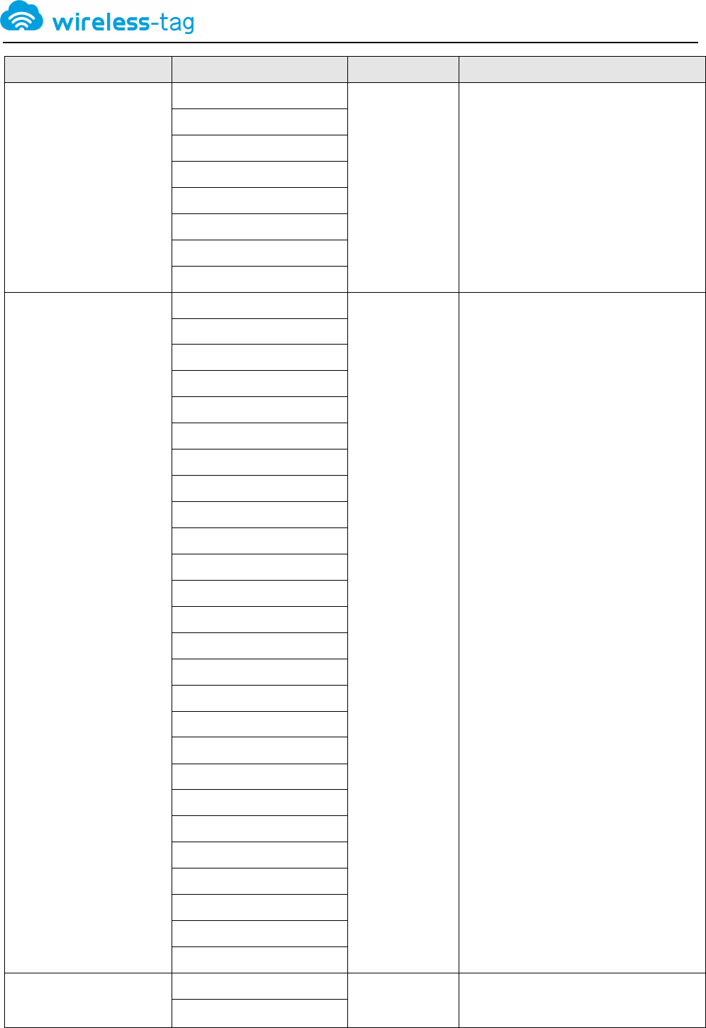
3.3 Peripherals and Sensors
Table-6 Description of Peripherals and Sensors
Interface
Signal
Pin
Function
ADC
ADC1_CH0
SENSOR_VP
Two 12-bit SAR ADCs
ADC1_CH3
SENSOR_VN
ADC1_CH4
IO32
ADC1_CH5
IO33
ADC1_CH6
IO34
ADC1_CH7
IO35
ADC2_CH0
IO4
ADC2_CH1
IO0
ADC2_CH2
IO2
ADC2_CH3
IO15
ADC2_CH4
IO13
ADC2_CH5
IO12
ADC2_CH6
IO14
ADC2_CH7
IO27
ADC2_CH8
IO25
ADC2_CH9
IO26
Ultra-Low Noise
Analog Pre-Amplifier
SENSOR_VP
IO36
Provides about 60 dB gain by
using larger capacitors on PCB
SENSOR_VN
IO39
DAC
DAC_1
IO25
Two 8-bit DACs
DAC_2
IO26
Touch Sensor
TOUCH0
IO4
Capacitive touch sensors
TOUCH1
IO0
TOUCH2
IO2
TOUCH3
IO15
TOUCH4
IO13
TOUCH5
IO12
TOUCH6
IO14
TOUCH7
IO27
TOUCH8
IO33
TOUCH9
IO32
WT32-S1 WiFi/BT DATASHEET
Wireless-Tag Technology Co.,Limited
http://www.wireless-tag.com
-
13
-
Interface
Signal
Pin
Function
SD/SDIO/MMC Host
Controller
HS2_CLK
MTMS
Supports SD memory card V3.01
standard
HS2_CMD
MTDO
HS2_DATA0
IO2
HS2_DATA1
IO4
HS2_DATA2
MTDI
HS2_DATA3
MTCK
Motor PWM
PWM0_OUT0~2
Any GPIOs
Three channels of 16-bit timers
generate PWM waveforms. Each
channel has a pair of output
signals, three fault detection
signals, three event-capture
signals, and three sync signals.
PWM1_OUT_IN0~2
PWM0_FLT_IN0~2
PWM1_FLT_IN0~2
PWM0_CAP_IN0~2
PWM1_CAP_IN0~2
PWM0_SYNC_IN0~2
PWM1_SYNC_IN0~2
LED PWM
ledc_hs_sig_out0~7
Any GPIOs
16 independent channels @80
MHz clock/RTC CLK. Duty
accuracy: 16 bits.
ledc_ls_sig_out0~7
UART
U0RXD_in
Any GPIOs
Two UART devices with
hardware flow-control and DMA
U0CTS_in
U0DSR_in
U0TXD_out
U0RTS_out
U0DTR_out
U1RXD_in
U1CTS_in
U1TXD_out
U1RTS_out
U2RXD_in
U2CTS_in
U2TXD_out
U2RTS_out
WT32-S1 WiFi/BT DATASHEET
Wireless-Tag Technology Co.,Limited
http://www.wireless-tag.com
-
14
-
Interface
Signal
Pin
Function
I2C
I2CEXT0_SCL_in
Any GPIOs
Two I2C devices in slave or
master modes
I2CEXT0_SDA_in
I2CEXT1_SCL_in
I2CEXT1_SDA_in
I2CEXT0_SCL_out
I2CEXT0_SDA_out
I2CEXT1_SCL_out
I2CEXT1_SDA_out
I2S
I2S0I_DATA_in0~15
Any GPIOs
Stereo input and output from/to
the audio codec, and parallel
LCD data output
I2S0O_BCK_in
I2S0O_WS_in
I2S0I_BCK_in
I2S0I_WS_in
I2S0I_H_SYNC
I2S0I_V_SYNC
I2S0I_H_ENABLE
I2S0O_BCK_out
I2S0O_WS_out
I2S0I_BCK_out
I2S0I_WS_out
I2S0O_DATA_out0~23
I2S1I_DATA_in0~15
I2S1O_BCK_in
I2S1O_WS_in
I2S1I_BCK_in
I2S1I_WS_in
I2S1I_H_SYNC
I2S1I_V_SYNC
I2S1I_H_ENABLE
I2S1O_BCK_out
I2S1O_WS_out
I2S1I_BCK_out
I2S1I_WS_out
I2S1O_DATA_out0~23
Remote Controller
RMT_SIG_IN0~7
Any GPIOs
Eight channels of IR transmitter
and receiver for various
waveforms
RMT_SIG_OUT0~7
WT32-S1 WiFi/BT DATASHEET
Wireless-Tag Technology Co.,Limited
http://www.wireless-tag.com
-
15
-
Interface
Signal
Pin
Function
Parallel QSPI
SPIHD
SHD/SD2
Supports Standard SPI, Dual
SPI, and Quad SPI that can be
connected to the external flash
and SRAM
SPIWP
SWP/SD3
SPICS0
SCS/CMD
SPICLK
SCK/CLK
SPIQ
SDO/SD0
SPID
SDI/SD1
HSPICLK
IO14
HSPICS0
IO15
HSPIQ
IO12
HSPID
IO13
HSPIHD
IO4
HSPIWP
IO2
VSPICLK
IO18
VSPICS0
IO5
VSPIQ
IO19
VSPID
IO23
VSPIHD
IO21
VSPIWP
IO22
General Purpose
SPI
HSPIQ_in/_out
Any GPIOs
Standard SPI consists of clock,
chip-select, MOSI and MISO.
These SPIs can be connected to
LCD and other external devices.
They support the following
features:
•both master and slave modes;
•4 sub-modes of the SPI format
transfer that depend on the
clock phase (CPHA) and clock
polarity (CPOL) control;
•configurable SPI frequency;
•up to 64 bytes of FIFO and DMA.
HSPID_in/_out
HSPICLK_in/_out
HSPI_CS0_in/_out
HSPI_CS1_out
HSPI_CS2_out
VSPIQ_in/_out
VSPID_in/_out
VSPICLK_in/_out
VSPI_CS0_in/_out
VSPI_CS1_out
VSPI_CS2_out
JTAG
MTDI
IO12
JTAG for software debugging
MTCK
IO13
MTMS
IO14
MTDO
IO15
WT32-S1 WiFi/BT Module
WiFi/BT DATASHEET
Wireless-Tag Technology Co.,Limited
http://www.wireless-tag.com
-
16
-
Interface
Signal
Pin
Function
SDIO
SD_CLK
IO6
SDIO interface that conforms to
the industry standard SDIO 2.0
card specification.
SD_CMD
IO11
SD_DATA0
IO7
SD_DATA1
IO8
SD_DATA2
IO9
SD_DATA3
IO10
EMAC
EMAC_TX_CLK
IO0
Ethernet MAC with MII/RMII
interface
EMAC_RX_CLK
IO5
EMAC_TX_EN
IO21
EMAC_TXD0
IO19
EMAC_TXD1
IO22
EMAC_TXD2
IO14
EMAC_TXD3
IO12
EMAC_RX_ER
IO13
EMAC_RX_DV
IO27
EMAC_RXD0
IO25
EMAC_RXD1
IO26
EMAC_RXD2
TXD
EMAC_RXD3
IO15
EMAC_CLK_OUT
IO16
EMAC_CLK_OUT_180
IO17
EMAC_TX_ER
IO4
EMAC_MDC_out
Any GPIO
EMAC_MDI_in
Any GPIO
EMAC_MDO_out
Any GPIO
EMAC_CRS_out
Any GPIO
EMAC_COL_out
Any GPIO
3.4 Electrical Characteristic
3.4.1 Maximum Ratings
Table-7. Maximum Ratings
Ratings
Condition
Value
Unit
Storage Temperature
/
-45 to 85
°C
Maximum Soldering
Temperature
/
245
°C
Supply Voltage
IPC/JEDEC J-STD-020
+2.7 to +3.6
V
WT32-S1 WiFi/BT Module
WiFi/BT DATASHEET
Wireless-Tag Technology Co.,Limited
http://www.wireless-tag.com
-
17
-
3.4.2 Recommended Operating Environment
Table-8 Recommended Operating Environment
Working
Environment
Name
Min Value
Typical Values
Max Value
Unit
Operating
Temperature
/
-40
20
85
°C
Supply Voltage
VDD
2.7
3.3
3.6
V
3.4.3 Digital Port Characteristics
Table-9 Digital Port Characteristics
Port
Typical Values
Min Value
Max Value
Unit
Input low logic level
VIL
-0.3
0.25VDD
V
Input high logic level
VIH
0.75vdd
VDD+0.3
V
Output low logic level
VOL
N
0.1VDD
V
Output high logic level
VOL
0.8VDD
N
V
3.5 RF Characteristics
3.5.1 Wi-Fi Radio
Table-10 Wi-Fi Radio Characteristics
Description
Min
Typical
Max
Unit
Input frequency
2412
-
2484
MHz
Input reflection
-
-
-10
dB
Sensitivity
DSSS, 1 Mbps
-
-98
-
dBm
CCK, 11 Mbps
-
-90
-
dBm
OFDM, 6 Mbps
-
-93
-
dBm
OFDM, 54 Mbps
-
-75
-
dBm
HT20, MCSO
-
-93
-
dBm
HT20, MCS7
-
-73
-
dBm
HT40, MCSO
-
-90
-
dBm
HT40, MCS7
-
-70
-
dBm
MCS32
-
-91
-
dBm
Adjacent channel rejection
OFDM, 6 Mbps
-
37
-
dB
OFDM, 54 Mbps
-
21
-
dB
HT20, MCS0
-
37
-
dB
HT20, MCS7
-
20
-
dB
WT32-S1 WiFi/BT Module
WiFi/BT DATASHEET
Wireless-Tag Technology Co.,Limited
http://www.wireless-tag.com
-
18
-
3.5.2 BLE Radio
Table-11 Receiver Characteristics —BLE
Parameter
Conditions
Min
Typ
Max
Unit
Sensitivity @30.8% PER
-
-
-98
-
dBm
Maximum received signal
@30.8% PER
-
0
-
-
dBm
Co-channel C/I
-
-
10
-
dB
Adjacent channel selectivity
C/I
F = F0 + 1 MHz
-
-5
-
dB
F = F0 - 1 MHz
-
-5
-
dB
F = F0 + 2 MHz
-
-25
-
dB
F = F0 - 2 MHz
-
-35
-
dB
F = F0 + 3 MHz
-
-25
-
dB
F = F0 - 3 MHz
-
-45
-
dB
Out-of-band blocking
performance
30 MHz - 2000 MHz
-10
-
-
dBm
2000 MHz - 2400 MHz
-27
-
-
dBm
2500 MHz - 3000 MHz
-27
-
-
dBm
3000 MHz - 12.5 GHz
-10
-
-
dBm
Intermodulation
-
-36
-
-
dBm
Table-12 Transmitter Characteristics —BLE
Parameter
Conditions
Min
Typ
Max
Unit
RF transmit power
-
-
0
-
dBm
Gain control step
-
-
±3
-
dBm
RF power control range
-
-12
-
+12
dB
Adjacent channel
transmit power
F = F0 + 1 MHz
-
-14.6
-
dBm
F = F0 - 1 MHz
-
-12.7
-
dBm
F = F0 + 2 MHz
-
-44.3
-
dBm
F = F0 - 2 MHz
-
-38.7
-
dBm
F = F0 + 3 MHz
-
-49.2
-
dBm
F = F0 - 3 MHz
-
-44.7
-
dBm
F = F0 + > 3 MHz
-
-50
-
dBm
F = F0 - > 3 MHz
-
-50
-
dBm
∆f1avg
-
-
-
265
kHz
∆f2max
-
247
-
-
kHz
∆f2avg/∆f1avg
-
-
-0.92
-
-
ICFT
-
-
-10
-
kHz
Drift rate
-
-
0.7
-
kHz/50
μ
s
Drift
-
-
2
-
kHz
FCC Caution.
FCC Caution.
§ 15.19 Labelling requirements.
This device complies with part 15 of the FCC Rules. Operation is subject to the
following two conditions: (1) This device may not cause harmful interference, and (2)
this device must accept any interference received, including interference that may
cause
undesired operation.
§ 15.21 Information to user.
Any Changes or modifications not expressly approved by the party responsible for
compliance could void the user's authority to operate the equipment.
§ 15.105 Information to the user.
Note: This equipment has been tested and found to comply with the limits for a Class
B
digital device, pursuant to part 15 of the FCC Rules. These limits are designed to
provide reasonable protection against harmful interference in a residential installation.
This equipment generates uses and can radiate radio frequency energy and, if not
installed and used in accordance with the instructions, may cause harmful interference
to radio communications. However, there is no guarantee that interference will not
occur in a particular installation. If this equipment does cause harmful interference to
radio or television reception, which can be determined by turning the equipment off
and
on, the user is encouraged to try to correct the interference by one or more of the
following measures:
-Reorient or relocate the receiving antenna.
-Increase the separation between theequipment and receiver.
-Connect the equipment into an outlet on a circuit different from that to which the
receiver is connected.
-Consult the dealer or an experienced radio/TV technician for help.
The device has been evaluated to meet general RF exposure requirement.
The device can be used in portable exposure condition without restriction.