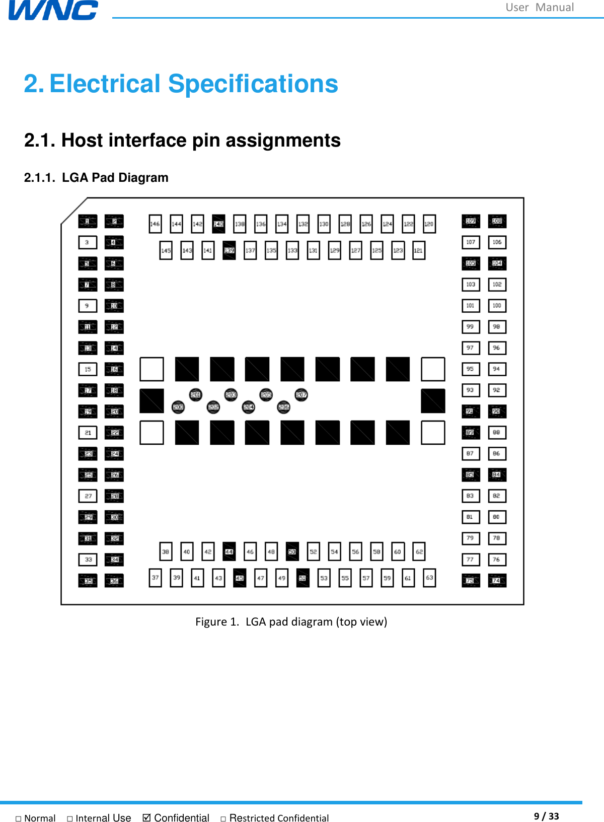
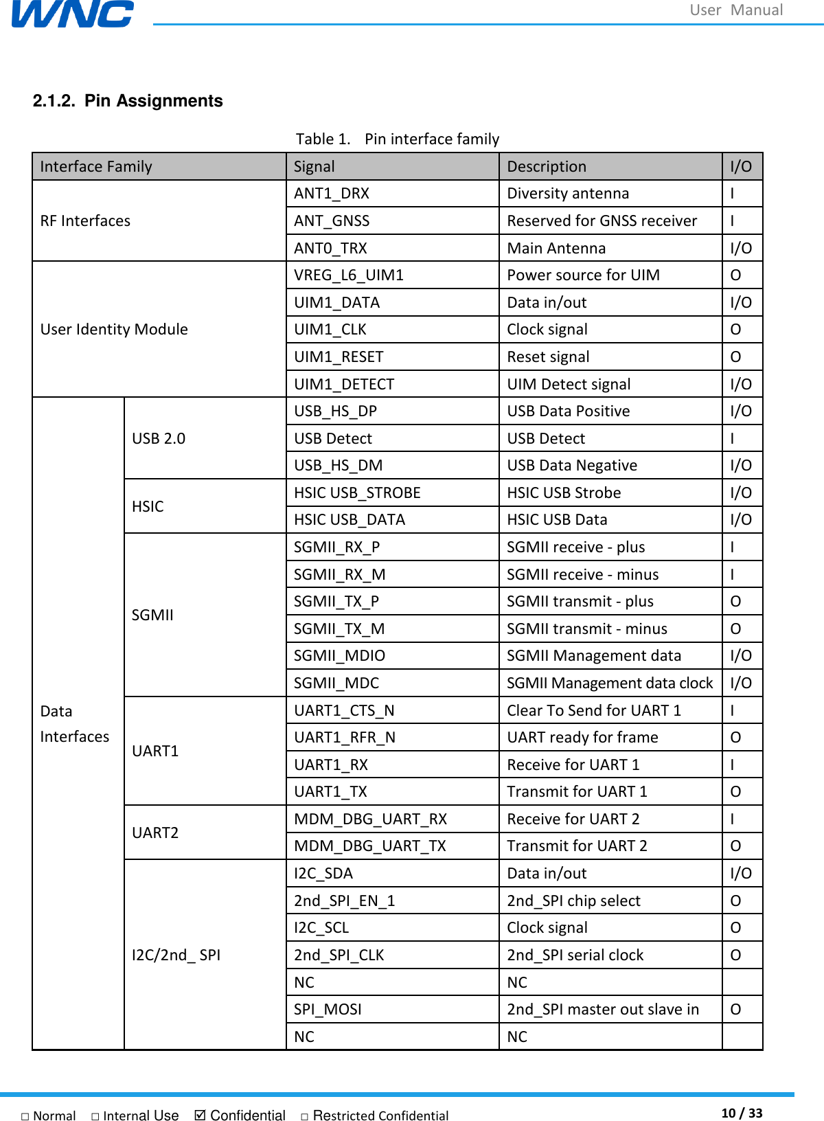
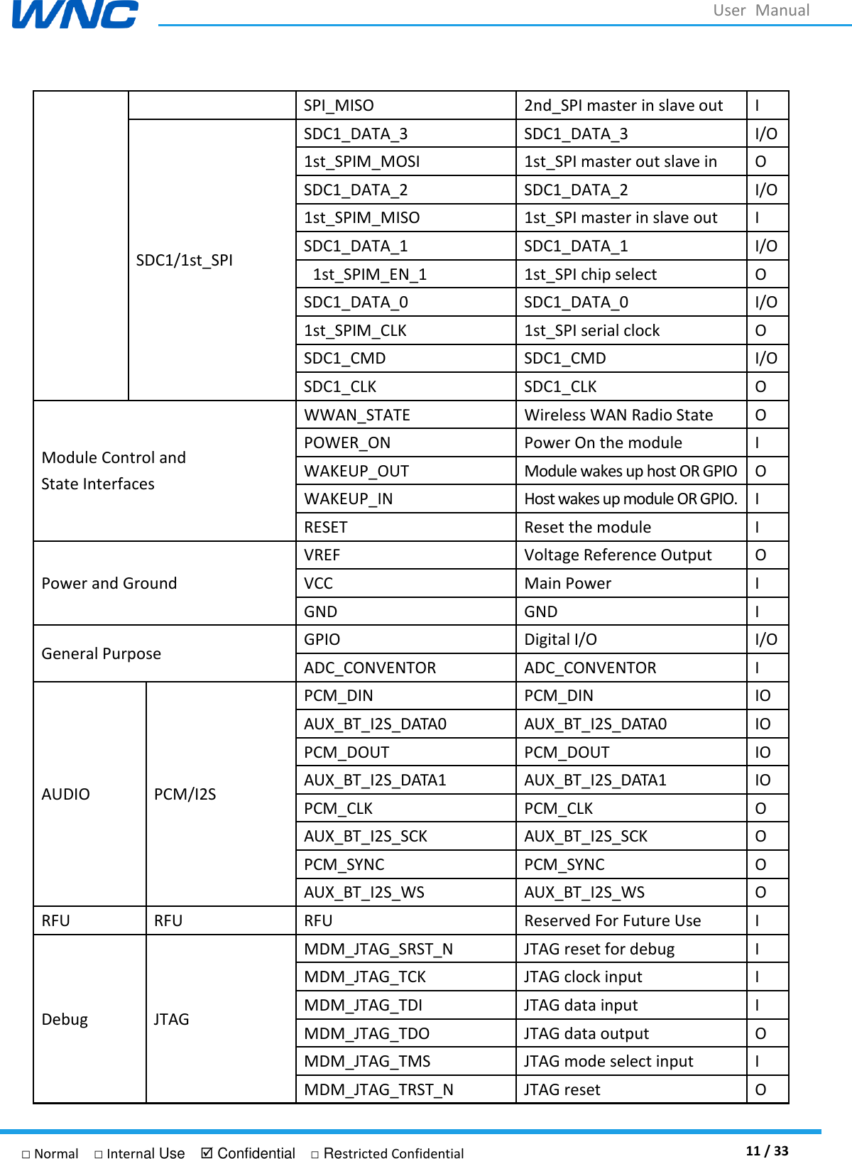
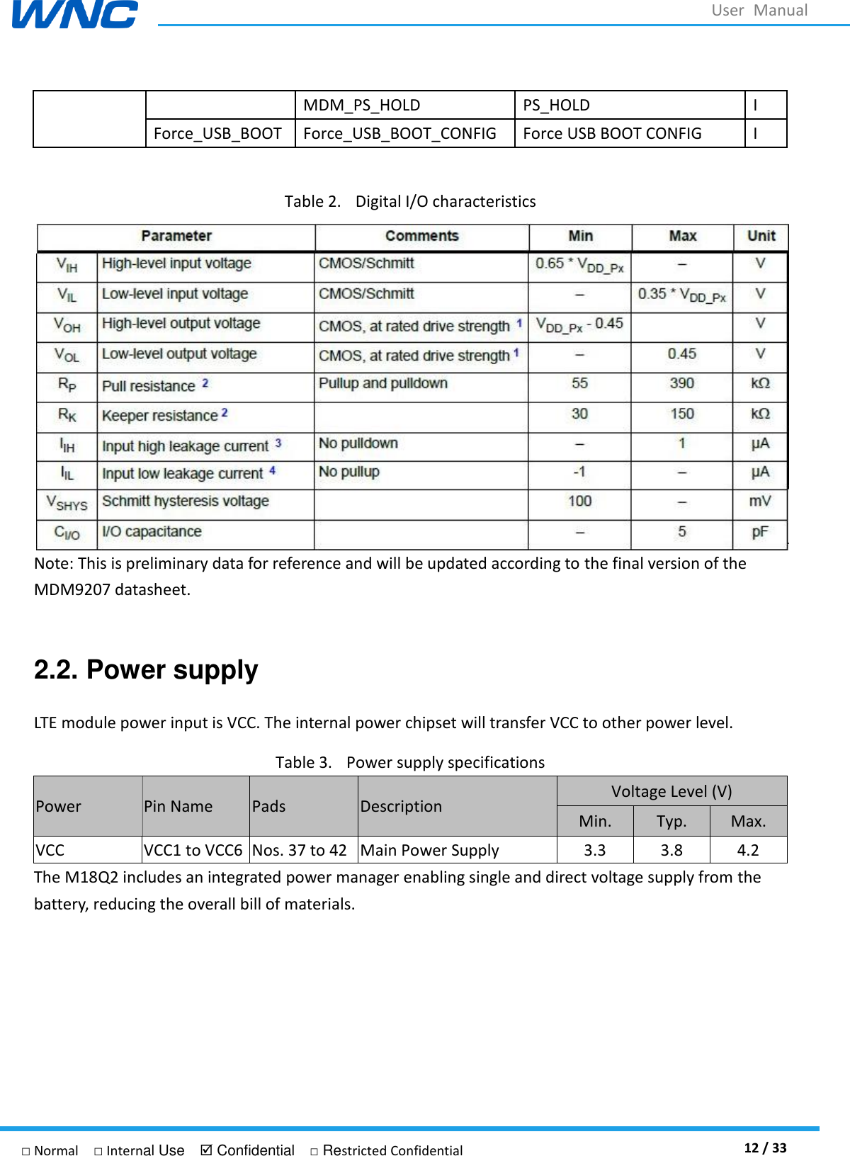
Wistron NeWeb M18Q2 LGA Module User Manual 1

Wistron NeWeb Corporation LGA Module 1

User Manual

 1 / 33 □ Normal  □ Internal Use   Confidential  □ Restricted Confidential                    User manual     Project Name: M18Q2 Author: Wistron NeWeb Corporation   Revision: 1.4 Revision Date: 2016/05/20
 2 / 33 □ Normal  □ Internal Use   Confidential  □ Restricted Confidential User  Manual Contact Information Sale and Technical Support SupportIoT.MBA@wnc.com.tw Website www.wnc.com.tw  Revision History Rev. # Author Summary of Changes Date 1.0 WNC MBU Draft release 2016/4/15 1.1 WNC MBU Fine-tune wording 2016/5/12 1.2 WNC MBU Update RF Exposure Information 2016/5/17 1.3 WNC MBU Update antenna and PCB layout guidance 2016/5/17 1.4 WNC MBU Update layout guidance   2016/5/20
 3 / 33 □ Normal  □ Internal Use   Confidential  □ Restricted Confidential User  Manual ©  Wistron NeWeb Corporation THIS DOCUMENT AND THE INFORMATION CONTAINED HEREIN IS PROPRIETARY AND IS THE EXCLUSIVE PROPERTY OF WNC AND SHALL NOT BE DISTRIBUTED, REPRODUCED, OR DISCLOSED IN WHOLE OR IN PART WITHOUT PRIOR WRITTEN PERMISSION FROM WNC.  LIMITATION OF LIABILITY THIS DOCUMENT AND THE INFORMATION CONTAINED HEREIN IS PURELY FOR DESIGN REFERENCE AND SUBJECT TO REVISION BY WNC AT ANY TIME. NOTHING IN THIS DOCUMENT SHALL BE CONSTRUED AS GRANTING ANY WARRANTY OR RIGHT TO USE THE MATERIAL CONTAINED HEREIN WITHOUT WNC’S PRIOR EXPRESS WRITTEN CONSENT. WNC SHALL NOT BE LIABLE FOR ANY USE, APPLICATION OR DEVELOPMENT DERIVED FROM THE MATERIAL WITHOUT SUCH PRIOR EXPRESS WRITTEN CONSENT. FCC Regulations: This device complies with part 15 of the FCC Rules. Operation is subject to the following two conditions: (1) This device may not cause harmful interference, and (2) This device must accept any interference received, including interference that may cause undesired operation. This device has been tested and found to comply with the limits for a Class B digital device, pursuant to Part 15 of the FCC Rules. These limits are designed to provide reasonable protection against harmful interference in a residential installation. This equipment generates, uses and can radiated radio frequency energy and, if not installed and used in accordance with the instructions, may cause harmful interference to radio communications. However, there is no guarantee that interference will not occur in a particular installation If this equipment does cause harmful interference to radio or television reception, which can be determined by turning the equipment off and on, the user is encouraged to try to correct the interference by one or more of the following measures: -Reorient or relocate the receiving antenna. -Increase the separation between the equipment and receiver. -Connect the equipment into an outlet on a circuit different from that to which the receiver is connected. -Consult the dealer or an experienced radio/TV technician for help.  Caution: Changes or modifications not expressly approved by the party responsible for compliance could void the user‘s authority to operate the equipment.
 4 / 33 □ Normal  □ Internal Use   Confidential  □ Restricted Confidential User  Manual RF Exposure Information This device is intended only for OEM integrators under the following conditions:  (1) The antenna must be installed such that 20 cm is maintained between the antenna and users,  (2) The transmitter module may not be co-located with any other transmitter or antenna.  (3) To comply with FCC regulations limiting both maximum RF output power and human exposure to RF radiation, the maximum antenna gain including cable loss in a mobile exposure condition must not exceed:    Standalone Condition:  。 8.0 dBi in 700 MHz Band    。8.0 dBi in 850 MHz Band   。5.0 dBi in 1700 MHz Band   。7.5 dBi in 1900 MHz Band Assuming collocated with a WLAN transmitter with maximum 27 dBm average EIRP power  。 7.0 dBi in 700 MHz Band   。5.0 dBi in 850 MHz Band   。5.0 dBi in 1700 MHz Band   。7.5 dBi in 1900 MHz Band Remark: This assumption is not valid if the output power of the collocated WLAN transmitter is higher than 27 dBm.  IMPORTANT NOTE: This module is intended for OEM integrator. The OEM integrator is still responsible for the FCC compliance requirement of the end product, which integrates this module. 20cm minimum distance has to be able to be maintained between the antenna and the users for the host this module is integrated into. Under such configuration, the FCC radiation exposure limits set forth for an population/uncontrolled environment can be satisfied. Any changes or modifications not expressly approved by the manufacturer could void the user's authority to operate this equipment. USERS MANUAL OF THE END PRODUCT: In the users manual of the end product, the end user has to be informed to keep at least 20cm separation with the antenna while this end product is installed and operated. The end user has to be informed that the FCC radio-frequency exposure guidelines for an uncontrolled environment can be satisfied. The end user has to also be informed that any changes or modifications not expressly approved by the manufacturer could void the user's authority to operate this equipment. If the size of the end product is smaller than 8x10cm, then additional FCC part 15.19 statement is required
 5 / 33 □ Normal  □ Internal Use   Confidential  □ Restricted Confidential User  Manual to be available in the users manual: This device complies with Part 15 of FCC rules. Operation is subject to the following two conditions: (1) this device may not cause harmful interference and (2) this device must accept any interference received, including interference that may cause undesired operation.
 6 / 33 □ Normal  □ Internal Use   Confidential  □ Restricted Confidential User  Manual Contents Contact Information ......................................................................................................................... 2 Revision History ................................................................................................................................ 2 Contents ........................................................................................................................................ 6 1. Introduction ........................................................................................................................... 8 1.1. Features .................................................................................................................................8 2. Electrical Specifications...................................................................................................... 9 2.1. Host interface pin assignments...........................................................................................9 2.1.1. LGA Pad Diagram ....................................................................................................9 2.1.2. Pin Assignments .....................................................................................................10 2.2. Power supply .......................................................................................................................12 2.3. USB interface .......................................................................................................................14 2.4. SGMII interface ...................................................................................................................15 2.5. HSIC interface .....................................................................................................................16 2.6. SIM interface ........................................................................................................................17 2.7. Control interface (wakeup) ................................................................................................17 2.8. Digital interface ....................................................................................................................18 2.8.1. JTAG Interface ........................................................................................................18 2.8.2. SPI Master Interface ..............................................................................................18 2.8.3. PCM Interface .........................................................................................................19 2.8.4. I2S Interface ............................................................................................................19 2.8.5. I2C Interface ...........................................................................................................20 2.8.6. UART Interface .......................................................................................................20 2.8.7. ADC Interface .........................................................................................................21 3. RF Specifications ............................................................................................................... 22 3.1. RF connections ...................................................................................................................22
 7 / 33 □ Normal  □ Internal Use   Confidential  □ Restricted Confidential User  Manual 3.2. RF Layout guidance ...........................................................................................................22 3.3. Antenna Guidance ..............................................................................................................24 3.4. Interference and sensitivity ................................................................................................24 3.5. Radiated sensitivity measurement ...................................................................................25 3.6. GNSS external circuit design ............................................................................................25 3.7. Supported frequencies .......................................................................................................25 4. Software Interface .............................................................................................................. 27 4.1. Support tools ........................................................................................................................27 4.2. USB interface .......................................................................................................................27 5. Mechanical and Environmental Certifications ............................................................... 28 5.1. PCBA Form Factor ..............................................................................................................28 5.2. Labeling ................................................................................................................................31 6. Regulatory Compliance and Certification....................................................................... 32 6.1. Certification testing .............................................................................................................32 7. Safety Recommendation ................................................................................................... 33
 8 / 33 □ Normal  □ Internal Use   Confidential  □ Restricted Confidential User  Manual 1. Introduction The M18Q2 is a Cat. 4 LTE modem which incorporates an application CPU subsystem and a host of peripheral interfaces and functions uniquely designed to address the power/performance/cost requirements of IoT and M2M applications. The chip is based on Qualcomm’s MDM architecture which offers OFDMA-related software based signal processing capabilities that significantly exceed traditional communications ARM cores.   The CPU subsystem features a high performance Cortex A7 microprocessor running a Linux OS with a variety of host interfaces including USB 2.0, SGMII, SPI, UART, PCM, I2C, HSIC, USIM & SDC. The module supports integrated VoLTE functionality, with a variety of narrow- and wide-band CODECs and full IMS signaling.  1.1. Features  3GPP category support: LTE Cat. 4 with 150/50 Mbps for DL/UL  Supports LTE B2/4/5/12  Supports WCDMA B2/5  Ultra-high-performance Cortex A7 microprocessor    Modem subsystem (MSS)  Integrated support for VoLTE  Resource and power management (RPM) subsystem  Optimized for M2M and IoT markets    Interfaces   – HS USB 2.0 with integrated PHY – SGMII interface   – HSIC interface – Dual UART interfaces (4 bit and 2 bit) for data transfer and diagnostic tools – SDC1: First SPI interface – I2C: Second SPI interface – USIM interface   – GPIOs – ADC   – PCM/I2S – JTAG interface
 9 / 33 □ Normal  □ Internal Use   Confidential  □ Restricted Confidential User  Manual 2. Electrical Specifications 2.1. Host interface pin assignments 2.1.1.  LGA Pad Diagram  Figure 1. LGA pad diagram (top view)
 10 / 33 □ Normal  □ Internal Use   Confidential  □ Restricted Confidential User  Manual 2.1.2.  Pin Assignments Table 1. Pin interface family Interface Family Signal Description I/O RF Interfaces ANT1_DRX Diversity antenna I ANT_GNSS Reserved for GNSS receiver I ANT0_TRX Main Antenna I/O User Identity Module VREG_L6_UIM1 Power source for UIM O UIM1_DATA Data in/out I/O UIM1_CLK Clock signal O UIM1_RESET Reset signal O UIM1_DETECT UIM Detect signal I/O Data Interfaces USB 2.0   USB_HS_DP USB Data Positive I/O USB Detect   USB Detect   I USB_HS_DM USB Data Negative I/O HSIC HSIC USB_STROBE HSIC USB Strobe I/O HSIC USB_DATA HSIC USB Data I/O SGMII SGMII_RX_P SGMII receive - plus I SGMII_RX_M SGMII receive - minus I SGMII_TX_P SGMII transmit - plus O SGMII_TX_M SGMII transmit - minus O SGMII_MDIO SGMII Management data I/O SGMII_MDC SGMII Management data clock I/O UART1 UART1_CTS_N Clear To Send for UART 1 I UART1_RFR_N UART ready for frame O UART1_RX Receive for UART 1 I UART1_TX Transmit for UART 1 O UART2 MDM_DBG_UART_RX Receive for UART 2 I MDM_DBG_UART_TX Transmit for UART 2 O I2C/2nd_ SPI I2C_SDA Data in/out I/O 2nd_SPI_EN_1 2nd_SPI chip select O I2C_SCL Clock signal O 2nd_SPI_CLK 2nd_SPI serial clock O NC NC  SPI_MOSI 2nd_SPI master out slave in O NC NC
 11 / 33 □ Normal  □ Internal Use   Confidential  □ Restricted Confidential User  Manual SPI_MISO 2nd_SPI master in slave out I SDC1/1st_SPI SDC1_DATA_3 SDC1_DATA_3 I/O 1st_SPIM_MOSI 1st_SPI master out slave in O SDC1_DATA_2 SDC1_DATA_2 I/O 1st_SPIM_MISO 1st_SPI master in slave out I SDC1_DATA_1 SDC1_DATA_1 I/O   1st_SPIM_EN_1 1st_SPI chip select O SDC1_DATA_0 SDC1_DATA_0 I/O 1st_SPIM_CLK 1st_SPI serial clock O SDC1_CMD SDC1_CMD I/O SDC1_CLK SDC1_CLK O Module Control and   State Interfaces WWAN_STATE Wireless WAN Radio State O POWER_ON Power On the module I WAKEUP_OUT Module wakes up host OR GPIO O WAKEUP_IN Host wakes up module OR GPIO. I RESET Reset the module I Power and Ground VREF Voltage Reference Output O VCC Main Power I GND GND I General Purpose GPIO Digital I/O I/O ADC_CONVENTOR ADC_CONVENTOR I AUDIO PCM/I2S PCM_DIN PCM_DIN IO AUX_BT_I2S_DATA0 AUX_BT_I2S_DATA0 IO PCM_DOUT PCM_DOUT IO AUX_BT_I2S_DATA1 AUX_BT_I2S_DATA1 IO PCM_CLK PCM_CLK O AUX_BT_I2S_SCK AUX_BT_I2S_SCK O PCM_SYNC PCM_SYNC O AUX_BT_I2S_WS AUX_BT_I2S_WS O RFU RFU RFU Reserved For Future Use I Debug JTAG MDM_JTAG_SRST_N JTAG reset for debug I MDM_JTAG_TCK JTAG clock input I MDM_JTAG_TDI JTAG data input I MDM_JTAG_TDO JTAG data output O MDM_JTAG_TMS JTAG mode select input I MDM_JTAG_TRST_N JTAG reset O
 12 / 33 □ Normal  □ Internal Use   Confidential  □ Restricted Confidential User  Manual MDM_PS_HOLD PS_HOLD I Force_USB_BOOT Force_USB_BOOT_CONFIG Force USB BOOT CONFIG I  Table 2. Digital I/O characteristics   Note: This is preliminary data for reference and will be updated according to the final version of the MDM9207 datasheet.  2.2. Power supply LTE module power input is VCC. The internal power chipset will transfer VCC to other power level. Table 3. Power supply specifications Power   Pin Name Pads Description Voltage Level (V) Min. Typ. Max. VCC VCC1 to VCC6 Nos. 37 to 42 Main Power Supply 3.3 3.8 4.2 The M18Q2 includes an integrated power manager enabling single and direct voltage supply from the battery, reducing the overall bill of materials.
 13 / 33 □ Normal  □ Internal Use   Confidential  □ Restricted Confidential User  Manual  DCDC1.125 V DCDC1.275 V DCDC1.125 V DCDC1.95 V LDOSVCC (3.3 V to 4.2 V)VCC (3.3 V to 4.2 V)VCC (3.3 V to 4.2 V)VCC (3.3 V to 4.2 V)VCC (3.3 V to 4.2 V)1.125 V1.275 V1.125 V1.95 VVREG_S1VREG_S2VREG_S3VREG_S41.25 V1.8 V1.8 V3.075 V2.85 V2.85 V1.8 V1.8 V1.225 V1.025 V1.8 V1.15 V2.85 V2.7 VVREG_L1VREG_L4VREG_L6VREG_L7VREG_L9VREG_L12VREG_L14VREG_XOVREG_LPDDR   VREG_L2 VREG_L3VREG_L5VREG_L8VREG_L10VREG_L11VREG_L13VREG_RFCLK 1.8 V1.8 V0.6 V Figure 2.   M18Q2 internal power path Layout Suggestion: Each power trace should possess sufficient line width to withstand its respective current listed in the table below: Net Name Current Value VCC(1–6) total 2A UIM_VCC 150 mA VREF 300 mA
 14 / 33 □ Normal  □ Internal Use   Confidential  □ Restricted Confidential User  Manual 2.3. USB interface The M18Q2 module complies with USB 2.0 high-speed protocol. The USB input/output lines follow USB 2.0 specifications.   Table 4. Signals of the USB interface The layout design of this circuit on the host board should comply with the USB 2.0 high-speed protocol. Layout suggestion:  Differential impedance: 90 Ω  Space to other signals should be at least 20 mils  Intra-lane length difference should be less than 150 mils  Maximum length for each trace:150 mm  Signals lengths on M18Q2 are tuned as below: Function Net Length (mil) USB USB_Dp 545.54 USB_Dn 503.04 Name Description Input/Output (Direction to module) Voltage Level (V) Min. Typ. Max. D+ USB data positive (low-/full-speed) Input High 2 3.3 3.6 Input Low 0  0.8 Output High 2.8 3.3 3.6 Output Low   0.3 USB data positive (high-speed) Input High 0.3  0.44 Input Low 0  0.01 Output High 0.36 0.38 0.44 Output Low 0  0.01 D– USB data negative (low-/full-speed) Input High 2 3.3 3.6 Input Low 0  0.8 Output High 2.8 3.3 3.6 Output Low   0.3 USB data negative (high-speed) Input High 0.3  0.44 Input Low 0  0.01 Output High 0.36 0.38 0.44 Output Low 0  0.01
 15 / 33 □ Normal  □ Internal Use   Confidential  □ Restricted Confidential User  Manual 2.4. SGMII interface The M18Q2 includes integrated Ethernet MAC with SGMII interfaces with the following key features:  IEEE 802.3 compliance  Full duplex at 1 Gbps  Half/full duplex for 10/100 Mbps  Supports VLAN tagging  Supports IEEE 1588, Precision Time Protocol (PTP)  Can be used to connect to external Ethernet PHYs such as AR8033 or to an external switch The following figures describe an example of the additional logic connection between the M18Q2 and the Ethernet chip.  Figure 3. SGMII circuit example Layout suggestion:  Differential impedance:100 Ω  Space to other signals: > 3x line width  Lane-to-lane space: > 3x line width  Intra-lane mismatch: < 0.7 mm
 16 / 33 □ Normal  □ Internal Use   Confidential  □ Restricted Confidential User  Manual Signals lengths on the M18Q2 are tuned as below: Function Net Length (mil) SGMII SGMII_TX_P 617.11 SGMII_TX_M 642.13 SGMII_RX_P_C+SGMII_RX_P 661.40 SGMII_RX_M_C+SGMII_RX_M 675.06  2.5. HSIC interface   The M18Q2 includes a HSIC interface. This host interface can be connected to other application processor or interface-transfer chipset.    Figure 4. HSIC circuit example Layout suggestion:  Single-end impedance: 50 Ω  Intra-lane mismatch: < 2 mm  Maximum trace length:100 mm Signals lengths on the M18Q2 are tuned as below: Function Net Length (mil) HSIC HSIC_STB 287.29 HSIC_DATA 315.04
 17 / 33 □ Normal  □ Internal Use   Confidential  □ Restricted Confidential User  Manual 2.6. SIM interface The M18Q2 includes a SIM controller, interface pins, and a dedicated LDO (3.0 V or 1.8 V).   The following figures describe the additional logic connection between the M18Q2 and the SIM card.  Figure 5. SIM card circuit (example)  2.7. Control interface (wakeup)   In applications where power consumption is a major factor in performance metrics (such as battery-operated sensors that are based on IOT/M2M modem solution and also include a third party host), it is necessary to define a simple interface that will allow both the modem and the host to be able to enter low power states whenever possible and the other side to wake it up once required. For example, if the host has no data to transmit nor any other tasks, it may enter some low power state according to its own capabilities and configurations. If during that period the host is in a low power state and the modem suddenly receives data, it must wake-up the host. A similar requirement exists from the other side. For example, if the modem is in a low power state and suddenly the host must transmit data, it must be able to wake-up the modem. The interface consists of two signals: One is driven by the host and received by the modem; the other is driven by the modem and received by the host. Each side can wake the other side by toggling wakeup signal high and allowing the other side to go to
 18 / 33 □ Normal  □ Internal Use   Confidential  □ Restricted Confidential User  Manual sleep when not needed by toggling it low.  “WAKEUP_IN” (Host: Output, Modem: Input):   LOW: SoC does not require the MODEM (allowing it to sleep). HIGH: SoC requires the MODEM or acknowledges it is ready following a wakeup request from the MODEM.   “WAKEUP_OUT” (Host: Input, Modem: Output):   LOW: The MODEM does not require the Host (allowing it to sleep) HIGH: The MODEM requires the Host or acknowledges it is ready following a wakeup request from the SoC.  2.8. Digital interface This section provides the required AC timing information relating to Module Digital Interfaces.  2.8.1.  JTAG Interface There is one JTAG interface for LGA module debugging.  Figure 6.   JTAG schematic (example)  2.8.2.  SPI Master Interface  SPIM_CLK – Output clock    SPIM_CS – Output, chip-select    SPIM_MOSI – Output, data to slave    SPIM_MISO – Input, data from slave
 19 / 33 □ Normal  □ Internal Use   Confidential  □ Restricted Confidential User  Manual Timing   Note: This part will be updated according to the final MDM9207 datasheet.  2.8.3.  PCM Interface The LGA module provides one PCM digital audio interface. The PCM data bus voltage level is 1.8 V.  Figure 7.   PCM connection (example)  2.8.4.  I2S Interface PCM and I2S share the same pins on the M18Q2; the PCM signal pins can be configured as an I2S interface. Config1 Config2 PCM_SYNC I2S_WS PCM_DIN I2S_DATA0 PCM_DOUT I2S_DATA1 PCM_CLK I2S_SCK  Figure 8.  I2S connection (example)
 20 / 33 □ Normal  □ Internal Use   Confidential  □ Restricted Confidential User  Manual 2.8.5.  I2C Interface Adding pull-high resistors to 1.8 V through the 2.2 kΩ resistors is recommended.  Figure 9.   I2C connection (example)  2.8.6.  UART Interface There are two UART interfaces: One is a 4 bit UART for high-speed data transfer, and the other is a 2 bit UART for diagnostic tools and debugging.    Figure 10. UART connection (example)
 21 / 33 □ Normal  □ Internal Use   Confidential  □ Restricted Confidential User  Manual 2.8.7.  ADC Interface An Analog to Digital Converter (ADC) input is provided by the M18Q2. The converter is a 16 bit resolution, ranging from 0.1 V to 1.7 V, with a sampling rate of 2.4 MHz.   Layout suggestion:  Should be protected by GND  Should be protected from noise and other easily radiated signals
 22 / 33 □ Normal  □ Internal Use   Confidential  □ Restricted Confidential User  Manual 3. RF Specifications 3.1. RF connections The M18Q2 has three RF pads; developers may connect them via 50 Ω traces to the main board. ANT0_TRX pad (Pin15) – Primary RX/TX path ANT1_DRX pad (Pin21) – Diversity path ANT_GNSS pad (Pin9) – GNSS path (optional)   3.2. RF Layout guidance   It is recommended that grounds not be present under the surface of the RF pads in the layout. Details are included below. Layer1Layer2Layer30.5mm0.5mmGNDGNDGNDPin9Pin15Pin21 The RF trace between RF pads and antenna should as shorter as possible with 50ohm characteristic impedance.
 23 / 33 □ Normal  □ Internal Use   Confidential  □ Restricted Confidential User  Manual The characteristic impedance depends on the dielectric of PCB, the track width and the   ground plane spacing. Microstrip type is required. The detail simulation as below.  The RF trace of the test board which was used in the FCC test is defined as below. Primary Antenna interface portRF I/O portPrimary pathRF I/O portDiversity pathDiversity Antenna interface portR1 R2R3R4Length1=1000milLength2(white)=1461milTrace width:20milTrace width:20mil   Note:R1=R2=R3=R4=0ohm
 24 / 33 □ Normal  □ Internal Use   Confidential  □ Restricted Confidential User  Manual Connector to Antenna  3.3. Antenna Guidance       The antenna should be 50ohm characteristic impedance with the return loss of better than -10dB   at the operation band. The antenna gain would affect the radiated power and regulator test result. 3.4. Interference and sensitivity This section includes tips to assist developers in identifying the interference that may affect the M18Q2 when is it used in systems.  Interference from other wireless devices – Harmonics, inter-modulated signal generated from wireless devices that fall in RX ranges of the M18Q2, may result in degraded RX performance. – It is highly recommended to check RX performance of entire systems within the shielding environment.  Interference from host interface – High-speed signal-switching elements in systems can easily couple noise into the module (Ex.: DDR memory, LCD modules, DC-DC converter).  Methods to avoid sources of interference
 25 / 33 □ Normal  □ Internal Use   Confidential  □ Restricted Confidential User  Manual – Antenna location is important; we recommend directing the antenna away from high-speed switching signals. Furthermore, the trace from the module to the antenna should be as short as possible and must be shielded by complete grounding. – The M18Q2 is well shielded; the high-speed elements on a system should have shielding reserved during the early stages of development.  3.5. Radiated sensitivity measurement Over-the-air testing can demonstrate the TRX ability of the whole system. Keys elements that affect the measurement are: Module ability (refer Specification) Antenna Gain System noise source The OTA performance should be performed in an OTA chamber.  3.6. GNSS external circuit design One GNSS SAW filter, LNA, and another GNSS SAW filter need to be used between the module and antenna. in129 GPIO05Pin129 GPI 3.7. Supported frequencies Table 5. Band support Band Uplink (MHz) Downlink (MHz) LTE Band 2 1,850–1,910 1,930–1,990 LTE Band 4 1,710–1,755 2,110–2,155 LTE Band 5 824–849 869–894 LTE Band 12 699–716 729–746 Band Uplink (MHz) Downlink (MHz) WCDMA Band 2 1,850–1910 1,930–1,990 WCDMA Band 5 824–849 869–894
 26 / 33 □ Normal  □ Internal Use   Confidential  □ Restricted Confidential User  Manual Table 6. Bandwidth support Band Bandwidth 1.4 MHz 3 MHz 5 MHz 10 MHz 15 MHz 20 MHz LTE Band 2       LTE Band 4       LTE Band 5       LTE Band 12         Table 7. Conductive Rx sensitivity Band Items Parameter Unit Min. Typ. Max. LTE Band 2 Receive Sensitivity 10 MHz with 50 RBs dBm   –94.3 LTE Band 4 Receive Sensitivity 10 MHz with 50 RBs dBm   –96.3 LTE Band 5 Receive Sensitivity 10 MHz with 50 RBs dBm   –94.3 LTE Band 12 Receive Sensitivity 10 MHz with 50 RBs dBm   –93.3 Band Items Parameter Unit Min. Typ. Max. WCDMA Band 2 Receive Sensitivity - dBm  –110 –104.7 WCDMA Band 5 Receive Sensitivity - dBm  –110 –104.7
 27 / 33 □ Normal  □ Internal Use   Confidential  □ Restricted Confidential User  Manual 4. Software Interface 4.1. Support tools The M18Q2 is compatible with the following support tools:  WNC M18Q2 Connection Manager (WM18QCM)  4.2. USB interface The M18Q2 supports 3GPP standard AT commands and proprietary AT commands; the MAL Manager SDK is also supported for Linux platforms.
 28 / 33 □ Normal  □ Internal Use   Confidential  □ Restricted Confidential User  Manual 5. Mechanical and Environmental Certifications 5.1. PCBA Form Factor Dimensions 26.3 mm (typ.) × 23.1 mm (typ.) × 2.3 mm (typ.), tolerance: ± 0.15 mm                 Top view    Right view      Top view
 29 / 33 □ Normal  □ Internal Use   Confidential  □ Restricted Confidential User  Manual  Bottom view
 30 / 33 □ Normal  □ Internal Use   Confidential  □ Restricted Confidential User  Manual  Pads location  Pin1 location Figure 11. PCBA dimensions
 31 / 33 □ Normal  □ Internal Use   Confidential  □ Restricted Confidential User  Manual 5.2. Labeling When the module is installed in the host device, the FCC ID label must be visible through a window on the final device or it must be visible when an access panel, door or cover is easily re-moved. If not, a second label must be placed on the outside of the final device that contains the following text: “Contains FCC ID: NKRM18Q2”   The grantee's FCC ID can be used only when all FCC compliance requirements are met
 32 / 33 □ Normal  □ Internal Use   Confidential  □ Restricted Confidential User  Manual 6. Regulatory Compliance and Certification 6.1. Certification testing PTCRB, FCC and AT&T TA
 33 / 33 □ Normal  □ Internal Use   Confidential  □ Restricted Confidential User  Manual 7. Safety Recommendation Be sure the use of this product is allowed in the country and in the environment required. The use of this product may be dangerous and must be avoided in the following areas:  Where it can interfere with other electronic devices in environments such as hospitals, airports, and aircraft    Where there is a risk of explosion such as gasoline stations and oil refineries It is the responsibility of the user to comply with his or her country’s regulations and the specific environmental regulations.   Do not disassemble the product; any mark of tampering will compromise the warranty’s validity.   We recommend following the instructions of the hardware user guides for a correct wiring of the product. The product must be supplied with a stabilized voltage source, and the wiring must conform to the security and fire-prevention regulations.   This product must be handled with care; avoid any contact with the pins because electrostatic discharge may damage the product. Same caution must be taken regarding the SIM card; carefully check the instructions for its use. Do not insert or remove the SIM when the product is in power-saving mode.   The system integrator is responsible of the functioning of the final product; therefore, care must be taken for the external components of the module as well as for project or installation issues—there may be a risk of disturbing the GSM network or external devices or of having an impact on device security. If you have any doubts, please refer to the technical documentation and the relevant regulations in force.   Every module must be equipped with a proper antenna with specific characteristics. The antenna must be installed with care in order to avoid any interference with other electronic devices.

Navigation menu