Wistron NeWeb SWA16 Wireless Audio Module User Manual
Wistron NeWeb Corporation Wireless Audio Module
User Manual
CONFIDENTIAL | PROVIDED UNDER NDA
General Description
The SWA16 module family of products
represents a new level of system integration
offering customers fast time to market with a
point-to-point mono, or stereo, wireless
connection. These modules are optimized for
low-cost, high-quality and ease-of-use.
The module incorporates Avnera’s proprietary
wireless audio protocol, designed from the
ground up specifically for audio. It features low
fixed latency, uncompressed CD quality mono
or stereo audio, superior interference immunity
and industry leading coexistence with WiFi –
even at close proximity to a WiFi device.
The SWA16 module integrates all features
necessary to complete a wireless stereo ro
mono link, including AV6100 Wireless Audio
Chip, printed diversity antenna, flash memory,
interface connector and all passive
components. Just supply 5 Volts and an I2S
interface and you are ready to create a
wireless audio link.
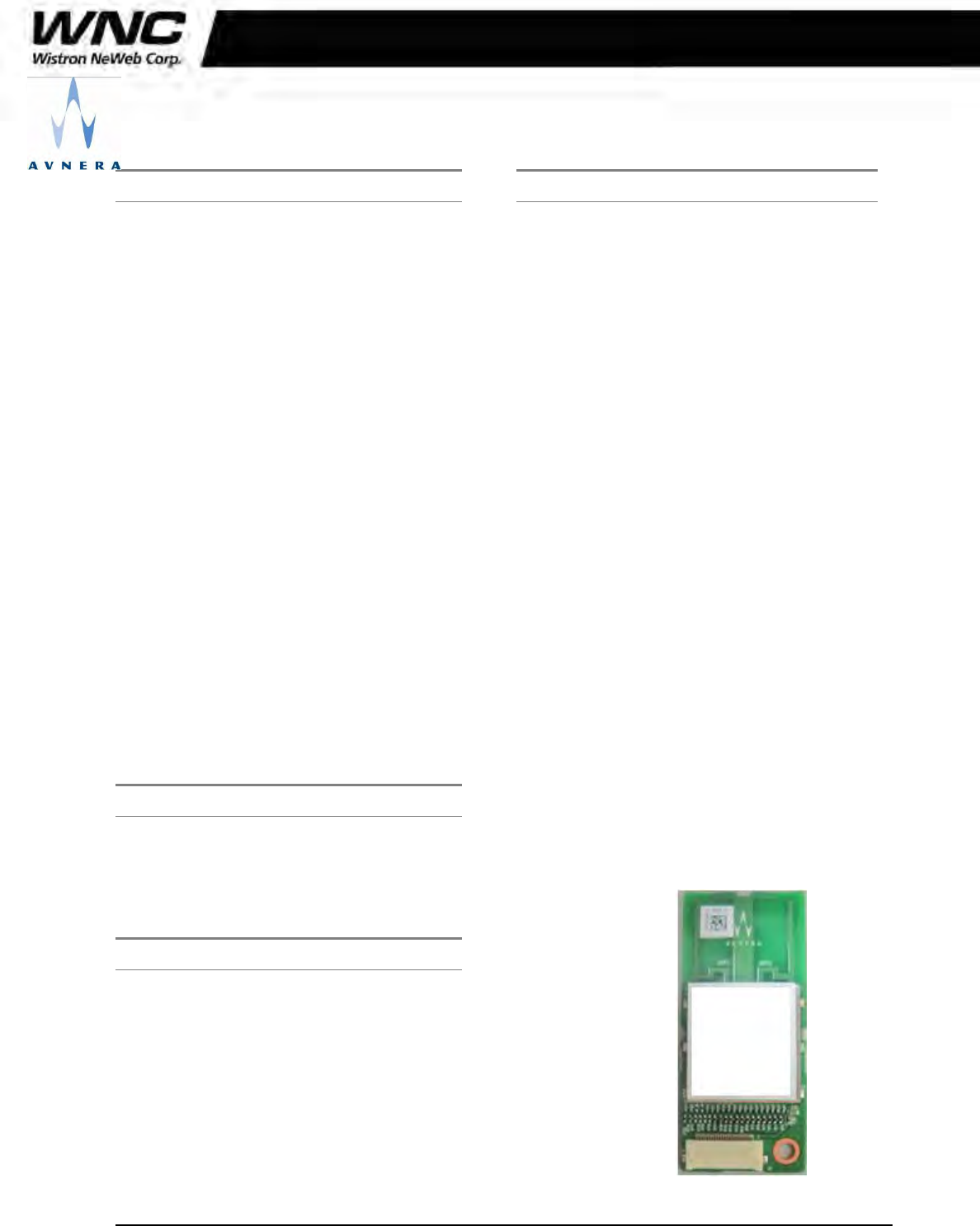
The module measures just 26 x 60 x 3.5 mm
and is provided with a 24 pin FPC connector
or pin header for connection to the system
board.
The module is certified to FCC and CE
standards.
Applications
Wireless Subwoofers
Stereo Wireless Rear Speakers
Soundbar / Audio Video Receiver / BluRay
Mono/Stereo Audio Channel Transmission
Ordering Options
SWA16-TX: Transmit module with digital audio
input
SWA16- RX: Receive module with digital
audio output
Features
Audio Interfaces
I2S Digital Input / Output interface with
>94dB end-to-end digital audio path
Wireless Range
> 15m Non Line Of Sight (NLOS) range
> 50m Line Of Sight (LOS) range
Frequency range: 2.4 GHz ISM band,
continuous dynamic frequency selection
Forward error correction coding, error
detection, and audio-specific error
concealment
Dual printed PCB diversity antennas for
multipath and fading mitigation
Auto-search/synch and dynamic channel
selection
Low and fixed latency
24 pin FPC or pin header connector
Sample rate converter: Support for 32 -
96kHz input sample rates
Over-the-air firmware update capability
Customizable firmware for simple, low-cost,
sub-woofer amplifier implementations
General purpose over-the-air (OTA) serial
interface:
11 kbps, bi-directional, full duplex
Support for amplifier control data, meta-
data, and remote control commands
SWA16-TX/RX
Module Datasheet
Mono/Stereo Wireless Audio System, based on the Avnera AV6100 IC
We use diff. label colors to
distinguish between TX and RX.

SWA16 Module Datasheet Rev 1.0
CONTENTS SUBJECT TO CHANGE WITHOUT NOTICE 2 CONFIDENTIAL
1 SWA16 Functional
The SWA16 module is available in 2 variations;
digital input transmitter module or digital output
receiver module. There is a separate I2S port for
digital audio input and output functions and either
of these can be configured to be a master or a
slave – only the input or output port can be active
at any time. In addition, MCLK can be generated
from the module, or input to the module as
required by the system application.
The hardware for the audio input (transmit) and
audio output (receive) versions of the module is
identical and only the firmware loaded on the
module determines its function.
The highly integrated nature of the AV6100
transceiver IC results in few external components
being required for the SWA16 module design. 2
Printed antennas are used to achieve increased
range, and to offer diversity, and the simple RF
path consists only of the antennas, associated
tuning components, the RF switch and a balun
connected to the AV6100 IC. A 16MHz crystal
generates the AV6100 system clock signal used
as the basis for all RF and digital audio signals. In
addition, a 2Mb flash memory stores the factory
based firmware, as well as firmware upgrade
images and configuration parameters. The module
firmware enables upgrades to be performed by the
I2C slave interface or over-the-air. The module
can be controlled from an external host device via
the I2C interface. The I2C master port allows the
module to control other system audio devices such
as a sub-woofer amplifier system without having to
add another MCU to the product design. Up to a
maximum of 17 GPIOs are supported with the
SWA16 module including I2C and I2S signals.
This large number of GPIOs can be leveraged to
implement low cost sub-woofer designs as
outlined below.
The SWA16 module offers a standard and low-
latency firmware with different over the air sample
rate. While the standard 22.2KSps over the air
sample rate optimizes audio quality and WiFi co-
existence performance; Lower audio latency can
be achieved by using the low-latency 44.4KSps
over the air sample rate.
1.1 Typical Sub-Woofer
Implementation
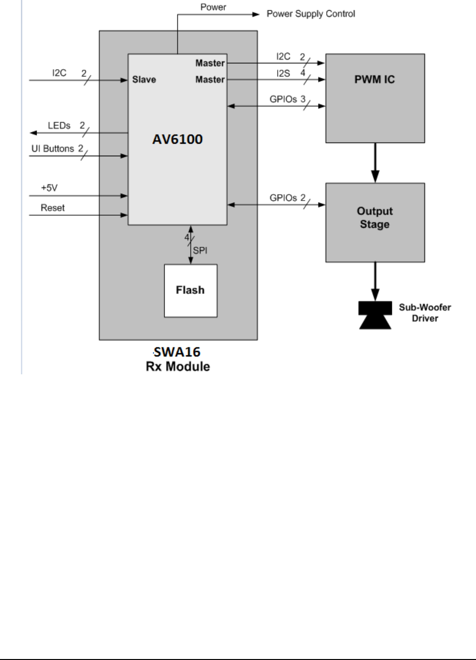
A simple low cost implementation of a sub-woofer
product design is shown in Figure 1. The sub
amplifier consists of a PWM chip plus an output
stage device, but no external MCU is required as
the SWA16 RX module performs the control
function using the I2C master communication port
in conjunction with multiple GPIOs. +5V power and
an optional reset signal are supplied to the SWA16
RX module and I2C slave communication can be
used to control the module if required. Several
GPIOs can be used to drive LEDs, or to connect to
UI buttons. Typically 2 LEDs may be used and 1
button for pairing purposes. Another button could
be used, for example, to implement a “bass
enhance” feature. Another GPIO can be used to
control the main power supply for the unit. The
SWA16 RX module will remain always powered up
but a GPIO control line is used to enable/disable
the higher voltage rail for the amplifier output
circuitry. If the wireless link is lost (when the sound
bar, or SWA16 TX module is powered down) the
SWA16 RX module can, after a timeout period,
power down the amplifier section to conserve
power and to help meet energy start requirements.
The I2C master port from the SWA16 RX module
can communicate, control, and initialize external
audio ICs such as the PWM chip in this example.
Other GPIOs can be used to detect fault
conditions (over temperature etc) and notify the
module. The audio is routed from the SWA16 RX
module to the amplifier circuit with the I2S output
port which can be configured as either a master or
a slave as required. MCLK can also be generated
from the SWA RX module as a ~12.288MHz clock
if required.
SWA16 Module Datasheet Rev 1.0
CONTENTS SUBJECT TO CHANGE WITHOUT NOTICE 3 CONFIDENTIAL
Figure 1: SWA16 RX Module Simple Sub-Woofer Implementation
SWA16 Module Datasheet Rev 1.0
CONTENTS SUBJECT TO CHANGE WITHOUT NOTICE 4 CONFIDENTIAL
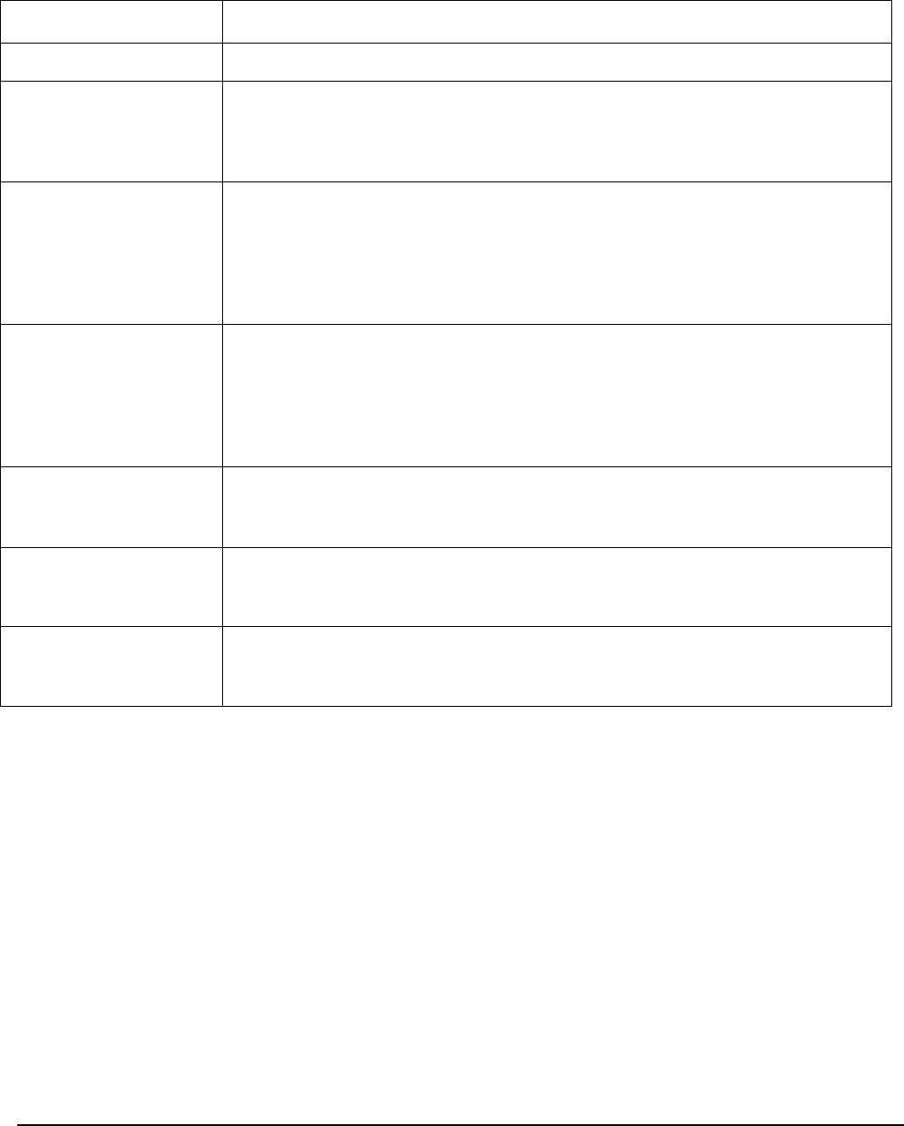
1.2 SWA16 Module Connections
Signal Type
Description
+5V Supply
Single +5V +/10% supply rail to the module
Reset
Active low reset input. This pin is driven from an open collector/drain device such
that it can pull to ground for the active reset state but, when released, must go to
a high impedance state. If this input is driven high the internal reset circuit on the
module will not operate correctly.
I2S In Port
The I2S input port can be configured as a master or slave. Consequently BCLK
and LRCK can be either inputs or outputs. In addition, MCLK can be generated
by the module on pin 16, or used as an input. Typically, as the AV6100 IC
contains a sample rate converter, MCLK is not required to be supplied to the
module when it is an I2S slave. CMOS 3.3 logic levels are used for all I2S
signals.
I2S Out Port
The I2S output port can be configured as a master or slave. Consequently BCLK
and LRCK can be either inputs or outputs. In addition, MCLK can be generated
by the module on pin 16, or used as an input. Typically, as the AV6100 IC
contains a sample rate converter, MCLK is not required to be supplied to the
module when it is an I2S slave. CMOS 3.3 logic levels are used for all I2S
signals.
I2C Slave Port
The I2C slave port is used for external host communication and during module
test. It is assumed that external pull up resistors are connected at the I2C master
communicating with the module.
I2C Master Port
The I2C master port is used to communicate with external audio devices such as
a sub-woofer amplifier. The SDA and SCL signal lines have pull ups internal to
the module.
GPIOs
3.3V CMOS logic level GPIOs available to connect to other devices, or to use as
UI supporting GPIOs for LED and button support. All supported GPIOs can be
configured as inputs or outputs.
SWA16 Module Datasheet Rev 1.0
CONTENTS SUBJECT TO CHANGE WITHOUT NOTICE 5 CONFIDENTIAL
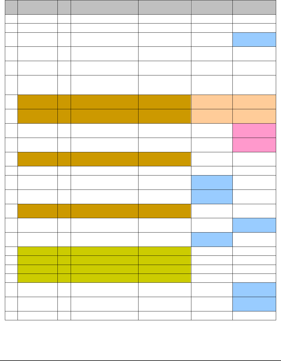
2 SWA16 Connector Information
No
Pin Name
I/O
AV6100
Pin Description
SWA16 TX
Module
SWA16 RX
Module
1
VDD
-
+5V +/- 10%
2
VDD
-
+5V +/- 10%
3
GPIO
I/O
GPIO13 pin 28
Function defined by
firmware application.
GPIO
ADOUT0 RX =
output
4
GPIO
I/O
GPIO18 pin 43
Function defined by
firmware application.
GPIO
GPIO
5
GPIO
I/O
GPIO19 pin 37
Function defined by
firmware application.
GPIO
GPIO
6
Reset
I
Pin 24
Driven from open
drain external source.
Can be left open.
Reset
Reset
7
I2C_SCL_S /
S_MISO
I/O
GPIO5 pin 44
I2C slave or SPI slave
port
I2C_SCL_S
LED RED,
firmware upgrade
8
I2C_SDA_S /
S_MOSI
I/O
GPIO4 pin 45
I2C slave or SPI slave
port
I2C_SDA_S
LED BLUE,
firmware upgrade
9
I2C_SCL_M
O
GPIO22 pin 41
I2C master port or
GPIO
GPIO
I2C_SCL_M
10
I2C_SDA_M
I/O
GPIO21 pin 42
I2C master port or
GPIO
GPIO
I2C_SDA_M
11
S_SCLK
I
GPIO3 pin 46
SPI slave port or
GPIO
GPIO
GPIO
12
GND
-
Ground
GND
GND
13
BCK1
I/O
GPIO15 pin 26
I2S port
BCLK1, TX
module = input
POWER
14
WCLK1
I/O
GPIO16 pin 25
I2S port
LRCK1, TX
module
GPIO
15
S_SSB
I
GPIO2 pin 47
SPI slave port or
GPIO
GPIO
GPIO
16
MCLK
I/O
GPIO10 pin 31
I2S port or GPIO
GPIO/MCLK
RX = 12.288MHz
output
17
ADIN1
I/O
GPIO14 pin 27
I2S port
ADIN1 TX =
input
GPIO
18
M_SSB/GPIO17
GPIO6 pin 36/GPIO17 pin 48
SPI master port
GPIO
GPIO
19
N.C
GPIO7pin 35/GPIO1 pin 1
SPI master port
NC
NC
20
N.C
GPIO8 pin 34
SPI master port
NC
NC
21
N.C
GPIO9 pin 33
SPI master port
NC
NC
22
GPIO
I/O
GPIO11 pin 30
Function defined by
firmware application.
LED1
BCLK0
23
GPIO
I/O
GPIO12 pin 29
Function defined by
firmware application.
LED2
WCLK0
24
GND
-
Ground
Table 1: SWA16 Connector Information
SWA16 Module Datasheet Rev 1.0
CONTENTS SUBJECT TO CHANGE WITHOUT NOTICE 6 CONFIDENTIAL
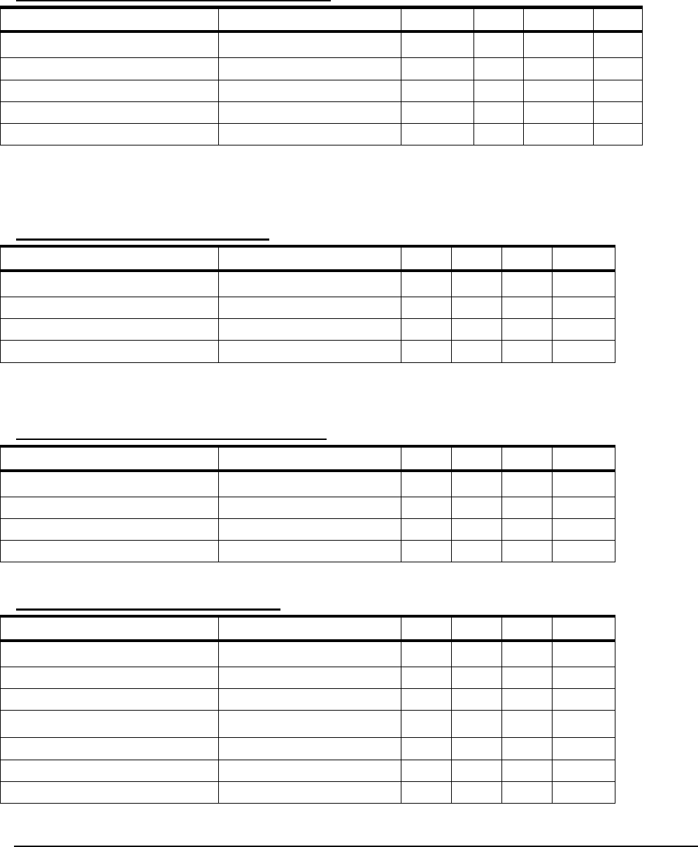
3 Electrical Specifications
3.1 Absolute Maximum Ratings
Absolute Maximum Ratings (AMR) are stress ratings only. AMR corresponds to the maximum value that can be applied without leading
to instantaneous or very short-term unrecoverable hard failure (destructive breakdown). Stresses beyond those listed under AMR may
cause permanent damage to the device.
Functional operation of the device at these or any other conditions beyond those indicated under “Recommended Operating Range” is
not implied. Exposure to absolute-maximum-rated conditions for extended periods may adversely affect device reliability.
Device functional operating limits and guaranteed performance specifications are given under Electrical Characteristics at the test
conditions specified.
CONDITION
MIN
MAX
+5V Supply Voltage Input
-0.3V
6.0V
Input Voltage Range – Digital
Inputs
-0.3V
3.6V
Operating Temperature
-10ºC
+70ºC
Storage Temperature
-20ºC
+80ºC
Static Discharge Voltage1
-6kV
+6kV
Notes:
Note 1: ±6kV @ bottom test pads, 150pF/330ohms discharge per IEC/EN61000-4-2
3.2 Recommended Operating Range
PARAMETER
MIN
TYP
MAX
UNIT
+5V Supply pin voltage
4.5
5.0
5.5
V
Ambient Temperature (TA)
0
60
ºC
SWA16 Module Datasheet Rev 1.0
CONTENTS SUBJECT TO CHANGE WITHOUT NOTICE 7 CONFIDENTIAL
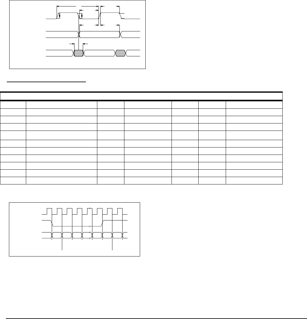
3.3 Electrical Characteristics
Test Conditions: TA=+25ºC, Vsupply=+5.0V
Table 2; SWA16 RF Transceiver Characteristics
PARAMETER
CONDITIONS
MIN
TYP
MAX
UNIT
RF Frequency Range
2405.35
2477.35
MHz
TX Output Power1
1.5
dBm
RX Sensitivity2
-91
-88
-85
dBm
Range (NLOS)
15
m
Range (LOS)
50
m
Note 1: Measured with the SWA16 Printed antenna disabled and test RF connector added.
Note 2: Measured with the SWA16 Printed antenna disabled and test RF connector added. Sensitivity is defined as the
onset of 0.2% BLER Clock Error Rate.
Table 3; SWA16 Audio Characteristics
PARAMETER
CONDITIONS
MIN
TYP
MAX
UNIT
Frequency Response1
20
10K
Hz
Gain Flatness2
0dB Input / Output Gain
±0.2
dB
SNR
I2S Input / Output
94
dB
THD+N
94
dB
Note 1: 16 bit audio, 22.2KSps over-the-air sample rate firmware build
Note 2: 16 bit audio, 22.2KSps over-the-air sample rate firmware build – 10KHz frequency response
Table 4; SWA16 Audio Latency Characteristics
PARAMETER
CONDITIONS
MIN
TYP
MAX
UNIT
22.2KSps OTA Sample Latency
Standard Firmware
17
ms
44.4KSps OTA Sample Latency
Standard Firmware
14
ms
22.2KSps OTA Sample Latency
Low Latency Firmware
13.5
ms
44.4KSps OTA Sample Latency
Low Latency Firmware
8.5
ms
Table 5; SWA16 Current Characteristics
PARAMETER
CONDITIONS
MIN
TYP
MAX
UNIT
TX Module Configuration
Linked1
35
mA
TX Module Configuration
Searching2
22
mA
TX Module Configuration
FCC TX3
63
mA
RX Module Configuration
Linked4
35
mA
RX Module Configuration
Searching5
63
mA
RX Module Configuration
Standby6
16
mA
RX Module Configuration
FCC TX7
71
mA
Note 1: Specification represents an average current with the I2S clocks running. Peak current is ~ 2x the average.
SWA16 Module Datasheet Rev 1.0
CONTENTS SUBJECT TO CHANGE WITHOUT NOTICE 8 CONFIDENTIAL
Note 2: Searching is the average current where the TX module is not linked but is attempting to find a RX module to link
with. Peak current is ~70mA.
Note 3: Continuous transmit mode for testing purposes. Peak current ~80mA.
Note 4: Specification represents an average current with the I2S clocks running. Peak current is ~ 2x the average.
Note 5: Searching is where the RX module is not linked but is attempting to find a TX module to link with. Peak current is ~
80mA.
Note 6:. After the RX module has not been linked for > 30 seconds it will go to a duty cycling standby state reflected by this
specification. Peak current is ~ 80mA.
Note 7: Continuous transmit mode for testing purposes. Peak current ~80mA.
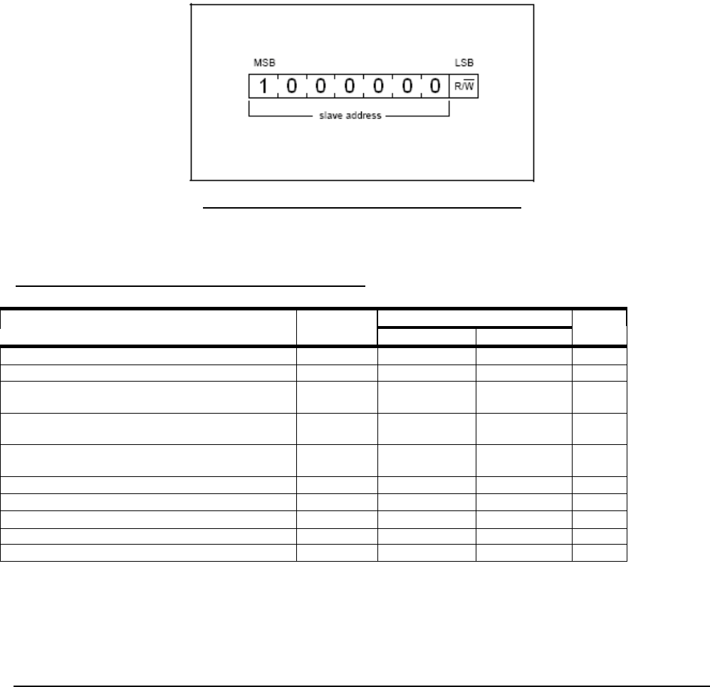
3.4 I2S Communication Interface Timing
I2S bit clock
TTHi<0.4T
TLo<0.4T VH=2.4V
VL=0.4V
I2S data input
I2S word clock input
TSu>25n THd>25n
I2S data output
I2S word clock output
-25n < Tod < 25n
TR<50n TF<50n
Table 6; SWA16 I2S Timing
MIN
TYP
MAX
UNIT
NOTES
VL
low voltage level
-0.3V
0.0V
0.4V
V
VH
high voltage level
2.4V
3.3V
3.6V
V
T
clock period
325.5n
s
1/3.072MHz
TLo
clock low period
0.4T
0.6T
THi
clock high period
0.4T
0.6T
TR
rise time
50n
s
Note 1
TF
fall time
50n
s
Note 1
TSu
setup time
25n
s
THd
hold time
25n
s
TOd
output delay
-25n
25n
s
bit clocks/word clock
64
I2S protocol is “I2S Justified” as shown below.
MSB LSB MSB
WORD n-1
RIGHT CHANNEL
WORD n
LEFT CHANNEL
WORD n+1
RIGHT CHANNEL
I2S bit clock
I2S data
I2S word clock
Note 1: The timing specified for the rise and fall times represents the edge rates on the module itself. The rise
and fall times of the I2S signals are determined by ESD/EMI mitigation components on the modules, as well
as external loading, and will be higher than the specified numbers
SWA16 Module Datasheet Rev 1.0
CONTENTS SUBJECT TO CHANGE WITHOUT NOTICE 9 CONFIDENTIAL
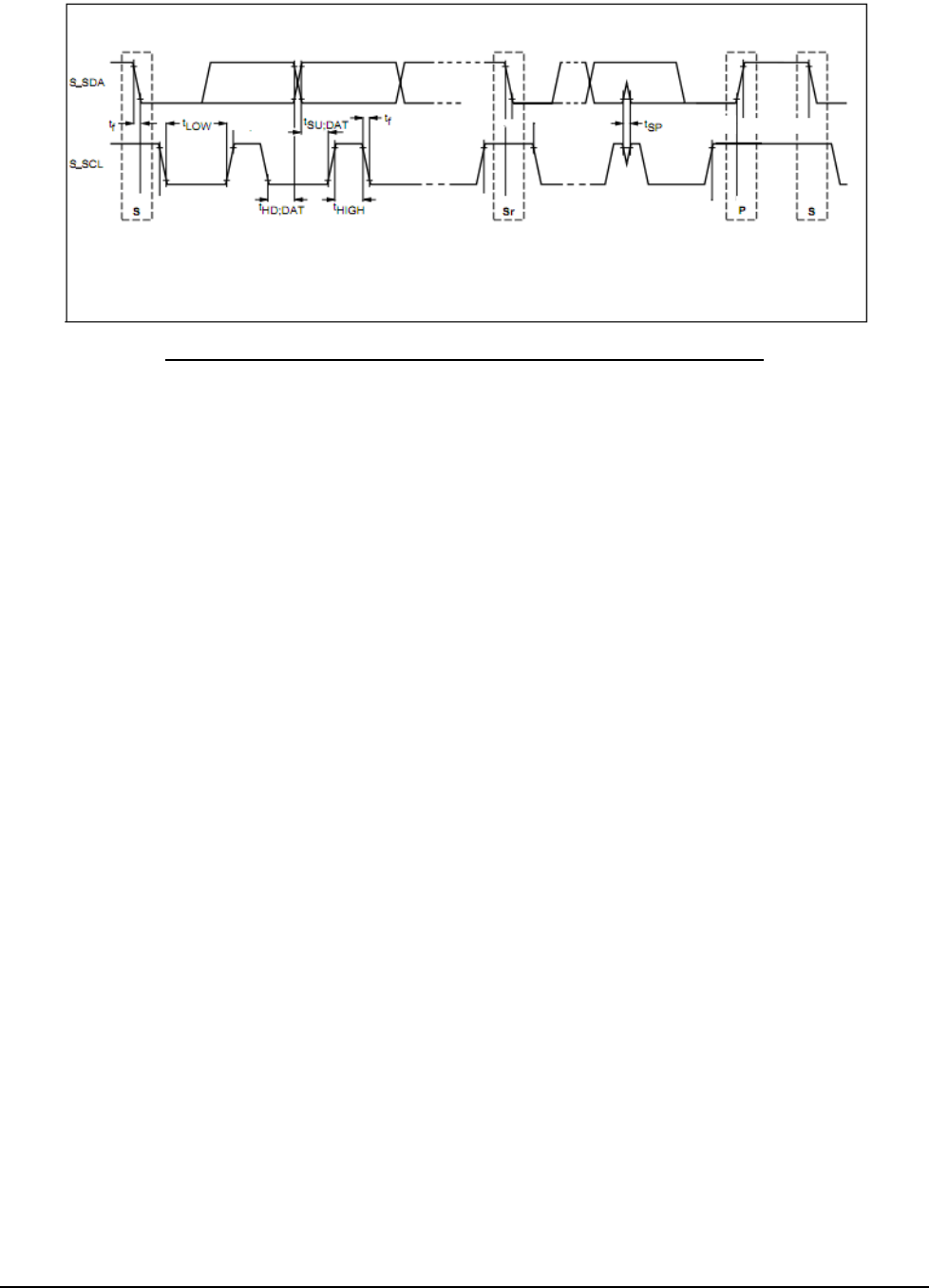
3.5 I2C Master/Slave Communication Interface Timing (S_SCL, S_SDA)
The SWA16 has both I2C slave and master interfaces available with their respective pins S_SCL and S_SDA.
The interfaces operate in I2C fast-mode and can receive and transmit at up to 400 kbit/s.
Bytes are 8 bits long and are transferred with the most significant bit (MSB) first. Each byte has to be followed
by an acknowledge bit. The SWA16 will apply clock-stopping (by holding the clock line S_SCL LOW to force
the master into a wait state) if necessary due to internal high-priority tasks.
The slave/master interface can be used both for writing (e.g. sending commands) or reading (e.g. requesting
status).
The SWA16 slave interface responds to the 7-bit slave address 1000000 (0x40) as shown in Figure 2 below.
Figure 2: First Byte After the START Procedure
ELECTRICAL SPECIFICATIONS AND TIMING
Table 6; Characteristics of the S_SDA and S_SCL I/Os
PARAMETER
SYMBOL
FAST-MODE
UNIT
MIN.
MAX.
LOW level input voltage
VIL
0.3
0.8
V
HIGH level input voltage
VIH
2.0
3.6
V
LOW level output voltage (open drain or
open collector) at 1 mA sink current:
VOL
0
0.4
V
Output fall time from VIHmin to VILmax with
a bus capacitance from 10 pF to 400 pF
tof
0
250
ns
Pulse width of spikes which must be
suppressed by the input filter
tSP
0
50
ns
S_SCL clock frequency
fSCL
0
400
kHz
LOW period of the S_SCL clock
tLOW
1.3
–
s
HIGH period of the S_SCL clock
tHIGH
0.6
–
s
Data hold time
tHD;DAT
100
–
ns
Data set-up time
tSU;DAT
100
–
ns
SWA16 Module Datasheet Rev 1.0
CONTENTS SUBJECT TO CHANGE WITHOUT NOTICE 10 CONFIDENTIAL
Figure 3: Definition of Timing for F/S-Mode Devices on the I2C-Bus

SWA16 Module Datasheet Rev 1.0
CONTENTS SUBJECT TO CHANGE WITHOUT NOTICE 11 CONFIDENTIAL
Ordering Information
Table 7: SWA16 Module Ordering Information
Module Part
Number
Option
Code
Description
SWA16
-TX
Digital Input , FPC Connector, integrated printed
antennas
SWA16
-RX
Digital Output, FPC Connector, integrated printed
antennas

SWA16 Module Datasheet Rev 1.0
CONTENTS SUBJECT TO CHANGE WITHOUT NOTICE 12 CONFIDENTIAL
FCC Statement:
Federal Communication Commission Interference Statement
This equipment has been tested and found to comply with the limits for a Class B digital device, pursuant to
Part 15 of the FCC Rules. These limits are designed to provide reasonable protection against harmful
interference in a residential installation. This equipment generates, uses and can radiate radio frequency
energy and, if not installed and used in accordance with the instructions, may cause harmful interference to
radio communications. However, there is no guarantee that interference will not occur in a particular
installation. If this equipment does cause harmful interference to radio or television reception, which can be
determined by turning the equipment off and on, the user is encouraged to try to correct the interference by
one of the following measures:
● Reorient or relocate the receiving antenna.
● Increase the separation between the equipment and receiver.
● Connect the equipment into an outlet on a circuit different from that to which the receiver is connected.
● Consult the dealer or an experienced radio/TV technician for help.
This device complies with Part 15 of the FCC Rules. Operation is subject to the following two conditions: (1)
This device may not cause harmful interference, and (2) this device must accept any interference received,
including interference that may cause undesired operation.
This device and its antenna(s) must not be co-located with any other transmitters except in
accordance with FCC multi-transmitter product procedures.
Refering to the multi-transmitter policy, multiple-transmitter(s) and module(s) can be operated
simultaneously without C2P.
IMPORTANT NOTE:
This module is intended for OEM integrator. The OEM integrator is responsible for the compliance
to all the rules that apply to the product into which this certified RF module is integrated.
Additional testing and certification may be necessary when multiple modules are used.
20cm minimum distance has to be able to be maintained between the antenna and the users for the host this
module is integrated into. Under such configuration, the FCC radiation exposure limits set forth for an
population/uncontrolled environment can be satisfied.
Any changes or modifications not expressly approved by the manufacturer could void the user's authority to
operate this equipment.

SWA16 Module Datasheet Rev 1.0
CONTENTS SUBJECT TO CHANGE WITHOUT NOTICE 13 CONFIDENTIAL
USERS MANUAL OF THE END PRODUCT:
In the users manual of the end product, the end user has to be informed to keep at least 20cm separation with
the antenna while this end product is installed and operated. The end user has to be informed that the FCC
radio-frequency exposure guidelines for an uncontrolled environment can be satisfied. The end user has to
also be informed that any changes or modifications not expressly approved by the manufacturer could void
the user's authority to operate this equipment. If the size of the end product is smaller than 8x10cm, then
additional FCC part 15.19 statement is required to be available in the users manual: This device complies
with Part 15 of FCC rules. Operation is subject to the following two conditions: (1) this device may not cause
harmful interference and (2) this device must accept any interference received, including interference that
may cause undesired operation.
LABEL OF THE END PRODUCT:
The final end product must be labeled in a visible area with the following " Contains TX FCC ID: NKR-SWA16
". If the size of the end product is larger than 8x10cm, then the following FCC part 15.19 statement has to also
be available on the label: This device complies with Part 15 of FCC rules. Operation is subject to the
following two conditions: (1) this device may not cause harmful interference and (2) this device must accept
any interference received, including interference that may cause undesired operation.
SWA16 Module Datasheet Rev 1.0
CONTENTS SUBJECT TO CHANGE WITHOUT NOTICE 14 CONFIDENTIAL
IC Statement:
This device complies with Industry Canada license-exempt RSS standard(s). Operation is subject to the
following two conditions: (1) this device may not cause interference, and (2) this device must accept any
interference, including interference that may cause undesired operation of the device.
Le présent appareil est conforme aux CNR d'Industrie Canada applicables aux appareils radio
exempts de licence. L'exploitation est autorisée aux deux conditions suivantes : (1) l'appareil ne doit
pas produire de brouillage, et (2) l'utilisateur de l'appareil doit accepter tout brouillage
radioélectrique subi, même si le brouillage est susceptible d'en compromettre le fonctionnement.
This device and its antenna(s) must not be co-located with any other transmitters except in
accordance with IC multi-transmitter product procedures.
Refering to the multi-transmitter policy, multiple-transmitter(s) and module(s) can be operated
simultaneously without reassessment permissive change.
Cet appareil et son antenne (s) ne doit pas être co-localisés ou fonctionnement en association avec
une autre antenne ou transmetteur.
IMPORTANT NOTE:
IC Radiation Exposure Statement:
This equipment complies with IC RSS-102 radiation exposure limits set forth for an uncontrolled environment.
This equipment should be installed and operated with minimum distance 20cm between the radiator & your
body.
Cet équipement est conforme aux limites d'exposition aux rayonnements IC établies pour un
environnement non contrôlé. Cet équipement doit être installé et utilisé avec un minimum de 20 cm
de distance entre la source de rayonnement et votre corps.
This module is intended for OEM integrator. The OEM integrator is still responsible for the IC compliance
requirement of the end product, which integrates this module.
USERS MANUAL OF THE END PRODUCT:
In the users manual of the end product, the end user has to be informed to keep at least 20cm separation with
the antenna while this end product is installed and operated. The end user has to be informed that the IC
radio-frequency exposure guidelines for an uncontrolled environment can be satisfied. The end user has to
also be informed that any changes or modifications not expressly approved by the manufacturer could void
the user's authority to operate this equipment. Operation is subject to the following two conditions: (1) this
device may not cause harmful interference and (2) this device must accept any interference received,
including interference that may cause undesired operation.
LABEL OF THE END PRODUCT:
The final end product must be labeled in a visible area with the following " Contains TX IC : 4441A-SWA16 ".