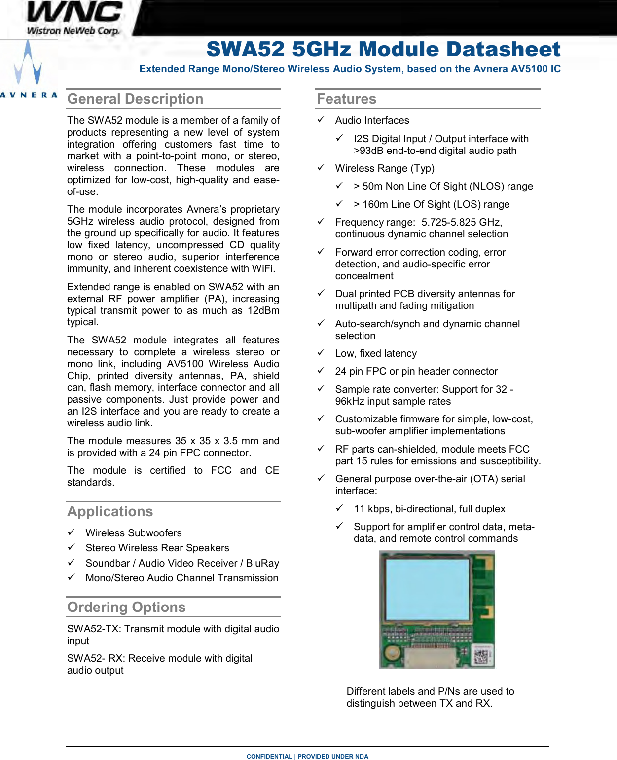
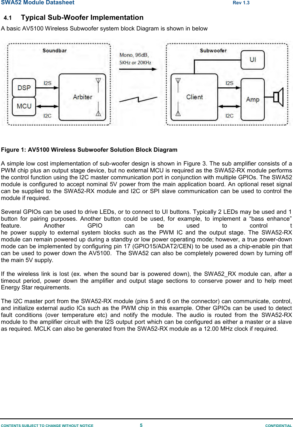
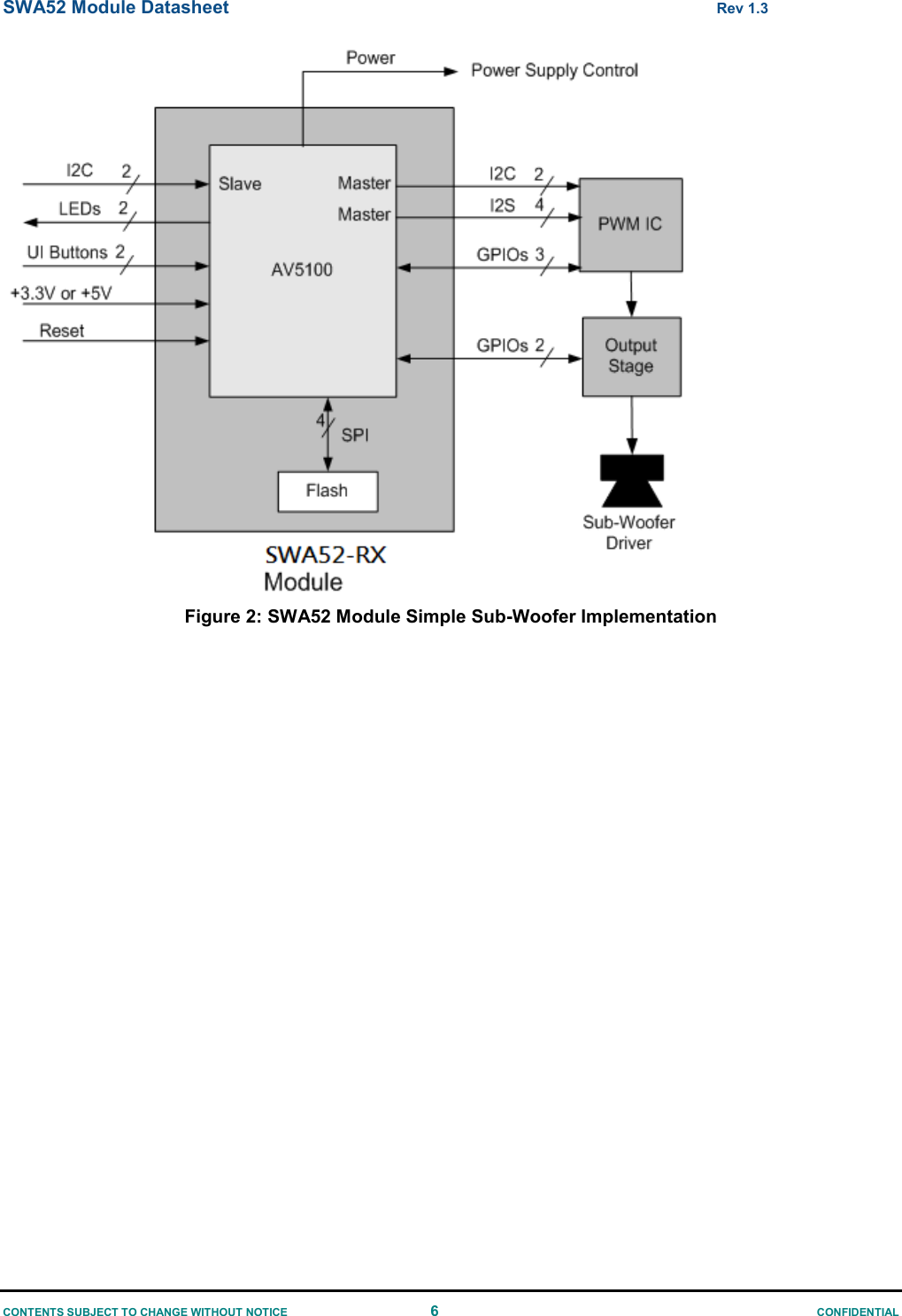
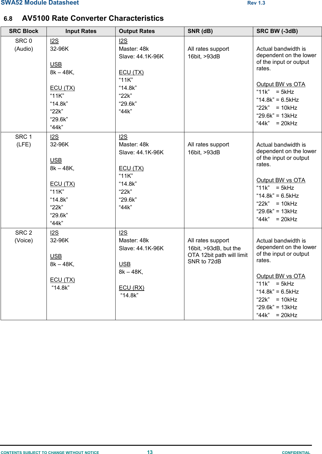
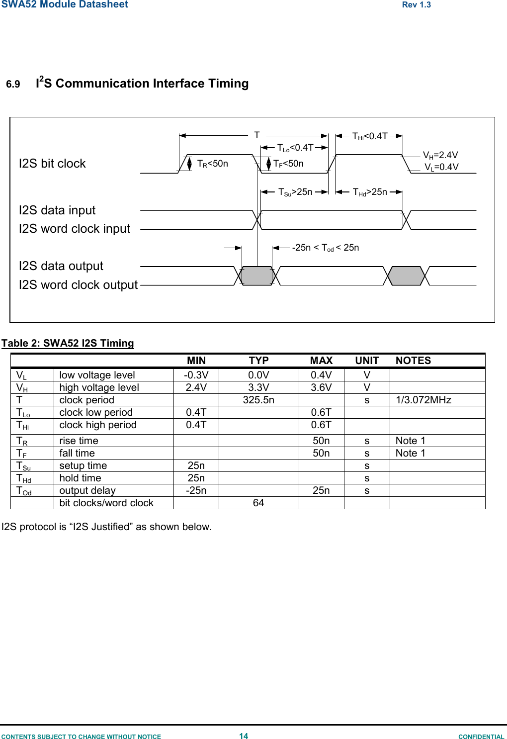
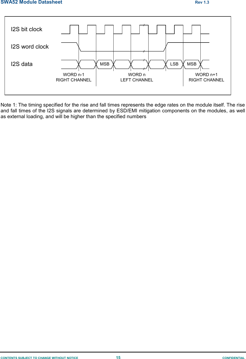
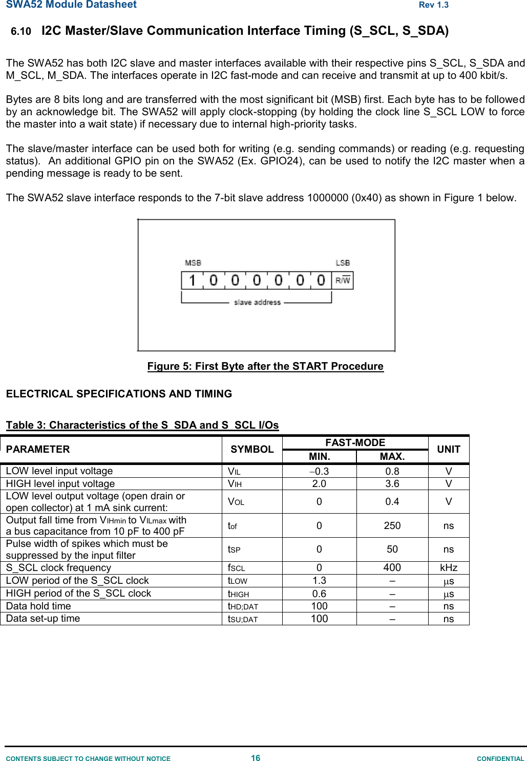
Wistron NeWeb SWA52 Wireless Audio Module User Manual

Wistron NeWeb Corporation Wireless Audio Module Users Manual

Contents

Users Manual

CONFIDENTIAL | PROVIDED UNDER NDA    General Description The SWA52 module is a member of a family of products  representing  a  new  level  of  system integration  offering  customers  fast  time  to market  with  a  point-to-point  mono,  or  stereo, wireless  connection.  These  modules  are optimized  for  low-cost,  high-quality  and  ease-of-use.  The module incorporates  Avnera’s  proprietary 5GHz  wireless  audio  protocol,  designed  from the ground up specifically for audio. It features low  fixed  latency,  uncompressed  CD  quality mono  or  stereo  audio,  superior  interference immunity, and inherent coexistence with WiFi. Extended range is enabled on SWA52 with an external  RF  power  amplifier  (PA),  increasing typical  transmit  power  to  as  much  as  12dBm typical. The  SWA52  module  integrates  all  features necessary  to  complete  a  wireless  stereo  or mono  link,  including  AV5100  Wireless  Audio Chip,  printed  diversity  antennas,  PA,  shield can, flash memory, interface connector and all passive  components.  Just  provide  power  and an I2S interface and you are ready to create a wireless audio link. The module measures 35 x 35 x  3.5 mm and is provided with a 24 pin FPC connector.  The  module  is  certified  to  FCC  and  CE standards. Applications   Wireless Subwoofers   Stereo Wireless Rear Speakers   Soundbar / Audio Video Receiver / BluRay  Mono/Stereo Audio Channel Transmission   Ordering Options SWA52-TX: Transmit module with digital audio input SWA52- RX: Receive module with digital audio output  Features   Audio Interfaces   I2S Digital Input / Output interface with >93dB end-to-end digital audio path   Wireless Range (Typ)  > 50m Non Line Of Sight (NLOS) range  > 160m Line Of Sight (LOS) range   Frequency range:  5.725-5.825 GHz, continuous dynamic channel selection   Forward error correction coding, error detection, and audio-specific error concealment   Dual printed PCB diversity antennas for multipath and fading mitigation   Auto-search/synch and dynamic channel selection   Low, fixed latency    24 pin FPC or pin header connector   Sample rate converter: Support for 32 - 96kHz input sample rates   Customizable firmware for simple, low-cost, sub-woofer amplifier implementations   RF parts can-shielded, module meets FCC part 15 rules for emissions and susceptibility.   General purpose over-the-air (OTA) serial interface:    11 kbps, bi-directional, full duplex   Support for amplifier control data, meta-data, and remote control commands      SWA52 5GHz Module Datasheet Extended Range Mono/Stereo Wireless Audio System, based on the Avnera AV5100 IC  Different labels and P/Ns are used to distinguish between TX and RX.
SWA52 Module Datasheet  Rev 1.3 CONTENTS SUBJECT TO CHANGE WITHOUT NOTICE  2  CONFIDENTIAL 1  Table of Contents General Description ............................................................................................................ 1 Applications ........................................................................................................................ 1 Ordering Options ................................................................................................................ 1 Features ............................................................................................................................... 1 1 Table of Contents ......................................................................................................... 2 2 Lists of Figures and Tables ......................................................................................... 3 3 Revision History ........................................................................................................... 3 4 SWA52 Functional Description ................................................................................... 4 4.1 Typical Sub-Woofer Implementation ............................................................................................... 5 4.2 SWA52 Module Connections and Interfaces .................................................................................. 7 5 SWA52 Connector Information ................................................................................... 8 6 Electrical, Audio and Timing Specifications ............................................................ 10 6.1 Absolute Maximum Ratings ........................................................................................................... 10 6.2 Recommended Operating Range ................................................................................................... 10 6.3 Electrical Characteristics – DC Characteristics ........................................................................... 10 6.4 Electrical Characteristics – RF PLL Characteristics.................................................................... 11 6.5 Electrical Characteristics – RF RX Characteristics ..................................................................... 11 6.6 Electrical Characteristics – RF TX Characteristics ...................................................................... 12 6.7 Electrical Characteristics – Audio C/CS ....................................................................................... 12 6.8 AV5100 Rate Converter Characteristics ....................................................................................... 13 6.9 I2S Communication Interface Timing ............................................................................................. 14 6.10 I2C Master/Slave Communication Interface Timing (S_SCL, S_SDA) ..................................... 166 7 Ordering Information.................................................................................................. 17
SWA52 Module Datasheet  Rev 1.3 CONTENTS SUBJECT TO CHANGE WITHOUT NOTICE  3  CONFIDENTIAL 2  Lists of Figures and Tables Table 1: SWA52 Connector Information ............................................................................................................. 8 Table 2: SWA52 I2S Timing .............................................................................................................................. 14 Table 3: Characteristics of the S_SDA and S_SCL I/Os .................................................................................. 16 Table 4: SWA52 Module Ordering Information ................................................................................................. 17  Figure 1: AV5100 Wireless Subwoofer Solution Block Diagram .................................................................. 5   3  Revision History Revision Description of Changes Date 1.0 Initial Draft 11/26/2015 1.3 Final version 12/24/2015
SWA52 Module Datasheet  Rev 1.3 CONTENTS SUBJECT TO CHANGE WITHOUT NOTICE  4  CONFIDENTIAL 4  SWA52 Functional Description   The  SWA52  module  is  available  in  2  variations;  digital  input  transmitter  module  or  digital  output  receiver module.   There are three available I2S digital audio data inputs/outputs, each of these can be configured to operate as either a master or a slave - depending on the application, the I2S ports can operate simultaneously as either inputs or outputs. When configured as slaves, the I2S inputs/outputs can be independently clocked by up to two external masters. In addition, MCLK can be output from the module to provide a reference clock source to an  external  ADC  or  DAC.  MCLK  can  also  be  input  to  the  module  to  provide  a  reference  clock  from  an external source.  The hardware for the audio input (transmit) and audio output (receive) versions of the module is identical and only the firmware loaded onto the module determines its function.   The highly integrated nature of the AV5100 transceiver IC results in few external components being required for the SWA52 module design. 2 printed PCB antennas are used to achieve increased range, and to achieve antenna  spatial  diversity.  The  extended-range  RF  path  consists  of  the  antennas,  associated  tuning components, shield can, the RF switch, RF power amplifer (PA) and two baluns, one connected to each of the RF input/output ports on the AV5100 IC.   A 16MHz crystal oscillator generates the AV5100 fundamental system clock used as the basis for all RF and digital audio clocks.   A 2Mb flash memory chip is used to store the module’s application firmware. The AV5100 is able to boot from internal  ROM upon  first  power up,  which  enables programming  the  flash  chip with  the application  firmware  through USB. In addition,  Over-the-air Firmware upgrade capability can  be enabled  through the  application firmware. The module can be controlled from an external host device via the I2C Slave or the SPI Slave data interfaces.  The  I2C  master  port  allows  the  module  to  control  other  system  audio  devices  such  as  a  sub-woofer amplifier system without having to add another MCU to the product design. Up to 9 additional GPIOs are available on the SWA52 module (not including I2C and I2S signals) for implementing different UI features on  the  target  application.  The  resources  mentioned  above  can  be  leveraged  to  implement  low  cost  sub-woofer designs as outlined below.
SWA52 Module Datasheet  Rev 1.3 CONTENTS SUBJECT TO CHANGE WITHOUT NOTICE  5  CONFIDENTIAL 4.1 Typical Sub-Woofer Implementation A basic AV5100 Wireless Subwoofer system block Diagram is shown in below     Figure 1: AV5100 Wireless Subwoofer Solution Block Diagram   A simple low cost implementation of sub-woofer design is shown in Figure 3. The sub amplifier consists of a PWM chip plus an output stage device, but no external MCU is required as the SWA52-RX module performs the control function using the I2C master communication port in conjunction with multiple GPIOs. The SWA52 module is configured to accept nominal 5V power from the main application board. An optional reset signal can be  supplied to the SWA52-RX  module and I2C or SPI slave communication can be used to control the module if required.   Several GPIOs can be used to drive LEDs, or to connect to UI buttons. Typically 2 LEDs may be used and 1 button  for  pairing  purposes.  Another  button  could  be  used,  for  example,  to  implement  a  “bass  enhance” feature.  Another  GPIO  can  be  used  to  control  the  power  supply  to  external  system  blocks  such  as  the  PWM  IC  and  the  output  stage.  The  SWA52-RX module can remain powered up during a standby or low power operating mode; however, a true power-down mode can be implemented by configuring pin 17 (GPIO15/ADAT2/CEN) to be used as a chip-enable pin that can be used to power down the AV5100.  The SWA52 can also be completely powered down by turning off the main 5V supply.   If  the  wireless  link  is  lost  (ex.  when  the  sound  bar  is  powered  down),  the  SWA52_RX module can,  after  a timeout  period,  power  down  the  amplifier  and  output  stage  sections  to  conserve  power  and  to  help  meet Energy Star requirements.  The I2C master port from the SWA52-RX module (pins 5 and 6 on the connector) can communicate, control, and initialize external audio ICs such as the PWM chip in this example. Other GPIOs can be used to detect fault  conditions  (over  temperature  etc)  and  notify  the  module.  The  audio  is  routed  from  the  SWA52-RX module to the amplifier circuit with the I2S output port which can be configured as either a master or a slave as required. MCLK can also be generated from the SWA52-RX module as a 12.00 MHz clock if required.
SWA52 Module Datasheet  Rev 1.3 CONTENTS SUBJECT TO CHANGE WITHOUT NOTICE  6  CONFIDENTIAL Figure 2: SWA52 Module Simple Sub-Woofer Implementation
SWA52 Module Datasheet  Rev 1.3 CONTENTS SUBJECT TO CHANGE WITHOUT NOTICE  7  CONFIDENTIAL 4.2  SWA52 Module Connections and Interfaces  Signal Type Description +5.0V Supply The SWA52 hardware is configured to accept a nominal +5.0V supply.   Reset Active low reset input. This pin is driven from an open collector/drain device such that it can be pulled to ground for the active reset state but, when released, must go to a high impedance state. This pin should not be actively driven high, as the AV5100 internal reset circuit will not operate correctly. I2S In Port The I2S input port can be configured as a master or slave. Consequently BCLK and LRCK can be either inputs or outputs. In addition, MCLK can be sourced by the module on pin 16.  Since the AV5100 IC contains a sample rate converter, MCLK  is  not  required  to  be  supplied  to  the  module  when  it  is  an  I2S  slave. CMOS 3.3V logic levels are used for all I2S signals. I2S Out Port The I2S output port can be configured as a master or slave. Consequently BCLK and LRCK can be either inputs or outputs. In addition, MCLK can be sourced by the module on pin 16.  Since the AV5100 IC contains a sample rate converter, MCLK  is  not  required  to  be  supplied  to  the  module  when  it  is  an  I2S  slave. CMOS 3.3V logic levels are used for all I2S signals. I2C Slave Port The I2C slave port can be used for external host communication and for module testing.  It  is  assumed  that  external  pull  up  resistors  are  connected  at  the  I2C master communicating with the module. I2C Master Port The I2C master port is used to communicate with external audio devices such as a sub-woofer amplifier. It is assumed that external pull up resistors are included on the application board. GPIOs 3.3V CMOS logic level GPIOs available to connect to other devices, or to use as UI supporting GPIOs for  LED  and  button support.  All supported GPIOs can  be configured as outputs or inputs with configurable pull-ups/pull-downs.
SWA52 Module Datasheet  Rev 1.3 CONTENTS SUBJECT TO CHANGE WITHOUT NOTICE  8  CONFIDENTIAL 5  SWA52 Connector Information Table 1: SWA52 Connector Information  No Pin Name Pin Type AV65100 Pin  SWA52-TX Pin Description SWA52-RX Pin Description 1 GPIO2/S_SSB Digital I/O 12 GPIO or SPI Slave Chip Select GPIO or SPI Slave Chip Select 2 GPIO3/S_SCLK Digital I/O 11  GPIO or SPI Slave Serial Clock GPIO or SPI Slave Serial Clock 3 GPIO4/S_SDA/S_MOSI Digital I/O 10 GPIO,  I2C Slave Serial Data or SPI Slave Data In GPIO,  I2C Slave Serial Data or SPI Slave Data In 4 GPIO5/S_SCL/S_MISO Digital I/O 9 GPIO,  I2C Slave Serial Clock or SPI Slave Data Out GPIO,  I2C Slave Serial Clock or SPI Slave Data Out 5 GPIO16/M_SDA Digital I/O 4  GPIO,  I2C Master Serial Data GPIO,  I2C Master Serial Data 6 GPIO17/M_SCL Digital I/O 3 GPIO,  I2C Master Serial Clock GPIO,  I2C Master Serial Clock 7 GPIO20/LINK_LED Digital I/O 56 GPIO,  or LINK_LED Output GPIO,  or LINK_LED Output 8 GPIO21/PAIR Digital I/O 55 GPIO,  or input from PAIR Button GPIO,  or input from PAIR Button 9 GPIO18/BCLK1 Digital I/O 2 GPIO or I2S Port 1 Bit Clock  GPIO or I2S Port 1 Bit Clock 10 GPIO19/WCLK1 Digital I/O 1 GPIO or I2S Port 1 Word Clock GPIO or I2S Port 1 Word Clock 11 GPIO10/MCLK Digital I/O 53 GPIO or Master Clock Out GPIO or Master Clock Out 12 GND GND Paddle (57) GND GND 13 GPIO11/BCLK0 Digital I/O 52 GPIO or I2S Port 0 Bit Clock GPIO or I2S Port 0 Bit Clock 14 GPIO12/WCLK0 Digital I/O 51 GPIO or I2S Port 0 Word Clock GPIO or I2S Port 0 Word Clock 15 GPIO13/ADAT0 Digital I/O 50 GPIO or I2S Port 0 Audio Data GPIO or I2S Port 0 Audio Data 16 GPIO14/ADAT1 Digital I/O 49 GPIO or I2S Port 1 Audio Data GPIO or I2S Port 1 Audio Data 17 GPIO15/ADAT2/CEN Digital I/O or Digital Input 48 or 38 GPIO,  I2S Port 2 Audio Data or chip enable (1) GPIO,  I2S Port 2 Audio Data or chip enable (1)
SWA52 Module Datasheet  Rev 1.3 CONTENTS SUBJECT TO CHANGE WITHOUT NOTICE  9  CONFIDENTIAL 18 GPIO22/D+ Digital I/O 47 or 43 GPIO or USB Data Plus (2) GPIO or USB Data Plus (2) 19 GPIO23/D- Digital I/O 46 or 42 GPIO or USB Data Minus (2) GPIO or USB Data Minus (2) 20 GPIO24 Digital I/O 41 GPIO (3) GPIO (3) 21 RESETN_EXT Digital Input 37 RESET signal active low (4) RESET signal active low (4) 22 GND GND Paddle (57) GND GND 23 VDD Supply Input 31, 45, 54 +5.0V input supply voltage  +5.0V input supply voltage  24 VDD Supply Input 31, 45, 54 +5.0V input supply voltage  +5.0V input supply voltage   Notes: (1)  Pin 17 is hardware configured as GPIO15/ADAT2 by default; utilizing this pin as a CEN requires a different  stuffing option. (2)  Utilizing pins 18 and 19 as USB D+ and D- requires the firmware to Tri-state GPIOs 22 and 23. (3)  Pin 20 (GPIO24) can be utilized to implement a “Data Waiting” interrupt signal for I2C and SPI Slave data communication. (4)  Pin 21 (RESET_EXT) can be pulled to GND with a switch or an open drain/collector type device to provide a hard reset signal to the AV5100.  This pin is pulled up to VDDIO (3.3V) internally in the AV5100 and should not be actively driven high
SWA52 Module Datasheet  Rev 1.3 CONTENTS SUBJECT TO CHANGE WITHOUT NOTICE  10  CONFIDENTIAL 6  Electrical, Audio and Timing Specifications  6.1 Absolute Maximum Ratings Absolute Maximum Ratings (AMR) are stress ratings only. AMR corresponds to the maximum value that can be applied without leading to instantaneous  or  very  short-term  unrecoverable  hard  failure  (destructive  breakdown).  Stresses  beyond  those  listed  under  AMR  may cause permanent damage to the device. Functional operation of the device at these or any other conditions beyond those indicated under “Recommended Operating Range” is not implied. Exposure to absolute-maximum-rated conditions for extended periods may adversely affect device reliability. Device  functional  operating  limits  and  guaranteed  performance  specifications  are  given  under  Electrical  Characteristics  at  the  test conditions specified.   CONDITION MIN MAX +5V Supply Voltage Input -0.3V 6.0V Input Voltage Range – Digital Inputs -0.3V 3.6V Input Voltage Range – Analog Inputs -0.3V 3.6V Operating Temperature -40ºC +60ºC  Storage Temperature -40ºC +70ºC Static Discharge Voltage1 2kV ---- Notes: ) HBM = ESD Hua Body Model; C = pF, R = kΩ  6.2 Recommended Operating Range PARAMETER MIN TYP MAX UNIT VDD, +5V Supply pin voltage 4.5 5.0 5.5 V Ambient Temperature (TA) 0  55 ºC  RESET pin hold time 10   msec Power Supply Rise Time (to 3.0V) 0  10 msec       6.3 Electrical Characteristics – DC Characteristics Operating Conditions: VDD = 4.5 to 5.5V, TA = 0°C to +55 °C, RF Fe = 55‐525MHz, measured relative to the RF balun sigle‐eded I/O. Typical specificatios at TA = 25°C, VDD = 5.0V 5V. PARAMETER CONDITIONS MIN TYP MAX UNIT Supply Current (IVDDA) Shutdown (chip disabled)  Standby (also USB suspend) RX mode (continuous RX) TX mode (continuous TX); Pout=+12dBm  TBD  TBD  89  330 1  2.5 uA  mA  mA  mA
SWA52 Module Datasheet  Rev 1.3 CONTENTS SUBJECT TO CHANGE WITHOUT NOTICE  11  CONFIDENTIAL CMOS I/O Logic Levels – 3.3V I/O Input Voltage Logic Low, VIL    0.6 V Input Voltage Logic High, VIH  VDDIO ‐0.6   V Output Voltage Logic Low, VOL    0.3 V Output Voltage Logic High, VOH  VDDIO ‐0.3   V  6.4 Electrical Characteristics – RF PLL Characteristics Operating Conditions: VDD =4.5 to 5.5V, TA = 0°C to +55 °C, RF Fe = 55‐525MHz, measured relative to the RF balun sigle‐eded I/O. Typical specifications at TA = 25°C, VDD = 5.0V PARAMETER CONDITIONS MIN TYP MAX UNIT RF Channel Frequency Range Band4(Upper band) 5725  5825 MHz RF Channel frequency resolution (raster)   1  MHz RF I/O Impedance ANT0,ANT1  50  ohm Crystal Oscillator Frequency External crystal  16  MHz Crystal Accuracy Requirement External XTAL, -20°C to +70 °C   +/-20 ppm         6.5 Electrical Characteristics – RF RX Characteristics Operating Conditions: VDD = 4.5 to 5.5V, TA = 0°C to +55 °C, RF Fe = 55‐525MHz, measured relative to the RF balun sigle‐eded I/O. Typical specificatios at TA = 25°C, VDD = 5.0V PARAMETER CONDITIONS MIN TYP MAX UNIT RF Channel Frequency Range Band4(Upper band) 5725  5825 MHz RF I/O Impedance ANT0,ANT1  50  ohm RX Sensitivity SSC (single sub-carrier) DSC (dual sub-carrier)  -89 -86  dBm dBm Max input signal LNA = low gain mode, min IF gain  -5  dBm Out-of-band blocker level >5850 MHz 2400-2483.5 MHz  -45 -20  dBm dBm Spurious RF outputs >5850 MHz  -63  dBm
SWA52 Module Datasheet  Rev 1.3 CONTENTS SUBJECT TO CHANGE WITHOUT NOTICE  12  CONFIDENTIAL 6.6 Electrical Characteristics – RF TX Characteristics  Operating Conditions: VDD = 4.5 to 5.5V, TA = 0°C to +55 °C, RF Freq = 55‐525MHz, measured relative to the RF balun sigle‐eded I/O. Typical specificatios at TA = 25°C, VDD = 5.0V PARAMETER CONDITIONS MIN TYP MAX UNIT RF Channel Frequency Range Band4(Upper band) 5725  5825 MHz RF I/O Impedance ANT0,ANT1  50  ohm TX Output power SSC (single sub-carrier)    12    dBm dBm  6.7 Electrical Characteristics – Audio C/CS  PARAMETER CONDITIONS MIN TYP MAX UNIT Frequency Response (-3dB) 16 bit audio, 11KSps over-the-air sample rate 20  5K Hz 16 bit audio, 14.8KSps over-the-air sample rate 20  6.5K Hz 16 bit audio, 22KSps over-the-air sample rate 20  10K Hz 16 bit audio, 29.6KSps over-the-air sample rate 20  13K Hz 16 bit audio, 44KSps over-the-air sample rate 20  20K Hz Gain Flatness1 0dB Input / Output Gain  ±0.2  dB SNR  I2S Input / Output 93 (1)    dB THD+N   94   dB Notes 1-  16-bit audio, all OTA sample rates.  OTA 12-bit path for voice is possible, but will limit the SNR to 72dB.
SWA52 Module Datasheet  Rev 1.3 CONTENTS SUBJECT TO CHANGE WITHOUT NOTICE  13  CONFIDENTIAL 6.8 AV5100 Rate Converter Characteristics SRC Block Input Rates Output Rates SNR (dB) SRC BW (-3dB) SRC 0 (Audio) I2S 32-96K  USB 8k – 48K,   ECU (TX) “11K” “14.8k” “22k” “29.6k” “44k” I2S Master: 48k Slave: 44.1K-96K  ECU (TX) “11K” “14.8k” “22k” “29.6k” “44k”  All rates support   16bit, >93dB   Actual bandwidth is dependent on the lower of the input or output rates.  Output BW vs OTA “11k”    = 5kHz “14.8k” = 6.5kHz “22k”    = 10kHz “29.6k” = 13kHz “44k”    = 20kHz SRC 1 (LFE) I2S 32-96K  USB 8k – 48K,   ECU (TX) “11K” “14.8k” “22k” “29.6k” “44k” I2S Master: 48k Slave: 44.1K-96K  ECU (TX) “11K” “14.8k” “22k” “29.6k” “44k”  All rates support   16bit, >93dB   Actual bandwidth is dependent on the lower of the input or output rates.  Output BW vs OTA  “11k”    = 5kHz “14.8k” = 6.5kHz “22k”    = 10kHz “29.6k” = 13kHz “44k”    = 20kHz SRC 2 (Voice) I2S 32-96K  USB 8k – 48K,   ECU (TX)  “14.8k”  I2S Master: 48k Slave: 44.1K-96K  USB 8k – 48K,   ECU (RX)  “14.8k”    All rates support   16bit, >93dB, but the OTA 12bit path will limit SNR to 72dB  Actual bandwidth is dependent on the lower of the input or output rates.  Output BW vs OTA  “11k”    = 5kHz “14.8k” = 6.5kHz “22k”    = 10kHz “29.6k” = 13kHz “44k”    = 20kHz
SWA52 Module Datasheet  Rev 1.3 CONTENTS SUBJECT TO CHANGE WITHOUT NOTICE  14  CONFIDENTIAL   6.9 I2S Communication Interface Timing  I2S bit clockTTHi<0.4TTLo<0.4T VH=2.4VVL=0.4VI2S data inputI2S word clock inputTSu>25n THd>25nI2S data outputI2S word clock output-25n < Tod < 25nTR<50n TF<50n Table 2: SWA52 I2S Timing    MIN TYP MAX UNIT NOTES VL  low voltage level -0.3V 0.0V 0.4V V  VH  high voltage level 2.4V 3.3V 3.6V V  T  clock period  325.5n  s 1/3.072MHz TLo  clock low period 0.4T  0.6T   THi  clock high period 0.4T  0.6T   TR  rise time   50n s Note 1 TF  fall time   50n s Note 1 TSu  setup time 25n   s  THd  hold time 25n   s  TOd  output delay -25n  25n s   bit clocks/word clock  64     I2S protocol is “I2S Justified” as shown below.
SWA52 Module Datasheet  Rev 1.3 CONTENTS SUBJECT TO CHANGE WITHOUT NOTICE  15  CONFIDENTIAL MSB LSB MSBWORD n-1RIGHT CHANNELWORD nLEFT CHANNELWORD n+1RIGHT CHANNELI2S bit clockI2S dataI2S word clock Note 1: The timing specified for the rise and fall times represents the edge rates on the module itself. The rise and fall times of the I2S signals are determined by ESD/EMI mitigation components on the modules, as well as external loading, and will be higher than the specified numbers
SWA52 Module Datasheet  Rev 1.3 CONTENTS SUBJECT TO CHANGE WITHOUT NOTICE  16  CONFIDENTIAL 6.10 I2C Master/Slave Communication Interface Timing (S_SCL, S_SDA)  The SWA52 has both I2C slave and master interfaces available with their respective pins S_SCL, S_SDA and M_SCL, M_SDA. The interfaces operate in I2C fast-mode and can receive and transmit at up to 400 kbit/s.  Bytes are 8 bits long and are transferred with the most significant bit (MSB) first. Each byte has to be followed by an acknowledge bit. The SWA52 will apply clock-stopping (by holding the clock line S_SCL LOW to force the master into a wait state) if necessary due to internal high-priority tasks.  The slave/master interface can be used both for writing (e.g. sending commands) or reading (e.g. requesting status).  An additional GPIO pin on the SWA52 (Ex. GPIO24), can be used to notify the I2C master when a pending message is ready to be sent.  The SWA52 slave interface responds to the 7-bit slave address 1000000 (0x40) as shown in Figure 1 below.   Figure 5: First Byte after the START Procedure  ELECTRICAL SPECIFICATIONS AND TIMING  Table 3: Characteristics of the S_SDA and S_SCL I/Os PARAMETER SYMBOL FAST-MODE UNIT MIN. MAX. LOW level input voltage VIL 0.3 0.8 V HIGH level input voltage VIH 2.0 3.6 V LOW level output voltage (open drain or open collector) at 1 mA sink current: VOL 0 0.4 V Output fall time from VIHmin to VILmax with a bus capacitance from 10 pF to 400 pF tof 0 250 ns Pulse width of spikes which must be suppressed by the input filter tSP 0 50 ns S_SCL clock frequency  fSCL 0 400 kHz LOW period of the S_SCL clock tLOW 1.3 – s HIGH period of the S_SCL clock tHIGH 0.6 – s Data hold time tHD;DAT 100 – ns Data set-up time tSU;DAT 100 – ns
SWA52 Module Datasheet  Rev 1.3 CONTENTS SUBJECT TO CHANGE WITHOUT NOTICE  17  CONFIDENTIAL  Figure 6: Definition of Timing for F/S-Mode Devices on the I2C-Bus  7  Ordering Information Table 4: SWA52 Module Ordering Information Module Part Number Option Code Description SWA52 -TX Digital Input , FPC Connector, integrated printed PCB antennas SWA52 -RX Digital Output, FPC Connector, integrated printed PCB antennas
SWA52 Module Datasheet  Rev 1.3 CONTENTS SUBJECT TO CHANGE WITHOUT NOTICE  18  CONFIDENTIAL  FCC Statement: Federal Communication Commission Interference Statement  This equipment has been tested and found to comply with the limits for a Class B digital device, pursuant to Part 15 of the FCC Rules. These limits are designed to provide reasonable protection against harmful interference in a residential installation. This equipment generates, uses and can radiate radio frequency energy and, if not installed and used in accordance with the instructions, may cause harmful interference to radio communications. However, there is no guarantee that interference will not occur in a particular installation. If this equipment does cause harmful interference to radio or television reception, which can be determined by turning the equipment off and on, the user is encouraged to try to correct the interference by one of the following measures: ●  Reorient or relocate the receiving antenna. ●  Increase the separation between the equipment and receiver. ●  Connect the equipment into an outlet on a circuit different from that to which the receiver is connected. ●  Consult the dealer or an experienced radio/TV technician for help.   FCC Caution: Any changes or modifications not expressly approved by the party responsible for  compliance could void the user’s authority to operate this equipment.   This device complies with Part 15 of the FCC Rules. Operation is subject to the following two conditions: (1) This device may not cause harmful interference, and (2) this device must accept any interference received, including interference that may cause undesired operation.   This device and its antenna(s) must not be co-located with any other transmitters except in accordance with FCC multi-transmitter product procedures. Refering to the multi-transmitter policy, multiple-transmitter(s) and module(s) can be operated simultaneously without C2P.   IMPORTANT NOTE: FCC Radiation Exposure Statement: This equipment complies with FCC radiation exposure limits set forth for an uncontrolled environment. This equipment should be installed and operated with minimum distance 20 cm between the radiator & your body.
SWA52 Module Datasheet  Rev 1.3 CONTENTS SUBJECT TO CHANGE WITHOUT NOTICE  19  CONFIDENTIAL IMPORTANT NOTE: This module is intended for OEM integrator. The OEM integrator is responsible for the compliance to all the rules that apply to the product into which this certified RF module is integrated. Additional testing and certification may be necessary when multiple modules are used.  20 cm minimum distance has to be able to be maintained between the antenna and the users for the host this module is integrated into. Under such configuration, the FCC radiation exposure limits set forth for an population/uncontrolled environment can be satisfied.   Any changes or modifications not expressly approved by the manufacturer could void the user's authority to operate this equipment.  USERS MANUAL OF THE END PRODUCT: In the users manual of the end product, the end user has to be informed to keep at least 20 cm separation with the antenna while this end product is installed and operated. The end user has to be informed that the FCC radio-frequency exposure guidelines for an uncontrolled environment can be satisfied. The end user has to also be informed that any changes or modifications not expressly approved by the manufacturer could void the user's authority to operate this equipment. If the size of the end product is smaller than 8x10cm, then additional FCC part 15.19 statement is required to be available in the users manual: This device complies with Part 15 of FCC rules. Operation is subject to the following two conditions: (1) this device may not cause harmful interference and (2) this device must accept any interference received, including interference that may cause undesired operation.  LABEL OF THE END PRODUCT: The final end product must be labeled in a visible area with the following " Contains TX FCC ID: NKR-SWA52 ". If the size of the end product is larger than 8x10cm, then the following FCC part 15.19 statement has to also be available on the label:  This device complies with Part 15 of FCC rules. Operation is subject to the following two conditions: (1) this device may not cause harmful interference and (2) this device must accept any interference received, including interference that may cause undesired operation.
SWA52 Module Datasheet  Rev 1.3 CONTENTS SUBJECT TO CHANGE WITHOUT NOTICE  20  CONFIDENTIAL IC Statement: This device complies with Industry Canada license-exempt RSS standard(s). Operation is subject to the following two conditions: (1) this device may not cause interference, and (2) this device must accept any interference, including interference that may cause undesired operation of the device. Le présent appareil est conforme aux CNR d'Industrie Canada applicables aux appareils radio exempts de licence. L'exploitation est autorisée aux deux conditions suivantes : (1) l'appareil ne doit pas produire de brouillage, et (2) l'utilisateur de l'appareil doit accepter tout brouillage radioélectrique subi, même si le brouillage est susceptible d'en compromettre le fonctionnement.   This device and its antenna(s) must not be co-located with any other transmitters except in accordance with IC multi-transmitter product procedures. Refering to the multi-transmitter policy, multiple-transmitter(s) and module(s) can be operated simultaneously without reassessment permissive change. Cet appareil et son antenne (s) ne doit pas être co-localisés ou fonctionnement en association avec une autre antenne ou transmetteur.    IMPORTANT NOTE: IC Radiation Exposure Statement: This equipment complies with IC RSS-102 radiation exposure limits set forth for an uncontrolled environment. This equipment should be installed and operated with minimum distance 20 cm between the radiator & your body. Cet équipement est conforme aux limites d'exposition aux rayonnements IC établies pour un environnement non contrôlé. Cet équipement doit être installé et utilisé avec un minimum de 20cm de distance entre la source de rayonnement et votre corps.
SWA52 Module Datasheet  Rev 1.3 CONTENTS SUBJECT TO CHANGE WITHOUT NOTICE  21  CONFIDENTIAL   IMPORTANT NOTE: This module is intended for OEM integrator. The OEM integrator is responsible for the compliance to all the rules that apply to the product into which this certified RF module is integrated. Additional testing and certification may be necessary when multiple modules are used.  20 cm minimum distance has to be able to be maintained between the antenna and the users for the host this module is integrated into. Under such configuration, the IC RSS-102 radiation exposure limits set forth for an population/uncontrolled environment can be satisfied.   Any changes or modifications not expressly approved by the manufacturer could void the user's authority to operate this equipment.  USERS MANUAL OF THE END PRODUCT: In the users manual of the end product, the end user has to be informed to keep at least 20 cm separation with the antenna while this end product is installed and operated. The end user has to be informed that the IC radio-frequency exposure guidelines for an uncontrolled environment can be satisfied. The end user has to also be informed that any changes or modifications not expressly approved by the manufacturer could void the user's authority to operate this equipment. Operation is subject to the following two conditions: (1) this device may not cause harmful interference and (2) this device must accept any interference received, including interference that may cause undesired operation.    LABEL OF THE END PRODUCT: The final end product must be labeled in a visible area with the following " Contains IC: 4441A-SWA52 ".  The Host Model Number (HMN) must be indicated at any location on the exterior of the end product or product packaging or product literature which shall be available with the end product or online.

Navigation menu