Wistron NeWeb SWA8 Wireless Audio Module User Manual
Wistron NeWeb Corporation Wireless Audio Module
User Manual

Wistron NeWeb Corporation
AVMD7300RX(SWA8)
Wireless Audio Module
AmyTu
2011/3/20

AVNERA CORPORATION | 16505 NW BETHANY COURT SUITE 100 | BEAVERTON, OREGON 97006, U.S.A. | MAIN +1.503.718.4100 | FAX +1.503.718.4101 | WWW.AVNERA.COM
AVNERA PROPRIETARY & CONFIDENTIAL | PROVIDED UNDER NDA
General Description
Every consumer wants to be free from wires,
but system designers could never find a low-
cost, high-quality, easy-to-use wireless audio
solution for speakers, microphones,
headphones and headsets on the market.
Avnera’s proprietary wireless system changes
the game by taking a new approach to
wireless audio. The wireless protocol was
designed from the ground up and delivers
uncompressed stereo audio over the air
without interference problems.
Avnera’s wireless modules offer a low-touch,
easy-to-integrate wireless audio solution and
enable fast time to market by already solving
the problem associated with FCC, antenna
tuning and board optimization.
Avnera’s AudioMagic technologies provide
breakthrough wireless audio functionality with
point-to-multipoint transport of uncompressed
stereo PCM audio data from a single
AVMD7300 or AVMD7300 sender and a total
of up to four simultaneous AVMD7300
listeners.
Modules based upon Avnera’s next generation
AudioMagic silicon AV7300 incorporate
enhanced error concealment, low audio jitter,
low latency, reduced power consumption and
digital audio interface for the receiver.
Applications
9 Wireless audio transmitter for portable
audio player
9 Wireless speakers
o Rear/surround
o Subwoofer
Ordering Options
AVMD7300RX-DHNW: Digital audio-in, normal range,
wire antennas
Features
9 Uncompressed audio, point to multipoint
capable (1 to 4)
9 Digital Audio interface
9 Digital audio path SNR: 106 dB (1 to 4) , 48
kHz sampling rate Dual Subcarrier Mode
9 Sub 1 microsecond audio jitter end to end
9 Less than 16 ms fixed audio latency
9 15m range
9 Diversity antennas for multipath and fading
mitigation
9 Frequency range: 2.4 GHz ISM band,
continuous dynamic frequency selection
9 Forward error correction coding, error
detection, and audio-specific error
concealment
9 Connector: 2mm header supports vertical or
horizontal mounting (Contact Avnera for
other options)
9 Compatible with AVMD7300 modules
9 Auto-search/synch and dynamic channel
selection
9 Sample rate converter: Support for 16, 20,
24, and 32 bit PCM words at 16, 22.05, 24,
32, 44.1, 48, and 96 kHz
9 General purpose over-the-air (OTA) serial
interface:
9 2 kbps, bi-directional, full duplex
9 Support for meta-data and remote
control commands
VoiceMagic™ Module Datasheet
Point-to-Multipoint AVMD7300 Receiver for
Wireless Audio Systems, based on Avnera’s AV7300 IC

AVMD7300RX Module Datasheet PRELIMINARY v0p9
CONTENTS SUBJECT TO CHANGE WITHOUT NOTICE 3 AVNERA PROPRIETARY & CONFIDENTIAL
1 Table of Contents
General Description ______________________________________________________________ 2
Applications ____________________________________________________________________ 2
Ordering Options ________________________________________________________________ 2
Features _______________________________________________________________________ 2
1Table of Contents ____________________________________________________________ 3
2Lists of Figures and Tables ____________________________________________________ 4
3AVMD7300 Pin Information ___________________________________________________ 5
4AVMD7300 Mechanical Dimensions ____________________________________________ 7
5Electrical Specifications _______________________________________________________ 8
5.1Absolute Maximum Ratings _______________________________________________________________ 8
5.2Recommended Operating Range ___________________________________________________________ 8
5.3Electrical Characteristics _________________________________________________________________ 8
6Package Design _____________________________________________________________ 8
TBD __________________________________________________________________________ 8
FCC Statement__________________________________________________________________ 9
IC Statement __________________________________________________________________ 10

AVMD7300RX Module Datasheet PRELIMINARY v0p9
CONTENTS SUBJECT TO CHANGE WITHOUT NOTICE 4 AVNERA PROPRIETARY & CONFIDENTIAL
2 Lists of Figures and Tables
Table 1: AVMD7300RX Digital Input Pin Information (Standard 2mm Header) ................................................................ 5
Table 2; AVMD7300RX Electrical Characteristics ............................................................................................................. 8

AVMD7300RX Module Datasheet PRELIMINARY v0p9
CONTENTS SUBJECT TO CHANGE WITHOUT NOTICE 5 AVNERA PROPRIETARY & CONFIDENTIAL
AVMD7300 Pin Information
Table 1: AVMD7300RX Digital Input Pin Information (Standard 2mm Header)
Pin Number Pin Name Type Pin Description
1 V3.3PA Analog Power Future option – no connect
2 AGND Ground Isolated ground for PA
3 V3.3 Power Input Power input - (no connect if V5.0 is present)
4 V5.0 Power Input Power input – (no connect if V3.3 is present)
5 GND Ground Ground
6 PWR_BTN Power Button Input Turn on chip power when pulled low. Connect to
open drain output.
7 NC No connect
8 NC No connect
9 NC No connect
10 NC No connect
11 NC No connect
12 RESET_N Reset Input Drive low to force the chip into the RESET state
13 BCLK
PWM0
GPIO3
Multiplexed Digital I2S bit clock
PWM output for LED control
GPIO
14 LRCLK
PWM2
GPIO2
Multiplexed Digital I2S word clock
PWM output for LED control
GPIO
15 ADINOUT1
PWM1
GPIO1
Multiplexed Digital I2S data input/output
PWM output for LED control
GPIO
16 ADINOUT0
PWM0
GPIO0
Multiplexed Digital I2S data input/output
PWM output for LED control
GPIO
17 PWM2
MCLK
CFG_TESTMODE
Multiplexed Digital PWM output for LED control
Master clock output for I2S.
18 PWM0
ENC0_A
ADINOUT2
GPIO6
Multiplexed Digital PWM output for LED control
Rotary Encoder port input A
I2S data input/output
GPIO
19 PWM1
ENC0_B
GPIO7
Multiplexed Digital PWM output for LED control
Rotary Encoder port input B
GPIO
20 GND Ground Ground
21 NC No connect
22 NC No connect
23 S_MOSI
S_SCL
GPIO12
Multiplexed Digital SPI Slave MOSI (master out/slave in) data
TWI Slave SCL
GPIO
24 S_MISO
S_SDA
GPIO13
Multiplexed Digital SPI Slave MISO (master in/slave out) data
TWI Slave SDA
GPIO
25 S_SCLK
GPIO14
UART_RX
Multiplexed Digital SPI Slave serial clock output
GPIO
UART RX pin
26 S_SSB Multiplexed Digital SPI Slave SSB output

AVMD7300RX Module Datasheet PRELIMINARY v0p9
CONTENTS SUBJECT TO CHANGE WITHOUT NOTICE 6 AVNERA PROPRIETARY & CONFIDENTIAL
GPIO15 GPIO
UART TX pin
AVMD7300RX Module Datasheet PRELIMINARY v0p9
CONTENTS SUBJECT TO CHANGE WITHOUT NOTICE 7 AVNERA PROPRIETARY & CONFIDENTIAL
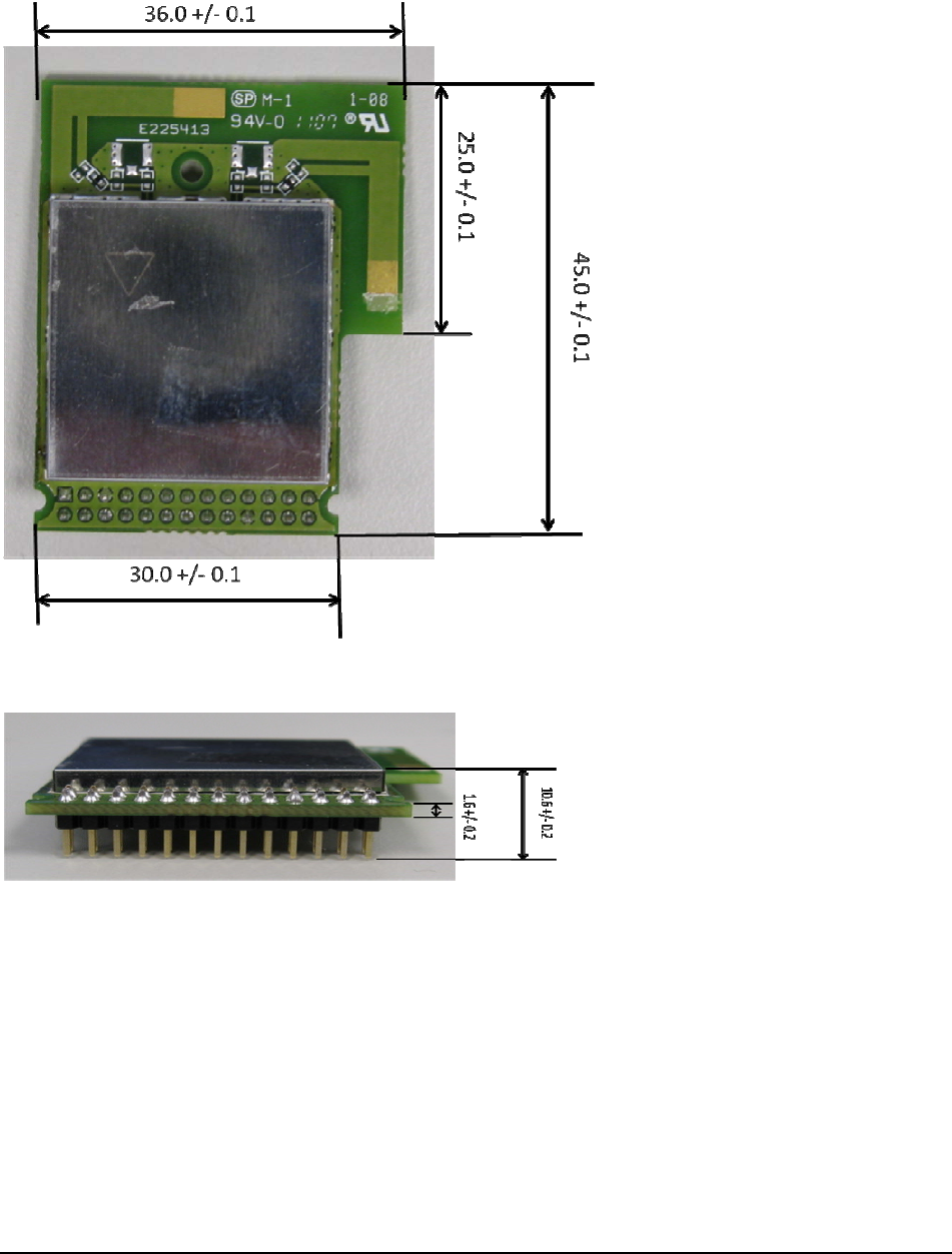
3 AVMD7300 Mechanical Dimensions
AVMD7300RX Module Datasheet PRELIMINARY v0p9
CONTENTS SUBJECT TO CHANGE WITHOUT NOTICE 8 AVNERA PROPRIETARY & CONFIDENTIAL
4 Electrical Specifications
4.1 Absolute Maximum Ratings
Absolute Maximum Ratings (AMR) are stress ratings only. AMR corresponds to the maximum value that can be applied without leading
to instantaneous or very short-term unrecoverable hard failure (destructive breakdown). Stresses beyond those listed under AMR may
cause permanent damage to the device.
Functional operation of the device at these or any other conditions beyond those indicated under “Recommended Operating Range” is
not implied. Exposure to absolute-maximum-rated conditions for extended periods may adversely affect device reliability.
Device functional operating limits and guaranteed performance specifications are given under Electrical Characteristics at the test
conditions specified.
CONDITION MIN MAX
CONDITION MIN MAX
V3.3 Supply Voltage Input -0.3V 4.2V
V5.0 Supply Voltage Input -0.3V 6.0V
Input Voltage Range – Digital
Inputs -0.3V VVDDIO + 0.3V
Operating Temperature -40ºC +85ºC
Storage Temperature -40ºC +100ºC
Static Discharge Voltage – HBM* 1000V
*Terminology: HBM => ESD human body model
4.2 Recommended Operating Range
PARAMETER MIN TYP MAX UNIT
V3.3 pin voltage 3.0 3.6 V
V5.0 4.75 5.25 V
Ambient Temperature (T
A
) -20 40 ºC
4.3 Electrical Characteristics
Test Conditions: TA=+25ºC
Table 2; AVMD7300RX Electrical Characteristics
PARAMETER CONDITIONS MIN TYP MAX UNIT
RF Frequency Range 2405 2477 MHz
Range (LOS)
1
Normal range 15 m
Current consumption
(normal range) V3.3 (Active Audio Mode) 50 mA
5 Package Design
TBD

AVMD7300RX Module Datasheet PRELIMINARY v0p9
CONTENTS SUBJECT TO CHANGE WITHOUT NOTICE 9 AVNERA PROPRIETARY & CONFIDENTIAL
FCC Statement
Federal Communication Commission Interference Statement
This equipment has been tested and found to comply with the limits for a Class B digital device, pursuant to Part 15 of the FCC Rules.
These limits are designed to provide reasonable protection against harmful interference in a residential installation. This equipment
generates, uses and can radiate radio frequency energy and, if not installed and used in accordance with the instructions, may cause
harmful interference to radio communications. However, there is no guarantee that interference will not occur in a particular installation. If
this equipment does cause harmful interference to radio or television reception, which can be determined by turning the equipment off
and on, the user is encouraged to try to correct the interference by one of the following measures:
● Reorient or relocate the receiving antenna.
● Increase the separation between the equipment and receiver.
● Connect the equipment into an outlet on a circuit different from that to which the receiver is connected.
● Consult the dealer or an experienced radio/TV technician for help.
FCC Caution: Any changes or modifications not expressly approved by the party responsible
for compliance could void the user’s authority to operate this equipment.
This device complies with Part 15 of the FCC Rules. Operation is subject to the following two conditions: (1) This device may not cause
harmful interference, and (2) this device must accept any interference received, including interference that may cause undesired
operation.
This device and its antenna(s) must not be co-located or operation in conjunction with any other antenna or transmitter.
Any changes or modifications not expressly approved by the manufacturer could void the user's authority to operate this equipment.
USERS MANUAL OF THE END PRODUCT:
The end user has to be informed that the FCC radio-frequency exposure guidelines for an uncontrolled environment can be satisfied. The
end user has to also be informed that any changes or modifications not expressly approved by the manufacturer could void the user's
authority to operate this equipment. If the size of the end product is smaller than 8x10cm, then additional FCC part 15.19 statement is
required to be available in the users manual: This device complies with Part 15 of FCC rules. Operation is subject to the following two
conditions: (1) this device may not cause harmful interference and (2) this device must accept any interference received, including
interference that may cause undesired operation.
LABEL OF THE END PRODUCT:
The final end product must be labeled in a visible area with the following " Contains TX FCC ID: NKR-SWA8 ". If the size of the end
product is larger than 8x10cm, then the following FCC part 15.19 statement has to also be available on the label: This device complies
with Part 15 of FCC rules. Operation is subject to the following two conditions: (1) this device may not cause harmful interference and (2)
this device must accept any interference received, including interference that may cause undesired operation.

AVMD7300RX Module Datasheet PRELIMINARY v0p9
CONTENTS SUBJECT TO CHANGE WITHOUT NOTICE 10 AVNERA PROPRIETARY & CONFIDENTIAL
IC Statement
This Class B digital apparatus complies with Canadian ICES-003.
Cet appareil numérique de la classe B conforme á la norme NMB-003 du Canada.
This device complies with Industry Canada license-exempt RSS standard(s). Operation is subject to the following two conditions: (1) this
device may not cause interference, and (2) this device must accept any interference, including interference that may cause undesired
operation of the device.
Le présent appareil est conforme aux CNR d'Industrie Canada applicables aux appareils radio exempts de licence. L'exploitation est
autorisée aux deux conditions suivantes : (1) l'appareil ne doit pas produire de brouillage, et (2) l'utilisateur de l'appareil doit accepter tout
brouillage radioélectrique subi, même si le brouillage est susceptible d'en compromettre le fonctionnement.
This device and its antenna(s) must not be co-located or operation in conjunction with any other antenna or transmitter.
Any changes or modifications not expressly approved by the manufacturer could void the user's authority to operate this equipment.
USERS MANUAL OF THE END PRODUCT:
In the users manual of the end product, the end user has to be informed that the IC radio-frequency exposure guidelines for an
uncontrolled environment can be satisfied. The end user has to also be informed that any changes or modifications not expressly
approved by the manufacturer could void the user's authority to operate this equipment. IC statement is required to be available in the
users manual: This Class B digital apparatus complies with Canadian ICES-003. Operation is subject to the following two conditions: (1)
this device may not cause harmful interference and (2) this device must accept any interference received, including interference that may
cause undesired operation.
LABEL OF THE END PRODUCT:
The final end product must be labeled in a visible area with the following " Contains TX IC : 4441A-SWA8 ".