Wuerth Elektronik eiSos and Co KG AMB2220 AMB2220 User Manual Testreport ETS 300 335
Wuerth Elektronik eiSos GmbH & Co KG AMB2220 Testreport ETS 300 335
UserManual.wiki
>
Wuerth Elektronik eiSos and Co KG
>
AMB2220 User Manual
Users Manual
Navigation menu
Upload a User Manual
Namespaces
Wiki Guide
HTML
PDF
Info
Views
User Manual
Discussion / Help
Navigation
![AMB2220_MA_3_12 Page 4 of 48 Date: 05/2018 Abbreviations and abstract CS Checksum DC Duty cycle Relative frequency reservation period RF Radio frequency Describes everything relating to the wireless transmission Payload The real, non-redundant information in a frame/packet UserSettings Any relation to a specific entry in the UserSettings is marked in a special font and can be found in the respective chapter UART Universal Asynchronous Receiver Transmitter, allows to communicate with the module of a specific interface. Duty cycle Transmission time in relation of one hour 1% means, channel is occupied for 36 seconds per hour. Hexadecimal [HEX] 0xhh All numbers beginning with 0x are stated as hexadecimal numbers. All other numbers are decimal.](https://usermanual.wiki/Wuerth-Elektronik-eiSos-and-Co-KG/AMB2220/User-Guide-3865998-Page-5.png)
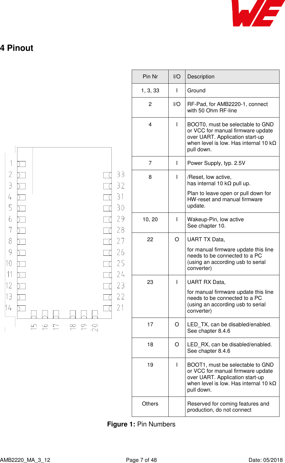
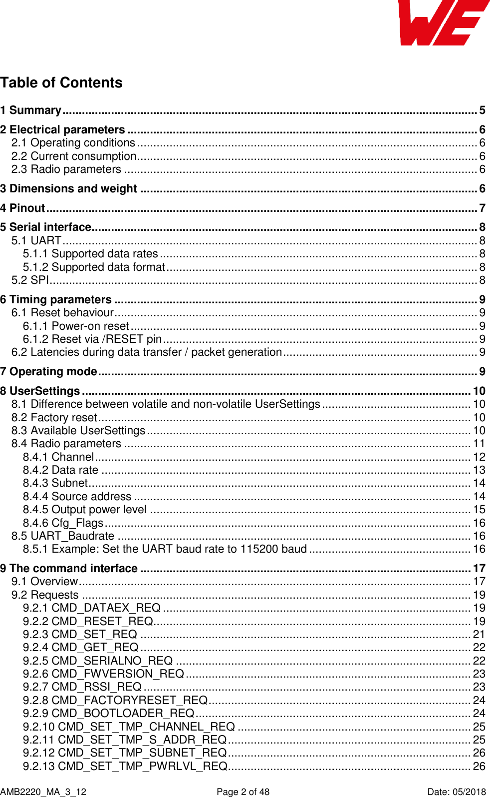
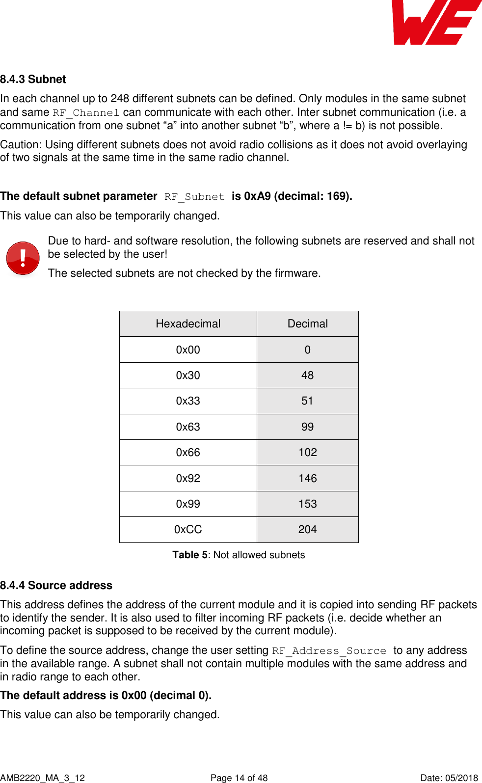
![AMB2220_MA_3_12 Page 11 of 48 Date: 05/2018 Designation Reference chapter Valid range Default value Memory position / Offset Size [bytes] RF_Channel 8.4.1 0 - 19 6 0x00 1 RF_Rate 0 1 - 7 1 0x01 1 RF_Subnet 0 1 - 255 169 0x02 1 RF_Address_Source 8.4.4 0 - 255 0 0x03 1 RF_Power_Level 0 0 - 10 10 0x04 1 Cfg_Flags 8.4.6 0 - 255 9 0x05 1 UART_Baudrate 8.5 300 - 115200 9600 0x3C 4 Table 1: Overview of non-volatile UserSettings (all values are decimal) 8.4 Radio parameters The behaviour of the radio transmitter / receiver can be influenced by selecting and/or changing RF-parameters which can be stored permanently or temporarily. User setting Description Reference chapter RF_Channel Operating channel 8.4.1 RF_Rate Data rate over RF 8.4.2 RF_Subnet Division of available channels 8.4.3 RF_Address_Source Address of current module 8.4.4 RF_Power_Level Output power level 8.4.5 Table 2: Radio parameters description overview The radio parameters must be chosen with caution, as they may influence conformity and/or performance. That the AMB2220 is certified means, that measured on the EV-Board all requirements of the corresponding norms (see chapter 18.2) are met. However decisive for the end product is the real radiated power. Using the RF-pad with an external antenna it is obvious, that the radiated power depends on the selected antenna and the wiring toward, and that it is not implemented in the certification of the AMB2220. But also for the on-board chip antenna the radiated output power is influenced by the surroundings, especially metal, and also by the quality of the power supply and possible disturbances. So it has to be pointed out, that certification does only apply for the module itself, the conformity of the end product must be stated by the manufacturer of the end-product. The frequency channels of the module can be selected from a 4 MHz raster. All channels can be used by parallel networks, as they are not overlapping, see Figure 2. Off course](https://usermanual.wiki/Wuerth-Elektronik-eiSos-and-Co-KG/AMB2220/User-Guide-3865998-Page-12.png)
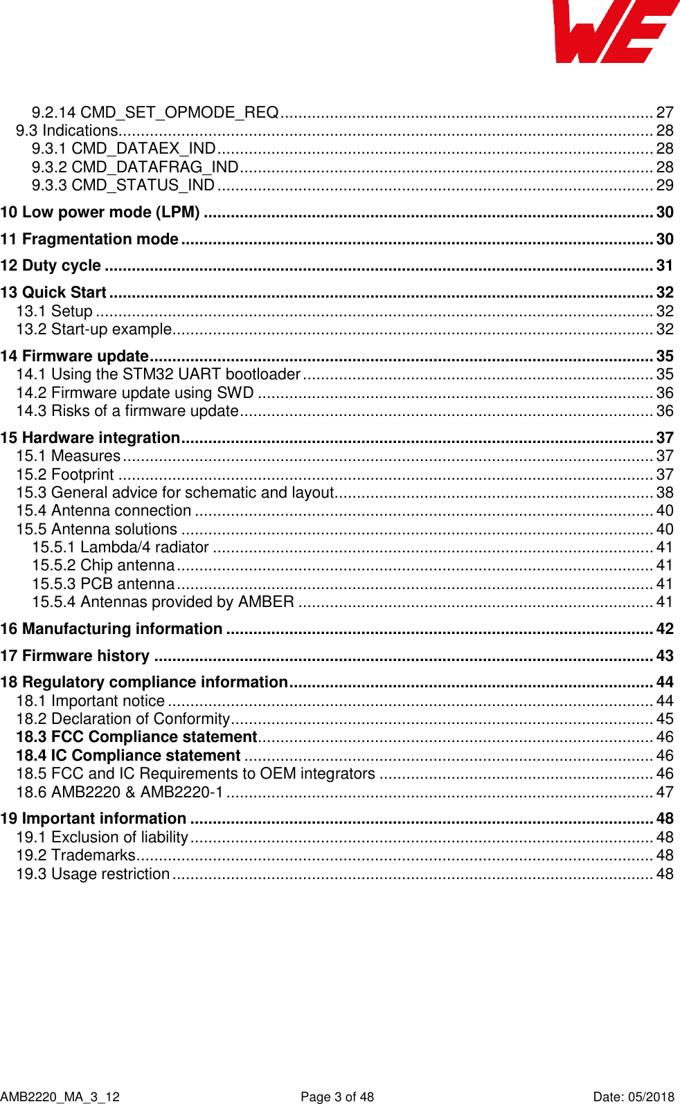
![AMB2220_MA_3_12 Page 13 of 48 Date: 05/2018 Band Channel Frequency RF_Channel [MHz] 2400 MHz – 2483.5 MHz output power ≤ 10 dBm channel separation ≤ 4 MHz 0 2401.5 1 2405.5 2 2409.5 3 2413.5 4 2417.5 5 2421.5 6 (default) 2425.5 7 2429.5 8 2433.5 9 2437.5 10 2441.5 11 2445.5 12 2449.5 13 2463.5 14 2457.5 15 2461.5 16 2465.5 17 2469.5 18 2473.5 19 2477.5 Table 3: RF Channel overview 8.4.2 Data rate Data rate [kbps] RF_Rate Sensitivity [dBm] 1.5 1 (default) -115 3 2 -113 6 3 -111 12 4 -107 24 5 -102 48 6 -98 72 7 -96 Table 4 : Selectable data rates The sensitivity in the receiver is an essential parameter for the range of the module. A lower sensitivity results in a higher range.](https://usermanual.wiki/Wuerth-Elektronik-eiSos-and-Co-KG/AMB2220/User-Guide-3865998-Page-14.png)
![AMB2220_MA_3_12 Page 15 of 48 Date: 05/2018 Remember that 0xFF (decimal 255) is the broadcast address. Any module in range on that radio channel and on that same subnet will receive this packet. 8.4.5 Output power level The output power level can be adapted through the user setting parameter RF_Power_Level. This value can also be temporarily changed. The default power level is 10 (0x0A). The given DC total current consumption includes radio IC and µC consumption. Power level RF_Power_Level Output power* [dBm] DC total current consumption [mA] 10 8.9 33.4 9 8 26.5 8 6.8 22.95 7 5.95 20.69 6 4.59 19.2 5 3.5 18.92 4 2.6 17.39 3 1.5 15.93 2 0.9 14.01 1 -0.04 13.36 0 -1.14 12.65 * Measured in a cable-bound environment. Results may vary in customer application, different antennas and with different VCC values.](https://usermanual.wiki/Wuerth-Elektronik-eiSos-and-Co-KG/AMB2220/User-Guide-3865998-Page-16.png)
![AMB2220_MA_3_12 Page 23 of 48 Date: 05/2018 9.2.6 CMD_FWVERSION_REQ This command is used to request the firmware version of the module. The main version number is returned first, followed by the secondary version number and the revision number. Format: Start Signal Command Length CS 0x02 0x0C 0x00 0x0E Response: Start Signal Command | 0x40 Length Firmware Version CS 0x02 0x4C 0x03 3 Bytes 1 Byte 9.2.7 CMD_RSSI_REQ This command returns the RX level of the last received packet determined by the transceiver IC in the form of a signed two's complement. The relationship between the applied RF power, PIN at the antenna pin and the value given by the RSSI can be expressed as: PIN [dBm] = -120 dBm + RSSI byte * 8dBm , for -105 dBm < PIN < -60 dBm If no packet was received yet the return value will be 0x00. Due to this, the RSSI level has a resolution of 8 dBm. The accuracy of the RSSI is not guaranteed, and is provided for test purpose only. Format: Start Signal Command Length CS 0x02 0x0D 0x00 0x0F Response: Start Signal Command | 0x40 Length RSSI CS 0x02 0x4D 0x01 1 Byte 1 Byte](https://usermanual.wiki/Wuerth-Elektronik-eiSos-and-Co-KG/AMB2220/User-Guide-3865998-Page-24.png)
![AMB2220_MA_3_12 Page 28 of 48 Date: 05/2018 9.3 Indications 9.3.1 CMD_DATAEX_IND This indication occurs when a valuable radio packet has been received, successfully processed and assigned. It returns all information of the RF packet. No validation from the host is needed. This indication represents the opposite of CMD_DATAEX_REQ. The received RSSI byte has to be interpreted as followed: PIN [dBm] = -120 dBm + RSSI byte * 8dBm , for -105 dBm < PIN < -60 dBm Due to restrictions of the RF chip, the RSSI level has a resolution of 8 dBm. The field Addr. Source contains the source address from the radio frame, that was selected by the sender of this frame. Format: Start Signal Command Payload Length + 2 Addr. Source Payload RSSI CS 0x02 0x81 1 Byte 1 Byte Payload Length 1 Byte 1 Byte 9.3.2 CMD_DATAFRAG_IND This indication occurs when a valuable radio packet fragment has been received successfully. It returns the address of the sending device (Addr. Source), the sequence number of the RF packet, the fragment number of the current RF packet and the fragment number of the last RF packet that has to be received to complete the full RF packet. This message can enabled or disabled using the Cfg_Flags. The full RF packet is indicated using the CMD_DATAEX_IND as soon as the last packet fragment has been received. Format: Start Signal Command Length Addr. Source Sequence Number Fragment Number Number of last Fragment CS 0x02 0x82 0x04 1 Byte 1 Byte 1 Byte 1 Byte 1 Byte If a CMD_DATAFRAG_IND has been received, we strongly recommend to wait for the packet completion before performing other actions with the module. The module reception has been completed as soon as CMD_DATAEX_IND was sent to the host or the timeout occurred. In case of error, e.g. if one or several packet fragments have been lost during transmission and thus no CMD_DATAEX_IND was sent, the module reverts to operate in normal mode after 500ms.](https://usermanual.wiki/Wuerth-Elektronik-eiSos-and-Co-KG/AMB2220/User-Guide-3865998-Page-29.png)
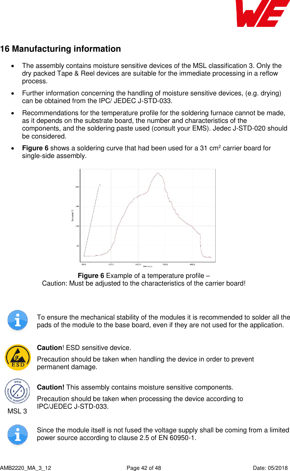
![AMB2220_MA_3_12 Page 31 of 48 Date: 05/2018 12 Duty cycle The fragmentation mode allows the transmission of larger data packets over RF. Thus there is an increased risk of exceeding the duty cycle, if existent. The time [s] the channel is blocked when sending a complete packet containing bytes using the data rate [kbps] can be calculated as: A packet with maximum size of 240 bytes would need 2.13 s, when sending it in fragmentation mode using the lowest data rate of 1.5 kbps. This means, with a duty cycle of 1% (36s per hour), only 16 packets of maximum size could be sent without violation of the duty cycle restrictions.](https://usermanual.wiki/Wuerth-Elektronik-eiSos-and-Co-KG/AMB2220/User-Guide-3865998-Page-32.png)
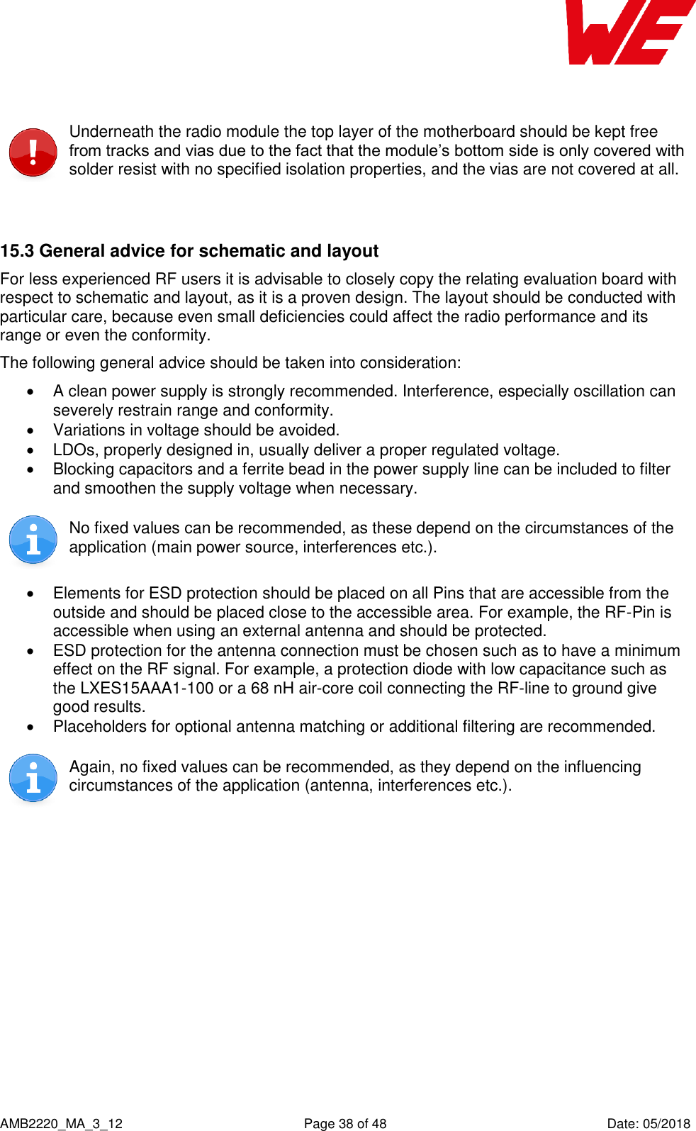
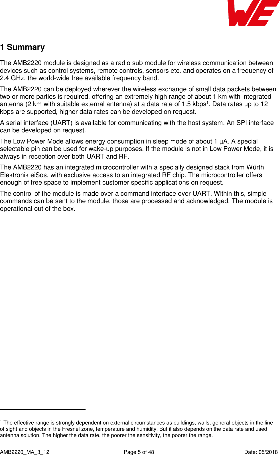
![AMB2220_MA_3_12 Page 37 of 48 Date: 05/2018 15 Hardware integration 15.1 Measures Figure 3: Dimensions [mm] 15.2 Footprint Figure 4: Footprint [mm] To avoid the risk of short circuits between VCC (or signal lines) and GND, a minimum clearance of at least 14 mm between the opposing pad rows has to be maintained respectively the pads must not be elongated underneath the module. no metal for 31mm from edge](https://usermanual.wiki/Wuerth-Elektronik-eiSos-and-Co-KG/AMB2220/User-Guide-3865998-Page-38.png)