Wuerth Elektronik eiSos and Co KG AMB9626 AMB9626 User Manual Testreport ETS 300 335
AMBER Wireless GmbH AMB9626 Testreport ETS 300 335
UserManual.wiki
>
Wuerth Elektronik eiSos and Co KG
>
AMB9626 User Manual
Users Manual
Navigation menu
Upload a User Manual
Namespaces
Wiki Guide
HTML
PDF
Info
Views
User Manual
Discussion / Help
Navigation
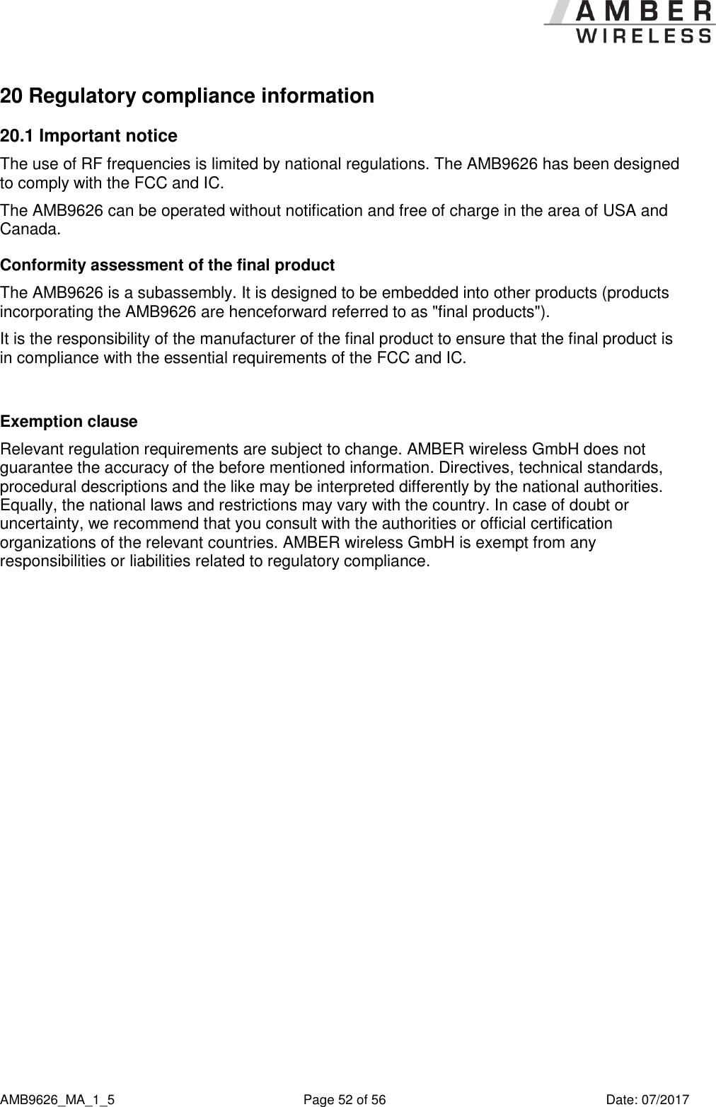
![AMB9626_MA_1_5 Page 5 of 56 Date: 07/2017 Abbreviations and abstract ACK Acknowledgement Acknowledgement pattern confirming the reception of the transmitted data package CS Checksum Checksum of the respective hex array DC Duty cycle Relative frequency reservation period LPM Low power mode Operation mode for efficient power consumption, suited for battery powered devices RF Radio frequency Describes everything relating to the wireless transmission or reception PL Payload The real, non-redundant information in a frame/packet US User settings Any relation to a specific entry in the user settings is marked in a special font and can be found in the respective chapter UART Universal Asynchronous Receiver Transmitter This function allows the Host to communicate with the module over a specified interface. DC Duty cycle Transmission time in relation of one hour e.g. 1% means, channel is occupied for 36 seconds per hour, 0.1% means 3.6 seconds per hour. [HEX] 0xhh Hexadecimal All numbers beginning with 0x are stated as hexadecimal numbers. All other numbers are decimal.](https://usermanual.wiki/Wuerth-Elektronik-eiSos-and-Co-KG/AMB9626/User-Guide-3606734-Page-6.png)
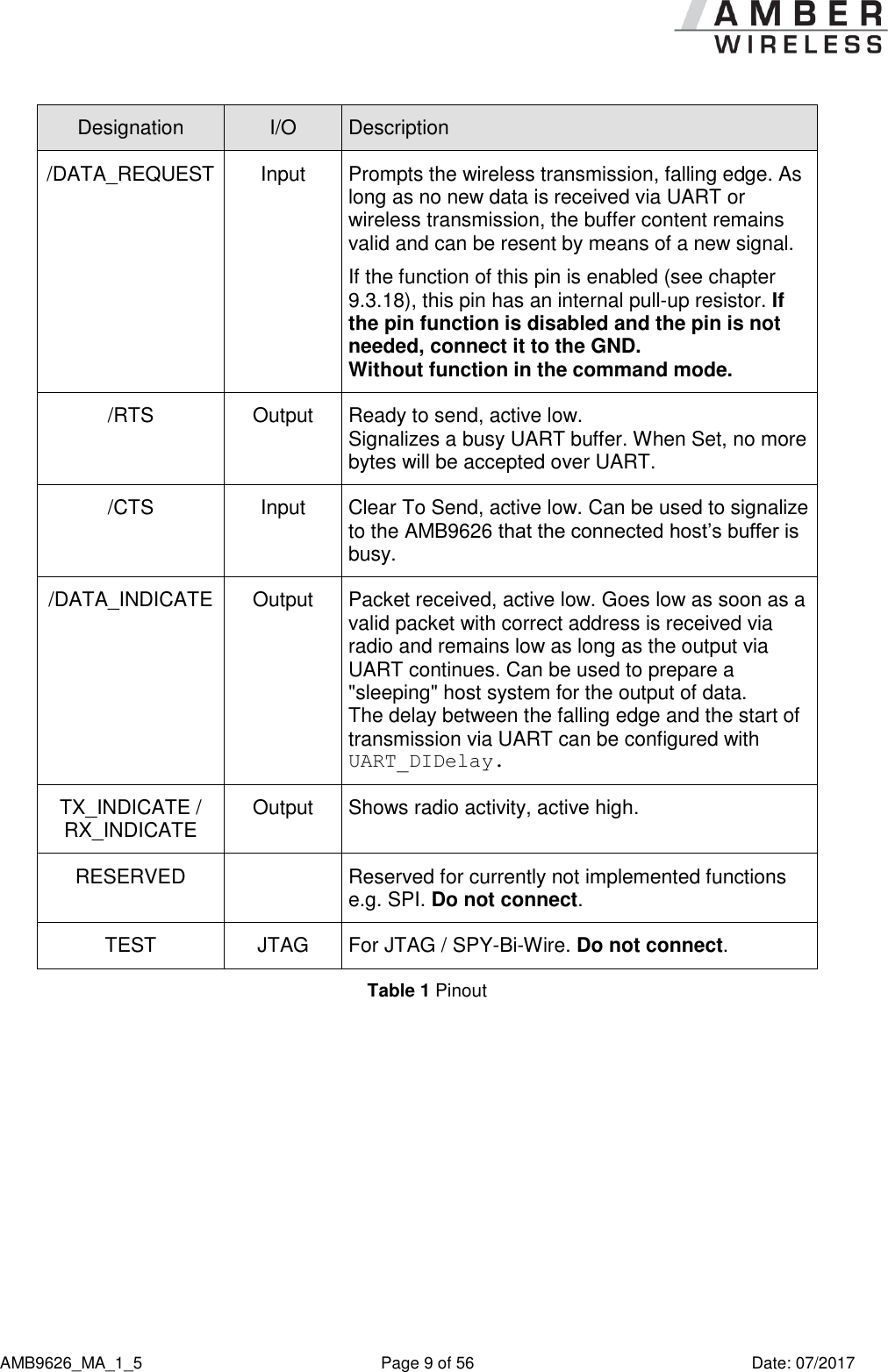
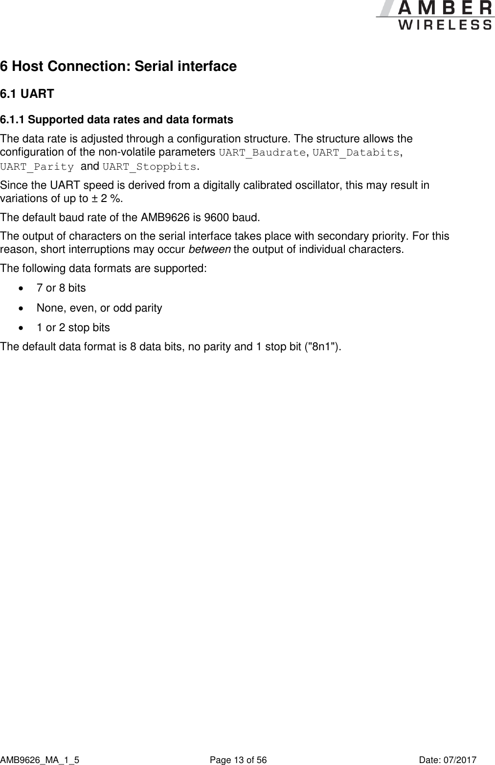
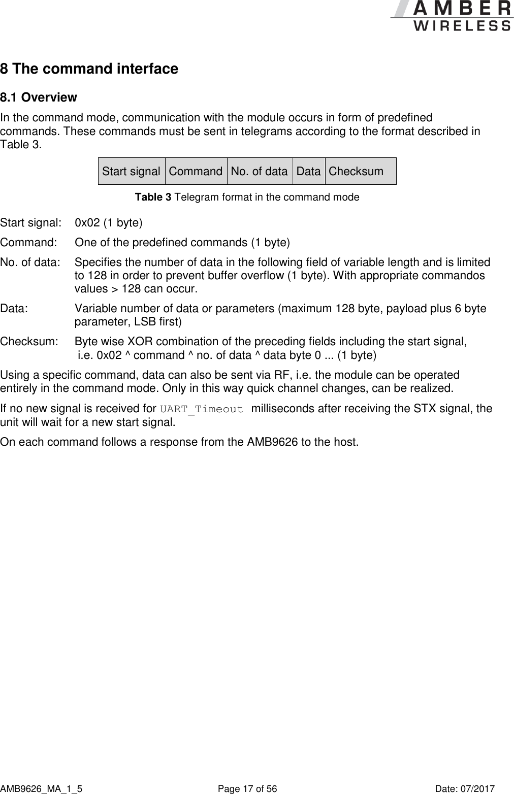
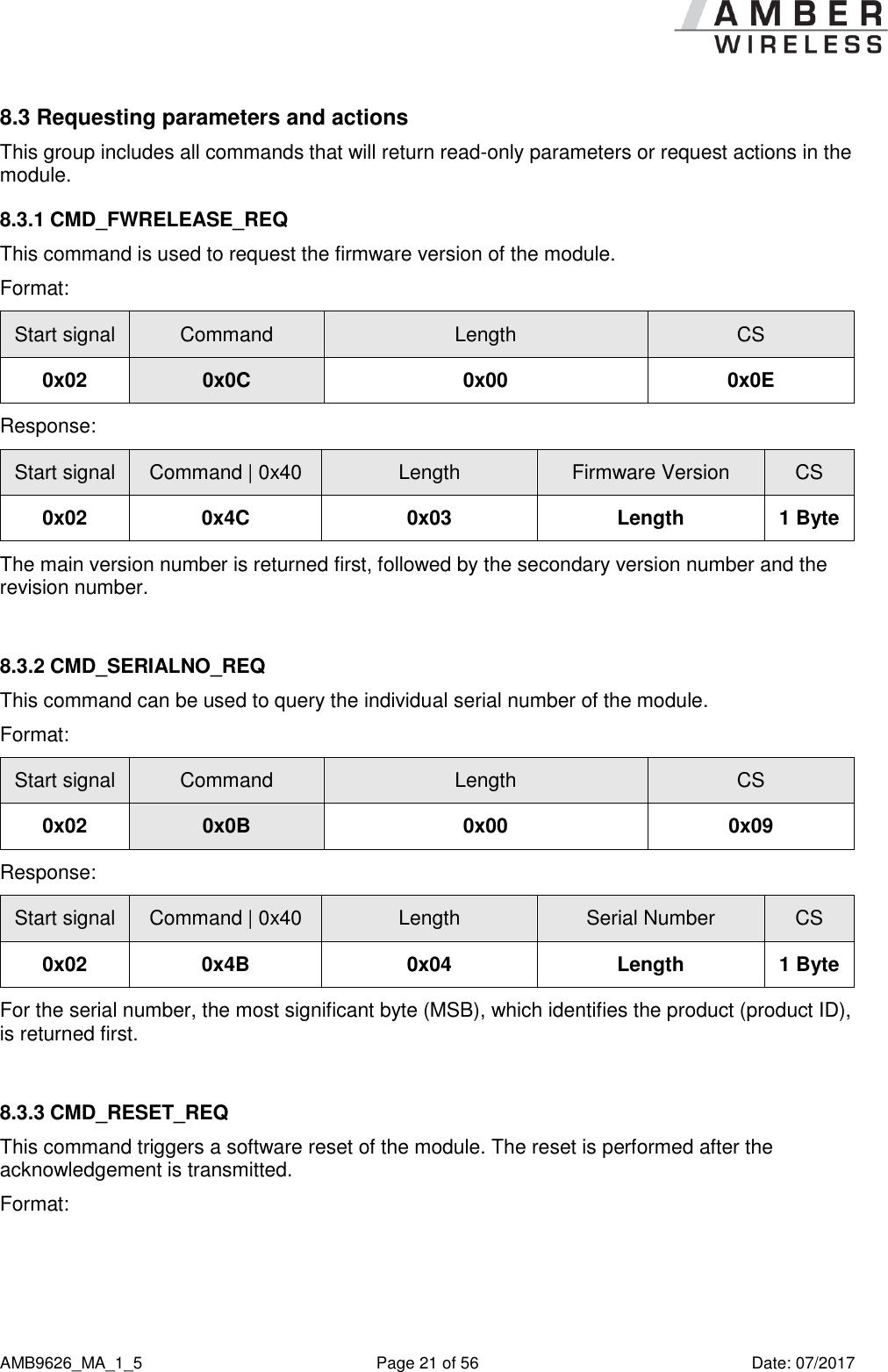
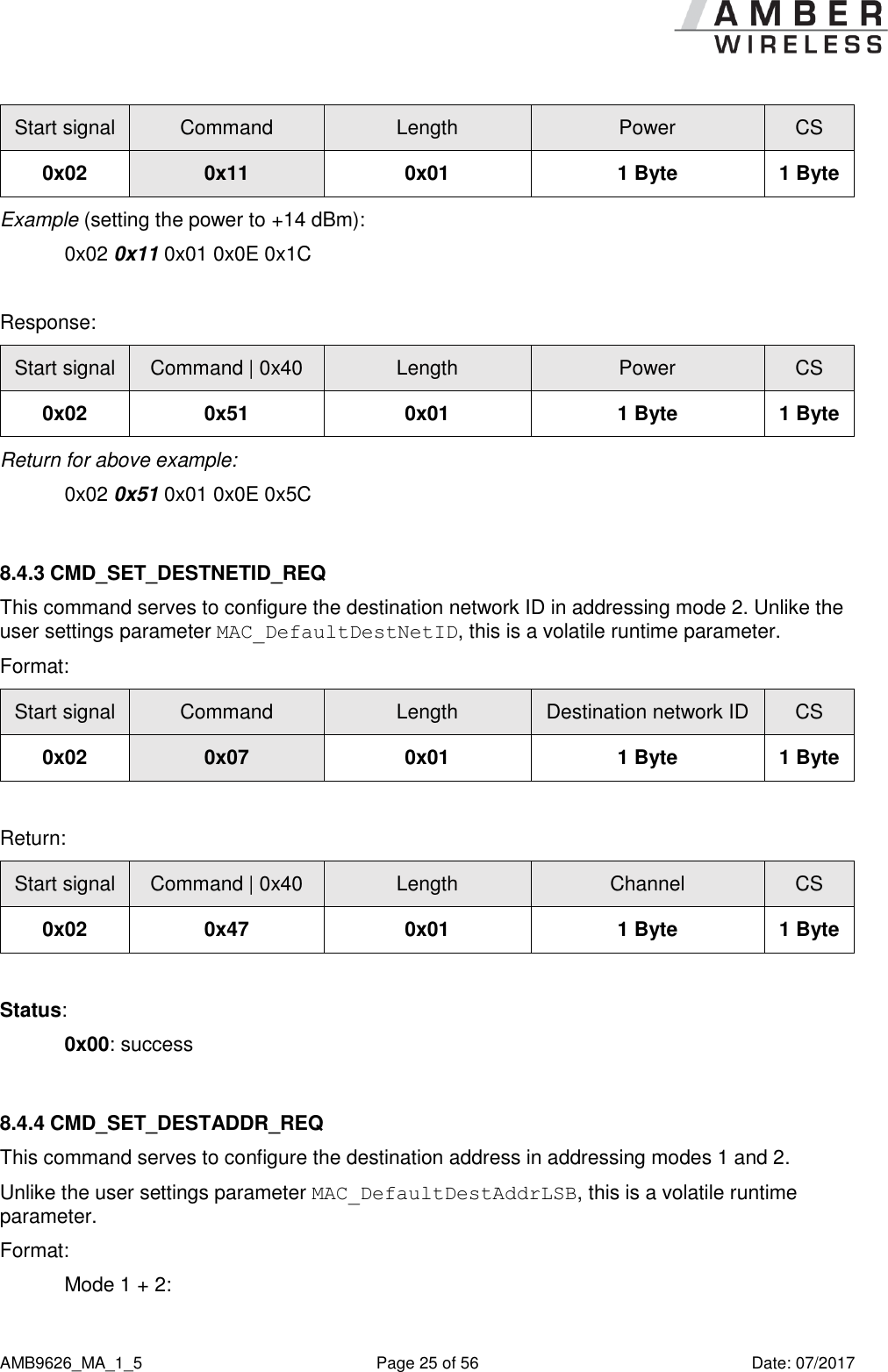
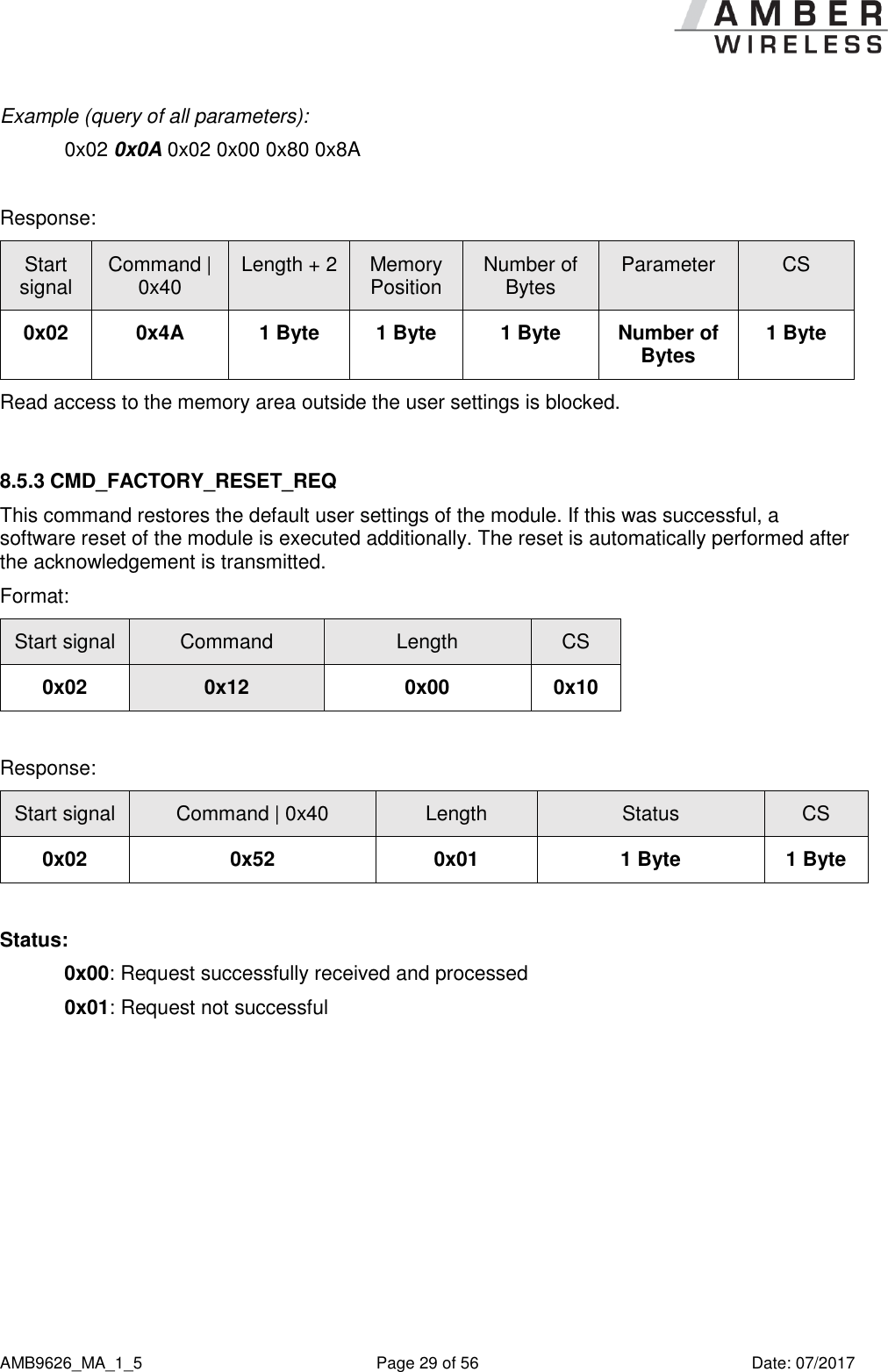
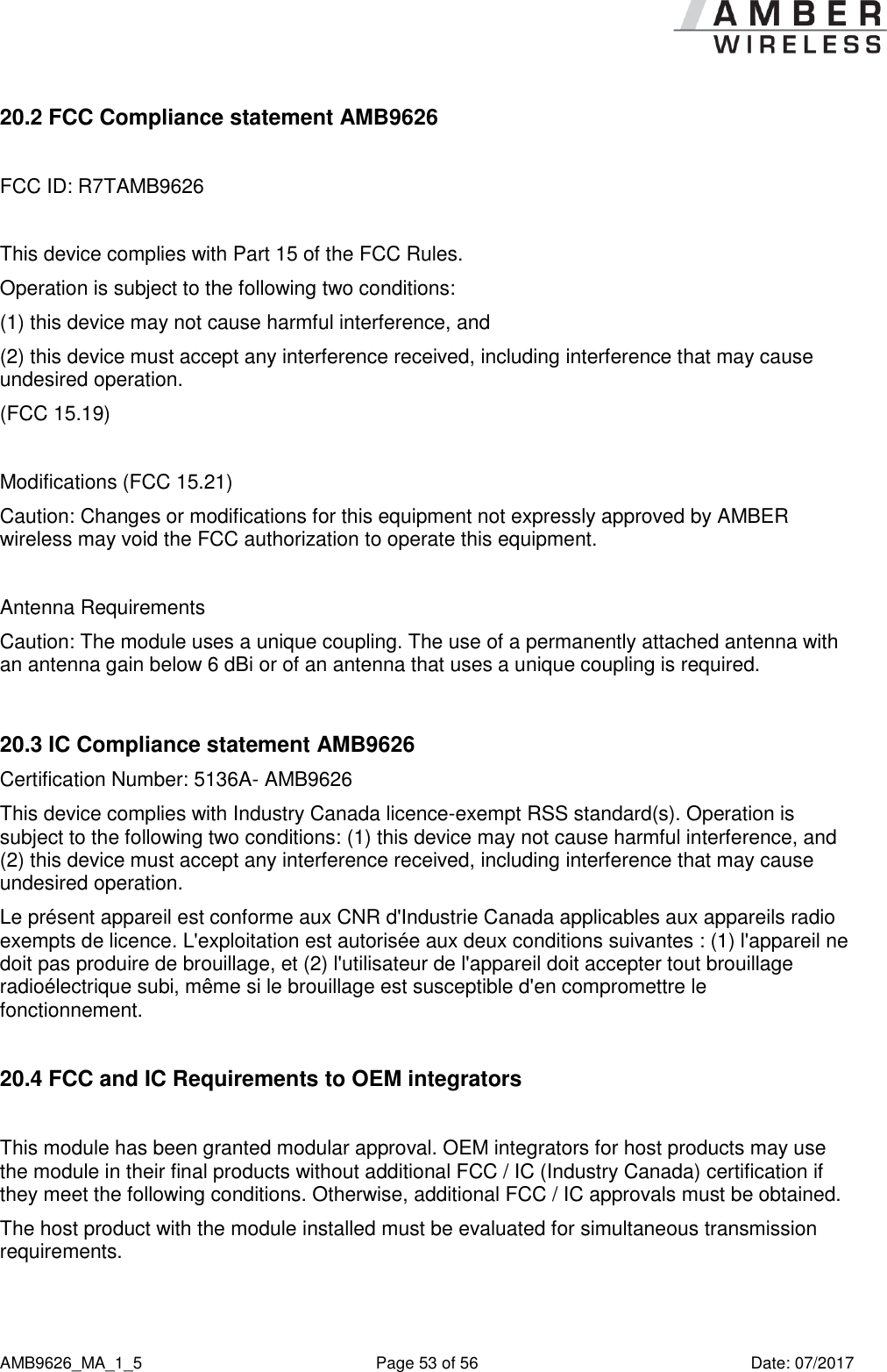
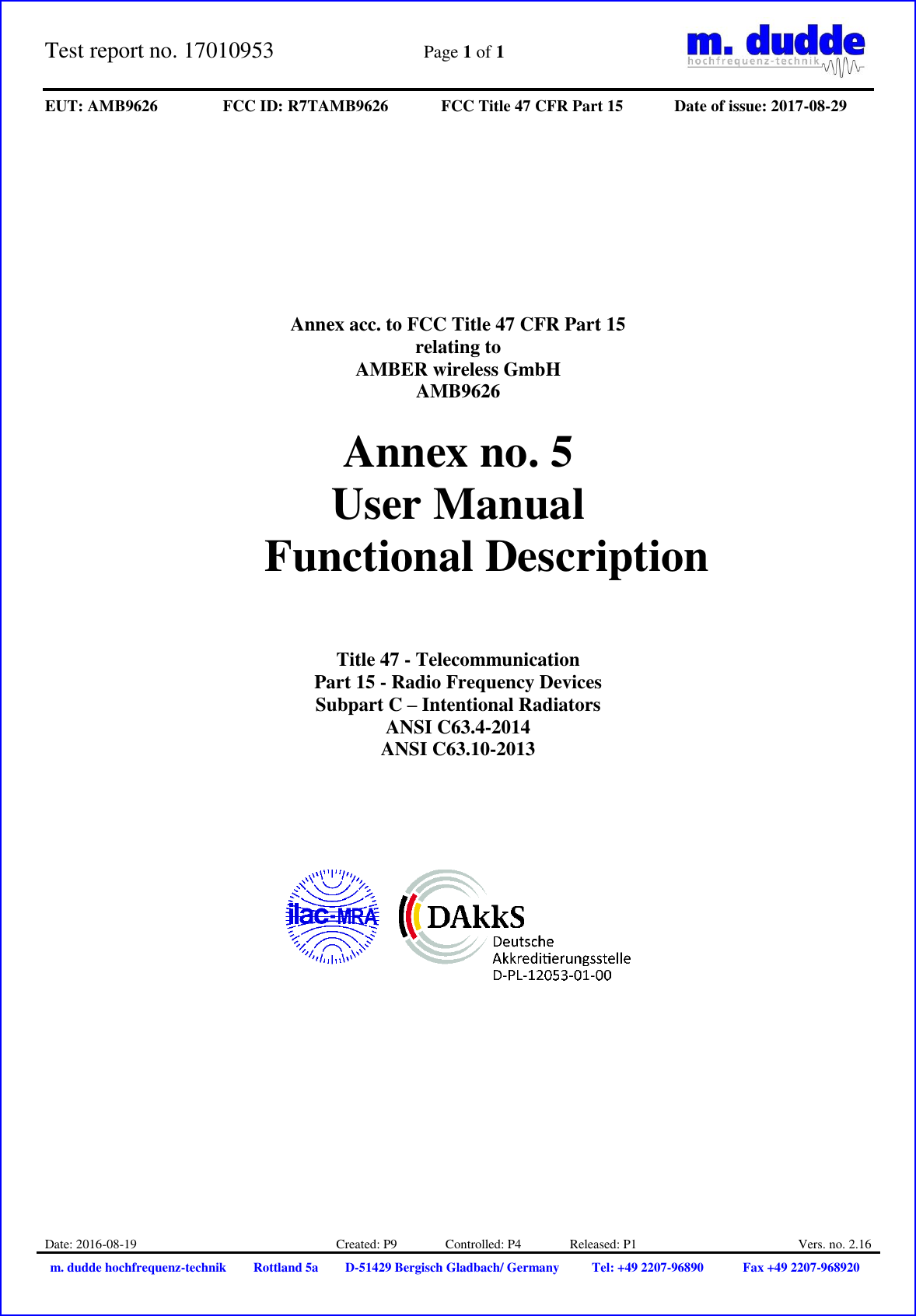
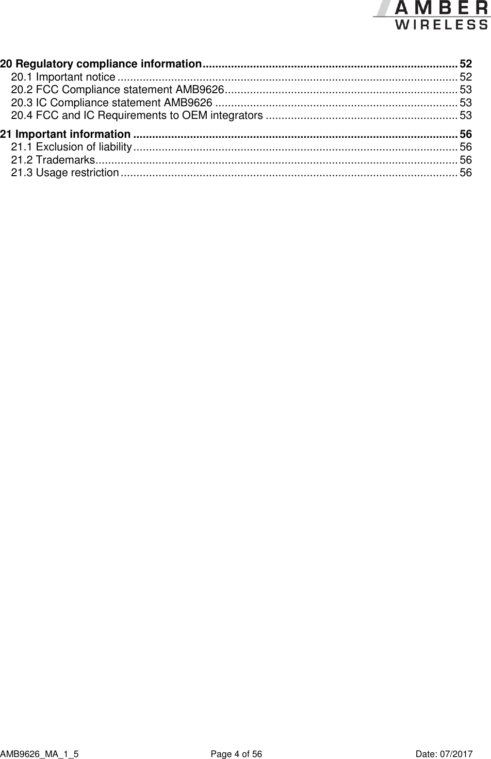
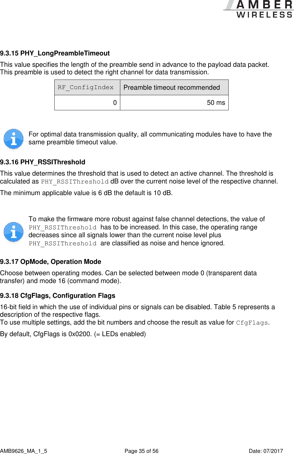
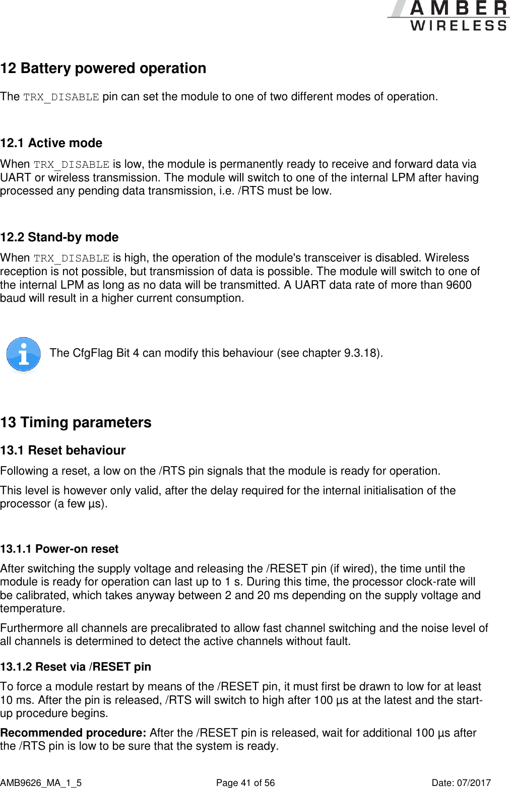
![AMB9626_MA_1_5 Page 30 of 56 Date: 07/2017 9 User settings 9.1 Difference between volatile and non-volatile settings The so called user settings are stored permanently into the internal flash of the module. At start-up, these user settings are loaded into volatile settings, so called runtime settings. The validation of these runtime settings is lost after the module is powered off, or restarted (the process starts over again). 9.2 List of user settings The non-volatile user settings listed in the following table can be modified by means of specific commands in the configuration mode (CMD_SET_REQ) of the module or by using the Windows software "ACC V3". These parameters are stored permanently in the module's flash memory. All settings are described on the following pages. After changing those parameters, a reset will be necessary to make use of the new settings. The validity of the specified parameters is not verified. Incorrect values can result in device malfunction! Designation Summary Permissible values Default value Memory position Number of bytes UART_PktMode Packetizing mode Selects the packet generation method 0 or 1 0 5 1 UART_PktSize Packet size Number of characters for transmission start with set packet size 1 - 120 120 7 1 UART_RTSLimit /RTS limit Number of received characters after which /RTS responds 1 - 120 100 8 1 UART_ETXChar ETX character End-of-text character used to mark data packets; reception of this character triggers wireless transmission 0 - 255 10 9 1 UART_Timeout Timeout Timeout after the last character before the data received via UART are transmitted via wireless transmission [ms] 2 – 65535 5 12 2 UART_DIDelay Data Indication Delay Delay between signal by Pin /DATA_INDICATION and beginning of output by UART [ms] 0 – 65535 0 14 2 MAC_NumRetrys Retries Number of wireless retries, 0: retrys disabled 0 – 255 0 20 1](https://usermanual.wiki/Wuerth-Elektronik-eiSos-and-Co-KG/AMB9626/User-Guide-3606734-Page-31.png)
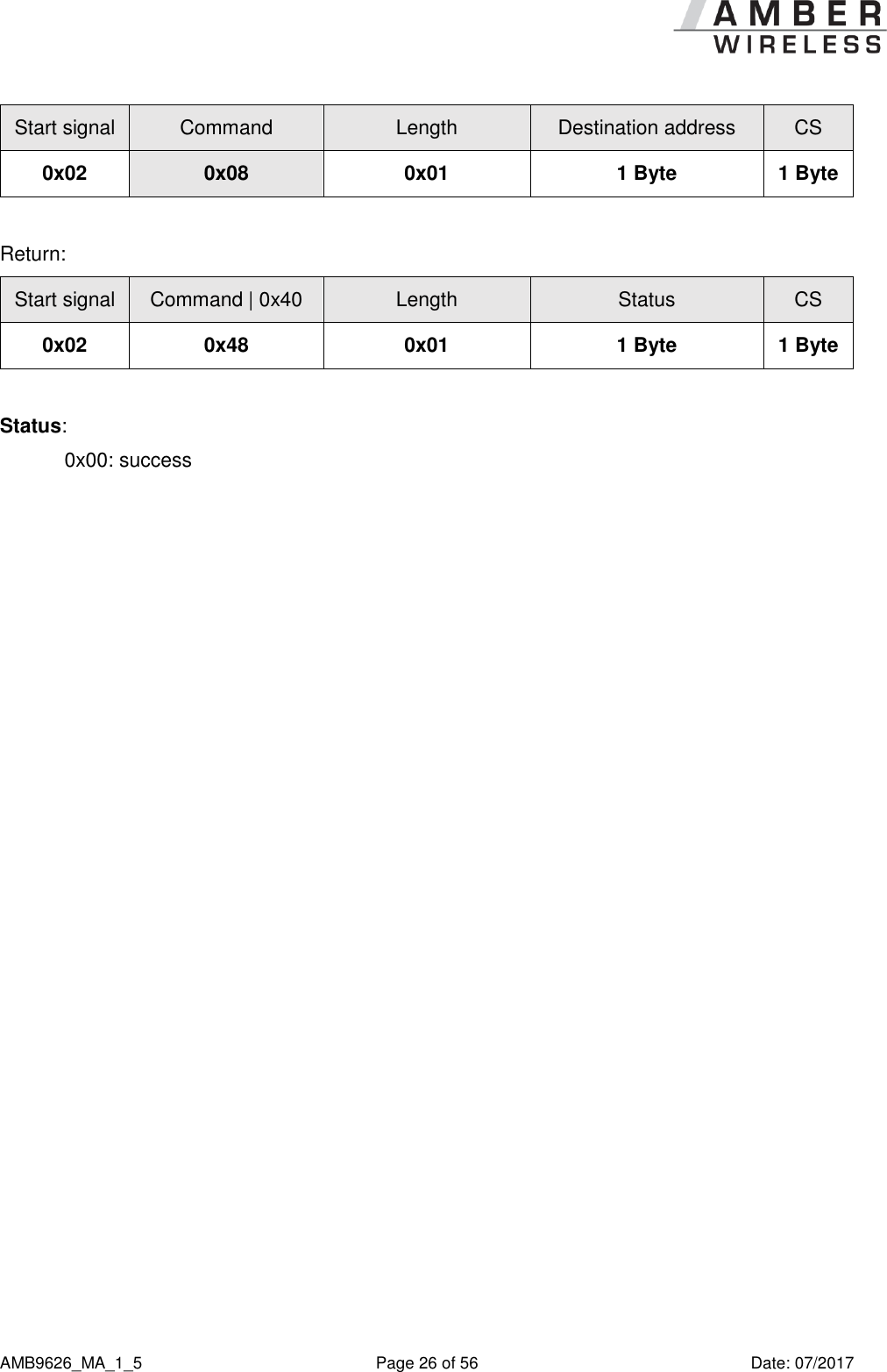
![AMB9626_MA_1_5 Page 31 of 56 Date: 07/2017 Designation Summary Permissible values Default value Memory position Number of bytes MAC_AddrMode Addressing mode Wireless Addressing mode 0/1/2 0 21 1 MAC_DefaultDestNetID Dest. net ID Default destination network ID 0 – 255 0 24 1 MAC_DefaultDestAddrLSB Dest. device address Default destination address (LSB) 0 – 255 0 25 1 MAC_DefaultSourceNetID Local net ID Own network ID 0 – 254 0 28 1 MAC_DefaultSourceAddrLSB Local device address Own address (LSB) 0 – 255 0 29 1 MAC_ACKTimeout ACK timeout Waiting time for wireless acknowledgement [ms] 5 – 65535 8 32 2 PHY_PAPower Output power Output power [dBm]; value range depends on RF configuration Format: two’s complement -11 – 15 15 41 1 PHY_LongPreambleTimeout Long preamble timeout Length of the preamble used for channel hopping [ms] 5 – 65535 50 44 2 PHY_RSSIThreshold RSSI value [dB] over noise level that determines the threshold for active channel detection 6 – 40 10 46 1 OpMode Operating mode, transparent or command mode 0, 16 0 60 1 CfgFlags Configuration flags (hex.) Flags for setting various properties; see chapter 9.3.18 0 – 65535 512 72 2 UART_Baudrate Symbol rate of the UART 1200-19200 9600 80 4 UART_Databits Number of data bits 7,8 8 84 1 UART_Parity Parity 0,1,2 0 85 1 UART_Stoppbits Stop bits 1,2 1 86 1 RF_ConfigIndex Index for predefined radio settings 0 0 92 1 Table 4 Overview of non-volatile user-settings](https://usermanual.wiki/Wuerth-Elektronik-eiSos-and-Co-KG/AMB9626/User-Guide-3606734-Page-32.png)
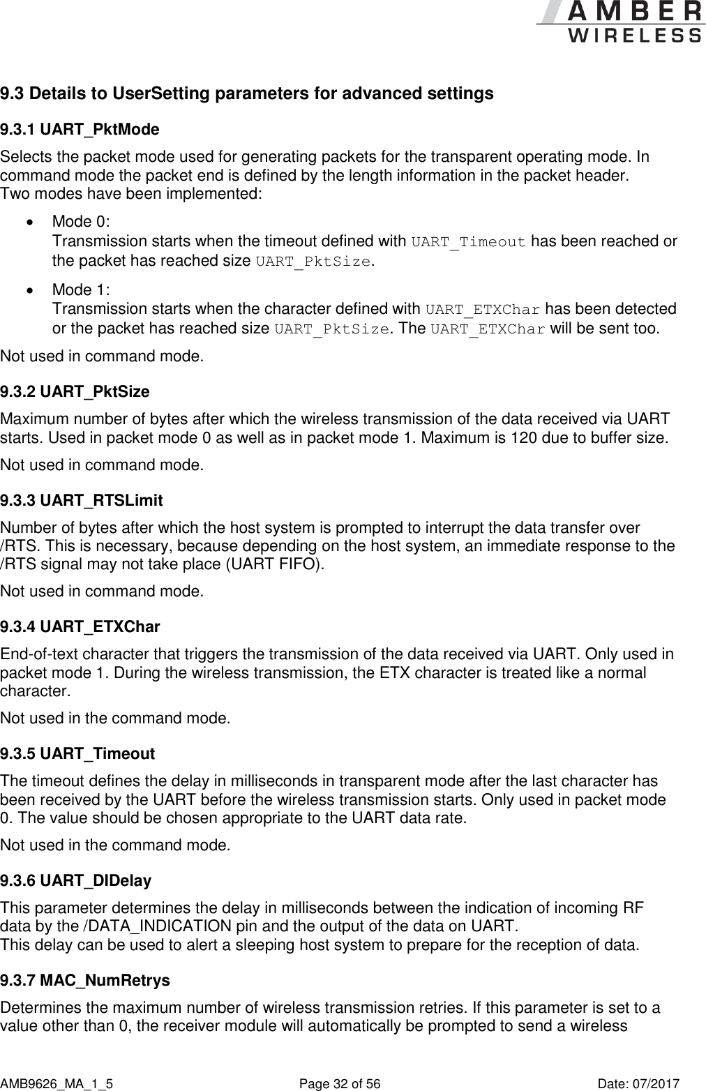
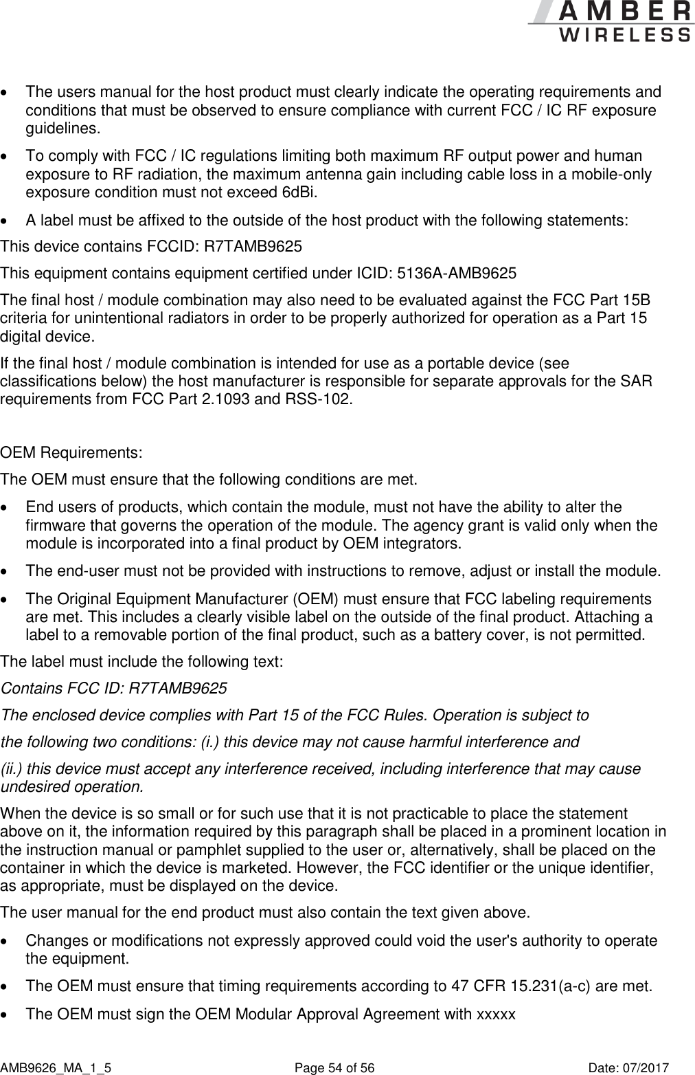
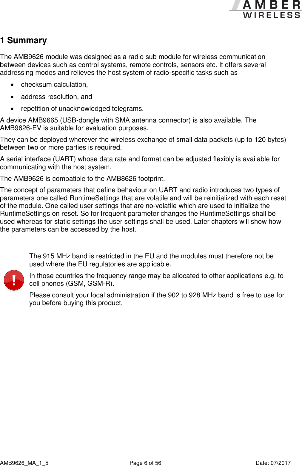
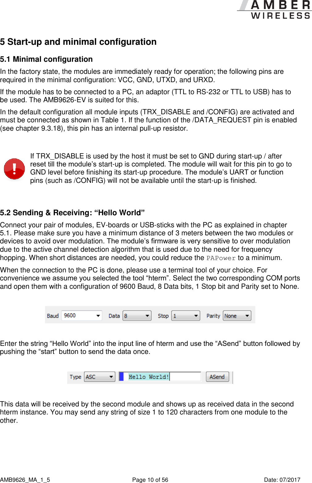
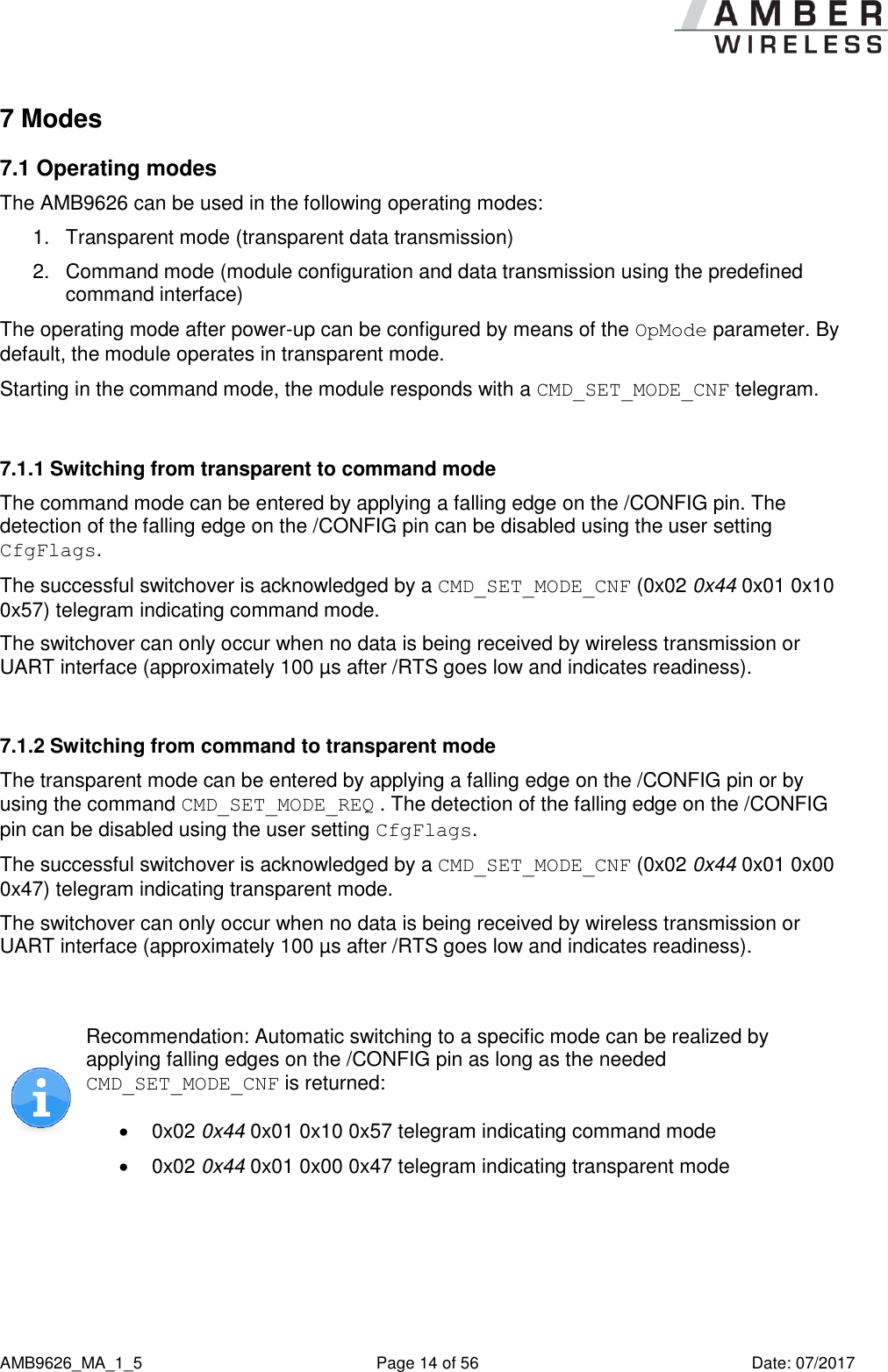
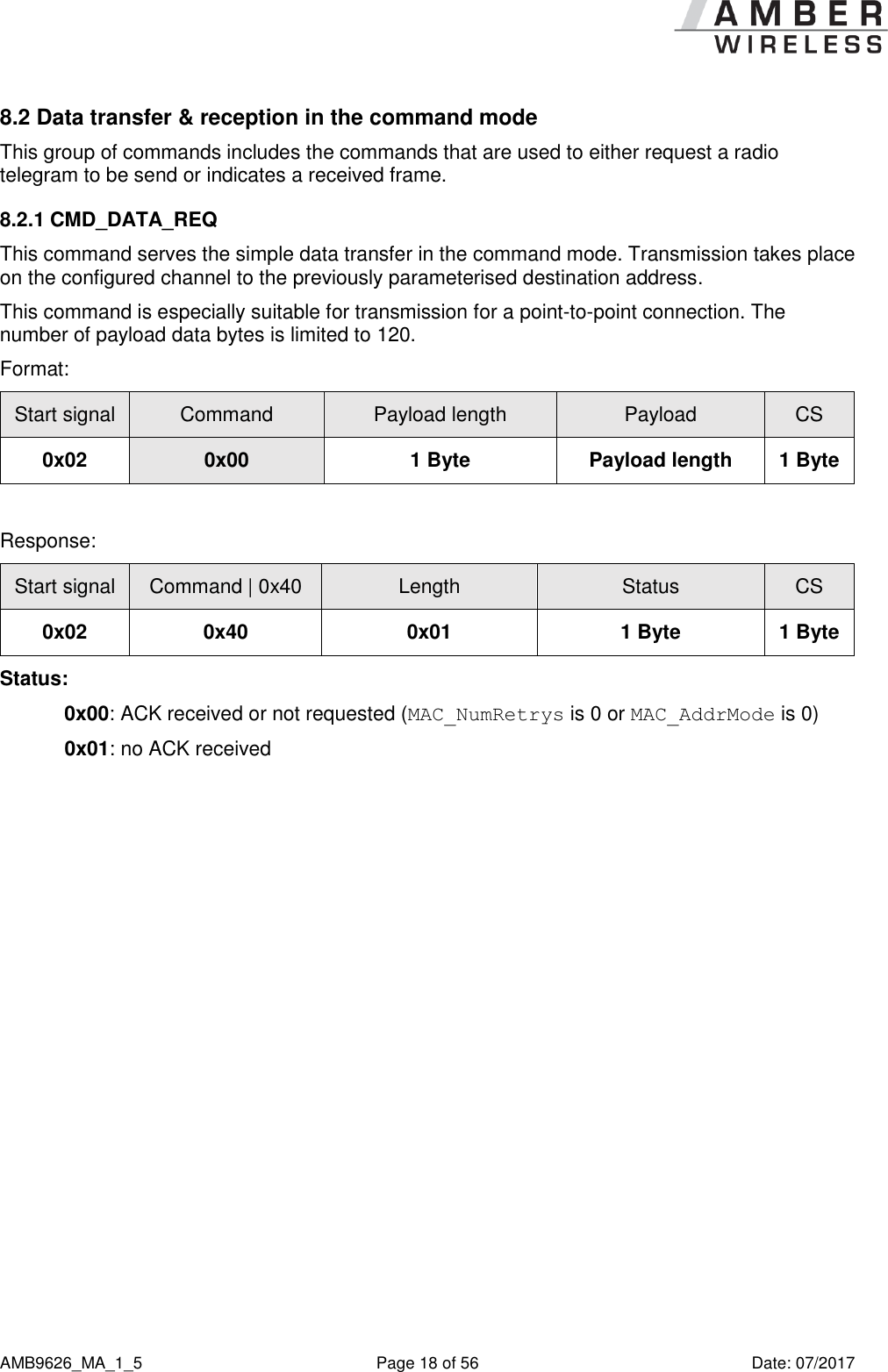
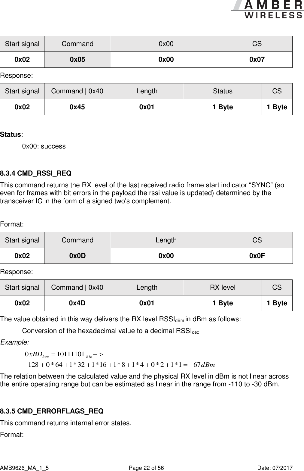
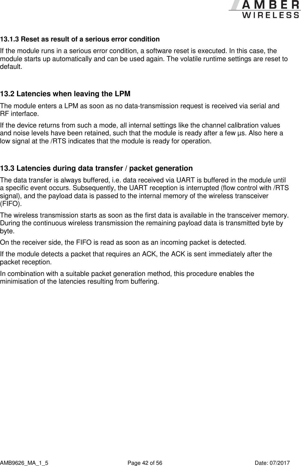
![AMB9626_MA_1_5 Page 37 of 56 Date: 07/2017 9.3.19 UART_Baudrate A 32 bit field, that contains the symbol rate for the communication interface. Symbol rates up to 19200 baud are supported. Default symbol rate is 9600 baud. Please note that for baud rates higher than 9600 baud the Sleep state has a reasonable higher energy consumption. 9.3.20 UART_Databits An 8 bit field that contains the number of data bits on the communication interface. Supported values are 7 and 8. 9.3.21 UART_Parity An 8 bit field that contains the parity for the communication interface. Values of 0 (no parity), 1 (even parity) and 2 (odd parity) are supported. 9.3.22 UART_Stoppbits An 8 bit field that contains the number of stop bits for the communication interface. Supported are 1 and 2 stop bits. 9.3.23 RF_ConfigIndex, Radio Configuration An 8 bit field that addresses the applied RF configuration. RF_ConfigIndex Data rate (gross) [kcps] Modulation 0 38.4 2-GFSK](https://usermanual.wiki/Wuerth-Elektronik-eiSos-and-Co-KG/AMB9626/User-Guide-3606734-Page-38.png)
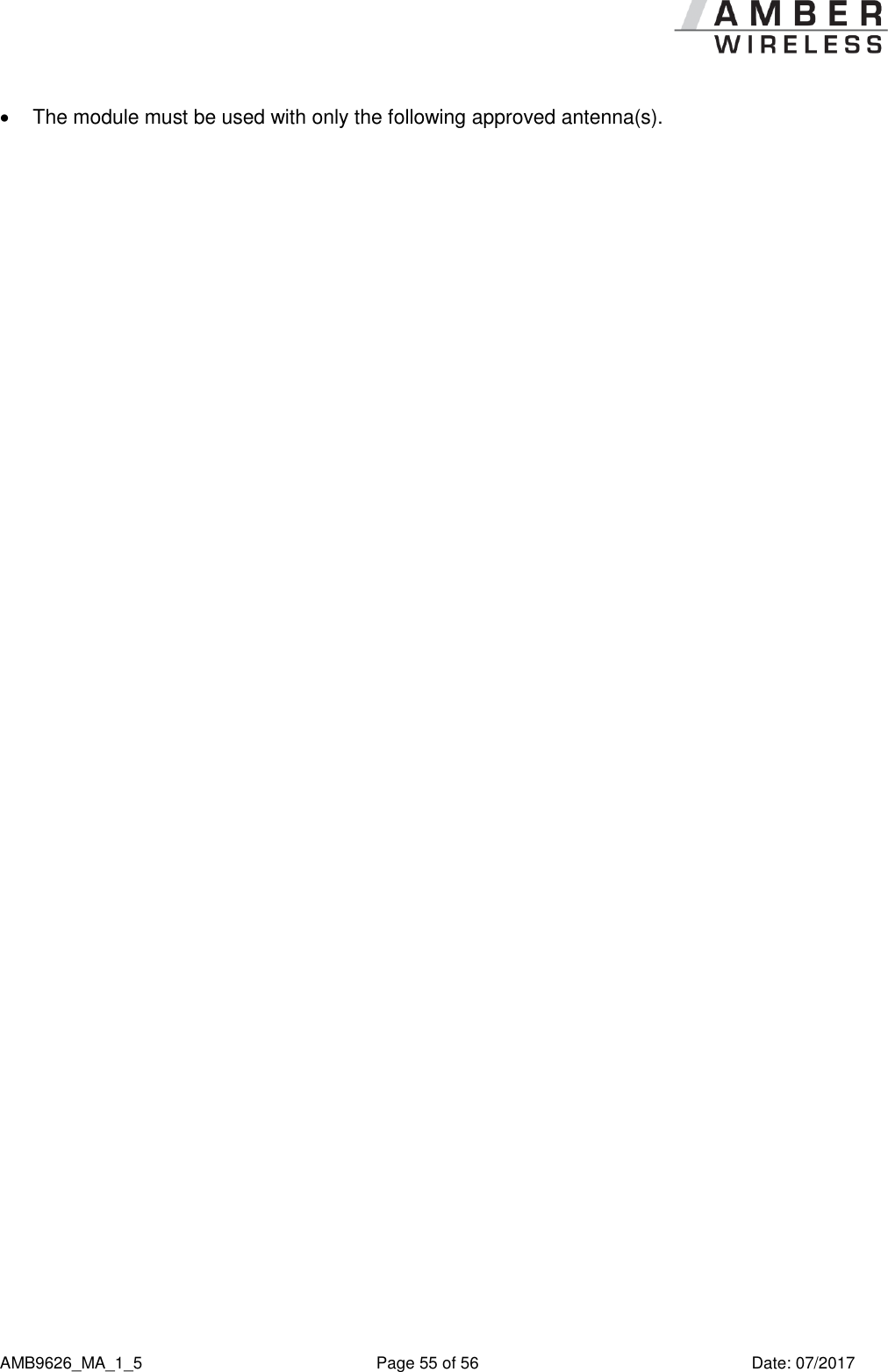
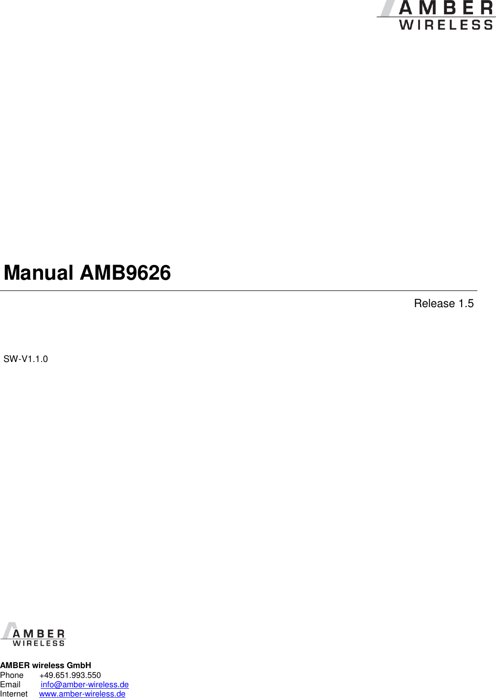
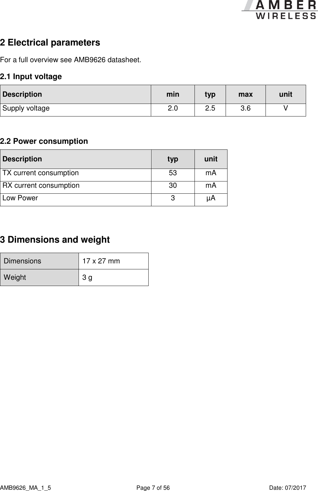
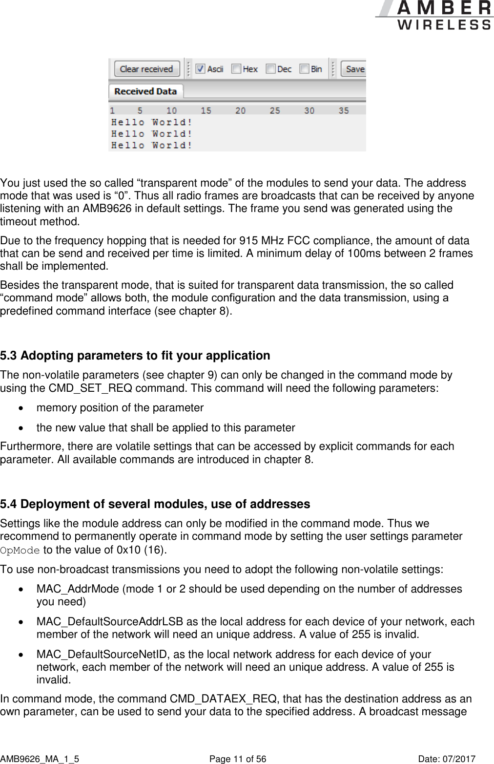
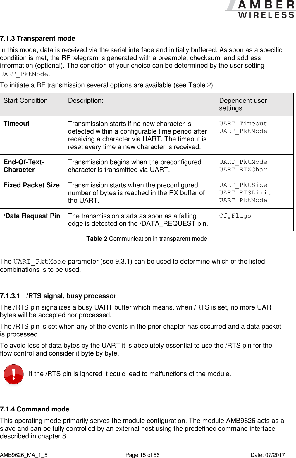
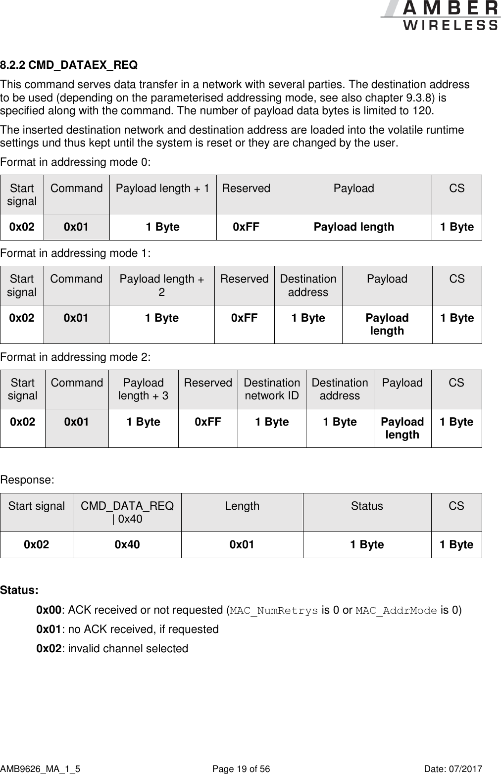
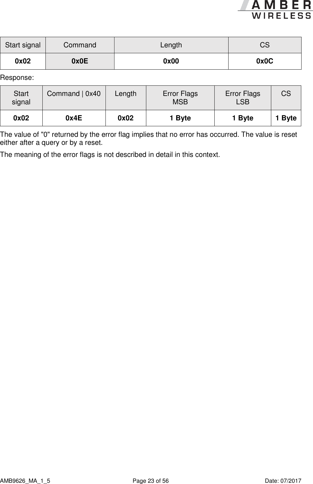
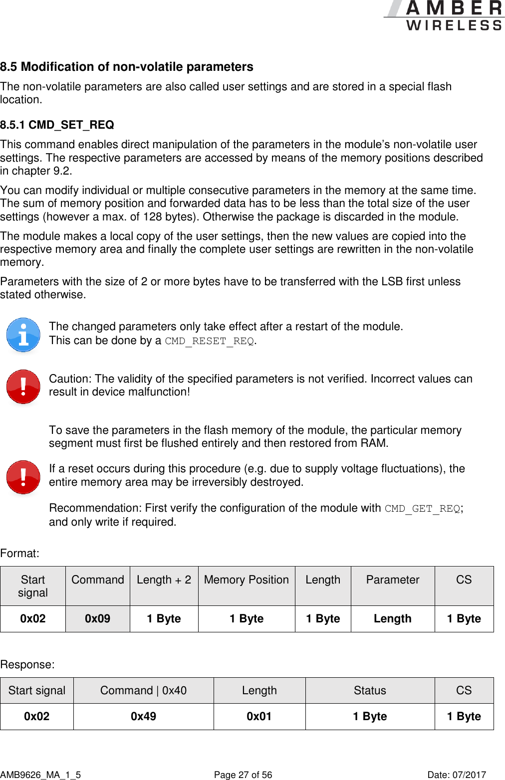
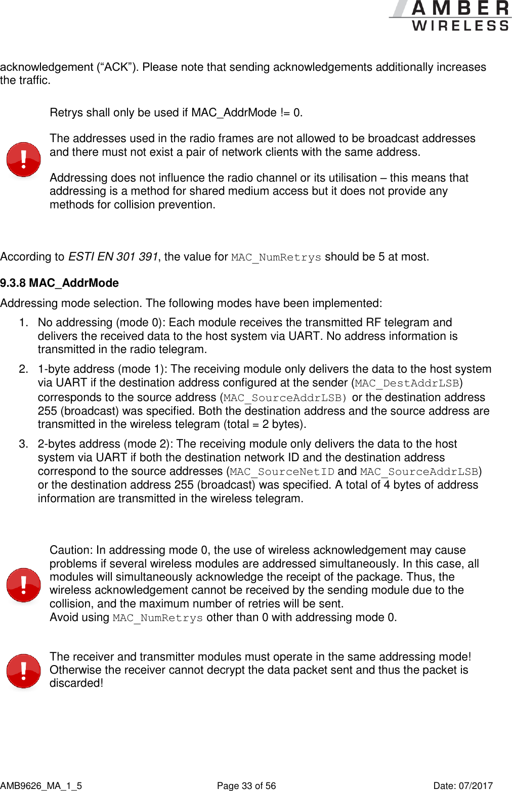
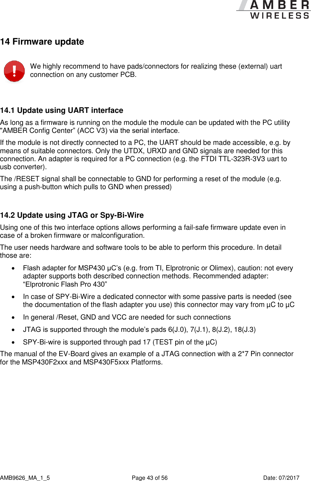
![AMB9626_MA_1_5 Page 39 of 56 Date: 07/2017 11 Channel hopping for the 915MHz frequency band The 915MHz frequency band is splitted into the channels of Table 6, where the band limit channels 200 and 252 are not to be used for any RF activity. They are chosen with equal distances of 500 kHz so that the neighbour channels should not disturb each other at the default rf data rate (38400 baud). Channel Frequency Channel Frequency Channel Frequency 200 902 218 911 236 920 201 902,5 219 911,5 237 920,5 202 903 220 912 238 921 203 903,5 221 912,5 239 921,5 204 904 222 913 240 922 205 904,5 223 913,5 241 922,5 206 905 224 914 242 923 207 905,5 225 914,5 243 923,5 208 906 226 915 244 924 209 906,5 227 915,5 245 924,5 210 907 228 916 246 925 211 907,5 229 916,5 247 925,5 212 908 230 917 248 926 213 908,5 231 917,5 249 926,5 214 909 232 918 250 927 215 909,5 233 918,5 251 927,5 216 910 234 919 252 928 217 910,5 235 919,5 Table 6 Overview of the 51 active channels according to FCC. To operate in this band the radio-norm FCC $15.247 prescribes to use all channels equally for data transmission. Thus the AMB9626 implements the so called “asynchronous channel hopping technique” [3] using a new channel for each packet send. Figure 2 illustrates exemplary the underlying idea for a frequency band consisting of 10 channels. Thereby the device in RX mode jumps quickly through the channels to listen for some RF activity. If an active channel was detected, the receiving device listens to the data packet that will follow afterwards. To find out whether a channel is active or not, the noise level of each channel is determined permanently. A channel is classified as active if its signal power is at least PHY_RSSIThreshold dB above the current noise level of the channel. Otherwise the measured value is used to update the corresponding noise level. On the TX side, the transmitting device first sends a long preamble to signalize RF activity on the chosen channel. This preamble has to be sufficiently long, that the receiver can detect the chosen channel (see the user setting PHY_LongPreambleTimeout). After this preamble was sent, the transmission of the data packet follows. For each transmission (preamble plus payload data) a new channel is chosen.](https://usermanual.wiki/Wuerth-Elektronik-eiSos-and-Co-KG/AMB9626/User-Guide-3606734-Page-40.png)
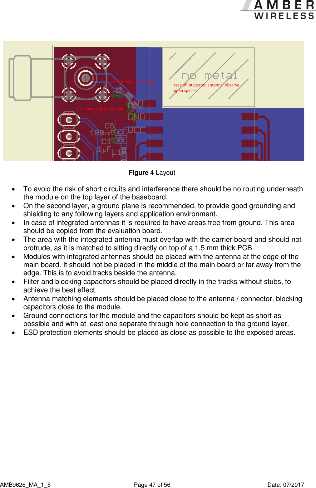
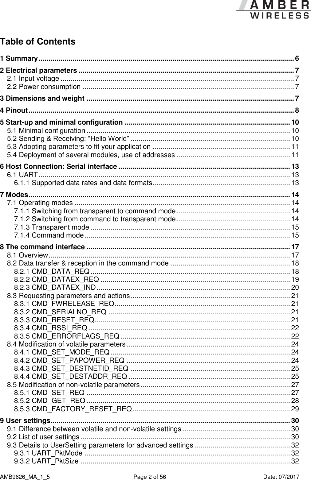
![AMB9626_MA_1_5 Page 51 of 56 Date: 07/2017 To ensure the mechanical stability of the modules it is recommended to solder all the pads of the module to the base board, even if they are not used for the application. Caution! ESD sensitive device. Precaution should be taken when handling the device in order to prevent permanent damage. MSL 3 Caution! This assembly contains moisture sensitive components. Precaution should be taken when processing the device according to IPC/JEDEC J-STD-033. Since the module itself is not fused the voltage supply shall be coming from a limited power source according to clause 2.5 of EN 60950-1. 19 References [1] „CC1125 Single-Chip Low Cost Low Power RF-Transceiver”, Texas Instruments [2] „AMB9626 Datasheet”, AMBER wireless GmbH [3] „Application Report: Asynchronous Channel Hopping System for FCC 15.247 Compliance”, Texas Instruments](https://usermanual.wiki/Wuerth-Elektronik-eiSos-and-Co-KG/AMB9626/User-Guide-3606734-Page-52.png)