XYZprinting NFC001 NFC Module User Manual
XYZprinting, Inc. NFC Module
Users Manual

NFCModule
XYZ‐NFC‐001DataSheet

Features
I2C interface.
I2C-bus interface up to 400 kBd in Fast mode, up to 3400 kBd in High-speed mode
FIFO buffer handles 64 byte send and receive
Flexible interrupt modes
Hard reset with low power function
Power-down mode per software
Programmable timer
Internal oscillator for connection to 27.12 MHz quartz crystal
2.5 V to 5.5 V power supply
CRC coprocessor
Programmable I/O pins
Internal self-test
Pin description
PinSymbolTypeDescription
1VCC_INPWRDigitalPowerSupply
2GNDPWRDigitalGround
3NRSTPDINotResetandPowerDown
4IRQOInterruptRequest
5I2C_SDAI/OI2Cdata
6I2C_SCLII2Caddress
Electrical Characteristics
SymbolParameterMinTypMaxUnit
VDDdigital supply voltage2.5 5.5V
IDDdigital supply current400mA
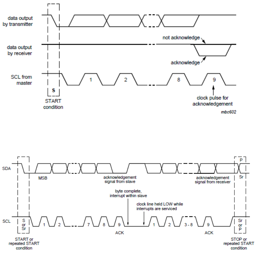
Acknowledge
An acknowledge must be sent at the end of one data byte. The acknowledge-related clock
pulse is generated by the master. The transmitter of data, either master or slave, releases
the SDA line (HIGH) during the acknowledge clock pulse. The receiver pulls down the
SDA line during the acknowledge clock pulse so that it remains stable LOW during the
HIGH period of this clock pulse.
The master can then generate either a STOP (P) condition to stop the transfer or a
repeated START (Sr) condition to start a new transfer.
A master-receiver indicates the end of data to the slave-transmitter by not generating an
acknowledge on the last byte that was clocked out by the slave. The slave-transmitter
releases the data line to allow the master to generate a STOP (P) or repeated START (Sr)
condition.
Acknowledge on the I2C-bus
Data transfer on the I2C-bus
Register read access
To read out data from a specific register address in the Module, the host controller must
use the following procedure:
• Firstly, a write access to the specific register address must be performed as indicated
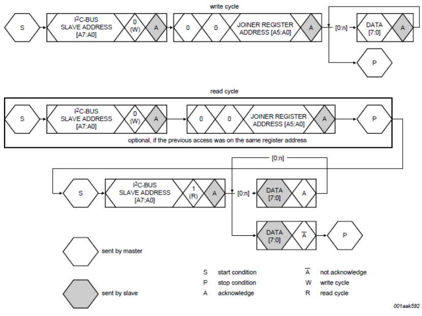
in the frame that follows
• The first byte of a frame indicates the device address according to the I2C-bus rules
• The second byte indicates the register address. No data bytes are added
• The Read/Write bit is 0
After the write access, read access can start. The host sends the device address of the
PN512. In response, the Module sends the content of the read access register. In one
frame all data bytes can be read from the same register address. This enables fast FIFO
buffer access or register polling.
The Read/Write (R/W) bit is set to logic 1.
Register read and write access
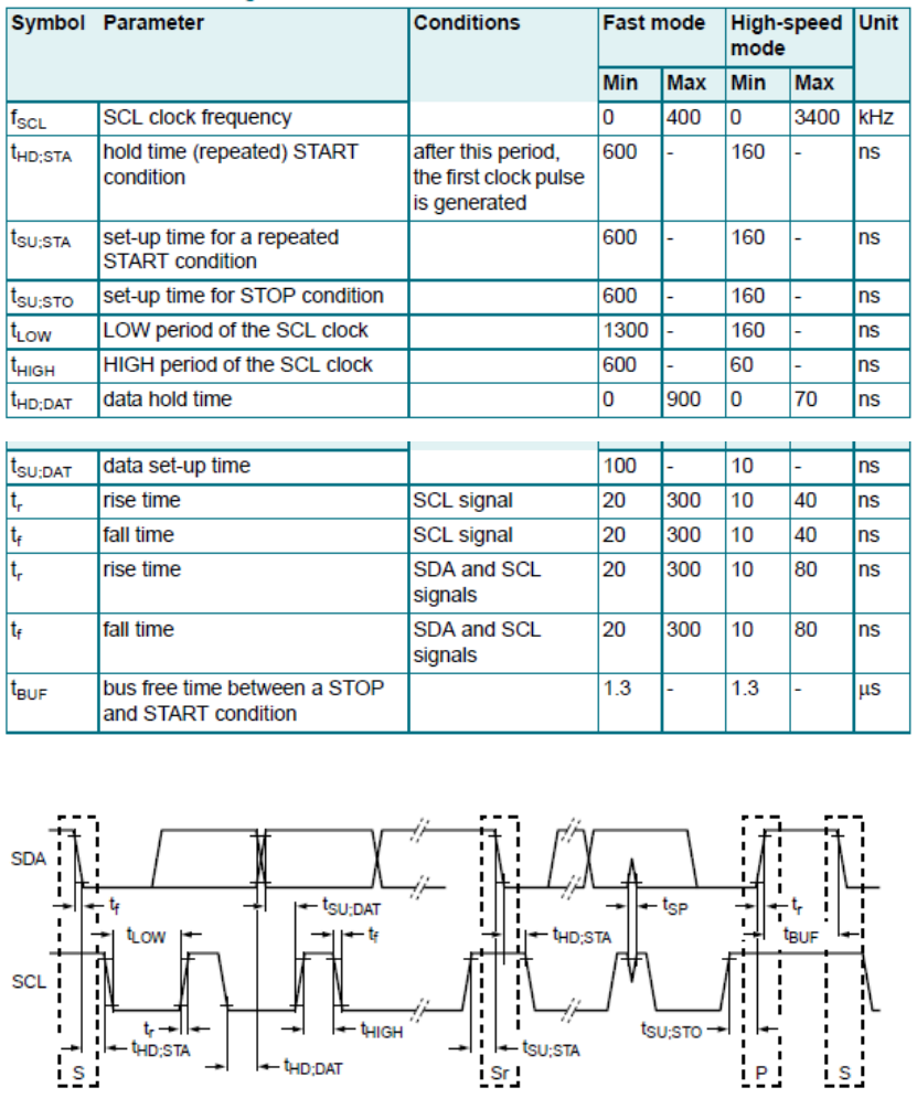
I2C-bus timing
FederalCommunicationCommissionInterferenceStatement
ThisequipmenthasbeentestedandfoundtocomplywiththelimitsforaClassBdigitaldevice,pursuantto
Part15oftheFCCRules.Theselimitsaredesignedtoprovidereasonableprotectionagainstharmful
interferenceinaresidentialinstallation.Thisequipmentgenerates,usesandcanradiateradiofrequency
energyand,ifnotinstalledandusedinaccordancewiththeinstructions,maycauseharmfulinterferenceto
radiocommunications.However,thereisnoguaranteethatinterferencewillnotoccurinaparticular
installation.Ifthisequipmentdoescauseharmfulinterferencetoradioortelevisionreception,whichcan
bedeterminedbyturningtheequipmentoffandon,theuserisencouragedtotrytocorrectthe
interferencebyoneofthefollowingmeasures:
‐Reorientorrelocatethereceivingantenna.
‐Increasetheseparationbetweentheequipmentandreceiver.
‐Connecttheequipmentintoanoutletonacircuitdifferentfromthattowhichthereceiverisconnected.
‐Consultthedealeroranexperiencedradio/TVtechnicianforhelp.
FCCCaution:
Anychangesormodificationsnotexpresslyapprovedbythepartyresponsibleforcompliancecouldvoid
theuser'sauthoritytooperatethisequipment.
ThisdevicecomplieswithPart15oftheFCCRules.Operationissubjecttothefollowingtwoconditions:
(1)Thisdevicemaynotcauseharmfulinterference,and
(2)Thisdevicemustacceptanyinterferencereceived,includinginterferencethatmaycauseundesired
operation.
FCCRadiationExposureStatement:
ThisequipmentcomplieswithFCCradiationexposurelimitssetforthforanuncontrolledenvironment.This
transmittermodulemustnotbeco‐locatedoroperatinginconjunctionwithanyotherantennaor
transmitter.
IMPORTANTNOTE:
Intheeventthattheseconditionscannotbemet(forexamplecertainlaptopconfigurationsorco‐location
withanothertransmitter),thentheFCCauthorizationisnolongerconsideredvalidandtheFCCIDcannot
beusedonthefinalproduct.Inthesecircumstances,theOEMintegratorwillberesponsiblefor
re‐evaluatingtheendproduct(includingthetransmitter)andobtainingaseparateFCCauthorization.
EndProductLabeling:
Thefinalendproductmustbelabeledinavisibleareawiththefollowing:
【ContainsFCCID:2AB9W‐NFC001】
ManualInformationtotheEndUser
TheOEMintegratorhastobeawarenottoprovideinformationtotheenduserregardinghowtoinstallor
removethisRFmoduleintheuser’smanualoftheendproductwhichintegratesthismodule.