Xplore Technologies MC7750 CELLULAR/PCS GSM/EDGE/WCDMA/CDMA+ 700 MHz LTE MODEM User Manual
Xplore Technologies CELLULAR/PCS GSM/EDGE/WCDMA/CDMA+ 700 MHz LTE MODEM
UserManual.wiki
>
Xplore Technologies
>
MC7750 User Manual
User Manual
Navigation menu
Upload a User Manual
Namespaces
Wiki Guide
HTML
PDF
Info
Views
User Manual
Discussion / Help
Navigation

![Rev 4 Sep.11 Proprietary and Confidential - Contents subject to change 1511: IntroductionThe Sierra Wireless MC7750 PCI Express Mini Card is a compact, lightweight, wireless LTE - and CDMA-based modem, designed to be Verizon Wireless certified.The MC7750 provides LTE, CDMA, and GPS connectivity for portable and handheld computers, point-of-sale devices, telemetry products and other machine-to-machine and vertical applications over several radio frequency bands.Supported RF bandsThe modem, based on Qualcomm's MDM9600 baseband processor, supports data operation on LTE and CDMA networks.Physical features•Small form factor—conforms to F1 as specified in PCI Express Mini Card Electromechanical Specification Revision 1.2.•Operating temperature range: -30 °C to +60 °CApplication interface features•USB interface (QMI )•NDIS NIC interface support for Windows 7, Windows Vista, and Windows XP platforms•Multiple non-multiplexed USB channel support•USB selective suspend to maximize power savings•AT command interface ([1] AT Command Set for User Equipment (UE) (Release 6) (Doc# 3GPP TS 27.007), plus proprietary extended AT commands)•Software Development Kit (SDK) including a Linux API (Appli-cation Program Interface)Table 1-1: Supported RF bands Technology Bands DiversityLTE •Band 13: 700 MHz (MIMO)CDMA •Cellular (800 MHz)•PCS (1900 MHz) GPS •1575.42 MHz n/a](https://usermanual.wiki/Xplore-Technologies/MC7750/User-Guide-2026664-Page-15.png)
![IntroductionRev 4 Sep.11 Proprietary and Confidential - Contents subject to change 17•Mobile-originated SMS over IMS for LTE / eHRPDPosition location (GPS)•Standalone mode•GLONASS support on GPS connector 1 (future release)•DC bias on GPS connector 1 to support external active GPS antennaWarranty and supportThe MC7750 offers the following support features:•Standard 1-year warranty•Enabling software (drivers, SDK, etc.) for Android, Linux, Windows 7, Windows Vista, and Windows XPSupporting documentsSeveral additional documents describe Mini Card design, usage, integration, and other features. See References on page 87.AccessoriesThe Universal Development Kit (UDK) is a hardware development platform for AirPrime MC-series modules. It contains hardware components for evaluating and developing with the module, including:•Development board•Cables•Antennas (Bands 17, 13, and 7 are not supported by supplied antennas)•Documentation suite•Initial allotment of support hours•Other accessoriesFor instructions on setting up the UDK, see [4] PCI Express Mini Card Dev Kit Quick Start Guide (Doc# 2130705).For over-the-air LTE testing, ensure that suitable antennas are used. (Two antennas are required for this testing; Sierra Wireless offers an LTE-capable antenna covering 700–2600 MHz BW — please order part number 6000492 (Qty 1 — this contains two antennas).)](https://usermanual.wiki/Xplore-Technologies/MC7750/User-Guide-2026664-Page-17.png)

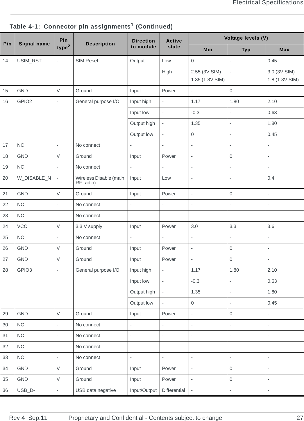
![Electrical SpecificationsRev 4 Sep.11 Proprietary and Confidential - Contents subject to change 29Power supplyThe host provides power to the MC7750 through multiple power and ground pins as summarized in Ta bl e 4-2.The host must provide safe and continuous power at all times; the module does not have an independent power supply, or protection circuits to guard against electrical issues.USB interfaceThe USB interface is the path for communication between the host and module.The interface complies with the [12] Universal Serial Bus Specification, Rev 2.0, and the host device must be designed to the same standard. (When designing the host device, careful PCB layout practices must be followed.)USB interface features include:•Data rate: Full-speed (12 Mbps) / High-speed (480 Mbps)•Module enumeration:·Windows: Modem or COM ports, using host Windows drivers·Linux: / dev / ttyUSBn devices for Linux systems with the Sierra Wireless driver installed•USB-compliant transceivers•Selective suspend mode•Resumption initiated by host or moduleUSB high / full speed throughput performanceThis device has been designed to achieve optimal performance and maximum throughput using USB high speed mode. Although the device may operate with a full speed host, throughput performance will be on an “as is” basis and needs to Table 4-2: Power and ground specifications Name Pins Specification Min Typ Max UnitsVCC 2, 24, 39, 41, 52 Voltage range See Table 4-1 on page 26.Ripple voltage --100 mVppGND 4, 9, 15, 18, 21, 26, 27, 29, 34, 35, 37, 40, 43, 50- - 0 - VTable 4-3: USB interface Name Pin DescriptionUSB_D- 36 USB data negativeUSB_D+ 38 USB data positive](https://usermanual.wiki/Xplore-Technologies/MC7750/User-Guide-2026664-Page-29.png)
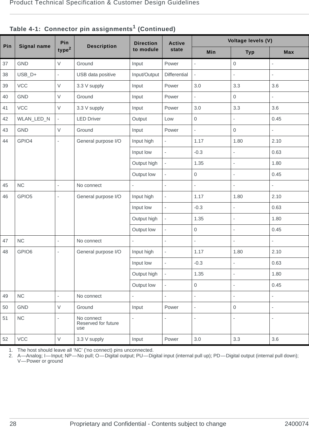
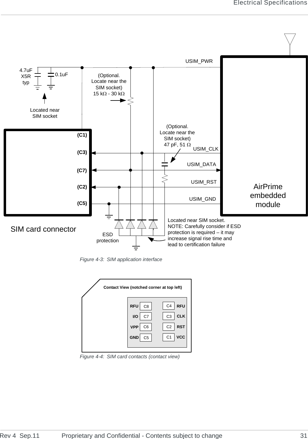
![Product Technical Specification & Customer Design Guidelines30 Proprietary and Confidential - Contents subject to change 2400074be characterized by the OEM. Note that throughput will be reduced and may vary significantly based on packet size, host interface, and firmware revision. Sierra Wireless does not recommend using this device in USB full speed mode.User-developed driversIf you will be developing your own USB drivers, see [5] AirCard / AirPrime USB Driver Developer’s Guide (Doc# 2130634). SIM interfaceThe module supports one SIM (Subscriber Identity Module) (1.8 V or 3 V). The SIM holds account information, allowing users to use their account on multiple devices.The SIM pins (Ta b l e 4-4) provide the connections necessary to interface to a SIM socket located on the host device as shown in Figure 4-3 on page 31. Voltage levels over this interface comply with 3GPP standards. Table 4-4: SIM interface signal Name Pin Description SIM contact number1NotesUSIM_PWR 8SIM voltage 1Power supply for SIMUSIM_DATA 10 Data I/O 7Bi-directional SIM data lineUSIM_CLK 12 Serial clock 3Serial clock for SIM dataUSIM_RST 14 Reset 2Active low SIM resetUSIM_GND Ground 5Ground referenceUSIM_GND is common to module ground1. See Figure 4-4 on page 31 for SIM card contacts.](https://usermanual.wiki/Xplore-Technologies/MC7750/User-Guide-2026664-Page-30.png)
![Electrical SpecificationsRev 4 Sep.11 Proprietary and Confidential - Contents subject to change 33Control interface (Signals)The MC7750 provides signals for:•Power control of the module from the host•LED driver outputThese signals are summarized in Ta b l e 4-5 and paragraphs that follow.W_DISABLE_N — Wireless disableThe host device uses W_DISABLE_N (pin 20) to enable / disable the WWAN or radio modem. When disabled, the modem cannot transmit or receive information.Letting this signal float high allows the module to operate normally. This switch follows the behavior described in [11] PCI Express Mini Card Electromechanical Specification Revision 1.2. This pin has a 20 k pull-up resistor. See Figure 4-5 on page 33 for a recommended implementation.When integrating with your host device, keep the following in mind:•The signal is an input to the module and should be driven LOW only for its active state (controlling the power state); otherwise it should be floating or (High impedance). It should never be driven to a logic high level. The module has an internal pull-up resistor to Module Power (3.3V) in place, so if the signal is floating or (high impedance), the module will power on.•Wait for two seconds after asserting W_DISABLE_N before disconnecting power.•If the host never needs to assert this power state control to the module, leave this signal unconnected from the host interface.Figure 4-5: Recommended wireless disable connectionTable 4-5: Module control signals Name Pin Description Type11. O — Digital pin Output; PU — Digital pin Input, internal pull upW_DISABLE_N 20 Wireless disable (Main RF) PUWLAN_LED_N 42 LED driver OMiniCardRWireless disable control 123Q20kHost3.3V PMIC for W_DISABLE_N](https://usermanual.wiki/Xplore-Technologies/MC7750/User-Guide-2026664-Page-33.png)
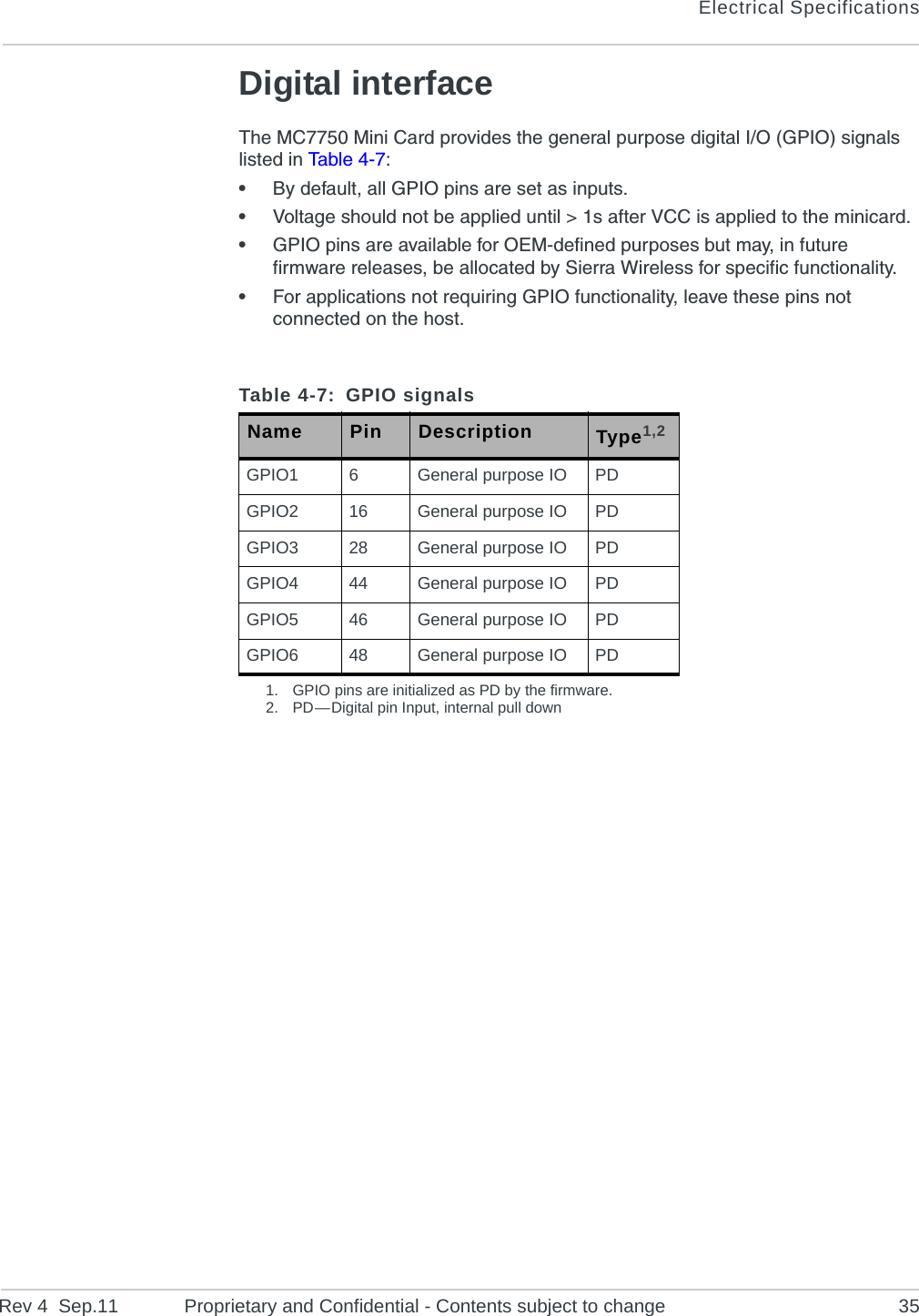
![Product Technical Specification & Customer Design Guidelines34 Proprietary and Confidential - Contents subject to change 2400074WLAN_LED_N — LED outputThe module drives the LED output according to [11] PCI Express Mini Card Electromechanical Specification Revision 1.2, as described in Tab le 4-6 (below).If desired, LED behavior can be configured using AT!LEDCTRL. Figure 4-6: Example LEDTable 4-6: LED states (Default behavior)StateLED behaviorDescription !LEDCTRL indexPeriod (s) On OffOff 00% 100% Module is not powered.(W_DISABLE_N asserted with PCOFFEN=1) N/AAirplane mode 250% 50% Module is in low power mode.(W_DISABLE_N asserted with PCOFFEN=0) 4Power up 5.2 96% 4% Module is performing initial power up activities. N/ASearching 96% 4% Module is searching service. 1Connected 0.5 80% 20% Module has an active context. 3Connected, with data transfer occuring 0.5 80% 20% Module has an active context and data is being transferred. 5Error 1.6 20% 80% Device error has occurred. N/AAttached 1 100% 0% Module has attached to a network and is not currently in a call. 2Current limiting ResistorLEDVCC 3.3VMIOMiniCard](https://usermanual.wiki/Xplore-Technologies/MC7750/User-Guide-2026664-Page-34.png)

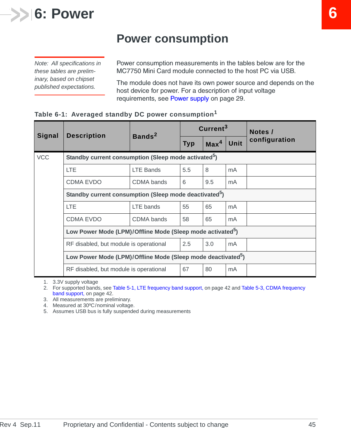
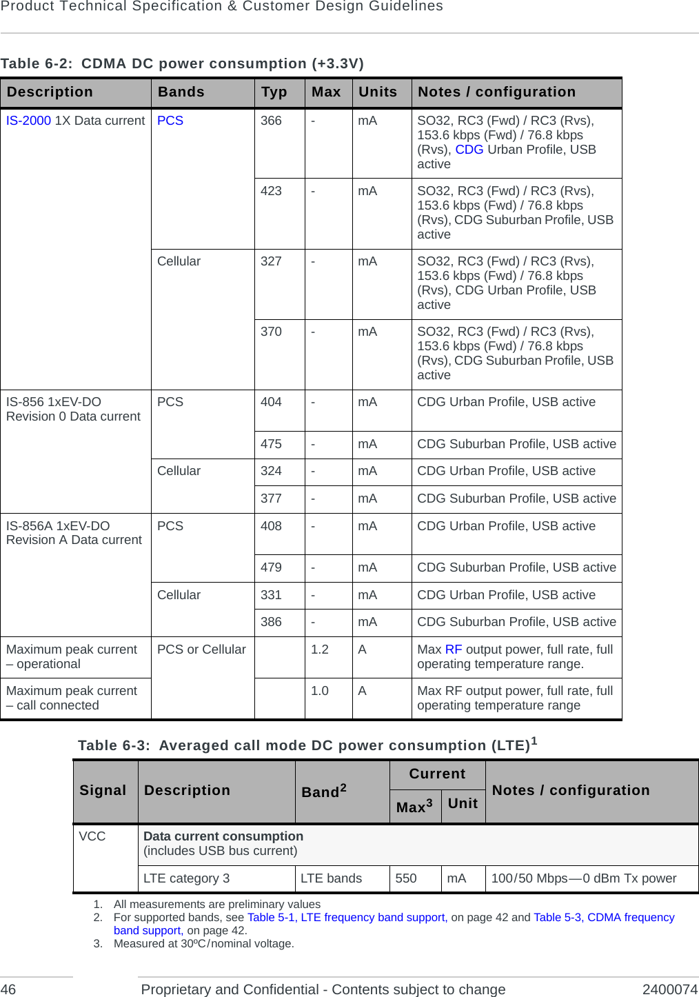
![PowerRev 4 Sep.11 Proprietary and Confidential - Contents subject to change 47Module power statesThe module has five power states, as described in Ta b l e 6-5. Table 6-4: Miscellaneous DC power consumption1 Signal Description Current Unit Notes / configurationTyp MaxVCCModule OFF leakage current 490 830 AFull operating temperature rangeUSB active current 18 25 mA High speed USB connection, CL = 50 pF on D+ and D- signalsInrush current 750 3000 mA•Assumes power supply turn on time > 100µs•Dependent on host power supply rise time.GPS signal connector Active bias on GPS port 3.3 (100 mA) VGPS connector 1 in Figure 5-1 on page 37.1. All measurements are preliminary valuesTable 6-5: Module power states State DetailsHost is poweredModule is poweredUSB interface activeRF enabledNormal(Default state)•Module is active•Default state when VCC is first applied in the absence of W_DISABLE_N control•Module is capable of placing / receiving calls, or establishing data connections on the wireless network•Current consumption is affected by several factors, including:•Radio band being used•Transmit power•Receive gain settings•Data rate•Number of active Tx time slots Low power(‘Airplane mode’)•Module is active•State is controlled by host interface using software commands:•+CFUN=0 ([1] AT Command Set for User Equipment (UE) (Release 6) (Doc# 3GPP TS 27.007))) Sleep •Normal state of module between calls or data connections•Module cycles between wake (polling the network) and sleep, at network provider-determined interval. ](https://usermanual.wiki/Xplore-Technologies/MC7750/User-Guide-2026664-Page-47.png)
![Product Technical Specification & Customer Design Guidelines48 Proprietary and Confidential - Contents subject to change 2400074Power state transitionsThe module uses state machines to monitor supply voltage and operating temperature, and notifies the host when critical threshold limits are exceeded. (See Tabl e 6-6 for trigger details and Figure 6-1 for state machine behavior.)Power state transitions may occur:•Automatically, when critical supply voltage or module temperature trigger levels are encountered.•Under host control, using available AT commands in response to user choices (for example, opting to switch to airplane mode) or operating conditions.Off •Host keeps module powered off by driving W_DISABLE_N low•Module draws minimal current•See W_DISABLE_N — Wireless disable on page 33 for more information.] Disconnected •Host power source is disconnected from the module and all voltages associated with the module are at 0 V. Table 6-5: Module power states (Continued)State DetailsHost is poweredModule is poweredUSB interface activeRF enabledTable 6-6: Power state transitions (including voltage / temperature trigger levels)Transition Voltage Temperature1Notes Trigger V2Trigger °CNormal to Low Power VOLT_HI_CRIT 3.6 TEMP_LO_CRIT -25 •RF activity suspendedVOLT_LO_CRIT 2.9 TEMP_HI_CRIT 95Low Power to Normal VOLT_HI_NORM 3.5 TEMP_NORM_LO -15•RF activity resumedLow Power to NormalorRemain in Normal (Remove warnings)VOLT_LO_NORM 3.1 TEMP_HI_NORM 80Normal (Issue warning) VOLT_LO_WARN 3.0 TEMP_HI_WARN 85Power off / on(Host-initiated) ----•Power off recommended when supply voltage or module operating temperature is critically low or high.1. Module-reported temperatures at the printed circuit board.2. Supply voltage — 3.3V](https://usermanual.wiki/Xplore-Technologies/MC7750/User-Guide-2026664-Page-48.png)

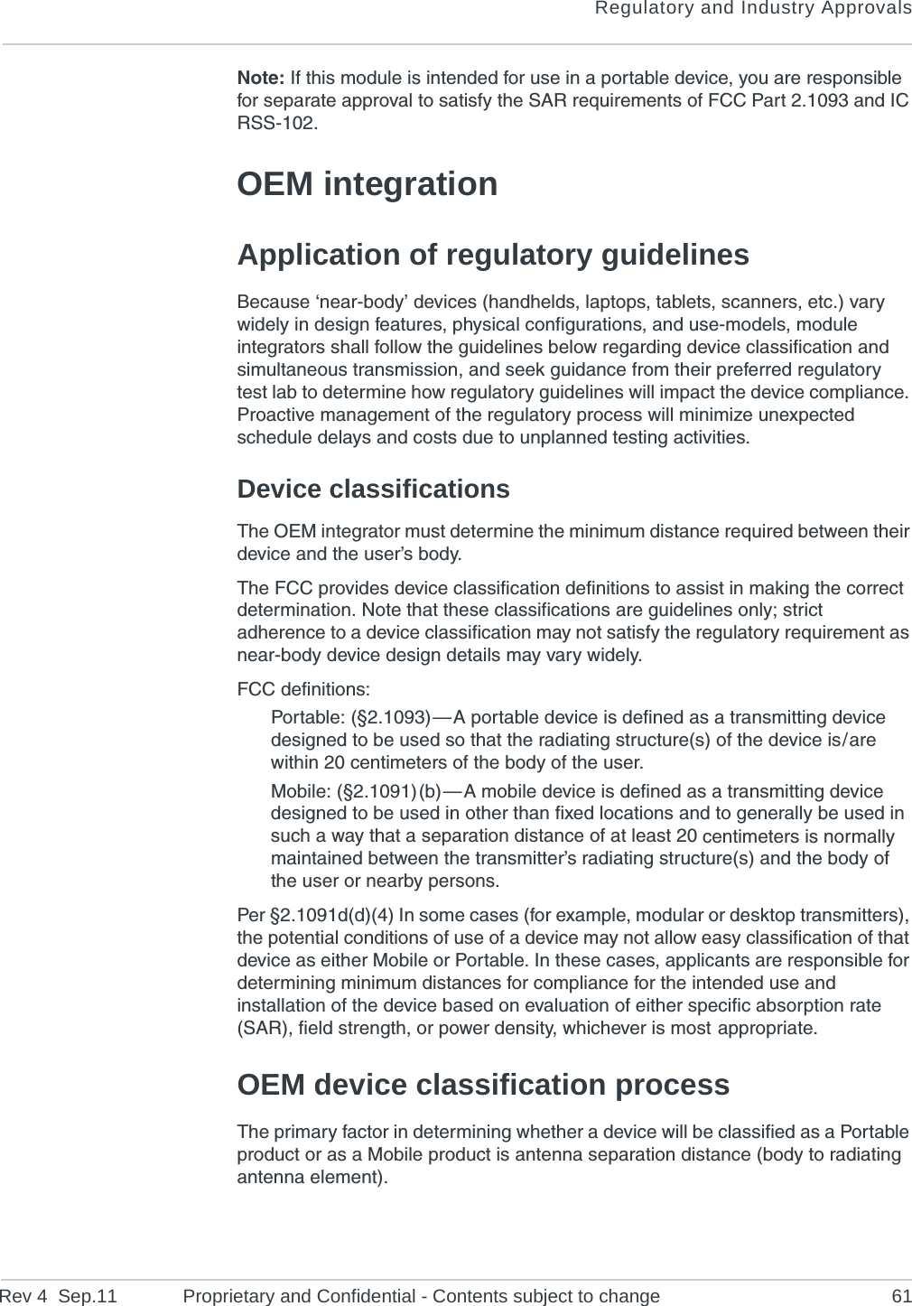
![Product Technical Specification & Customer Design Guidelines56 Proprietary and Confidential - Contents subject to change 2400074Thermal considerationsEmbedded modules can generate significant amounts of heat that must be dissipated in the host device for safety and performance reasons.Figure 8-4: Shield locationsThe amount of thermal dissipation required depends on:•Supply voltage — See Chapter 6: Power on page 45 for details of max power dissipation for various operating modes.•Usage — Typical power dissipation values depend on the location within the host, amount of data transferred, etc.Specific areas requiring heat dissipation are shown in Figure 8-4:•Transmitter — Top face of module near RF connectors. Likely to be the hottest area.•Baseband 1 —Top face of module, below the transmitter.•Receiver — Bottom face of module, behind the transmitter.•Baseband 2 — Bottom face of module, behind Baseband 1.To enhance heat dissipation:•Maximize airflow over / around the module.•Locate the module away from other hot components.•If possible, use the mounting holes to attach (ground) the device to the main PCB ground or a metal chassis.Note: Adequate dissipation of heat is necessary to ensure that the module functions properly, and to comply with the thermal requirements in [11] PCI Express Mini Card Electromechanical Specification Revision 1.2.Caution: Thermal putty is not recommended — incorrect application of the material could require exessive pressure to be applied when seating the board, resulting in damage to the board.TransmitterBaseband 1 Baseband 2ReceiverTop Bottom Pin 1Pin 1](https://usermanual.wiki/Xplore-Technologies/MC7750/User-Guide-2026664-Page-56.png)


![Product Technical Specification & Customer Design Guidelines70 Proprietary and Confidential - Contents subject to change 2400074Provide ESD protection for the SIM connector at the exposed contact point (in particular, the CLK, VCC, IO, and RESET lines).SIM implementation on page 32Keep very low capacitance traces on the USIM_DATA and USIM_CLK signals.SIM implementation on page 32To minimize noise leakage, establish a very good ground connection between the module and host.Ground connection on page 39Route cables away from noise sources (for example, power supplies, LCD assemblies, etc.).Methods to mitigate decreased Rx performance on page 40Shield high RF-emitting components of the host device (for example, main processor, parallel bus, etc.).Methods to mitigate decreased Rx performance on page 40Use discrete filtering on low frequency lines to filter out unwanted high-order harmonic energy.Methods to mitigate decreased Rx performance on page 40Use multi-layer PCBs to form shielding layers around high-speed clock traces.Methods to mitigate decreased Rx performance on page 40ThermalTest to worst case operating conditions — temperature, voltage, and operation mode (transmitter on 100% duty cycle, maximum power).Thermal considerations on page 56Use appropriate techniques to reduce module temperatures (for example, airflow, heat sinks, heat-relief tape, module placement, etc.).Thermal considerations on page 56Host / Modem communicationMake sure the host USB driver supports remote wakeup, resume, and suspend operations, and serial port emulation.[5] AirCard / AirPrime USB Driver Developer’s Guide (Doc# 2130634)When no valid data is being sent, do not send SOF tokens from the host (causes unnecessary power consumption).[5] AirCard / AirPrime USB Driver Developer’s Guide (Doc# 2130634)Table B-1: Hardware integration design considerations (Continued)Suggestion Section where discussed](https://usermanual.wiki/Xplore-Technologies/MC7750/User-Guide-2026664-Page-70.png)
![Product Technical Specification & Customer Design Guidelines74 Proprietary and Confidential - Contents subject to change 2400074Suggested production testsConsider the following tests when you design your production test procedures for devices with the AirPrime module installed.•Visual check of the module’s connectors and RF assemblies•Module is operational•USB connection is functional•LED is functional•W_DISABLE_N (module power down)•Firmware revision check•Rx tests on main and auxiliary paths•Tx testProduction test procedureThe following is a suggested test plan — you must decide which tests are appropriate for your product. You may wish to add additional tests that more fully exercise the capabilities of your product.Using an appropriate Dev Kit-based test station, and referring to the appropriate AT command references:1. Visually inspect the module’s connectors and RF assemblies for obvious defects before installing it in the test station.2. Ensure that the module is turned off before beginning your tests — Drive W_DISABLE_N low.3. If using Linux, determine if any USB devices are currently connected to the computer:a. Open a shell window and enter the command ls / dev / tty / USB*.b. Record the ttyUSBn values that are returned; these are the currently connected USB devices. If the command returns “no such file or directory”, there are no devices currently connected.4. Tes t W_DISABLE_N — Turn on the module by letting W_DISABLE_N float (high impedance).5. Test USB functionality — Check for USB enumeration.·(Windows systems) The Device Manager shows Sierra Wireless items under Ports (COM & LPT). The devices shown depend on the module type. For example:]·(Linux systems) Enter the command ls / dev / tty / USB* and then record and compare the results with those from Step 3. If there are any new ttyUSBn devices, then the modem has enumerated successfully. (There should be seven new devices) For example:](https://usermanual.wiki/Xplore-Technologies/MC7750/User-Guide-2026664-Page-74.png)
![TestingRev 4 Sep.11 Proprietary and Confidential - Contents subject to change 81•Power consumption•Originate and terminate data and voice (if applicable) calls•Cell hand-off•Transmitter and receiver tests•FER (Frame Error Rate) as an indicator of receiver sensitivity / performance•Channel and average power measurements to verify that the device is trans-mitting within product specifications•RF sensitivity tests•CDMA:·FER testing — Test receiver sensitivity for conditions of minimum cell power. FER can be measured for the specified receiver sensitivity of -104 dBm. The objective of this test is to determine if the FER measured is within the acceptable limits for the specified receiver sensitivity of the module. Unlike the FER tests performed during production testing, this test determines the receiver performance without the influence of the noise factor (AWGN), but with extremely low cell power. The reported FER and the confidence level must be <1% and >95% respectively for the test to be considered a pass.Suggested testing equipmentTo perform production and post-production tests, you will require appropriate testing equipment. A test computer can be used to coordinate testing between the integrated module (on the development kit or host) and the measurement equipment, usually with GPIB connections. The suggested setup includes a power meter to test RF output power and a signal generator to evaluate the receiver.Testing assistance provided by Sierra WirelessExtended AT commands have been implemented to assist with performing FTA GCF tests and portions of CE Mark tests requiring radio module access. These are documented in the [2] AirCard / AirPrime UMTS Devices Supported AT Command Reference (Doc# 2130617) and [3] AirPrime MC8xxx Embedded Modules Extended AT Command Reference (Doc# 2130616).Sierra Wireless offers optional professional services based assistance to OEMs with regulatory approvals.IOT/Operator testingInteroperability and Operator/Carrier testing of the finished system is the responsibility of the OEM. The test process will be determined with the chosen network operator(s) and will be dependent upon your business relationship with them, as well as the product's application and sales channel strategy.Sierra Wireless offers assistance to OEMs with the testing process, if required.](https://usermanual.wiki/Xplore-Technologies/MC7750/User-Guide-2026664-Page-81.png)
![Product Technical Specification & Customer Design Guidelines82 Proprietary and Confidential - Contents subject to change 2400074Extended AT commands for testingSierra Wireless provides proprietary AT commands that may help in hardware integration design and testing (these commands are NOT intended for use by end users):•[3] AirPrime MC8xxx Embedded Modules Extended AT Command Reference (Doc# 2130616)•[2] AirCard / AirPrime UMTS Devices Supported AT Command Reference (Doc# 2130617)Some useful commands from these documents for use in hardware integration are listed in Tabl e C-2 on page 82. Table C-2: Extended AT commands Command DescriptionPassword commands!ENTERCND Enable access to password-protected commands!SETCND Set AT command passwordModem reset and status commands!GRESET Reset the modem!GSTATUS Return the operation status of the modem (mode, band, channel, and so on)Diagnostic commands!BAND Select a set of frequency bands or reports current selection!GBAND Read / set the current operating bandTest commands!ALLUP Turn transmitter on / off and simulate ‘All UPs’!CHAN Tune synthesizer to channel / band!DAFTMACT Put the modem into FTM (Factory Test Mode)!DAFTMDEACT Put the modem into online mode!DAGGRSSI Return the RSSI (Received Signal Strength Indicator) in dBm (GSM mode)!DAGGAVGRSSI Return an averaged RSSI (Received Signal Strength Indicator) in dBm (GSM mode)!DAGGRSSIRAW Return the raw RSSI (GSM mode)!DAGINFO Return GSM mode RF information!DAGSLOCK Return the RF synthesizer lock state!DAGSRXBURST Set the GSM receiver to burst mode!DAGSRXCONT Set the GSM receiver continually on](https://usermanual.wiki/Xplore-Technologies/MC7750/User-Guide-2026664-Page-82.png)

![ERev 4 Sep.11 Proprietary and Confidential - Contents subject to change87E: ReferencesThis guide deals specifically with hardware integration issues that are unique to AirPrime embedded modules.Web site supportFor additional documents describing embedded module design, usage, and integration issues (AT command references, integration guides, etc.), visit www.sierrawireless.com/minicard. To obtain access permission, contact your Sierra Wireless account representative.Sierra Wireless documentsThe following Sierra Wireless documents are available from www.sierrawireless.com.Command documents[1] AT Command Set for User Equipment (UE) (Release 6) (Doc# 3GPP TS 27.007)[2] AirCard / AirPrime UMTS Devices Supported AT Command Reference (Doc# 2130617)[3] AirPrime MC8xxx Embedded Modules Extended AT Command Reference (Doc# 2130616)Other Sierra documents[4] PCI Express Mini Card Dev Kit Quick Start Guide (Doc# 2130705)[5] AirCard / AirPrime USB Driver Developer’s Guide (Doc# 2130634)Industry / other documentsThe following non-Sierra Wireless references are not included in your documentation package:[6] CDMA 1x Standard (CDMA 200 Series Release A (2000)) (Doc# TIA/EIA/IS-2000 Series, Release A)[7] FCC Regulations - Part 15 - Radio Frequency Devices[8] IEC-61000-4-2 level 3[9] IEC-61000-4-2 level (Electrostatic Discharge Immunity Test)[10]Mobile Station (MS) Conformance Specification; Part 4: Subscriber Interface Module (Doc# 3GPP TS 11.10-4)](https://usermanual.wiki/Xplore-Technologies/MC7750/User-Guide-2026664-Page-87.png)
![Product Technical Specification & Customer Design Guidelines88 Proprietary and Confidential - Contents subject to change2400074[11] PCI Express Mini Card Electromechanical Specification Revision 1.2[12] Universal Serial Bus Specification, Rev 2.0[13] JESD22-A114-B[14] JESD22-C101](https://usermanual.wiki/Xplore-Technologies/MC7750/User-Guide-2026664-Page-88.png)