Z Com XG182MV02 Wirless Module User Manual USer Manual
Z Com Inc Wirless Module USer Manual
UserManual.wiki
>
Z Com
>
XG182MV02 User Manual
>
USer Manual
Contents
1.
USer Manual
2.
user manual
USer Manual
Navigation menu
Upload a User Manual
Namespaces
Wiki Guide
HTML
PDF
Info
Views
User Manual
Discussion / Help
Navigation
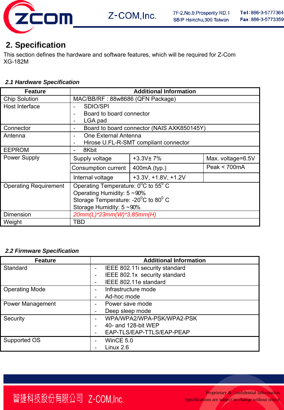
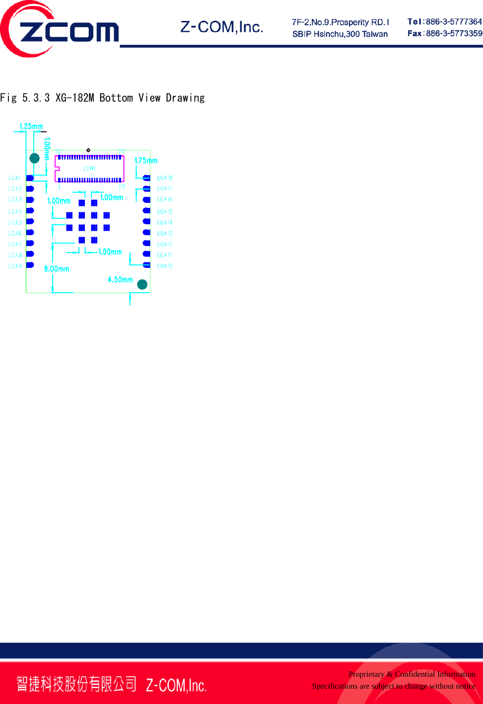
![Proprietary & Confidential InformationSpecifications are subject to change without noticeFIRM Pin.58 2-Wire BCA Mode: When high, WLAN is transmitting or receiving packets. 3-Wire BCA Mode: 0 = Bluetooth device allowed to transmit 1 = Bluetooth device not allowed to transmit This pin drives low when PDn is asserted. In WLAN Sleep mode, all I/O pads are powered down. This pad must stay at a low state even in power down mode. 5 8 BT_PRIORITY I 88W8686 Pin.59 Bluetooth Priority 2-Wire BCA Mode: When high, Bluetooth is transmitting or receiving high priority packets. 3-Wire BCA Mode: When high, Bluetooth is transmitting or receiving packets. 49 9 SDIO_SPI_SEL O 88W8686 Pin.22 or Pin.24 High or NC for SDIO, low for SPI interface 9 13 SPI_SDI/SD_CMD I/O 88W8686 Pin.43 G-SPI Mode: SPI_SDI G-SPIData Input SDIO 4-bit Mode: SD_CMD Command/Response SDIO 1-bit Mode: SD_CMD Command Line SDIO SPI Mode: SD_CMD Data Input 10 12 SPI_SINTn/ SD_D2 I/O 88W8686 Pin.46 G-SPI Mode: SPI_SINTn G-SPI Interrupt Output (active low) SDIO 4-bit Mode: SD_D2 Data Line Bit[2] or Read Wait (optional) SDIO 1-bit Mode: SD_D2 Read Wait (optional) SDIO SPI Mode: SD_D2 Reserved 25 11 SPI_SCSn/SD_D0 I 88W8686 Pin.44 G-SPI Mode: SPI_SCSn G-SPI Chip Select Input (active low) SDIO 4-bit Mode: SD_D0 Data Line Bit [0] SDIO 1-bit Mode: SD_D0 Data Line SDIO SPI Mode: SD_D0 Data Output](https://usermanual.wiki/Z-Com/XG182MV02.USer-Manual/User-Guide-1023570-Page-7.png)
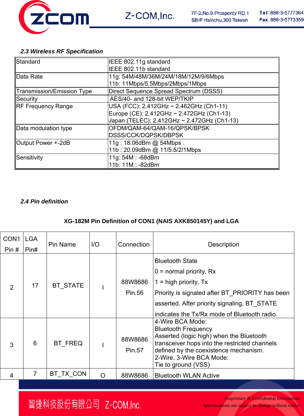
![Proprietary & Confidential InformationSpecifications are subject to change without notice32 16 SPI_CLK/SD_CLK I/O 88W8686 Pin.42 G-SPI Mode: SPI_CLK G-SPI Clock Input SDIO 4-bit Mode: SD_CLK Clock Input SDIO 1-bit Mode: SD_CLK Clock Input SDIO SPI Mode: SD_CLK Clock Input 34 15 SPI_SDO/SD_D1 I/O 88W8686 Pin.45 G-SPI Mode: SPI_SDO G-SPI Data Output SDIO 4-bit Mode: SD_D1 Data Line Bit [1] SDIO 1-bit Mode: SD_D1 Interrupt SDIO SPI Mode: SD_D1 Reserved 35 14 SD_D3 I/O 88W8686 Pin.47 SDIO 4-bit Mode: SD_D3 Data Line Bit [3] SDIO 1-bit Mode: SD_D3 Reserved SDIO SPI Mode: SD_D3 Card Select (active low) 39 5 GPIO0 I/O 88W8686 Pin.11 46 4 GPIO1 I/O 88W8686 Pin.40 Internal pull-up General Purpose Input/Output These pins are asynchronous to internal clocks. Several of these pins can be selected to perform alternate functions such as an LED controller. When not used, these pins should be left floating.GPIO1 – LED output (strap pin) (Tx power or Rx ready LED) GPIO0 – external oscillator control/SLEEPn; Wake up control During power down sleep mode, the external crystal oscillator is disabled, and, if implemented, also powered down by GPIO0 13,38 2,3 3.3V Power ― Power supply from host 1, 50 1,18,10 GND Ground ― Ground 6,7,8,11,12,14,15,16,17,18,19,2NC NC NC NC NC](https://usermanual.wiki/Z-Com/XG182MV02.USer-Manual/User-Guide-1023570-Page-8.png)