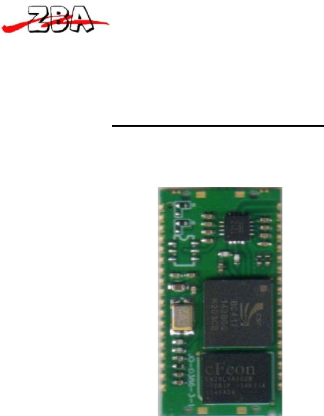
ZBA BT44-111S Class 1 Bluetooth Module User Manual Users manual
ZBA, Inc. Class 1 Bluetooth Module Users manual
ZBA >
Users Manual
ZBA, Inc.
ZBA Bluetooth 2.0 Class 1 Module
Assembly No. BT44 – 111S
ZBA, Inc
94 Old Camplain Road,
Hillsborough, NJ 08844
www.zbausa.com
Page 1

ZBA, Inc.
Table of Contents
1
2
3
4
5
6
7
Document Status .............................................................................................................. 4
Scope................................................................................................................................ 5
Bluetooth Assembly Description ..................................................................................... 5
Features ............................................................................................................................ 5
Applications ..................................................................................................................... 6
Block Diagram ................................................................................................................. 6
Pin-out and Mechanical Specifications............................................................................ 7
7.1
7.2
7.3
Pin Configurations..................................................................................................... 7
Dimensional Drawing ............................................................................................... 9
PCB Land Patterns .................................................................................................. 10
8 General Specifications ................................................................................................... 11
8.1 Electrical Characteristics ......................................................................................... 11
8.1.1
8.1.2
Absolute Maximum Ratings ............................................................................ 11
Input/Output Terminal Characteristics ............................................................ 11
8.2 Radio Characteristics: Basic Data Rate................................................................... 12
8.2.1
8.2.2
8.2.3
Transmitter (Temperature =20oC) .................................................................. 12
Basic Data Rate---Receiver (Temperature =20oC) ......................................... 13
Radio Characteristics: Enhanced Data Rate .................................................... 14
8.2.3.1
8.2.3.2
Transmitter (Temperature = +20°C)......................................................... 14
Receiver (Temperature = +20°C) ............................................................. 16
9 Typical Application Circuit ........................................................................................... 18
10 Serial Port Profile........................................................................................................... 19
10.1
10.2
Default Configuration.......................................................................................... 19
Configuration Commands Set-up & Procedures ................................................. 19
10.2.1 Entering the Set-up Mode ................................................................................ 20
10.2.2 Testing the Communication Link .................................................................... 20
10.2.3 Command list ................................................................................................... 20
10.2.4 Set RS232 Baud Rate (bps).............................................................................. 20
10.2.5 Set/inquired UART Parameters ....................................................................... 21
10.2.6 Set Authentication............................................................................................ 21
10.2.7 Set Password .................................................................................................... 21
10.2.8 Set Device Name.............................................................................................. 21
10.2.9 Set Device Type ............................................................................................... 22
10.2.10
10.2.11
10.2.12
10.2.13
10.2.14
10.2.15
10.2.16
10.2.17
10.2.18
10.2.19
10.2.20
Set Master/Slave Mode ................................................................................ 22
Set Sniff Power Saving Mode ...................................................................... 22
Set Sniff Power Saving Mode—Extended ................................................... 22
Reset to Factory Default............................................................................... 22
Set/Inquire Scan Time .................................................................................. 22
Set/Inquire Paired Device............................................................................. 23
Clear Paired Device Address........................................................................ 23
Inquire Version............................................................................................. 24
Inquire Remote Device Address .................................................................. 24
Set/Inquire Paired Device Address .............................................................. 24
Cancel Inquiry .............................................................................................. 24
Page 2

ZBA, Inc.
10.2.21
10.2.22
10.2.23
10.2.24
10.2.25
10.2.26
Inquire Device BD Address ......................................................................... 25
Software Reset.............................................................................................. 25
Set/Inquire about Low power mode ............................................................. 25
Set/Inquire Data processing mode at BT disconnect ................................... 25
Set/Inquire about Flow control mode (Handshaking) .................................. 25
Exiting the Set-up Mode .............................................................................. 26
11 Low Power Modes ......................................................................................................... 26
11.1 Park & Sniff......................................................................................................... 26
12 Mounting Recommendations ......................................................................................... 27
13 Solder Profiles................................................................................................................ 27
14 Ordering Information ..................................................................................................... 28
List of Figures
Figure 1: Block Diagram of the BT Module............................................................................ 6
Figure 2 Pin Configuration of the BT44-111S Module (top view) ........................................ 7
Figure 3 Dimensional Drawing of the BT44-111S (top & side views) ................................... 9
Figure 4 Dimensional drawing of the recommended PCB footprint .................................... 10
Figure 5 Schematic of typical application circuit ................................................................. 18
Figure 6 Cross-section of recommended mounting of the BT module................................. 27
Disclaimer:
No part of this document may be copied or reproduced in any form or by any means, or transferred to any third
party, without the prior written consent of an authorized representative of ZBA, Inc. (“ZBA”). The information
in this document is subject to change without notice. ZBA assumes no responsibility for any errors or
omissions that may appear in this document, and disclaims responsibility for any consequences resulting from
the use of the information set forth herein. ZBA makes no commitments to update or to keep current
information contained in this document. The products listed in this document are not suitable for use in
applications such as, but not limited to, aircraft control systems, aerospace equipment, submarine cables,
nuclear reactor control systems and life support systems. Moreover, ZBA does not recommend or approve the
use of any of its products in life support devices or systems or in any application where failure could result in
injury or death. If a customer wishes to use ZBA products in applications not intended by ZBA, said customer
must contact an authorized ZBA representative to determine ZBA’s willingness to support a given application.
The information set forth in this document does not convey any license under the copyrights, patent rights,
trademarks or other intellectual property rights claimed and owned by owned by ZBA. The information set
forth in this document is considered to be “Proprietary” and “Confidential” property
ALL PRODUCTS SOLD BY ZBA ARE COVERED BY THE PROVISIONS APPEARING IN ZBA’S
TERMS AND CONDITIONS OF SALE ONLY, INCLUDING THE LIMITATIONS OF LIABILITY,
WARRANTY AND INFRINGEMENT PROVISIONS. ZBA MAKES NO WARRANTIES OF ANY KIND,
EXPRESS, STATUTORY, IMPLIED OR OTHERWISE, REGARDING INFORMATION SET FORTH
HEREIN OR REGARDING THE FREEDOM OF THE DESCRIBED PRODUCTS FROM INTELLECTUAL
PROPERTY INFRINGEMENT, AND EXPRESSLY DISCLAIMS ANY SUCH WARRANTIES
INCLUDING WITHOUT LIMITATION ANY EXPRESS, STATUTORY OR IMPLIED WARRANTIES OF
MERCHANTABILITY OR FITNESS FOR A PARTICULAR PURPOSE.
Page 3
Date Comments
February 2008 http://www.zbausa.com publication
June 2008
November 2008 Updated contact info
Added PNs for additional profiles
February 2012 Update pin orientation drawings
ZBA, Inc.
1 Document Status
To make a request for change, correction, additions or information on references,
please contact:
ZBA, Inc.
94 Old Camplain Road
Hillsborough, NJ 08844
Phone: 908-359-2070
Fax 908-595-0909
E-mail: techsupport@zbausa.com
Website : http://www.zbausa.com
Page 4

ZBA, Inc.
2 Scope
The intention of this specification is to provide general guidelines on the integration
of the BT44-111S Bluetooth assembly. This product, which complies with Bluetooth
Specification 2.0, is designed to help companies offer Bluetooth enabled products by
speeding their development processes with a ready to integrate Bluetooth assembly with
external antenna attachment.
3 Bluetooth Assembly Description
The BT44-111S is a general purpose surface mount Bluetooth module with an 50 ohm
antenna drive. The BT44-111S Bluetooth Module is a Class 1 Bluetooth module using
BlueCore4-External chipset from Cambridge Silicon Radio, a leading Bluetooth chipset
supplier. It provides a fully compliant Bluetooth system for data and voice communications.
The module interfaces with a host via UART (USB optional) and supports EDR data rate up
to 3Mbps modulation modes. The module and device firmware is fully compliant with the
Bluetooth specification V2.0.
The Bluetooth assembly is available in four different variants:
1) UART transport with serial port emulation (Serial Port Profile)
2) UART transport with HCI interface
3) UART transport with HID interface
4) UART transport with OBEX and FTP profiles
Modules with profiles corresponding to variants 2, 3 and 4 are available upon special
request.
4 Features
Operating Frequency Band 2.40 GHz~2.48GHz unlicensed ISM Band
Bluetooth Spec. v2.0 Compliant + Enhanced Data Rate (EDR)
• EDR compliant with v2.0.E.2 of specification for both 2Mbps and 3Mbps
modulation modes
Class 1 Output Power Range up to 100m
Firmware Upgrade Support (via the UART)
Solder down connections
Active Bluetooth Connections signal
Piconet Support, up to 7 Slaves
USB 2.0 and UART Host Interface
PCM Audio Interface
Low Voltage Power Supply, 2.7V to 3.6V
Built-in 8Mbit Flash Memory
Low Power Modes Available: Park, Sniff, Hold and Deep Sleep
Dimensions: 27.5 x 14.5 x 2 mm
Page 5
ZBA, Inc.
5 Applications
PCs, PDAs
Computer Accessories (CF Cards, USB Dongles, PCMCIA, RS232 Adaptors, etc.)
Mice, Keyboards, Joysticks
Cordless Phones
FAX, Printer Adaptors
Digital Cameras
Access Points to LAN and/or Dial-up network
6 Block Diagram
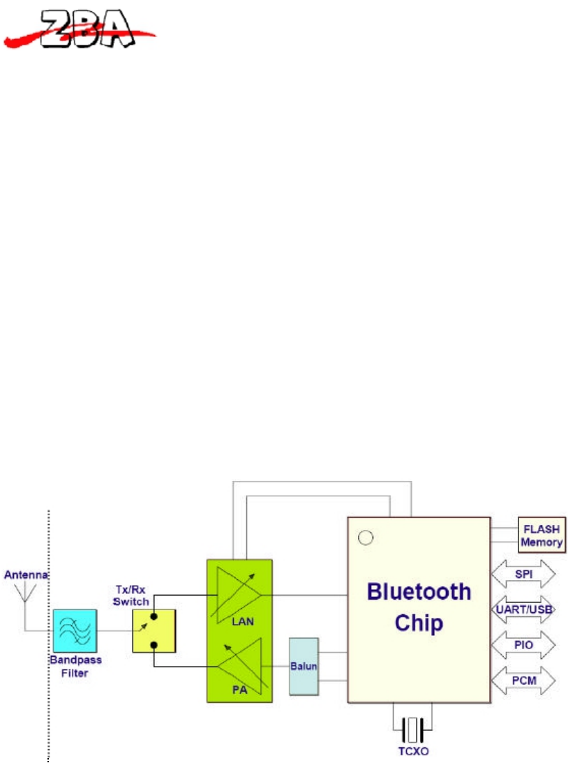
The transmitter design consists of a Bluetooth Chip device connected to an Atmel power
amplifier via a matching network and balun. Harmonic filtering, a transmit/receive switch, a
ceramic bandpass filter and a SMA connector are also included.
The receiver uses the same antenna, bandpass filter and transmit/receive switch as the
transmitter. To improve the sensitivity, the LNA within the Atmel device and the single-
ended receiver port of Bluetooth Chip are used.
Figure 1: Block Diagram of the BT Module
Page 6
Pin # Name Type Description
1 ANT I/O Transmitter out and receiver
input
2 GND GND Ground
3 PIO2 Bi-directional with
programmable strength
internal pull-up/down
Programmable Input/Output Line
4 PIO3 Bi-directional with
programmable strength
internal pull-up/down
Programmable
Input/Output Line
5 PIO[4]/
BT_Priority/
Ch_Clk
Bi-directional with
programmable strength
internal pull-up/down
Programmable input/output line
or Optionally BT_Priority/Ch_Clk
output for co-existence signaling
6 6 PIO[5]/
BT_Active Bi-directional with
programmable strength
internal pull-up/down
Programmable input/output line
or Optionally BT_Active output
for co-existence signaling
ZBA, Inc.
7 Pin-out and Mechanical Specifications
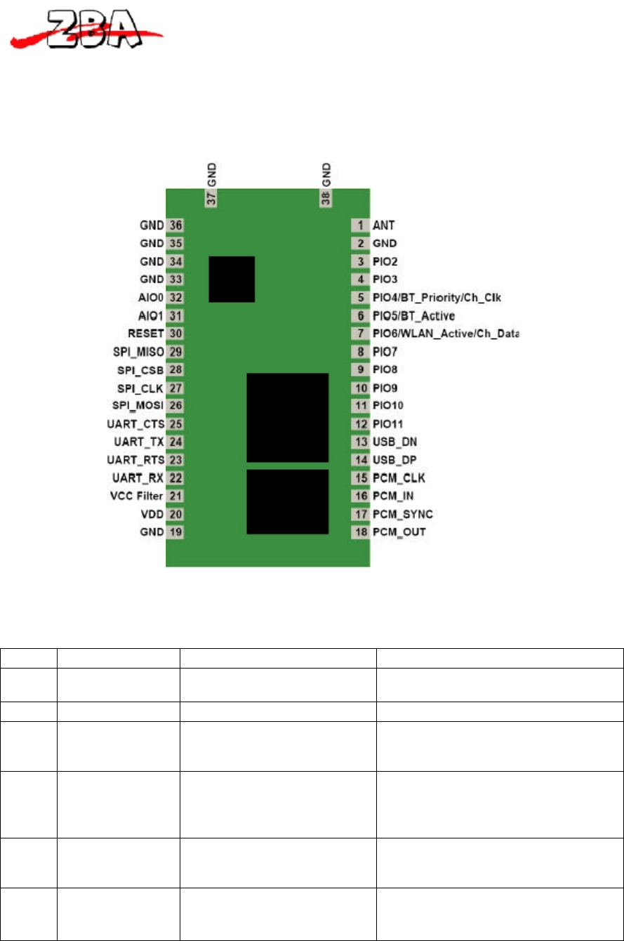
7.1 Pin Configurations
Figure 2 Pin Configuration of the BT44-111S Module (top view)
Page 7

7 PIO[6]/
WLAN_Active/
Ch_Data
Bi-directional with
programmable strength
internal pull-up/down
Programmable input/output line
or Optionally
WLAN_Active/Ch_Data input for
co-existence signaling
8 PIO7 Bi-directional with
programmable strength
internal pull-up/down
Programmable Input/Output Line
9 PIO8 Bi-directional with
programmable strength
internal pull-up/down
Programmable Input/Output Line
10 PIO9 Bi-directional with
programmable strength
internal pull-up/down
Programmable Input/Output Line
11 PIO10 Bi-directional with
programmable strength
internal pull-up/down
Programmable Input/Output Line
12 PIO11 Bi-directional with
programmable strength
internal pull-up/down
Programmable Input/Output Line
13 USB_DN Bi-directional USB Data-
14 USB_DP Bi-directional USB Data+
15 PCM_CLK Bi-directional with weak
internal pull-down Synchronous Data Clock
16 PCM_IN CMOS input, with weak
internal pull-down Synchronous data input
17 PCM_SYNC Bi-directional with weak
internal pull-down Synchronous Data Strobe
18 PCM_OUT CMOS output, tri-state,
with weak internal
pull-down
Synchronous Data Output
19 GND GND Ground
20 VDD Power Supply 3.3 V for RF circuit
221 VCC Filter Filter Capacitor for 1.8V
22 UART_RX CMOS input with weak
internal pull-down Asynchronous Serial Data
23 UART_RTS CMOS output, tri-state,
with weak internal pull-up UART ready to send
24 UART_TX CMOS output, tri-state,
with weak internal pull-up Asynchronous Serial Data
Output
25 UART_CTS CMOS input with weak
internal pull-down UART clear to send
26 SPI_MOSI CMOS input with weak
internal pull-down Synchronous Serial Interface
Data Input
27 SPI_CLK CMOS input with weak
Internal pull-down Synchronous Serial Interface
Clock
28 SPI_CSB CMOS input with weak
internal pull-up Chip select for Synchronous
Serial Interface
29 SPI_MISO CMOS output, tri-state,
with weak internal
pull-down
Synchronous Serial Interface
Data Input
30 RESET CMOS input with weak internal pull-up Reset if low. Input
ZBA, Inc.
Page 8
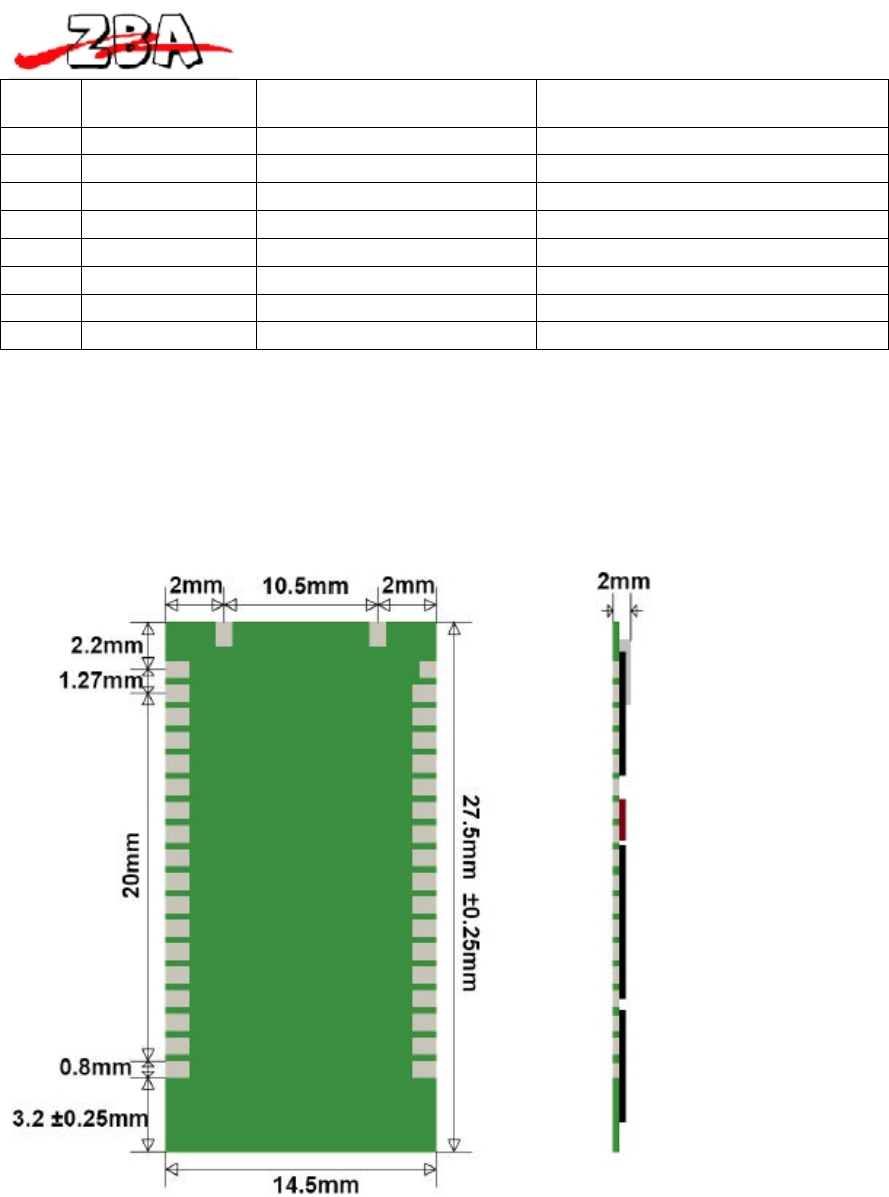
internal pull-up de-bounced so must be low for
>5ms to cause a reset
31 AIO1 Bi-directional Programmable Input/Output line
32 AIO0 Bi-directional Programmable Input/Output line
33 GND GND Ground
34 GND GND Ground
35 GND GND Ground
36 GND GND Ground
37 GND GND Ground
38 GND GND Ground
ZBA, Inc.
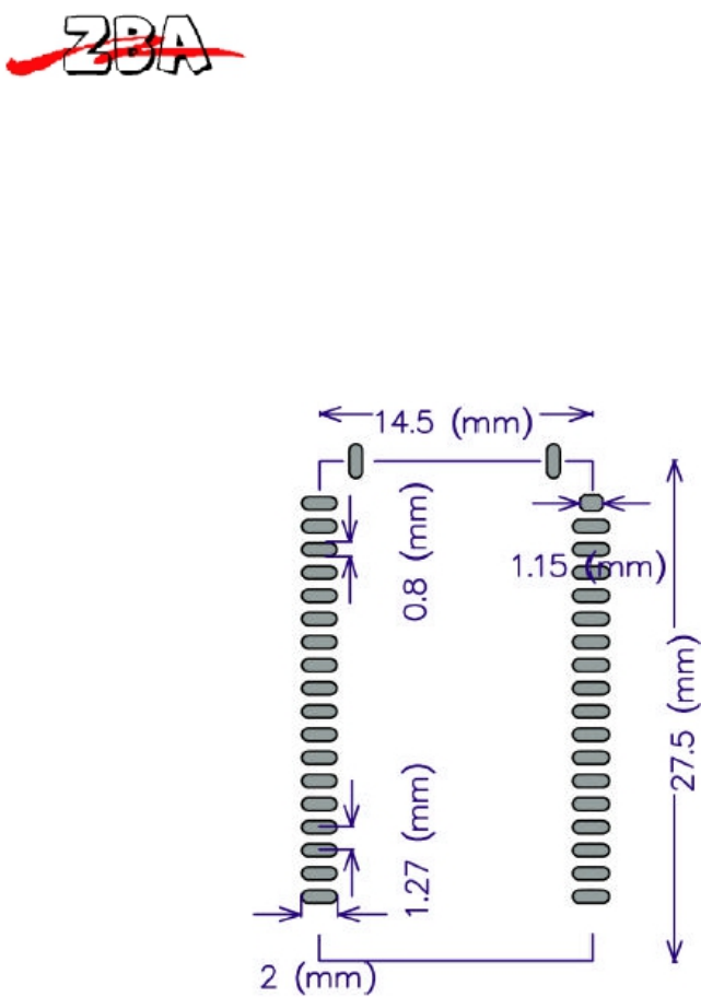
7.2 Dimensional Drawing
Figure 3 Dimensional Drawing of the BT44-111S (top & side views)
Page 9
ZBA, Inc.
7.3 PCB Land Patterns
The BT44-111S is a solder down Bluetooth module. The pad is an edge style pad with a
pitch of 50mils. The exact dimensions of the pad should always be cross-checked with the
manufacturer of the PCB and the assembly locations. The dimensions shown below are only
recommended dimensions and are used on our testing boards. See Figure 4 below.
Figure 4 Dimensional drawing of the recommended PCB footprint
Page 10
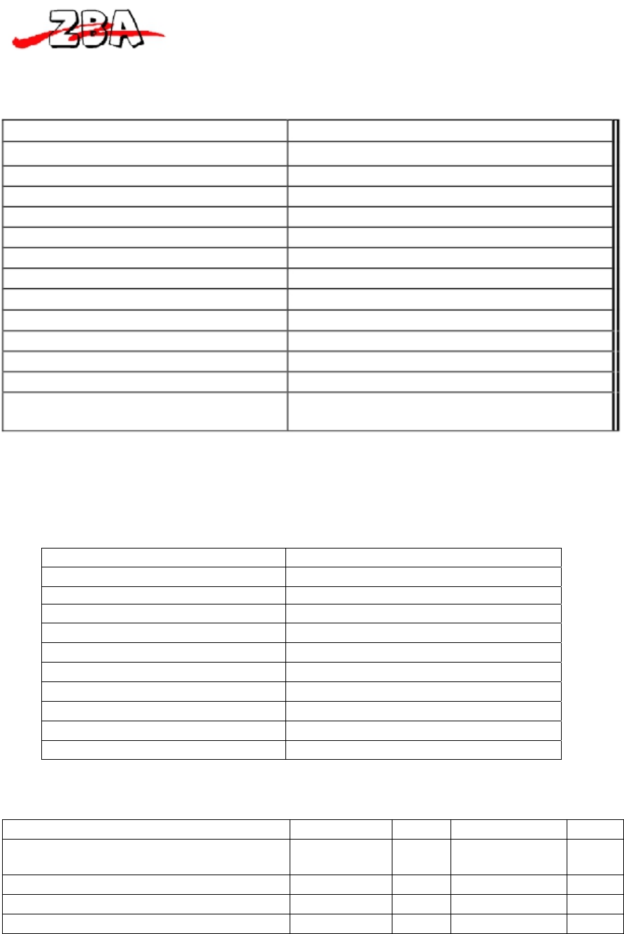
Voltage
Supply Voltage Range -0.3 to 3.6 V
Voltage at digital pins -0.3 to 3.6 V
Storage Conditions
Storage Temperature -10°C to 70°C (ambient)
Storage Humidity 0-90% RH
Operating Conditions
Temperature Range -0°C< TA<60°C
Peak Power supply current 150 mA
Relative humidity 5% to 95% non condensing
Digital Terminals Min Typ Max Units
Input Voltage Levels
VIL input logic level low2.7V = VDD = 3.0V -0.4 +0.8 V
VIH input logic level high - 0.7VDD VDD+0.4 V
Output Voltage Levels
ZBA, Inc.
8 General Specifications
Item
Carrier Frequency
Modulation
Channel Intervals
Number of Channels
Frequency Hopping
Receive Sensitivity
Transmission Power
Maximum Data Throughput
Output Interface
Power Supply
Operating Temperature Range
Storage Temperature Range
Antenna
Specification
2400MHz to 2483.5MHz
GFSK, 1Mbps, 0.5BT Gaussian
1MHz
79
1600hops/sec, 1MHz channel space
-82 dBm typ. @0.1% BER
+18dBm max.
Asynchronous : 3 Mbps
Full speed UART,
3.3V ±10%
-20°C to 85°C
-40°C to 85°C
50 ohm external antenna required ( not part of
the module)
8.1 Electrical Characteristics
8.1.1 Absolute Maximum Ratings
Absolute maximum ratings for supply voltage and voltages on digital and analog pins of the
Module are listed below; exceeding these values will cause permanent damage
8.1.2 Input/Output Terminal Characteristics
Page 11

VOL output logic level low
(lo = 4.0mA), 2.7V = VDD = 3.0V
- 0.2 V
VOH output logic level high
(lo = -4.0mA), 2.7V = VDD = 3.0V
VDD-
0.2
V
Input and Tri-state Current with:
Strong pull-up -100 -40 -10 µA
Strong pull-down +10 +40 +100 µA
Weak pull-up -5.0 -1.0 -0.2 µA
Weak pull-down +0.2 +1.0 +5.0 µA
I/O pad leakage current I -1 0 +1 µA
CI Input Capacitance 1.0 - 5.0 pF
USB Terminals Min Typ Max Units
VDD_USB for correct USB operation(1) 3.1 3.6 V
Input threshold
VIL input logic level low - - - 0.3VDD_USB V
VIH input logic level high 0.7VDD_USB - - V
Input leakage current
VSS_PADS < VIN < VDD_USB(1) -1 1 5 µA
CI Input capacitance 2. 5 - 10.0 pF
Output Voltage levels To correctly
terminated USB Cable
VOL output logic level low 0.0 - 0.2 V
VOH output logic level high 2.8 - VDD_USB V
Description Min Typ MAX Bluetooth
Specification Units
Maximum RF transmit power
(3)
14 (4)
- 0 to +20 dBm
Variation in RF power over
temperature range with
compensation disabled (±)
2.0 - - dB
Variation in RF power over
temperature range with
compensation enabled (±)
1.0 dB
RF power control range >20 >16 dB
RF power range control
resolution 0.5 - dB
ZBA, Inc.
8.2 Radio Characteristics: Basic Data Rate
8.2.1 Transmitter
(Temperature =20oC)
Page 12

20dB bandwidth for
modulated carrier - 670 ≤1000 kHz
Adjacent channel transmit
power F=F0 ±2MHz -35 ≤-20 dBm
Adjacent channel transmit
power F=F0 ±3MHz - -40 ≤-40 dBm
Adjacent channel transmit
power F=F0>±3MHz - -47 ≤-40 dBm
Δf1avg Maximum
Modulation
159 140<? f1avg<175 kHz
Δf2max Minimum
Modulation
123 - ≥115 kHz
Δf2avg / ?f1avg - 0.84 ≥0.80 - -
Initial carrier frequency
tolerance - 6.0 ±75 KHz
Drift Rate 8.0 ≤20 kHz/50µs
Drift (single slot packet) 9.0 ≤25 - kHz
Drift (five slot packet) 11.0 ≤40 kHz
nd
2 Harmonic content -43 ≤- 30 dBm
rd
3 Harmonic content -34 ≤- 30 dBm
Frequency (GHz ) Min Typ MAX Bluetooth
Specification Units
2.402 - -86.5 - ≤-70 dBm dBm
2.441 -86.5
Sensitivity at 0.1% BER for
all packet types
2.480 -87
Maximum received signal at
0.1% BER - >-20 ≥-20 dBm
Frequenc
y
(
MHz
)
Min T
y
pMA
X
Bluetooth Units
ZBA, Inc.
Notes:
(1) The design is capable of producing 18dBm at 20°C. However, in order to meet both the FCC Part 15.205a
and 15.209a radiated spurious requirement of -41dBm/MHz (500microvolts/metre at a distance of 3
meters) and the Bluetooth requirement for ACP, it is necessary to limit the maximum output power to
+14dBm at 20°C. The corresponding recommended POWER_TABLE entry is internal gain 55, external
gain 170.
(2) Class 1 RF transmit power range, Bluetooth specification v2.0 + EDR.
(3) To some extent these parameters are dependent on the matching circuit used and its behaviour over
temperature. Therefore, these parameters may be beyond CSR’s direct control.
(4) Resolution guaranteed over the range -5dB to -25dB relative to maximum power for Tx Level >20.
(5) Measured at F0 = 2441MHz.
(6) Up to three exceptions are allowed in v2.0 + EDR of the Bluetooth specification. BlueCore4-External is
guaranteed to meet the ACP performance as specified by the Bluetooth specification v2.0 + EDR.
(7) Measurement made using a POWER_TABLE entry of internal gain 55, external gain 170. This ensures
that the Bluetooth requirements and those defined by the FCC and ETSI are satisfied over the operating
temperature range of -20°C to +65°C. Measured using an operating output power of 14dBm at 20°C.
8.2.2 Basic Data Rate---Receiver
Page 13
(Temperature =20oC)

Specification
30 –
2000 >0 -10 dBm
2000
–
2400
- >-15 -27
Continuous power required
to block Bluetooth
reception (for sensitivity of -
67dBm with 0.1%
BER). Measured at the
antenna connection. 2500
–
3000
>-18 -27
C/I co-channel -9 ≤11 dB
Adjacent channel selectivity
C/I F=F0 +1MHz -4 ≤0 dB
Adjacent channel selectivity
C/I F=F0 - 1MHz -2 ≤0 dB
Adjacent channel selectivity
C/I F=F0 +2MHz -38 ≤-30 dB
Adjacent channel selectivity
C/I F=F0 - 2MHz -21 ≤-20 dB
Adjacent channel selectivity
C/I F=F0 ?+3MHz -43 - ≤ -40 dB
Adjacent channel selectivity
C/I F=F0 - 5MHz - -43 ≤-40 dB
Adjacent channel selectivity
C/I F=FImage
-21 <-9 dB
Maximum level of inter-
modulation interferers -37 ≥-39 dBm
Spurious output level -140 - dBm/Hz
Description Min Typ Max Bluetooth
Specification units
Maximum RF transmit power 18(2) - 0 to +20 (3) dBm
Relative transmit power -2 -4 to +1 dB
π/4 DQPSK
Max carrier frequency stability w0
1.5 ≤±10 for
all blocks
kHz
π/4 DQPSK
Max carrier frequency stability wi
6.6 - ≤ ±75 for
all packets
kHz
ZBA, Inc.
Notes:
(1) Up to five exceptions are allowed in v2.0 + EDR of the Bluetooth specification. BlueCore4-External is
guaranteed to meet the C/I performance as specified by the Bluetooth specification v2.0 + EDR
(2) Measured at F0 = 2441MHz
(3) Measured at f1-f2 = 5MHz. Measurement is performed in accordance with Bluetooth RF test RCV/CA/05/c,
i.e. wanted signal at -64dBm
(4) Measured at the antenna connection. Integrated in 100kHz bandwidth and then normalized to 1Hz.
Bluetooth band of frequencies, with exceptions of -84dBm at 1625MHz, -76dBm at 2435MHz, and
-68dBm at 3200MHz.
8.2.3 Radio Characteristics: Enhanced Data Rate
8.2.3.1 Transmitter (Temperature = +20°C)
Page 14

π/4 DQPSK
Max carrier frequency stability
¦w0 + wi¦
7.0 ≤±75 for
all blocks
kHz
8DPSK
Max carrier frequency stability w0
1.5 - ≤ ±10 for
all blocks
kHz
8DPSK
Max carrier frequency stability wi 4.5 ≤±75 for
all packets
kHz
8DPSK
Max carrier frequency stability
¦w0 + wi¦
5.0 ≤±75 for
all blocks
kHz
π/4 DQPSK Modulation Accuracy
RMS DEVM 7.0 - ≤ 20 %
99% DEVM 12.0 ≤30 %
Peak DEVM 16.0 ≤35 %
8DPSK Modulation Accuracy
RMS DEVM 8.0 - ≤13 %
99% DEVM 13.0 ≤20 %
Peak DEVM 16.0 ≤25 %
In-band spurious emissions
F > Fo+3MHz - -45 ≤-40 dBm
F < Fo -3MHz -45 ≤-40 dBm
F = Fo -3MHz(6) -38 ≤-40 dBm
F = Fo -2MHz -25 ≤-20 dBm
F = Fo –1MHz -36 ≤-26 dB
F = Fo +1MHz -36 ≤-26 dB
F = Fo +2MHz -25 ≤-20 dBm
F = Fo +3MHz(6) -28 ≤-40 dBm
EDR Differential Phase Encoding
No
Errors =99 %
ZBA, Inc.
Notes:
(1) BlueCore4-External firmware maintains the transmit power to be within the Bluetooth v2.0 + EDR
specification limits.
(2) Although the design is capable of generating in excess of +18dBm, regulatory compliance over the full
temperature range of -20°C to +65°C will not be satisfied if the transmit power approaches this value.
Actual output power with TX_PRE 71, INT PA 63, EXT PA 255 corresponds to +8dBm at 20°C.
Page 15

Description Min Typ. Max Bluetooth
specification Units
Sensitivity at 0.01% BER
π/4 DQPSK - -89 - ≤-70 dBm
8DPSK - -82 - ≤-70 dBm
Maximum received signal at
0.1% BER
π/4 DQPSK - >0 - ≥-20 dBm
8DPSK - -10 - ≥-20 dBm
C/I co-channel at 0.1% BER
π/4
DQPSK
- 10 - ≤+13 dB
8DPSK - 18 - ≤+21 dB
Adjacent channel selectivity C/I
F=F0 +1MHz -11 ≤0
π/4 DQPSK - - dB
8DPSK - -5 - ≤
+5
dB
Adjacent channel selectivity C/I
F=F -1MHz
π/4 DQPSK - - -8 - ≤0 dB dB
8DPSK - -4 - ≤+5 dB
Adjacent channel selectivity C/I
F=F dB 0 +2MHz
π/4 DQPSK - -43 - ≤-30 dB
8DPSK - -38 - - ≤ -25 dB
Adjacent channel selectivity C/I
F=F dB 0 -2MHz
ZBA, Inc.
(3) Class 1 RF transmit power range, Bluetooth v2.0 + EDR specification.
(4) Measurements methods are in accordance with the EDR RF Test Specification v2.0.E.2.
(5) Modulation accuracy utilizes Differential Error Vector Magnitude (DEVM) with tracking of the carrier
frequency drift.
(6) The Bluetooth specification values are for 8DPSK modulation. Up to three exceptions are allowed in the
Bluetooth v2.0 + EDR specification. BlueCore4-External is guaranteed to meet the ACP performance as
specified by the Bluetooth v2.0 + EDR specification.
8.2.3.2 Receiver (Temperature = +20°C)
Page 16

π/4 DQPSK - -22 - ≤-20 dB
8DPSK - - 22 - ≤-13 dB
Adjacent channel selectivity C/I
F=F dB 0 +3MHz
π/4 DQPSK - -46 - ≤-40 dB
8DPSK - -42 - ≤-33 dB
Adjacent channel selectivity C/I
F=F dB 0 –5MHz
π/4 DQPSK - -43 - ≤
-40
dB
8DPSK - -40 - - ≤ -33 dB
Adjacent channel selectivity C/I
F=F dB Image
π/4DQPSK - -21 - ≤-7 dB
8DPSK - -14 - ≤0 dB
ZBA, Inc.
Notes: (1) Measured at F0 = 2405MHz, 2441MHz, 2477MHz
Page 17
ZBA, Inc.
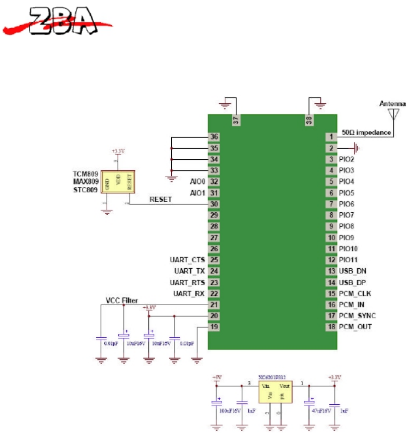
9 Typical Application Circuit
Figure 5 Schematic of typical application circuit
Page 18

ZBA, Inc.
10 Serial Port Profile
When shipped with the pre-programmed Serial Port Profile (SPP), the module’s firmware
emulates the function of a serial port. When connected to the host microprocessor via the
UART transport, the module appears as a COM port. This makes it easy for designers to
write software to utilize Bluetooth wireless communication. The SPP profile embedded
within the module provides a menu for making configuration changes utilizing AT
commands described below in section 10.2:
10.1 Default Configuration
•
•
•
•
•
•
•
•
•
•
UART Baud Rate: 9600 baud
Number of Bits: 8
Stop bit: One
Parity: None
H/W Flow Control: Disable
PIN: 1111
Device Name: ZBA-SPP
Mode: Slave
Sleep Mode: Deep sleep whenever possible.
Partner pairing is dropped at power off or un-pairing by master.
10.2 Configuration Commands Set-up & Procedures
PC interface: If you wish to connect the module to a PC’s comm. port it is necessary to
include a level shifter between the module and the PC. A recommended interface IC would
be the MAX3232 RS232 driver IC (or equiv.) and a 3.3 Volt voltage regulator.
Please contact ZBA for details on purchasing an evaluation board to ease the interface the
module to the PC.
Microcontroller Interface: The UART of the Bluetooth module can directly connect to the
microprocessors UART. The Microprocessor must have an I/O that will operate from 0 to
3.3 Volts or the appropriate level shifter circuitry must be used as to not overstress the I/O
of either device.
Entering Command Mode:
. For modules to enter in the command mode, the host must send a single character ESC
<0x1B> within 5 second after the unit has been powered on. If the ESC character is not
sent within the specified 5 second window then the module will automatically enter the SPP
mode and any information sent to the UART will be treated as data to be transmitted over a
Bluetooth link. Please note. The modules will only respond to the host set-up commands
Page 19

Command Response Parameter
ESC <CR>
+OPEN:num<CR><LF> Num= 0: device is not paired
Num= 1 Device has a saved
BT Address in memory
Command Response Parameter
AT OK None
Command Response Parameter
ATZ? List of Commands None
ZBA, Inc.
after the module has entered the command mode
Entering the SPP mode
After running any set-up commands then there are two ways to enter the SPP mode
a) Disconnect the 3.3 Volts supply to the module then re-power the module
and DO NOT hit the <ESC> key or send the <ESC> command. After 5
seconds the module will be in the SPP operation mode.
b) From the Set-up mode type: AT+EXIT
The module will respond with: OK
The module is now in SPP operation mode.
Note: All Commands except the first <ESC> command should contain a suffix of
<CR><LF>.
10.2.1
Entering the Set-up Mode
Note: If the device returns +open:0 and bind is disabled (bind=0) then the device is not
paired or connected and there is no remote device saved in the remote address
(+RADDR) variable If the device returns a +open:1 and the bind is enabled
(bind=1) then the module device is operating as a cable replacement function and it
will pair with the master Bluetooth device that is saved in the remote address
variable ASAP. The BT44-xxx module is bound to the companion device whose
address is saved in the + RADDR variable.
10.2.2
10.2.3
10.2.4
Testing the Communication Link
Command list
Set RS232 Baud Rate (bps)
Command Response
Page 20
Parameter

Command Response Parameter
AT+UARTMODE=<Para1>,<Para2> OK
AT+ UARTMODE? OK
UARTMODE:
<Para1>,<Para2>
<Para1>= Stop-bit
<Para1>
0 = 1 Stop bit
1 = 2 Stop bits
<Para2> Parity- bit
0 = None
1 = ODD
2 = EVEN
Command Response Parameter
AT+AUTH=<Para1> OK
AT+AUTH? OK
+AUTH:<Para1>
Para1 = Authentication
0 = disable
1= enable
Default mode:
Authentication enabled
Command Res
p
onse Parameter
AT+PASSWORD=
< Para1> OK
AT+PASSWORD? OK
+PASSWORD: < Para1>
Para1 Password
Default = 1111
Command Res
p
onse Parameter
AT+NAME= < Para1> OK
AT+NAME? OK
+NAME: <Para1>
Para1= Device name
Default= ZBA-SPP
ZBA, Inc.
Note: The default baud rate is 9600bps
10.2.5
Set/inquired UART Parameters
Note: the default UARTMODE parameters are N, 8, 1 and the overall comm.
Default Parameters are 9600,N,8,1
10.2.6
Set Authentication
Note: The default authentication mode is Authentication enabled.
10.2.7
Set Password
Note: The default authentication password = 1111.
10.2.8
Set Device Name
Page 21

AT+BAUD= <Para1> OK Para1 = 1200, 2400, 4800,
9600, 19200, 38400,
57600, 115200, 230400
AT+BAUD? OK
+BAUD: <para1>

Command Response Parameter
AT+SNIFFEX=<Para1>,<Para2>,
<Para3>,<Para4> OK
AT+SNIFFEX? OK
+SNIFFEX<Para1>,<Para2>,
<Para3>,<Para4>
Para1 Maximum
Para2 Minimum
Para3 test
Para4 Over time
Para5 Sniff timeout
Command Response Parameter
AT+SNIFF=<Para1>,<Para2>,
<Para3>,<Para4> OK
AT+SNIFF? OK
+SNIFF<Para1>,<Para2>,
<Para3>,<Para4>
Para1 Maximum
Para2 Minimum
Para3 test
Para4 Over time
Command Response Parameter
AT+CLASS=< Para1> OK
AT+CLASS? OK
+CLASS:<Para1>
Para1 Device type (Length
must = 6 characters)
default = 000000
Command Res
p
onse Parameter
AT+ROLE=< Para1> OK
AT+ROLE? OK
+ROLE: <Para1>
Para1
Slave = 0, Master = 1
Default = 0, Slave
Command Response Parameter
AT+RESET OK None
ZBA, Inc.
Note: The default Device name = ZBA-SPP.
10.2.9
Set Device Type
10.2.10 Set Master/Slave Mode
Note: The default mode is Slave.
10.2.11 Set Sniff Power Saving Mode
Note: Default = 1024, 512, 1024, 512 number in decimal mode
10.2.12 Set Sniff Power Saving Mode—Extended
Note: Default = 1024, 512, 1024, 512, 10 number in decimal mode
10.2.13 Reset to Factory Default
10.2.14 Set/Inquire Scan Time
Command Response
Page 22
Parameter

AT+SCANTIME=<Para1>,<Para2>,
<Para3>,<Para4> OK
AT+SCANTIME? OK
+SCAN :<Para1>,<Para2>,
<Para3>,<Para4>
Para1= Scan interval
tim
Para2=Scan time-out
Para3=Inquiry interval
Para4=Inquiry time-out
Command Response Parameter
AT+BIND=
< Para1> OK
AT+BIND? OK
+BIND:<Para1>
Para1
0 = Drop pair
1 =Always paired
Default=0 Drop pairing
Command Response Parameter
AT+CLEARADDR OK None
ZBA, Inc.
Note: The Default Values (in decimal = N* 625 us)
Para1 = 2048
Para2 = 18
Para3 = 2048
Para4 = 18
10.2.15 Set/Inquire Paired Device
Note: The default mode is to drop pair. The drop pair function occurs when the module
(slave or master mode) is power-off then back on or the master drops pairing. This will
allow another master to commence a discovery process and connect to the module (slave)
device.
If the device is set-up as always paired (bind=1) then the module will only communicate
with the specific slave (or master) whose address it has been bound to even after power off
and power-on. This mode is useful for application where a cable replacement function is the
requirement. To communicate to a different master, the module must have the bound
address cleared. This is accomplished by running the AT+CLEARADDR command.
If a module has been operated with bind=1 and then subsequently the bind function is set to
0, the module will still remember the previous bound address. So if bind is re-enabled then
device will re-connect to the previously bound master. To clear the memory please run the
AT+CLEARADDR command.
10.2.16 Clear Paired Device Address
Note: This command will clear any remote device address to which the module has been
paired.
Page 23

Command Response Parameter
AT+INQ OK +
BT address, Device name
Command Response Parameter
AT+RADDR=<Para1> OK
AT+ RADDR? OK
+RADDR:<Para1>
Para1= Paired device BT
address
Command Response Parameter
AT+VERSION? OK
+VERSION:<Para1> Para1 version #
Command Res
p
onse Parameter
AT+CANCEL? OK
ZBA, Inc.
10.2.17 Inquire Version
Note: This command will return the firmware version of the module.
10.2.18 Inquire Remote Device Address
Note: This command commences the discovery process to detect any BT device in the
neighborhood. Completion of this command may take up to 30 seconds.
An example of the response to the above command is: +INQRESU:0005164801E6, ZBA-
SPP where the data following the colon is one example of the Bluetooth address of one of
the devices in the neighborhood and the data following the comma is the name of the
discovered device.
10.2.19 Set/Inquire Paired Device Address
Example of how to pair using the BT44-191 as the Master
Example to set-up the Module to communicate with one specific BT device whose BT
address is currently unknown.
First type: AT+INQ which causes the Module to return the BT addresses of the devices in
the BT neighbourhood. Then the module will return +INQCOMP. This response will
indicate that the Inquiry process has terminated.
To terminate the AT+INQ command early, please type the command AT+CANCEL
Then type AT+RADDR= BT address (the specific device you wish to pair as determined
from the AT+INQ Command).
.
The module will remain bound to this address until the AT+CLEARADDR (command
8.2.16) is run or the module is powered off and then back on again.
10.2.20 Cancel Inquiry
Page 24

Command Response Parameter
AT+ DATAMODE=<Para1> OK <Para1>:
0:Data is held in buffer, & it will be
sent to the other device after successfully
connect.
1:Data will be deleted after the BT
devices have been disconnected.
AT+ DATAMODE? OK
+DATAMODE:<Para1>
Command Response Parameter
AT+LOWPOWER=<Para1> OK <Para1>:
0: low power disabled
1:Low power mode Enabled
AT+ LOWPOWER? OK
+LOWPOWER:<Para1>
Command Response Parameter
AT+
FLOWCONTROL=<Para1> OK <Para1>:
0: No Flowcontrol
1:Use hardware
Flowcontrol
Command Response Parameter
AT+LADDR? OK
+LADDR:<Para1> Para1
Device address
ZBA, Inc.
+INQCOMP
Note: This command will cancel the inquiry command (AT+INQ).
10.2.21 Inquire Device BD Address
Note: This command returns the (local) BT address of the module.
10.2.22 Software Reset
10.2.23 Set/Inquire about Low power mode
Note: the default value for Low power =0
10.2.24 Set/Inquire Data processing mode at BT disconnect
Note: the default value for Datamode =0
10.2.25 Set/Inquire about Flow control mode (Handshaking)
Page 25

Command Res
p
onse Parameter
AT+ RESTART OK None
Command Response Parameter
AT+EXIT OK None
ZBA, Inc.
AT+ FLOWCONTROL? OK
+FLOWCONTROL:<Para1>
Note: the default value for Flowcontrol =0
10.2.26 Exiting the Set-up Mode
Note: This command returns the module to SPP mode.
11 Low Power Modes
11.1 Park & Sniff
The module will automatically go into a reduced power mode if there is no UART activity
and no RF activity. The Device will sniff in order to maintain synchronization with the
Master.
To save maximum power then it is possible to completely turn-off the power to the module.
When operating in this mode the Master/ Slave must then proceed through the Discovery
phase (consuming time and energy) before a connection can be re-established. This mode is
only recommended if there are very, very long periods of inactivity and the battery power is
of the utmost concern.
Page 26
ZBA, Inc.
12 Mounting Recommendations
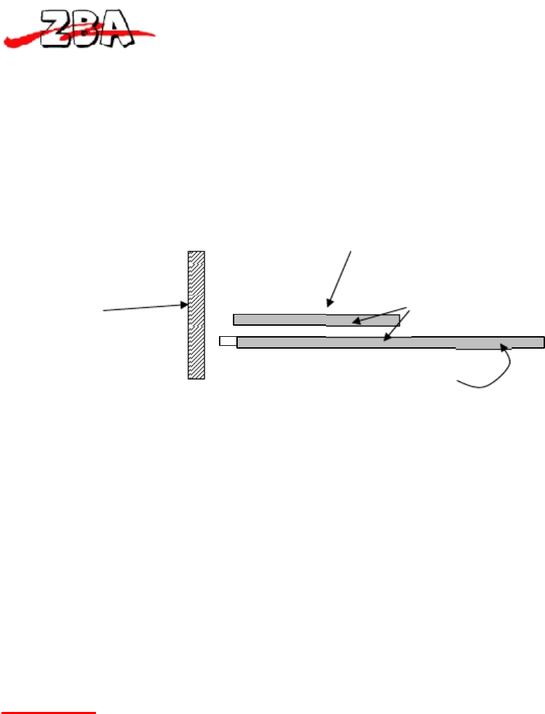
For maximized performance please orient the device with the antenna as close to the
antenna connector as possible. Best performance will occur if the underlying PCB has a
ground plane under the module.
BT module
Plastic
Ground Planes
Housing
Host PCB
Side View
Figure 6 Cross-section of recommended mounting of the BT module
13 Solder Profiles
WARNING : Contact ZBA if you wish to reflow the Modules in your production
environment. There are specific configurations that need to be reviewed with the
production facility to allow for proper reflow of the modules. Typically sample quantities of
the modules are hand soldered! Small quantities of modules should be hand soldered to the
main PCB.
When ordering PRODUCTION QUANTITES please CONTACT ZBA to make sure that
the modules have the correct configuration for Reflow processing.
The solder profile is available upon request.
Page 27

Orderin
g
P/N Descri
p
tion
BT44-191S-XXX Class 2 Module with Onboard Antenna
XXX = SPP Serial Port Profile
= HCI Host controller Interface over UART
= HID Human Interface device
= OOX Object push/ pull and FTP
BT44-147S-XXX Class 2 Bluetooth Module requires External Antenna
XXX = SPP Serial Port Profile
= HCI Host controller Interface over UART
= HID Human Interface device
= OOX Object push/pull and FTP
Ordering P/N Description
BT44-111S-XXX Class 1 Bluetooth Module requires an External Antenna
XXX = SPP Serial Port Profile
= HCI Host controller Interface over UART
= HID Human Interface device
= OOX Object push/ pull and FTP
ZBA, Inc.
14 Ordering Information
Other Solder down Bluetooth module variants
Please contact ZBA Inc at 908-359-2070 for any other profiles that you may
require.
####
Page 28
Page 29
FCC ID statement
This equipment complies with Part 15 of the FCC Rules.
Operation is subject to the following two conditions:
(1) This device may not cause harmful interference, and
(2) This device must accept any interference received, including interference that may
cause undesired operation.
Any changes or modifications not expressly approved by the party responsible for
compliance could void the user's authority to operate this equipment.
IC ID statement
Disclaimer:
Operation is subject to the following two conditions:
(1) This device may not cause interference, and
(2) This device must accept any interference, including interference that may cause
undesired operation of the device.
RF exposure warning
This equipment must be installed and operated in accordance with provide instructions
and the antenna used for this transmitter must be installed to provide a separation distance
of at least 20 cm from all persons and must not be co-located or operation in conjunction
with any other antenna or transmitter. End-users and installers must be provide with
antenna installation instructions and transmitter operating conditions for satisfying RF
exposure compliance.
Information for the OEMs and Integrators
The following statement must be included with all versions of this document supplied to
an OEM or integrator, but should not be distributed to the end user.
This device is intended for OEM integrators only.
Please see the full grant of equipment document for other restrictions.
Information to be supplied to the end user by the OEM or Integrator
The following regulator and safety notices must be published in documentation supplied
to the end user of the product or system incorporating an adapter in compliance with local
regulation. Host system must be labeled as following:
“Contains transmitter module FCC ID: VMTB44-111S, IC ID: 8941A-BT44111S”