Users Manual

MG2636 modules
MG2636 Module User Manual
Version: V1.0
ZTE Corporation

MG2636 module
1
Copyright Statement
Copyright © 2010 by ZTE Corporation
All rights reserved.
No part of this publication may be excerpted, reproduced, translated or utilized in any form or by any means,
electronic or mechanical, including photocopying and microfilm, without the prior written permission of ZTE
Corporation.
is the registered trademark of ZTE Corporation. All other trademarks appeared in this manual
are owned by the relevant companies.
ZTE Corporation reserves the right to make modifications on print errors or update specifications in this
manual without prior notice.
ZTE Corporation keeps the right to make the final explanation to this manual.

MG2636 module
2
With strong technical force, ZTE Corporation can provide CDMA/GPRS module customers with the following
all-around technical support:
1. Provide complete technical documentation;
2. Provide the development board used for R&D, test, production, after-sales, etc.;
3. Provide evaluations and technical diagnosis for principle diagram, PCB, test scenarios;
4. Provide test environment;
ZTE Corporation provides customers with onsite supports, and also you could get supports through telephone,
website, instant communication, E-mail, etc.
The module website module.ztemt.com.cn provides the relevant industry information and module
technical documentation. The authorized module customers could download the latest technical
documentation for our website. If you have more requirements, you could send an E-mail to
module@zte.com.cn. You can also call us at 0755-86360280 for more supports.
MG2636 module
3
Preface
Summary
This user manual is for MG2636 modules. It takes MG2636 modules for example to give the reference to the
relevant hardware design and instruct the users how to quickly and conveniently design different kinds of
wireless terminals based on this type of module.
Target Readers
System designing engineers
Mechanical engineers
Hardware engineers
Software engineers
Test engineers
Brief Introduction
This manual contains 5 chapters. See the table below:
Chapter Contents
1 General description Introduces MG2636 module’s basic technical specification, the relevant
documents for reference and the acronyms.
2 Product introduction Introduces MG2636 module’s principle diagram.
3 PIN definitions Introduces the name and function of MG2636 module’s Pins.
4 Description of hardware
interfaces
Introduces the design of the hardware interface on each part of MG2636
module.
5 Mechanical Design Introduces MG2636 module’s appearance diagram, assembly diagram and
PCB layout diagram.
6 Antenna Interface Introduce MG2636 Antenna Interface.
Update History
V1.0(2010-10-09)
This is the first time to officially release the document.

MG2636 module
4
Contents
1 General Description ...................................................................................................................................... 7
1.1 Technical Specification ................................................................................................................................. 7
1.1.1 Module’s Specification ..................................................................................................................... 7
1.1.2 Basic Functions ................................................................................................................................ 7
1.1.3 Module’s Interfaces .......................................................................................................................... 7
1.1.4 Technical parameters ........................................................................................................................ 8
1.2 Relevant Documents ..................................................................................................................................... 9
1.3 Acronyms ...................................................................................................................................................... 9
2 Product Introduction ................................................................................................................................... 12
3 PIN Definitions .......................................................................................................................................... 13
4 Decription of Hardware Interfaces ......................................................................................................... 15
4.1 Summary ..................................................................................................................................................... 15
4.2 Power and Reset ......................................................................................................................................... 15
4.2.1 Power Design ................................................................................................................................. 15
4.3 COM Port ................................................................................................................................................... 16
4.4 SIM Card Interface ..................................................................................................................................... 17
4.5 Audio Interface ........................................................................................................................................... 18
4.6 PCM Interface ............................................................................................................................................. 19
4.7 USB2.0 Interface ........................................................................................................................................ 20
4.8 Antenna Interface ........................................................................................................................................ 25
5 Mechanical Design .................................................................................................................................... 21
5.1 Appearance Diagram .................................................................................................................................. 21
5.2 Module Assembly Diagram ........................................................................................................................ 22
5.3 Module’s Fixing Method ............................................................................................................................ 22
6 Antenna Interface……………………………………………………………….………………………..24
6.1 Antenna Installation……………………………………………………………………………….…24
6.2 Antenna Pad…………………………………………………………………………………….……24
6.3 Antenna Connector…………………………………………………………………….…………..…24
6.4 Antenna Subsystem…………………………………………………………………………..………25
Important compliance information for North American users……………..………..……………………..26

MG2636 module
5
Graphics
Figure 2-1 MG2636 Function Block Diagram .................................................................................................... 12
Figure 3-1 PIN Definitions .................................................................................................................................. 13
Figure 4-1 UART Interface Reference Design Diagram ..................................................................................... 17
Figure 4-2 SIM Card Circuit Reference Design Diagram ................................................................................... 18
Figure 4-3 Audio Interface Circuit Refrence Design Diagram ........................................................................... 18
Figure 4-4 PCM Interface’s Time Sequence ..................................................................................................... 19
Figure 4-5 USB Interface Circuit Reference Design Diagram ............................................................................ 18
Figure 5-1 MG2636 Module’s Appearance ......................................................................................................... 21
Figure 5-2 Module’s Assembly Diagram ............................................................................................................ 22
Figure 6-3 Specification of MM9329-2700B connector………………………………………………………...24

MG2636 module
6
Tables
Table 1-1 Module’s specification ………………………………………………………………………………7
Table 1-2 Basic functions ………………………………………………………………………………………7
Table 1-3 Interfaces of the modules…………………………………………………………………………... 7
Table 1-4 Technical parameters ……………………………………………………………………………….8
Table 3-1 PIN definitions…………………………………………………………………………………….. 13
Table 3-1 PIN definitions…………………………………………………………………………………….. 13
Table 4-1 Voltage characteristics……………………………………………………………………………. 15
MG2636 module
7
1 General Description
This manual is applicable for MG2636 modules. With the function of voice, SMS and data service, ZTE
MG2636 module is a type of GSM/GPRS module developed by ZTE Corporation. MG2636 module could be
easily applied in modem, U-modem, embedded module, wireless phone, intelligent mobile phone, multimedia
mobile phone and touch screen telecom devices, etc.
Taking MG2636 module for example, this manual describes the module’s logic structure, hardware interface &
major functions, and provides references to the hardware and mechanical design.
1.1 Technical Specification
1.1.1 Module’s Specification
Please refer to table 1-1 for the module’s specification.
Table 1-1 Module’s specification
Models Format Frequency(MHz)
MG2636 GSM/GPRS GSM/GPRS:
GSM850/EGSM900/DCS1800/PCS1900*
*Note: EGSM900 and DCS1800 not support for North American market model, both band have been closed in
firmware.
1.1.2 Basic Functions
Please refer to Table 1-2 for the basic functions.
Table 1-2 Basic functions
Item Description
Voice call Circuit-switching service
Packet data Packet data service
SMS Support TEXT
1.1.3 Module’s Interfaces
Please refer to Table 1-3 for the module’s interfaces.
Table 1-3 Interfaces of the modules
MG2636 module
8
1.1.4 Technical parameters
Please refer to Table 1-4 for the module’s technical parameters.
Table 1-4 Technical parameters
Items Descriptions
Working temperature -30°C ~ +75°C
Input voltage 3.4V-4.25V
Maximum current 1800mA @ -102 dBm
Standby current (average) 10mA @ -75 dBm
Call current 230mA @ -75 dBm
Rx. Sensitivity -106.5dBm
Max. Tx power GSM850,EGSM900:33dBm(2W)
GSM1800,PCS1900:30dBm(1W)
Frequency range GSM850:
Tx: 824~849 MHz
Rx: 869~894 MHz
EGSM900
Tx: 880~915 MHz
Rx: 925~960MHz
DCS1800
Tx: 1710~1785MHz
Rx: 1805~1880MHz
PCS1900
Tx: 1850~1910MHz
Rx: 1930~1990MHz
Antenna Gain 2dBi
2. GSM/GPRS
Item GSM 850MHz/900MHz GSM 1800MHz/1900MHz
Out Power (GSM) 2W (+33dBm) 1W (+30dBm)
Interfaces Descriptions
Power interface Supply power to the module, reset the module or turn on/off the module
Audio interface Double audio I/O channel, one for differential, one for single end
SIM interface R-UIM
USB interface USB2.0 High Speed
UART interface Hardware full flow control port, customized by software
PCM interface Transmit voice data for Bluetooth applications
Antenna interface 50 Ohm input resistance control
MG2636 module
9
Out Power(EDGE) 500mW (+27dBm) 400mW (+26dBm)
Sensitivity <-102dBm <-102dBm
Frequency Error <0.1 PPM <0.1 PPM
Phane Error Max(°) ≤20 ≤20
RMS(°) ≤5 ≤5
1.2 Relevant Documents
《AT Command Manual for ZTE Corporation's MG2636 Modules》
《Wireless Module Test References》
1.3 Acronyms
A
ADC Analog-Digital Converter
AFC Automatic Frequency Control
AGC Automatic Gain Control
ARFCN Absolute Radio Frequency Channel Number
ARP Antenna Reference Point
ASIC Application Specific Integrated Circuit
B
BER Bit Error Rate
BTS Base Transceiver Station
C
CDMA Code Division Multiple Access
CDG CDMA Development Group
CS Coding Scheme
CSD Circuit Switched Data
CPU Central Processing Unit
D
DAI Digital Audio interface
DAC Digital-to-Analog Converter
DCE Data Communication Equipment
DSP Digital Signal Processor
DTE Data Terminal Equipment
DTMF Dual Tone Multi-Frequency
DTR Data Terminal Ready
E
EFR Enhanced Full Rate
MG2636 module
10
EGSM Enhanced GSM
EMC Electromagnetic Compatibility
EMI Electro Magnetic Interference
ESD Electronic Static Discharge
ETS European Telecommunication Standard
F
FDMA Frequency Division Multiple Access
FR Full Rate
G
GPRS General Packet Radio Service
GSM Global Standard for Mobile Communications
H
HR Half Rate
HSDPA High Speed Downlink Packet Access
I
IC Integrated Circuit
IMEI International Mobile Equipment Identity
ISO International Standards Organization
ITU International Telecommunications Union
L
LCD Liquid Crystal Display
LED Light Emitting Diode
M
MCU Machine Control Unit
MMI Man Machine Interface
MS Mobile Station
P
PCB Printed Circuit Board
PCL Power Control Level
PCS Personal Communication System
PDU Protocol Data Unit
PLL Phase Locked Loop
PPP Point-to-point protocol
R
RAM Random Access Memory
RF Radio Frequency
MG2636 module
11
ROM Read-only Memory
RMS Root Mean Square
RTC Real Time Clock
S
SIM Subscriber Identification Module
SMS Short Message Service
SRAM Static Random Access Memory
T
TA Terminal adapter
TDMA Time Division Multiple Access
TE Terminal Equipment also referred it as DTE
U
UART Universal asynchronous receiver-transmitter
UIM User Identifier Management
UMTS Universal Mobile Telecommunications System
USB Universal Serial Bus
V
VSWR Voltage Standing Wave Ratio
W
WCDMA Wide band Code Division Multiple Access
Z
ZTE ZTE Corporation
MG2636 module
12
2 Product Introduction
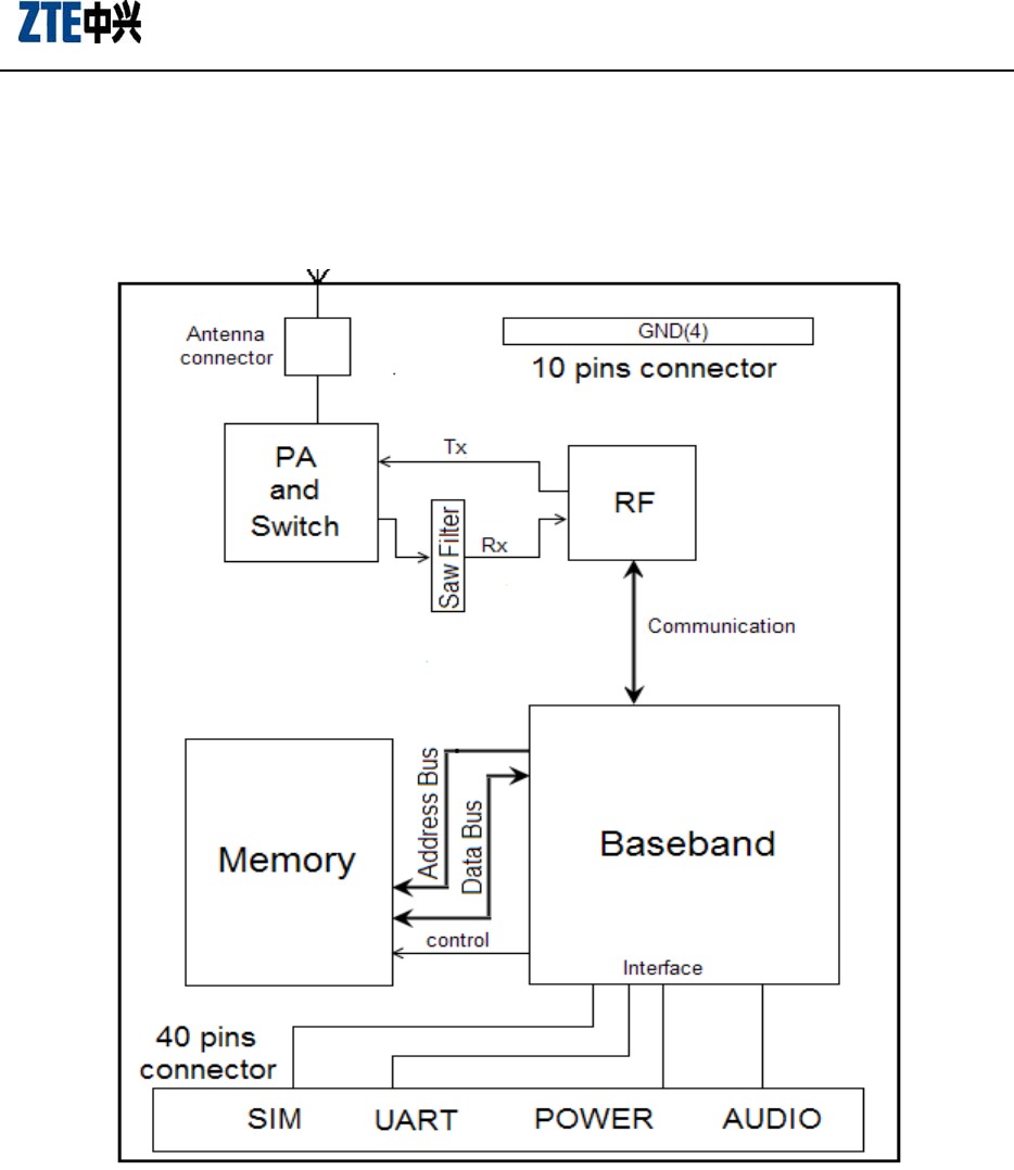
Please refer to Figure 2-1 for the function block diagram of MG2636.
Figure 2-1 MG2636 Function Block Diagram
MG2636 module is GSM/GPRS wireless module, MG2636 module adopts a 36PIN stamp hole, which is
applicable for GSM network. It supports 850/900/1800/1900 frequency band.
MG2636 module
13
3 PIN Definitions
MG2636 module adopts a 40PIN stamp hole and the distance between PINs is 0.5mm. Refer to table 3-1 below
for PIN definitions. Refer to table 3-2 for the key voltage of each pin.
Table 3-1 PIN definitions
1 VREG_USIM
UIM
MG2636MD_A
GND 36
2 SIM_RST
GND 35
3 SIM_CLK
LED
SIG_LED 34
4 SIM_DATA
PCM
PCM_DIN 33
5 GND
PCM_CLK 32
6 EAR2_P
AUDIO
USB
USB_DM 31
7 EAR1_P USB_DP 30
8 EAR1_N
ON/OFF 29
9 MIC2_P
UART
PCM_SYNC(/DS
R) 28
10 MIC1_P PCM_DOUT(DC
D) 27
11 MIC1_N /DTR 26
12 GND
/RTS 25
13 /PON_RESET
RI 24
14 VBUS
POWER
TXD 23
15 VCHG RXD 22
16 V_MAIN /CTS 21
17 V_MSME_1V8
GND 20
18 V_MAIN
ANT
RF_ANT 19
Refer to table 3-1 below for PIN definitions of MG2636 module.
Table 3-2 PIN definitions
Function Pin No. Signal name I/O Basic functions Remarks
SIM card
interface
1 VREG_USIM O 2.85V/1.8V
2 SIM_RST O USIM card reset signal
3 SIM_CLK O USIM card clock
4 SIM_DATA I/O USIM card data cable
Audio
6 EAR2_P O Single-end audio output
channel 2
7 EAR1_P O Differential audio output
channel 1, anode
8 EAR1_N O Differential audio output
channel 1, cathode
9 MIC2_P I Single-end audio input
channel 2
MG2636 module
14
10 MIC1_P I Differential audio input
channel 1, anode
11 MIC1_N I Differential audio input
channel 1, cathode
Reset 13 /PON_RESET I Reset signal Low level valid
Power
14 VBUS I USB power +5V
15 VCHG I Charge power
16 V_MAIN I Module’s main power 3.3V-4.2V
17 V_MSME_1V8 O Digital power Voltage output, 1.8V
18 V_MAIN I Module’s main power 3.3V-4.2V
29 ON/OFF I Power on/off control 1.8V, Low level valid
UART
21 /CTS I Clear to send 1.8V, Low level valid
22 RXD I Receive data 1.8V
23 TXD O Transmit data 1.8V
24 RI O Ring tone 1.8V
25 RTS O Request to send 1.8V, Low level valid
26 /DTR I Data terminal ready 1.8V, Low level valid
PCM
27 PCM_DOUT
(DCD) O PCM data output 1.8V, duplex with DCD
28 PCM_SYNC
(/DSR) O PCM frame SYNC clock 1.8V, duplex with
/DSR
32 PCM_CLK O PCM data clock 1.8V
33 PCM_DIN I PCM data input 1.8V
USB
interface
30 USB_DP I/O USB data+
31 USB_DM I/O USB data-
LED 34
SIG_LED O Module’s working status
LED
Antenna 19 RF_ANT I/O Antenna interface
GND
5、12、
20、35、
36
GND

MG2636 module
15
4 Decription of Hardware Interfaces
4.1 Summary
This chapter introduces each logic function interfaces of MG2636 module & its operation descriptions, and
provides the designing sample.
Power and Reset Interface
COM Port
SIM Card Interface
Audio Interface
PCM interface
USB2.0 interface
Antenna Interface
Remarks: In the system, the module layout should be far away from high-speed circuit, switch power, power
transformer, large power inductor, or single chip microcomputer’s clock circuit.
4.2 Power and Reset
4.2.1 Power Design
The module could work under two power modes: 1. Power adaptor; 2. Battery
The power could directly be supplied externally, the external power is added directly to V_MAIN and meets
the voltage requirements in table 4-1. The external power could be supplied by the power adaptor with constant
output, battery, USB power converter, etc. It’s recommended to design 2A current to meet the requirements of
GSM/GPRS.
Table 4-1 Voltage characteristics
Classification MIN. Typical Max.
Input voltage 3.3 V 3.8 V 4.25 V
Power on
The module will be turned off after power-on normally. To turn on the module, provide a 2000-2500mS
low level pulse to ON/OFF PIN.
Power off
To turn off the module, provide a 2500-4000mS low level pulse to ON/OFF PIN.
Reset
To reset the module, provide a 2500-4000mS low level pulse to ON/OFF PIN
After reset, the module will be turned off. To turn on the module, provide a 2000-2500mS low level
pulse to ON/OFF PIN.
V_MSME_1V8

MG2636 module
16
There is a voltage output pin with current adjuster on MG2636 module, which can be used to supply external
power to the board. The voltage of this pin and the voltage of baseband processor/memory come from the same
voltage adjuster. The voltage output is available only when the module is on. The normal output voltage is 1.8V,
and the user should absorb the current from this pin as little as possible (less than 10mA). Generally, it is
recommended to use this pin for pull-up when matching the level.
Other Advice
In order to make sure the data is saved safely, please don’t cut off the power when the module is on. It’s
strongly recommended to use ON/OFF pin or AT command to turn off the mobile phone.
4.3 COM Port
The module provides a full duplex UART interface, whose maximal data rate is 230.4kbps and typical data rate
is 11.5kbps. External interface is 1.8VCMOS level signal, which could be used for upgrade, port
communication, etc.
When using MG2636 module’s UART port to communicate with PC or MCU, please pay attention to the
direction of TX, RX. It’s specially noted that MG2636 module’s UART port only supports 1.8V, therefore for
non 1.8V external UART, it needs to convert the level. Normally a dynatron is used to realize the level
conversion. As shown in figure 4-1, the resistance is just for your information, please calculate again during the
design.

MG2636 module
17
Figure 4-1 UART Interface Reference Design Diagram
4.4 SIM Card Interface
The module supports 2.85V/1.8V SIM card, and it’s strongly recommended to add ESD component to protect
UIM card as shown in figure 4-2.
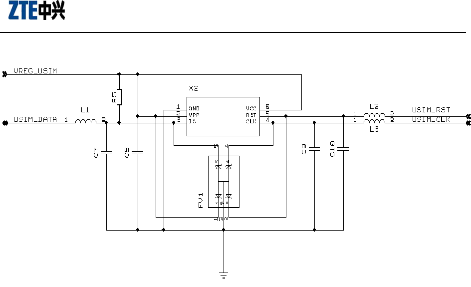
MG2636 module
18
Figure 4-2 SIM Card Circuit Reference Design Diagram
Note: The clock data rate of UIM card circuit is 4M, and the card socket should be laid closely around the
module and the wiring should be as short and thick as possible.
4.5 Audio Interface
The module provides 2 speaker interfaces and 2 microphone interfaces. Only one pair I/O works at the same
time.
Microphone
The two microphone interfaces MIC_N and MIC_P are differential interface, which could also be used for
single end input. It’s recommended to use differential mode to reduce the noises and it is directly connected with
the receiver. MIC_P is single ended interface, which could be directly connected to the microphone since the
offset voltage is internally provided.
Earpiece
The earpiece interface EAR1_P and EAR1_N are both differential interfaces with 32Ω resistance; EAR2_P is
single-ended interface with 32Ω resistance and no coupling of capacitor is required.
Design of audio interface on the receiver
Select the microphone with the sensitivity lower than -52dB since EAR1’s output power is 35mW and the max.
gain inside MIC1 reaches 52dB.
Note: if other kind of audio input method is adopted, the input signal should be within 1V. If the signal
voltage is lower than 1V, then the pre-amplifier should be added. If the signal voltage is higher than 1V,
then network attenuation should be added
Design of audio interface on the earpiece
Select the microphone with the sensitivity lower than -52dB since EAR2’s output power is 10.8mW and the
max. gain inside MIC2 reaches 52dB. The level of MIC2_P PIN is about 1.8V. The receiver’s design is just the
same as the receiver’s.
MG2636 module
19
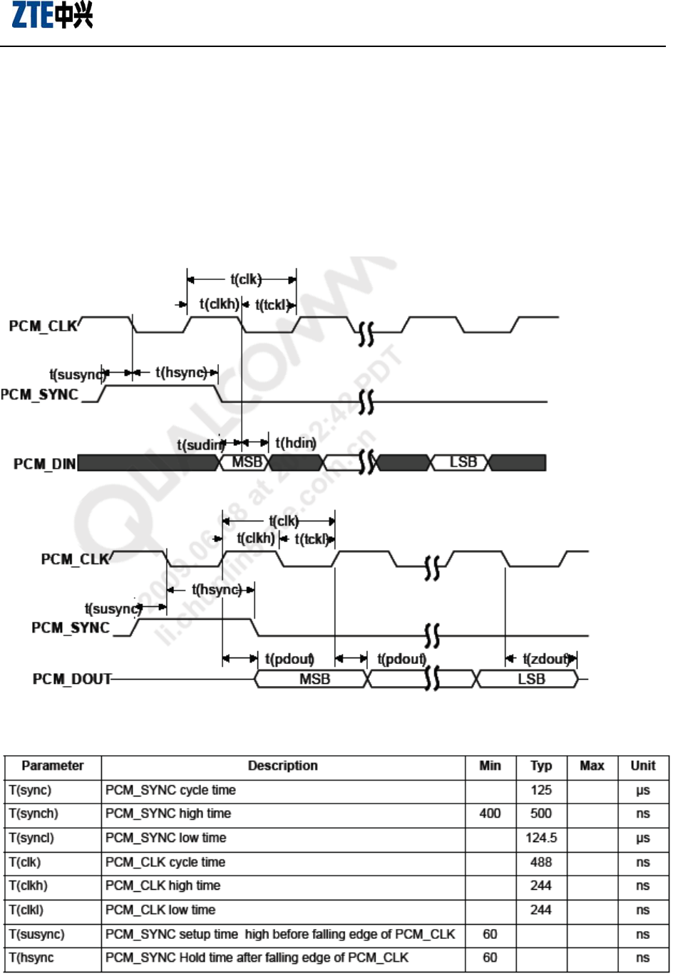
4.6 PCM Interface
The module’s PCM interface provides PCM_CLK, PCM_SYNC, PCM_DIN, PCM_DOUT,and it supports
2.048MHz PCM clock data rate and 8K frame data rate. PCM clock will stop the output when it enters the
dormant mode.
The module’s PCM interface must work under Master mode, and the clock and SYNC signal must be sent by
the module. The device connected with the interface can word under Slave mode only.
See the time sequence of PCM interface in figure 4-3.
Figure 4-3 Time Sequence of PCM Interface
MG2636 module
20
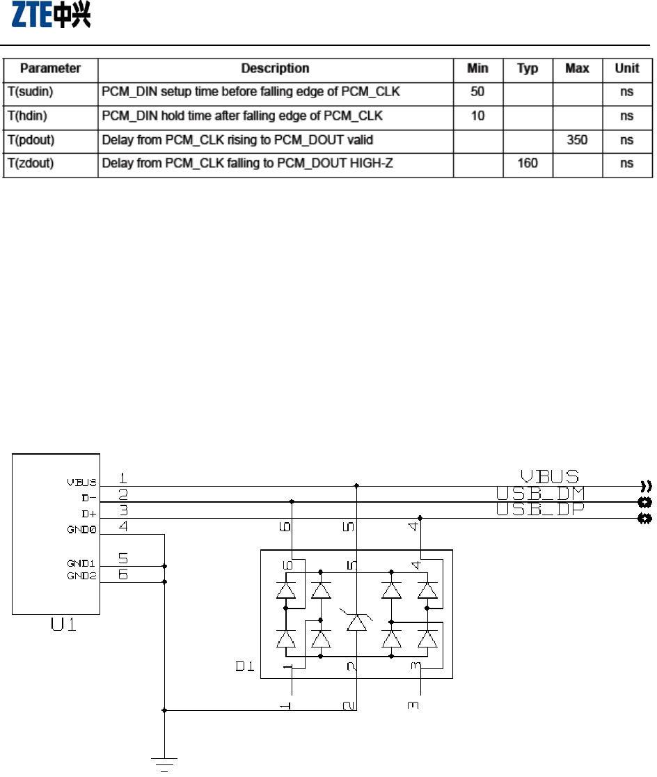
4.7 USB2.0 Interface
The module provides USB2.0 HS interface with 480Mbps, which is composed of VBUS, D+ and D-. You can
directly connect USB signal interface when designing the module’s external circuit, but try to add ESD
protector during the design to avoid damaging the module.
D1 is USB2.0 ESD protector in the figure, and the Junction capacitance is small than 3P. VBUS is connected to
the external host VBUS. The USB operating voltage is: 4.75—5.25V with the typical value of 5V. See figure
4-4.
Figure 4-4 USB Interface Circuit Reference Design Diagram
MG2636 module
21
5 Mechanical Design
5.1 Appearance Diagram
See the appearance of MG2636 module in figure 5-1.
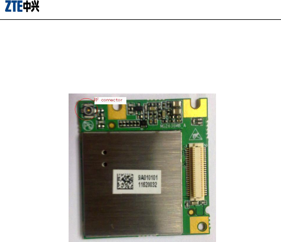
Figure 5-1 MG2636 Module’s Appearance
Dimensions:(LxWxH):35 mm x 32.5mm x2.65mm
Weight: 7g
MG2636 module
22
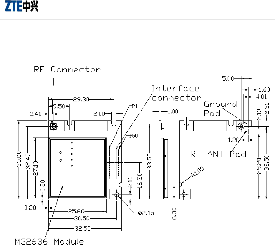
5.2 Module Assembly Diagram
See the assembly diagram of MG2636 module in figure 5-2.
Figure 5-2 Module’s Assembly Diagram
5.3 Module’s Fixing Method
The module’s fastening method adopts direct manual soldering to avoid second-time soldering. It’s strongly
recommend to use the manual soldering because MG2636 module board is just 0.8mm thick and MT6223BGA
space is too small.
MG2636 module
23
6. Antenna Interface
The RF interface of the MG2636 Module has an impedance of 50 . The module is capable of sustaining a
total mismatch at the antenna connector or pad without any damage, even when transmitting at maximum RF
power.
The external antenna must be matched properly to achieve best performance regarding radiated power,
DC-power consumption, modulation accuracy and harmonic suppression. Antenna matching networks are not
included on the MG2636 Module PCB and should be placed in the host application.
Regarding the return loss, the Module provides the following values in the active band:
Table 6-1 Return Loss in the Active Band
State of Module Return Loss of
Module Recommended Return Loss of
Application
Receive ≥ 8dB ≥ 12dB
Transmit not applicable ≥ 12dB
The connection of the antenna or other equipment must be de coupled from DC voltage. This is
necessary because the antenna connector is DC coupled to ground via an inductor for ESD protection.
6.1 Antenna Installation
To suit the physical design of individual applications, the MC2261 offers two alternative approached to
connecting the antenna:
■ Recommended approach: MM9329-2700B antenna connector manufactured by MURATA assembled on
the component side of the PCB (top view on Module). See Section 4.3 for details.
■ Antenna pad and grounding plane placed on the bottom side. See Section 4.2 for details.
The MM9329-2700B connector has been chosen as antenna reference point (ARP) for the ZTEMT
reference equipment submitted to type approve the MG2636 Module. All RF data specified throughout
this manual are related to the ARP. For compliance with the test results of the ZTEMT type approval
you are advised to give priority to the connector, rather than using the antenna pad.
Note: Both solutions can be applied alternatively. This means,if the antenna is connected to the pad, then
the connector on the Module must be left empty,and when the antenna is connected to the Module connector,
the pad is useless,
6.2 Antenna Pad
The antenna pad of the module is soldered to the board on the customer design to connect with RF line.
For proper grounding connect the RF line to the ground plane on the bottom of the MG2636 Module
which must be connected to the ground plane of the application.
Consider that according to GSM recommendations as 50Ω connector is mandatory for type approval
measurements. It must be ensured that the RF line which is connected to antenna pad should be controlled on
50Ω.
Notes on soldering
■ To prevent damage to the Module and to obtain long-term solder joint properties, you are advised to
maintain the standards of good engineering practice for soldering.
MG2636 module
24
Material Properties
■ MG2636 Module PCB: FR4
■ Antenna pad: Gold plated pad
6.3 Antenna connector
The MG2636 Module uses a microwave coaxial connector supplied by Murata Ltd. The product name
is MM9329-2700B. The position of the antenna connector on the Module PCB can be seen in Figure 6-3.
Figure 6-3 Specification of MM9329-2700B connector
Table 6-2 Product specifications of MM9329-2700B connector
Part
Number Rated
Voltag
e (V)
Contact
Resistan
ce
(ohm)
Withstandi
ng
Voltage
(rms)
Insulatio
n
Resistan
ce
(M ohm)
Durabili
ty
(cycles)
Frequen
cy
Rating
(GHz)
Temperatu
re
Range
(degree C)
VSWR Center
Conta
ct
Outer
Conta
ct
Insulator
MM9329
-2700B
250 0.015
max.
300 (AC) 500 min. 100 DC - 6.0 -40~+90. 1.2 max.
(DC~3GH
z)
Copper
Alloy
Gold
plated
Copper
Alloy
Silver
plated
Engineeri
ng plastic
6.4 Antenna Subsystem
The antenna sub-system and its design is a major part of the final product integration. Special attention and care
should be taken in adhering to the following guidelines.
6.4.1 Antenna Specifications
Choice of the antenna cable (type, length, performance, RF loss, etc) and antenna connector (type + losses) can
have a major impact on the success of the design.
6.4.2 Cable Loss
All cables have RF losses. Minimizing the length of the cable between the antenna and the RF connectors on

MG2636 module
25
the module will help obtain superior performance. High Quality/Low loss co-axial cables should be used to
connect the antenna to the RF connectors. Contact the antenna vendor for the specific type of cable that
interfaces with their antenna and ask them to detail the RF losses of the cables supplied along with the antenna.
Typically, the cable length should be such that they have no more than 1-2dB of loss. Though the system will
work with longer (lossy) cables, this will degrade GSM system performance. Care should also be taken to
ensure that the cable end
connectors/terminations are well assembled to minimize losses and to offer a reliable, sturdy connection to the
Module sub-system. This is particularly important for applications where the module is mounted on a mobile or
portable environment where it is subject to shock and vibration.
6.4.3 Antenna Gain Maximum Requirements
Our FCC Grant imposes a maximum gain for the antenna subsystem: 2 dBi for the GSM850 band and 2dBi for
the 1900 band.
Warning: Excessive gain could damage sensitive RF circuits and void the warranty.
6.4.4 Antenna Matching
The module’s RF connectors are designed to work with a 50-ohm subsystem. It is assumed that the antenna
chosen has matching internal to it to match between the 50-ohm RF connectors and the antenna impedance.
6.4.5 PCB Design Considerations
• The antenna subsystem should be treated like any other RF system or component. It should be isolated as
much as possible from any noise generating circuitry including the interface signals via filtering and shielding.
• As a general recommendation all components or chips operating at high frequencies such as
micro controllers, memory, DC/DC converts and other RF components should not be placed too close to the
module. When such cases exist, correct supply and ground de-coupling areas should be designed and validated.
• Avoid placing the components around the RF connection and close to the RF line between the RF antenna and
the module.
• RF lines and cables should be as short as possible.
• If using coaxial cable it should not be placed close to devices operating at low frequencies. Signals like
charger circuits may require some EMI/RFI decoupling such as filter capacitors or ferrite beads.
• Adding external impedance matching to improve the match to your cable and antenna assemblies is optional.
Please contact the antenna vendor for matching requirements.
• For better ESD protection one can implement a shock coil to ground and place it close to the RF connector.
Antenna Interface
Proper measures should be taken to reduce the access loss of effective bands, and good shielding should be
established between the external antenna and the RF connector. Besides, the external RF cables should be kept
far away from all interference sources such as high-speed digital signal or switch power supply.
According to mobile station standard, stationary wave ratio of antenna should be between1.1 to 1.5, and input
impedance is 50 ohm. Different environments may have different requirements on the antenna’s gain. Generally,
the larger gain in the band and smaller outside the band, the better performance the antenna has. Isolation
degree among ports must more than 30dB when multi-ports antenna is used. For example, between two
different polarized ports on dual-polarized antenna, two different frequency ports on dual-frequency antenna, or
among four ports on dual-polarized dual-frequency antenna, isolation degree should be more than 30dB.

MG2636 module
26
Important compliance information for North American users
The MG2636 Module has been granted modular approval for mobile applications. Integrators may use the
MG2636 Module in their final products without additional FCC certification if they meet the following
conditions. Otherwise, additional FCC approvals must be obtained.
1. At least 20cm separation distance between the antenna and the user’s body must be maintained at all times.
2. To comply with FCC regulations limiting both maximum RF output power and human exposure to RF
radiation, the maximum antenna gain including cable loss in a mobile-only exposure condition must not
exceed 2dBi in the cellular band and 2dBi in the PCS band.
3. The MG2636 Module and its antenna must not be co-located or operating in conjunction with any other
transmitter or antenna within a host device.
4. A label must be affixed to the outside of the end product into which the MG2636 Module is incorporated,
with a statement similar to the following: For MG2636: This device contains FCC ID: Q78-MG2636.
5. A user manual with the end product must clearly indicate the operating requirements and conditions that
must be observed to ensure compliance with current FCC RF exposure guidelines.
The end product with an embedded MG2636 Module may also need to pass the FCC Part 15 unintentional
emission testing requirements and be properly authorized per FCC Part 15.
Note: If this module is intended for use in a portable device, you are responsible for separate approval to
satisfy the SAR requirements of FCC Part 2.1093.