ZTE MG3732 WCDMA Wireless Data Terminal User Manual
ZTE Corporation WCDMA Wireless Data Terminal
ZTE >
User Manual

MG3732 modules
MG3732 Module User Manual
Version: V1.0
ZTE Corporation

MG3732 module
1
Copyright Statement
Copyright © 2010 by ZTE Corporation
All rights reserved.
No part of this publication may be excerpted, reproduced, translated or utilized in any form or by any means,
electronic or mechanical, including photocopying and microfilm, without the prior written permission of ZTE
Corporation.
is the registered trademark of ZTE Corporation. All other trademarks appeared in this manual
are owned by the relevant companies.
ZTE Corporation reserves the right to make modifications on print errors or update specifications in this
manual without prior notice.
ZTE Corporation keeps the right to make the final explanation to this manual.

MG3732 module
2
With strong technical force, ZTE Corporation can provide CDMA/GPRS module customers with the following
all-around technical support:
1. Provide complete technical documentation;
2. Provide the development board used for R&D, test, production, after-sales, etc.;
3. Provide evaluations and technical diagnosis for principle diagram, PCB, test scenarios;
4. Provide test environment;
ZTE Corporation provides customers with onsite supports, and also you could get supports through telephone,
website, instant communication, E-mail, etc.
The module website module.ztemt.com.cn provides the relevant industry information and module
technical documentation. The authorized module customers could download the latest technical
documentation for our website. If you have more requirements, you could send an E-mail to
module@zte.com.cn. You can also call us at 0755-86360280 for more supports.
MG3732 module
3
Preface
Summary
This user manual is for MC3732 modules. It takes MC3732 modules for example to give the reference to the
relevant hardware design and instruct the users how to quickly and conveniently design different kinds of
wireless terminals based on this type of module.
Target Readers
System designing engineers
Mechanical engineers
Hardware engineers
Software engineers
Test engineers
Brief Introduction
This manual contains 5 chapters. See the table below:
Chapter Contents
1 General description Introduces MG3732 module’s basic technical specification, the relevant
documents for reference and the acronyms.
2 Product introduction Introduces MG3732 module’s principle diagram.
3 PIN definitions Introduces the name and function of MG3732 module’s Pins.
4 Description of hardware
interfaces
Introduces the design of the hardware interface on each part of MG3732
module.
7 Mechanical design Introduces MG3732 module’s appearance diagram, assembly diagram and
PCB layout diagram.
Update History
V1.0(2010-09-01)
This is the first time to officially release the document.

MG3732 module
4
Contents
1 General Description ...................................................................................................................................... 7
1.1 Technical Specification ................................................................................................................................. 7
1.1.1 Module’s Specification ..................................................................................................................... 7
1.1.2 Basic Functions ................................................................................................................................ 7
1.1.3 Module’s Interfaces .......................................................................................................................... 7
1.1.4 Technical parameters ........................................................................................................................ 8
1.2 Relevant Documents ................................................................................................................................... 10
1.3 Acronyms .................................................................................................................................................... 11
2 Product Introduction ................................................................................................................................... 14
3 PIN Definitions .......................................................................................................................................... 14
4 Decription of Hardware Interfaces ......................................................................................................... 16
4.1 Summary ..................................................................................................................................................... 16
4.2 Power and Reset ......................................................................................................................................... 17
4.2.1 Power Design ................................................................................................................................. 17
4.3 COM Port ................................................................................................................................................... 18
4.4 UIM Card Interface ..................................................................................................................................... 18
4.5 Audio Interface ........................................................................................................................................... 19
4.6 PCM Interface ............................................................................................................................................. 20
4.7 USB2.0 Interface ........................................................................................................................................ 21
4.8 Antenna Interface ........................................................................................................................................ 22
5 Mechanical Design .................................................................................................................................... 23
5.1 Appearance Diagram .................................................................................................................................. 23
5.2 Module Assembly Diagram ........................................................................................................................ 24
5.3 Module’s Fixing Method ............................................................................................................................ 25

MG3732 module
5
Graphics
Figure 2-1 MG3732 Function Block Diagram .................................................................................................... 14
Figure 3-1 PIN Definitions .................................................................................................................................. 13
Figure 4-1 UART Interface Reference Design Diagram ..................................................................................... 18
Figure 4-2 UIM Card Circuit Reference Design Diagram .................................................................................. 19
Figure 4-3 Audio Interface Circuit Refrence Design Diagram ........................................................................... 19
Figure 4-4 PCM Interface’s Time Sequence ..................................................................................................... 21
Figure 4-5 USB Interface Circuit Reference Design Diagram ......................................... 錯誤! 尚未定義書籤。
Figure 5-1 MG3732 Module’s Appearance ......................................................................................................... 23
Figure 5-2 Module’s Assembly Diagram ............................................................................................................ 24

MG3732 module
6
Tables
Table 1-1 Module’s specification ………………………………………………………………………………7
Table 1-2 Basic functions ………………………………………………………………………………………7
Table 1-3 Interfaces of the modules…………………………………………………………………………... 8
Table 1-4 Technical parameters ……………………………………………………………………………….8
Table 3-1 PIN definitions…………………………………………………………………………………….. 15
Table 3-1 PIN definitions…………………………………………………………………………………….. 15
Table 4-1 Voltage characteristics……………………………………………………………………………. 17
MG3732 module
7
1 General Description
This manual is applicable for MG3732 modules. With the function of voice, SMS and data service, ZTE
MG3732 module is a type of WCDMA/HSDPA/GSM/GPRS/EDGE module developed by ZTE Corporation.
With the downlink peak data rate up to 3.6 Mbit/s and the uplink peak data rate up to 384 Kbit/s, the module
could provide economic high-speed Internet access and wireless data service. MG3732 module could be
easily applied in modem, U-modem, embedded module, wireless phone, intelligent mobile phone, multimedia
mobile phone and touch screen telecom devices, etc.
Taking MG3732 module for example, this manual describes the module’s logic structure, hardware interface &
major functions, and provides references to the hardware and mechanical design.
1.1 Technical Specification
1.1.1 Module’s Specification
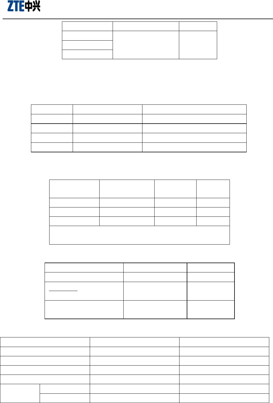
Please refer to table 1-1 for the module’s specification.
Table 1-1 Module’s specification
Models Format Frequency(MHz)
MG3732 WCDMA/HSDPA/GSM/GPRS/EDGE GSM/GPRS/EDGE:
GSM850/EGSM900/DCS1800/PCS1900
WCDMA/HSDPA: 2100M(band I), 1900M
(band II), 850M(band V)
1.1.2 Basic Functions
Please refer to Table 1-2 for the basic functions.
Table 1-2 Basic functions
Item Description
Voice call Circuit-switching service
Packet data Packet data service
SMS Support TEXT
1.1.3 Module’s Interfaces
Please refer to Table 1-3 for the module’s interfaces.
MG3732 module
8
Table 1-3 Interfaces of the modules
1.1.4 Technical parameters
Please refer to Table 1-4 for the module’s technical parameters.
Table 1-4 Technical parameters
Items Descriptions
Working temperature -10°C ~ +50°C
Input voltage 3.3V-4.25V
Maximum current 1800mA @ -102 dBm
Standby current (average) 10mA @ -75 dBm
Call current 230mA @ -75 dBm
Rx. Sensitivity -106.5dBm
Max. Tx power GSM850,EGSM900:33dBm(2W)
GSM1800,PCS1900:30dBm(1W)
WCDMA:23dBm
Frequency range GSM850:
Tx: 824~849 MHz
Rx: 869~894 MHz
EGSM900
Tx: 880~915 MHz
Rx: 925~960MHz
DCS1800
Tx: 1710~1785MHz
Rx: 1805~1880MHz
PCS1900
Tx: 1850~1910MHz
Rx: 1930~1990MHz
WCDMA 2100:
Tx: 1920-1980MHz
Rx: 2110-2170MHz
Interfaces Descriptions
Power interface Supply power to the module, reset the module or turn on/off the module
Audio interface Double audio I/O channel, one for differential, one for single end
USIM interface R-UIM
USB interface USB2.0 High Speed
UART interface Hardware full flow control port, customized by software
PCM interface Transmit voice data for Bluetooth applications
Antenna interface 50 Ohm input resistance control
MG3732 module
9
WCDMA 1900:
Tx: 1850-1910MHz
Rx: 1930-1990MHz
WCDMA 850:
Tx: 824-849MHz
Rx: 869-894MHz
:
1.2.1 Maximum Output Power
Operating
Band
Power Class 1 Power Class 2 Power Class 3 Power Class 4
Power
(dBm)
Tol
(dB)
Power
(dBm)
Tol.
(dB)
Power
(dBm)
Tol
(dB)
Power
(dBm)
Tol
(dB)
Band I +33 +1/-3 +27 +1/-3 +24 +1/-3 +21 +2/-2
Band II - - - - +24 +1/-3 +21 +2/-2
Band V - - - - +24 +1/-3 +21 +2/-2
1.2.2 Frequency Error
Operating Band Frequency Error
Band I <0.1 PPM
Band II <0.1 PPM
Band V <0.1 PPM
1.2.3 Minimum Output Power
Operating Band Minimum Output Power(dBm)
Band I <-50
Band II <-50
Band V <-50
1.2.4 Error Vector Magnitude(EVM)
Parameter Level / Status EVM
Output power 20 dBm
<17.5 % Operating conditions Normal conditions
Power control step size 1 dB
1.2.5 Peak Code Domain Error
Parameter Level / Status Peak Code Domain Error
Output power 20 dBm
<-15dB Operating conditions Normal conditions
Power control step size 1 dB
1.2.6 Occupied Bandwidth
MG3732 module
10
Operating Band Occupied Bandwidth Chip Rate
Band I
<5MHz 3.84Mcps
Band II
Band V
1.2.7 Adjacent Channel Leakage Power Ratio(ALCR)
Power Class UE channel ACLR limit
3 +5 MHz or 5 MHz 33 dB
3 +10 MHz or 10 MHz 43 dB
4 +5 MHz or 5 MHz 33 dB
4 +10 MHz or 10 MHz 43 dB
1.2.1 Reference Sensitivity Level(BER≤0.001)
Operating Band Unit DPCH_Ec
<REFSENS> <REFÎor>
Band I dBm/3.84 MHz -117 -106.7
Band II dBm/3.84 MHz -115 -104.7
Band V dBm/3.84 MHz -115 -104.7
1. For Power class 3 this shall be at the maximum output power
2. For Power class 4 this shall be at the maximum output power
1.2.2 Maximum Input Level(BER≤0.001)
Parameter Level / Status Unit
Îor 25.7 dBm / 3,84MHz
or
c
I
EDPCH _ 19 dB
UE transmitted mean power 20 (for Power class 3 )
18 (for Power class 4) dBm
2.GSM/GPRS/EDGE
Item GSM 850MHz/900MHz GSM 1800MHz/1900MHz
Out Power (GSM) 2W (+33dBm) 1W (+30dBm)
Out Power(EDGE) 500mW (+27dBm) 400mW (+26dBm)
Sensitivity <-102dBm <-102dBm
Frequency Error <0.1 PPM <0.1 PPM
Phane Error Max(°) ≤20 ≤20
RMS(°) ≤5 ≤5
1.2 Relevant Documents
MG3732 module
11
《AT Command Manual for ZTE Corporation's MG3732 Modules》
《Wireless Module Test References》
1.3 Acronyms
A
ADC Analog-Digital Converter
AFC Automatic Frequency Control
AGC Automatic Gain Control
ARFCN Absolute Radio Frequency Channel Number
ARP Antenna Reference Point
ASIC Application Specific Integrated Circuit
B
BER Bit Error Rate
BTS Base Transceiver Station
C
CDMA Code Division Multiple Access
CDG CDMA Development Group
CS Coding Scheme
CSD Circuit Switched Data
CPU Central Processing Unit
D
DAI Digital Audio interface
DAC Digital-to-Analog Converter
DCE Data Communication Equipment
DSP Digital Signal Processor
DTE Data Terminal Equipment
DTMF Dual Tone Multi-Frequency
DTR Data Terminal Ready
E
EFR Enhanced Full Rate
EGSM Enhanced GSM
EMC Electromagnetic Compatibility
EMI Electro Magnetic Interference
ESD Electronic Static Discharge
ETS European Telecommunication Standard
F
FDMA Frequency Division Multiple Access
MG3732 module
12
FR Full Rate
G
GPRS General Packet Radio Service
GSM Global Standard for Mobile Communications
H
HR Half Rate
HSDPA High Speed Downlink Packet Access
I
IC Integrated Circuit
IMEI International Mobile Equipment Identity
ISO International Standards Organization
ITU International Telecommunications Union
L
LCD Liquid Crystal Display
LED Light Emitting Diode
M
MCU Machine Control Unit
MMI Man Machine Interface
MS Mobile Station
P
PCB Printed Circuit Board
PCL Power Control Level
PCS Personal Communication System
PDU Protocol Data Unit
PLL Phase Locked Loop
PPP Point-to-point protocol
R
RAM Random Access Memory
RF Radio Frequency
ROM Read-only Memory
RMS Root Mean Square
RTC Real Time Clock
S
SIM Subscriber Identification Module
SMS Short Message Service
SRAM Static Random Access Memory
MG3732 module
13
T
TA Terminal adapter
TDMA Time Division Multiple Access
TE Terminal Equipment also referred it as DTE
U
UART Universal asynchronous receiver-transmitter
UIM User Identifier Management
UMTS Universal Mobile Telecommunications System
USB Universal Serial Bus
V
VSWR Voltage Standing Wave Ratio
W
WCDMA Wide band Code Division Multiple Access
Z
ZTE ZTE Corporation
MG3732 module
14
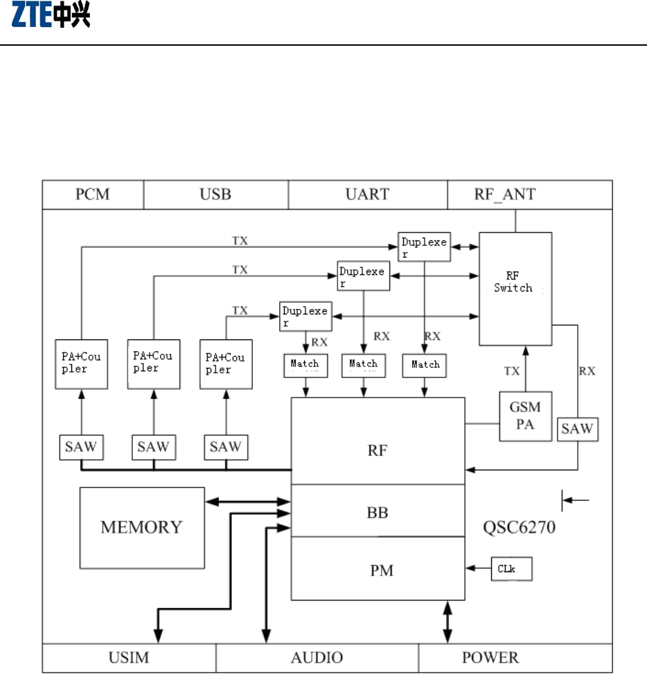
2 Product Introduction
Please refer to Figure 2-1 for the function block diagram of MG3732.
Figure 2-1 MG3732 Function Block Diagram
MG3732 module is WCDMA 3G wireless module developed based on Qualcomm’s QSC6270 platform.
MG3732 module adopts a 36PIN stamp hole, which is applicable for both WCDMA and GSM network. It
supports 850/900/1800/1900/2100 frequency band.
3 PIN Definitions
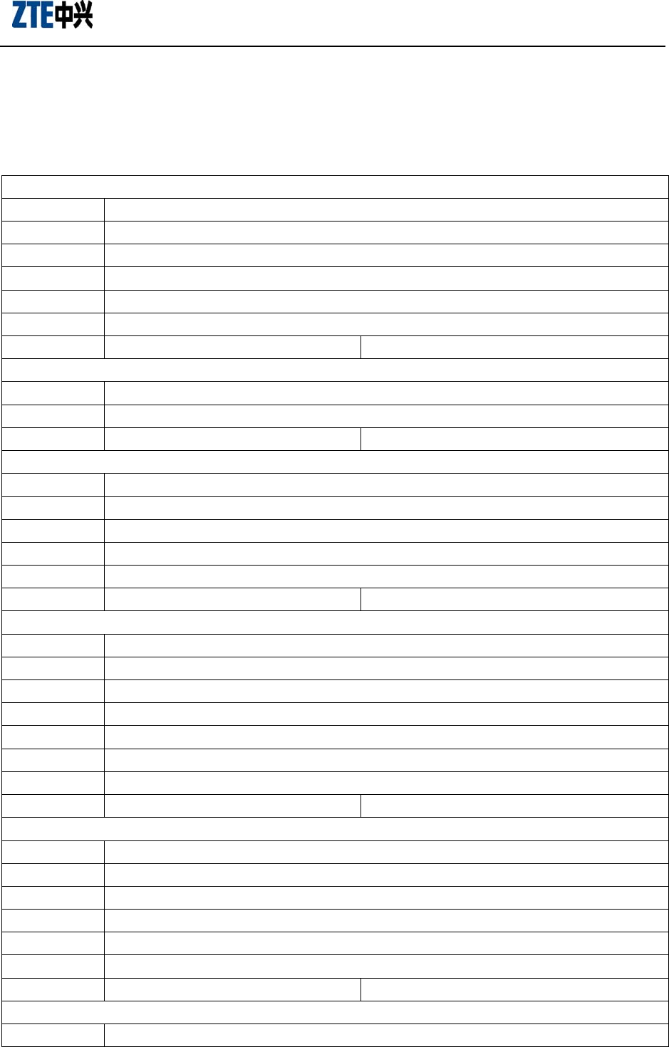
MG3732 module adopts a 36PIN stamp hole and the distance between PINs is 0.5mm. Refer to table 3-1 below
for PIN definitions. Refer to table 3-2 for the key voltage of each pin.
MG3732 module
15
Table 3-1 PIN definitions
1 VREG_USIM
UIM
MG3732MD_A
GND 36
2 USIM_RST
GND 35
3 USIM_CLK
LED
SIG_LED 34
4 USIM_DATA
PCM
PCM_DIN 33
5 GND
PCM_CLK 32
6 EAR2_P
AUDIO
USB
USB_DM 31
7 EAR1_P USB_DP 30
8 EAR1_N
ON/OFF 29
9 MIC2_P
UART
PCM_SYNC(/DS
R) 28
10 MIC1_P PCM_DOUT(DC
D) 27
11 MIC1_N /DTR 26
12 GND
/RTS 25
13 /PON_RESET
RI 24
14 VBUS
POWER
TXD 23
15 VCHG RXD 22
16 V_MAIN /CTS 21
17 V_MSME_1V8
GND 20
18 V_MAIN
ANT
RF_ANT 19
Refer to table 3-1 below for PIN definitions of MG3732 module.
Table 3-2 PIN definitions
Function Pin No. Signal name I/O Basic functions Remarks
SIM card
interface
1 VREG_USIM O 2.85V/1.8V
2 USIM_RST O USIM card reset signal
3 USIM_CLK O USIM card clock
4 USIM_DATA I/O USIM card data cable
Audio
6 EAR2_P O Single-end audio output
channel 2
7 EAR1_P O Differential audio output
channel 1, anode
8 EAR1_N O Differential audio output
channel 1, cathode
9 MIC2_P I Single-end audio input
channel 2
10 MIC1_P I Differential audio input
channel 1, anode
11 MIC1_N I Differential audio input
channel 1, cathode
MG3732 module
16
Reset 13 /PON_RESET I Reset signal Low level valid
Power
14 VBUS I USB power +5V
15 VCHG I Charge power
16 V_MAIN I Module’s main power 3.3V-4.2V
17 V_MSME_1V8 O Digital power Voltage output, 1.8V
18 V_MAIN I Module’s main power 3.3V-4.2V
29 ON/OFF I Power on/off control 1.8V, Low level valid
UART
21 /CTS I Clear to send 1.8V, Low level valid
22 RXD I Receive data 1.8V
23 TXD O Transmit data 1.8V
24 RI O Ring tone 1.8V
25 RTS O Request to send 1.8V, Low level valid
26 /DTR I Data terminal ready 1.8V, Low level valid
PCM
27 PCM_DOUT
(DCD) O PCM data output 1.8V, duplex with DCD
28 PCM_SYNC
(/DSR) O PCM frame SYNC clock 1.8V, duplex with
/DSR
32 PCM_CLK O PCM data clock 1.8V
33 PCM_DIN I PCM data input 1.8V
USB
interface
30 USB_DP I/O USB data+
31 USB_DM I/O USB data-
LED 34
SIG_LED O Module’s working status
LED
Antenna 19 RF_ANT I/O Antenna interface
GND
5、12、
20、35、
36
GND
4 Decription of Hardware Interfaces
4.1 Summary
MG3732 module
17
This chapter introduces each logic function interfaces of MG3732 module & its operation descriptions, and
provides the designing sample.
Power and Reset Interface
COM Port
UIM Card Interface
Audio Interface
PCM interface
USB2.0 interface
Antenna Interface
Remarks: In the system, the module layout should be far away from high-speed circuit, switch power, power
transformer, large power inductor, or single chip microcomputer’s clock circuit.
4.2 Power and Reset
4.2.1 Power Design
The module could work under two power modes: 1. Power adaptor; 2. Battery
The power could directly be supplied externally, the external power is added directly to V_MAIN and meets
the voltage requirements in table 4-1. The external power could be supplied by the power adaptor with constant
output, battery, USB power converter, etc. It’s recommended to design 2A current to meet the requirements of
GSM/GPRS.
Table 4-1 Voltage characteristics
Classification MIN. Typical Max.
Input voltage 3.3 V 3.8 V 4.25 V
Power on
The module will be turned off after power-on normally. To turn on the module, provide a 2000-2500mS
low level pulse to ON/OFF PIN.
Power off
To turn off the module, provide a 2500-4000mS low level pulse to ON/OFF PIN.
Reset
To reset the module, provide a 2500-4000mS low level pulse to ON/OFF PIN
After reset, the module will be turned off. To turn on the module, provide a 2000-2500mS low level
pulse to ON/OFF PIN.
V_MSME_1V8
There is a voltage output pin with current adjuster on MG3732 module, which can be used to supply external
power to the board. The voltage of this pin and the voltage of baseband processor/memory come from the same
voltage adjuster. The voltage output is available only when the module is on. The normal output voltage is 1.8V,
and the user should absorb the current from this pin as little as possible (less than 10mA). Generally, it is
recommended to use this pin for pull-up when matching the level.
MG3732 module
18
Other Advice
In order to make sure the data is saved safely, please don’t cut off the power when the module is on. It’s
strongly recommended to use ON/OFF pin or AT command to turn off the mobile phone.
4.3 COM Port
The module provides a full duplex UART interface, whose maximal data rate is 230.4kbps and typical data rate
is 11.5kbps. External interface is 1.8VCMOS level signal, which could be used for upgrade, port
communication, etc.
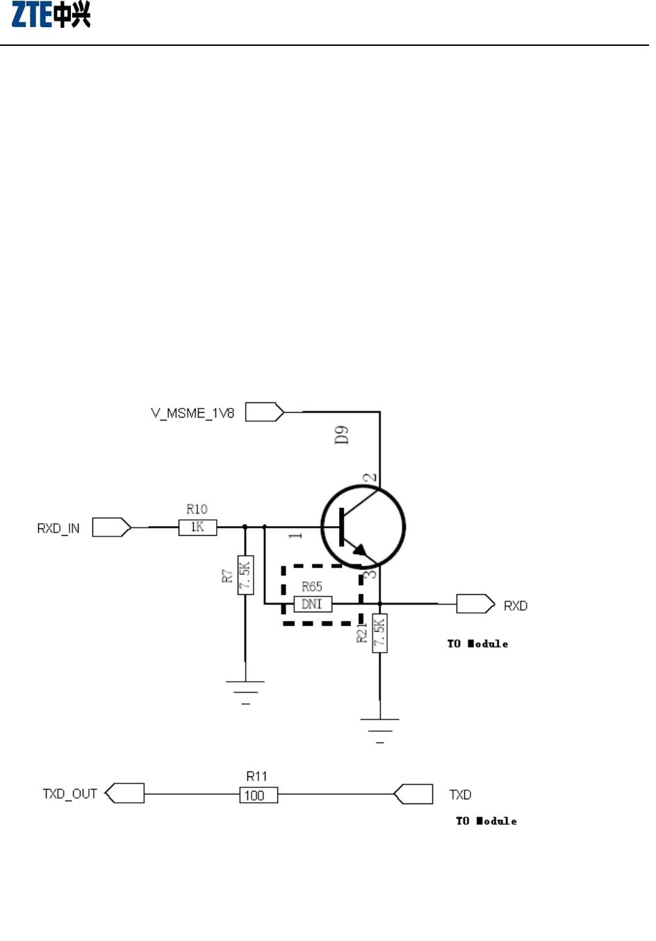
When using MG3732 module’s UART port to communicate with PC or MCU, please pay attention to the
direction of TX, RX. It’s specially noted that MG3732 module’s UART port only supports 1.8V, therefore for
non 1.8V external UART, it needs to convert the level. Normally a dynatron is used to realize the level
conversion. As shown in figure 4-1, the resistance is just for your information, please calculate again during the
design.
Figure 4-1 UART Interface Reference Design Diagram
4.4 UIM Card Interface
MG3732 module
19
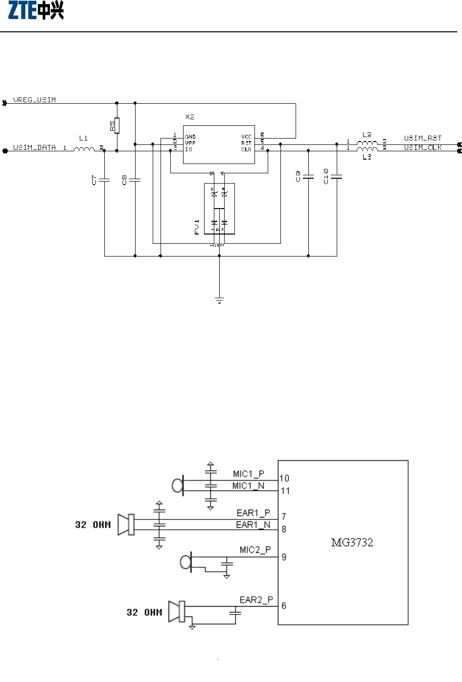
The module supports 2.85V/1.8V UIM card, and it’s strongly recommended to add ESD component to protect
UIM card as shown in figure 4-2.
Figure 4-2 UIM Card Circuit Reference Design Diagram
Note: The clock data rate of UIM card circuit is 4M, and the card socket should be laid closely around the
module and the wiring should be as short and thick as possible.
4.5 Audio Interface
The module provides 2 speaker interfaces and 2 microphone interfaces. Only one pair I/O works at the same
time. See the audio interface circuit in figure 4-3.
Figure 4-3 Audio Interface Circuit Reference Design Diagram
Microphone
The two microphone interfaces MIC_N and MIC_P are differential interface, which could also be used for
single end input. It’s recommended to use differential mode to reduce the noises and it is directly connected with

MG3732 module
20
the receiver. MIC_P is single ended interface, which could be directly connected to the microphone since the
offset voltage is internally provided.
Earpiece
The earpiece interface EAR1_P and EAR1_N are both differential interfaces with 32Ω resistance; EAR2_P is
single-ended interface with 32Ω resistance and no coupling of capacitor is required.
Design of audio interface on the receiver
Select the microphone with the sensitivity lower than -52dB since EAR1’s output power is 35mW and the max.
gain inside MIC1 reaches 52dB.
Note: if other kind of audio input method is adopted, the input signal should be within 1V. If the signal
voltage is lower than 1V, then the pre-amplifier should be added. If the signal voltage is higher than 1V,
then network attenuation should be added
Design of audio interface on the earpiece
Select the microphone with the sensitivity lower than -52dB since EAR2’s output power is 10.8mW and the
max. gain inside MIC2 reaches 52dB. The level of MIC2_P PIN is about 1.8V. The receiver’s design is just the
same as the receiver’s.
4.6 PCM Interface
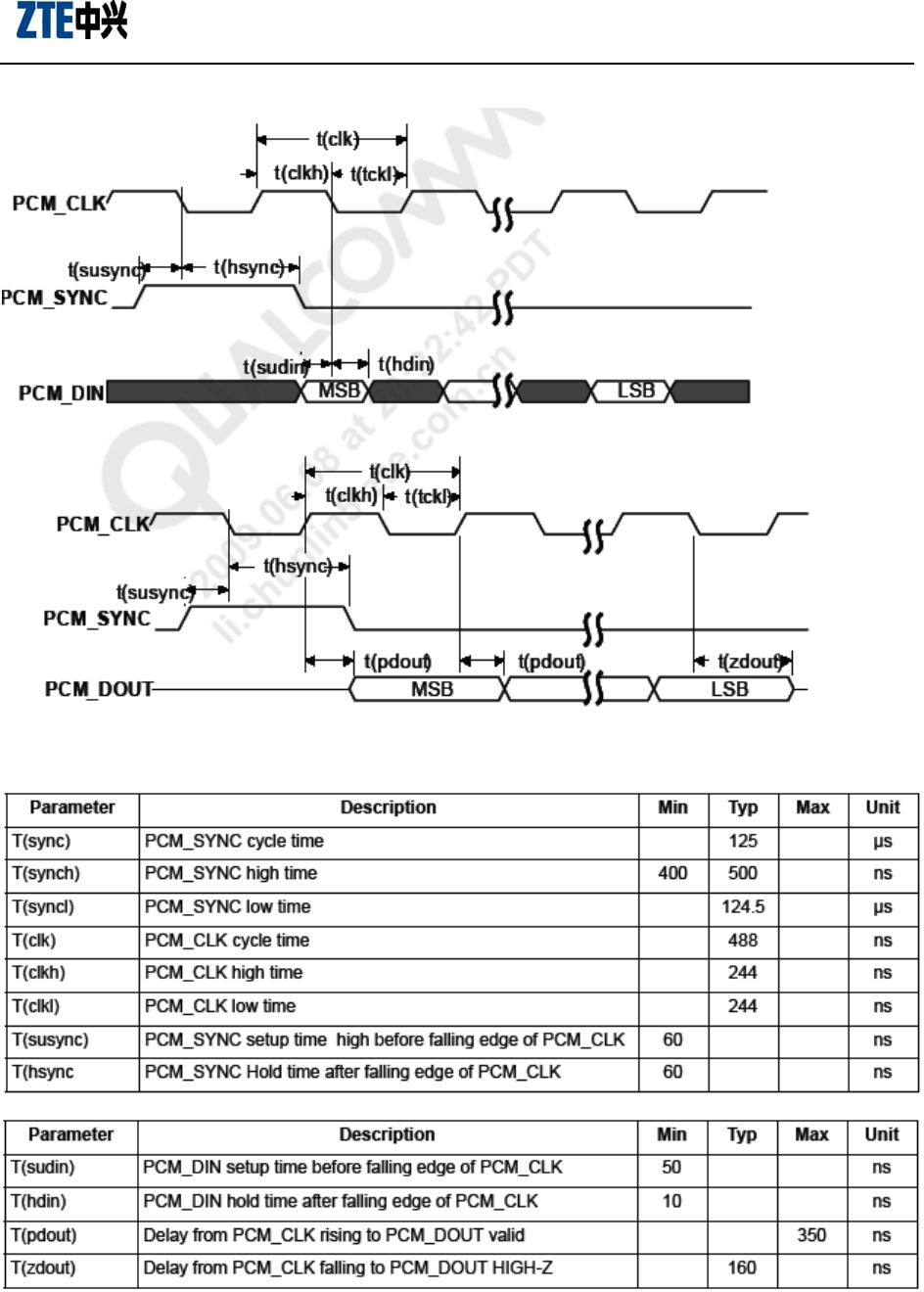
The module’s PCM interface provides PCM_CLK, PCM_SYNC, PCM_DIN, PCM_DOUT,and it supports
2.048MHz PCM clock data rate and 8K frame data rate. PCM clock will stop the output when it enters the
dormant mode.
The module’s PCM interface must work under Master mode, and the clock and SYNC signal must be sent by
the module. The device connected with the interface can word under Slave mode only.
See the time sequence of PCM interface in figure 4-4.
MG3732 module
21
Figure 4-4 Time Sequence of PCM Interface
4.7 USB2.0 Interface
The module provides USB2.0 HS interface with 480Mbps, which is composed of VBUS, D+ and D-. You can
directly connect USB signal interface when designing the module’s external circuit, but try to add ESD
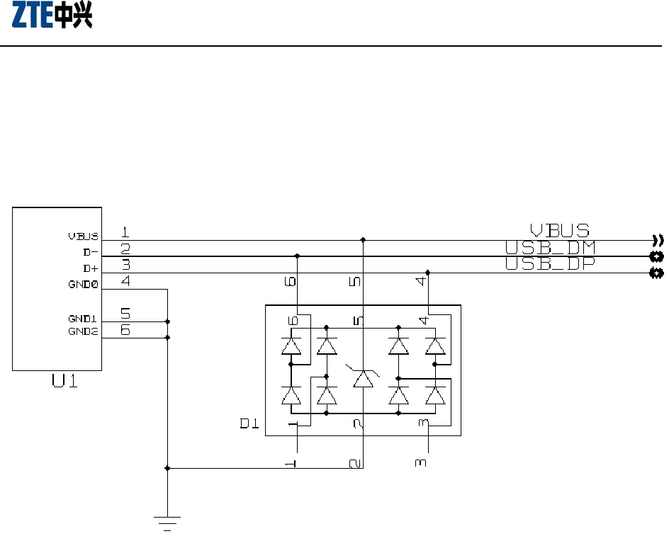
MG3732 module
22
protector during the design to avoid damaging the module.
D1 is USB2.0 ESD protector in the figure, and the Junction capacitance is small than 3P. VBUS is connected to
the external host VBUS. The USB operating voltage is: 4.75—5.25V with the typical value of 5V. See figure
4-5.
Figure 4-5 USB Interface Circuit Reference Design Diagram
4.8 Antenna Interface
Proper measures should be taken to reduce the access loss of effective bands, and good shielding should be
established between the external antenna and the RF connector. Besides, the external RF cables should be kept
far away from all interference sources such as high-speed digital signal or switch power supply.
According to mobile station standard, stationary wave ratio of antenna should be between1.1 to 1.5, and input
impedance is 50 ohm. Different environments may have different requirements on the antenna’s gain. Generally,
the larger gain in the band and smaller outside the band, the better performance the antenna has. Isolation
degree among ports must more than 30dB when multi-ports antenna is used. For example, between two
different polarized ports on dual-polarized antenna, two different frequency ports on dual-frequency antenna, or
among four ports on dual-polarized dual-frequency antenna, isolation degree should be more than 30dB.
MG3732 module
23
5 Mechanical Design
5.1 Appearance Diagram
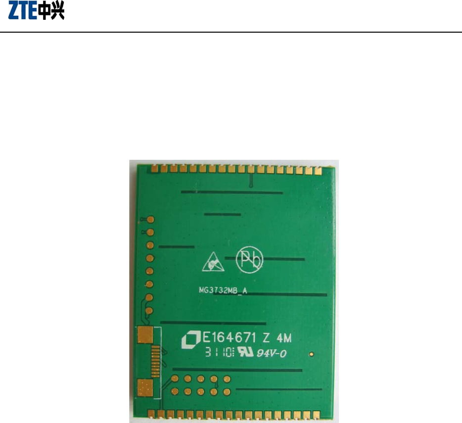
See the appearance of MG3732 module in figure 5-1.
Figure 5-1 MG3732 Module’s Appearance
Dimensions:(LxWxH):39.5 mm x 31.0mm x2.65mm
Weight: 7g
MG3732 module
24
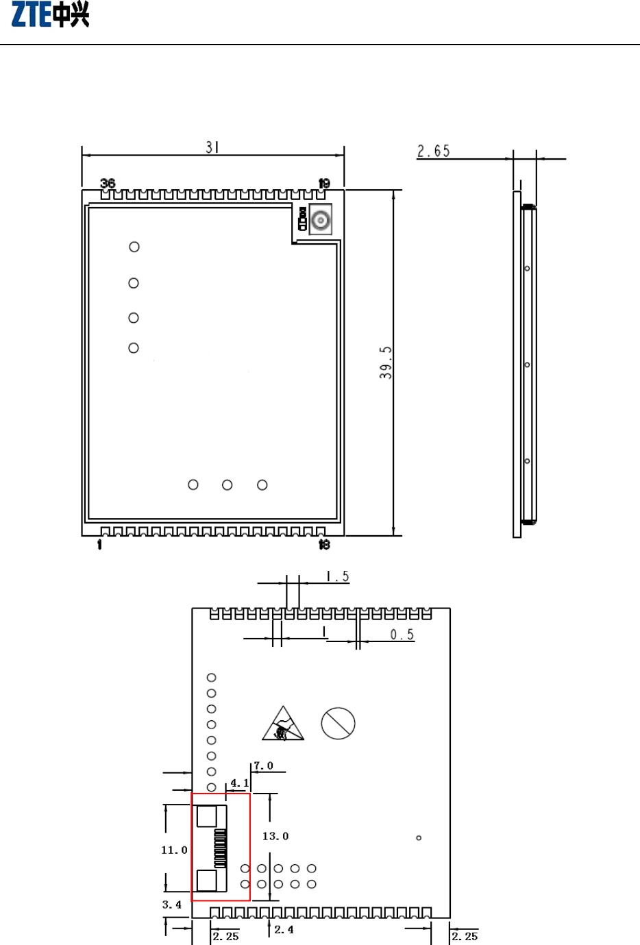
5.2 Module Assembly Diagram
See the assembly diagram of MG3732 module in figure 5-2.
Figure 5-2 Module’s Assembly Diagram
Note: it’s recommended to open a window in the relevant position of the red area on the bottom layer for the
convenience of maintenance. The red box is made manually and doesn’t exist on the actual object. See the
dimensions for the hole in the figure above.

MG3732 module
25
5.3 Module’s Fixing Method
The module’s fastening method adopts direct manual soldering to avoid second-time soldering. It’s strongly
recommend to use the manual soldering because MC3732 module board is just 0.8mm thick and QSC6270
BGA space is too small. The second-time soldering would cause the melting of soldering tin and lead to short
circuit of QSC6270 main chip, such as USB disconnected, large current, etc.
FCC Regulations:
This device complies with part 15 of the FCC Rules. Operation is subject to the following two conditions: (1)
This device may not cause harmful interference, and (2) this device must accept any interference received,
including interference that may cause undesired operation.
This device has been tested and found to comply with the limits for a Class B digital device, pursuant to Part
15 of the FCC Rules. These limits are designed to provide reasonable protection against harmful interference in
a residential installation. This equipment generates, uses and can radiated radio frequency energy and, if not
installed and used in accordance with the instructions, may cause harmful interference to radio communications.
However, there is no guarantee that interference will not occur in a particular installation If this equipment does
cause harmful interference to radio or television reception, which can be determined by turning the equipment
off and on, the user is encouraged to try to correct the interference by one or more of the following measures:
-Reorient or relocate the receiving antenna.
-Increase the separation between the equipment and receiver.
-Connect the equipment into an outlet on a circuit different from that to which the receiver is connected.
-Consult the dealer or an experienced radio/TV technician for help.
Changes or modifications not expressly approved by the party responsible for compliance could void the user‘s
authority to operate the equipment.
RF Exposure Information
This Modular Approval is limited to OEM installation for mobile and fixed applications only. The antenna
installation and operating configurations of this transmitter, including any applicable source-based
time-averaging duty factor, antenna gain and cable loss must satisfy MPE categorical Exclusion Requirements
of §2.1091.
The antenna(s) used for this transmitter must be installed to provide a separation distance of at least 20 cm from
all persons, must not be collocated or operating in conjunction with any other antenna or transmitter, except in
accordance with FCC multi-transmitter product procedures.
The end user has no manual instructions to remove or install the device and a separate approval is required for

MG3732 module
26
all other operating configurations, including portable configurations with respect to 2.1093 and different
antenna configurations.
Maximum antenna gain allowed for use with this device is 2 dBi.
When the module is installed in the host device, the FCC ID label must be visible through a window on the
final device or it must be visible when an access panel, door or cover is easily re-moved. If not, a second label
must be placed on the outside of the final device that contains the following text: “Contains FCC ID:
Q78-MG3732.
.