ZTE MW3736 WCDMA wireless data terminal User Manual user guide
ZTE Corporation WCDMA wireless data terminal user guide
ZTE >
User Manual

ZTEMW3736Hardware
Design
UserManual
Intend to OEM Integrator Installation
Version:V1.0

Intend to OEM Integrator Installation
It’s not allowed to spread without the
permission of ZTE Corporation. © ZTE Corporation. All rights reserved. 第I页
CopyrightStatement
IfyouacceptthismanualofZTECorporation,itmeansthatyouhaveagreedtothefollowingterms
andconditions;ifyoudon’tagree,pleasestopusingthismanual.
ThecopyrightofthismanualbelongstoZTECorporation.ZTECorporationreservesanyrightsnot
expresslygrantedinthismanual.Thecontentsinthismanualaretheproprietaryinformationof
ZTECorporation.Thismanualandanyimage,table,dataorotherinformationcontainedinthis
manualmaynotbereproduced,transferred,distributedutilizedordisclosedwithouttheprior
writtenpermissionofZTECorporation.
and aretheregisteredtrademarkofZTECorporation.Allothertrademarks
appearedinthismanualareownedbytherelevantcompanies.Nothingcontainedinthismanual
shouldbeconstruedasgranting,byimplication,estoppel,orotherwise,anylicenseorrighttouse
anytrademarksdisplayedinthismanualwithoutthepriorwrittenpermissionofZTECorporation
orthird‐partyobligee.
Thisproductconformstothedesignrequirementsofrelevantenvironmentprotectionand
personalsafety.Thestorage,usageanddisposalofthisproductshouldcomplywiththeproduct
usermanual,relevantcontractsorrequirementsoflawsandregulationinrelevantcountries.
ZTECorporationkeepstherighttomodifyorimprovetheproductdescribedinthemanualwithout
priornotice;andmeanwhilekeepstherighttomodifyorretractthismanual.
Ifthereisanythingambiguousinthismanual,pleaseconsultZTECorporationoritsdistributoror
agentpromptly.
Intend to OEM Integrator Installation
第II 页 © ZTE Corporation. All rights reserved. It’s not allowed to spread without the
permission of ZTE Corporation
Versionupdatedescription
Productversion Documentversion DocumentNo. Documentupdatedescriptions
V1.0 Releasedforthefirsttime
Writer
Documentversion Date Writtenb
y
Requestedb
y
Approvedb
y
V1.0 2012‐08‐07LiuChangdi
YuXianwu

Intend to OEM Integrator Installation
It’s not allowed to spread without the
permission of ZTE Corporation. © ZTE Corporation. All rights reserved. 第III 页
Important compliance information for North American users
The MW3736 Module has been granted modular approval for mobile applications. Integrators may use the
MW3736 Module in their final products without additional FCC certification if they meet the following
conditions. Otherwise, additional FCC approvals must be obtained.
1. At least 20cm separation distance between the antenna and the user’s body must be maintained at all
times.
2. To comply with FCC regulations limiting both maximum RF output power and human exposure to RF
radiation, the maximum antenna gain including cable loss in a mobile-only exposure condition must not
exceed 3dBi in the GSM850/WCDMA850 band and 5dBi for GSM1900/WCDMA1900 band.
3. The MW3736 Module and its antenna must not be co-located or operating in conjunction with any
other transmitter or antenna within a host device. This equipment complies with FCC RF radiation
exposure limits set forth for an uncontrolled environment.
4. A label must be affixed to the outside of the end product into which the MW3736 Module is
incorporated, with a statement similar to the following: For MW3736: This device contains FCC ID:
Q78-MW3736.
5. A user manual with the end product must clearly indicate the operating requirements and conditions
that must be observed to ensure compliance with current FCC RF exposure guidelines.
The end product with an embedded MW3736 Module may also need to pass the FCC Part 15 unintentional
emission testing requirements and be properly authorized per FCC Part 15.
Note: If this module is intended for use in a portable device, you are responsible for separate
approval to satisfy the SAR requirements of FCC Part 2.1093.
FCC NOTICE:
This device complies with Part 15 of the FCC Rules.
Operation is subject to the following two conditions:
(1) this device may not cause harmful interference, and
(2) this device must accept any interference received, including interference that may cause undesired
operation.
Changes or modifications made to this equipment not expressly approved by ZTE Corporation may void the
FCC authorization to operate this equipment.

Intend to OEM Integrator Installation
第IV 页 © ZTE Corporation. All rights reserved. It’s not allowed to spread without the
permission of ZTE Corporation
Withstrongtechnicalforce,ZTECorporationcanprovideCDMA/GPRS/WCDMA/GSMmodule
customerswiththefollowingall‐aroundtechnicalsupport:
1.Providecompletetechnicaldocumentation;
2.ProvidethedevelopmentboardusedforR&D,test,production,after‐sales,etc.
3.Provideevaluationsandtechnicaldiagnosisforprinciplediagram,PCB,testscenarios;
4.Providetestenvironment;
ZTECorporationprovidescustomerswithonsitesupports,andalsoyoucouldgetsupportsthrough
telephone,website,instantmessenger,E‐mail,etc.

Intend to OEM Integrator Installation
It’s not allowed to spread without the
permission of ZTE Corporation. © ZTE Corporation. All rights reserved. 第V页
Preface
Summary
ThisusermanualmainlydescribesZTEMW3736module’sproductprinciplediagram,module’sPINs,
hardwareinterfacesandmodulestructure.Thismanualisusedtoinstructtheusersonthemodule’s
hardwaredesign,andonthebasisofthismodule,quicklyandconvenientlydesigndifferentkindsof
wirelessterminals.
TargetReaders
Systemdesigningengineers
Mechanicalengineers
Hardwareengineers
Softwareengineers
Testingengineers
Descriptionofcontents:
Thismanualcontains5chapters.Seethetablebelow:
1.Module’sGeneraldescription.ThischapterintroducesMW3736module’sbasictechnical
specification,relevantdocumentsandabbreviations.
2.Module’sExternalInterfaces.ThischapterintroducesMW3736module’spinnameandfunctions.
3.Module’sElectricalCharacteristics.ThischapterdescribesMW3736module’sinterfacelevel,
powerconsumption,reliability,etc.
4.DescriptionofHardwareInterfaces.ThischapterdescribesMW3736’shardwareinterfaces.
5.MechanicalDesign.ThischapterdescribesMW3736module’sappearancediagram,assembly
diagramandPCBlayoutonthemainboard.

Intend to OEM Integrator Installation
第VI 页 © ZTE Corporation. All rights reserved. It’s not allowed to spread without the
permission of ZTE Corporation
Contents
1MODULE’S GENERAL DESCRIPTION .......................................................................... 1
1.1INTRODUCTION TO MODULE’S FUNCTIONS ..................................................... 1
1.2MODULE’S PRINCIPLE BLOCK DIAGRAM .......................................................... 2
1.3ABBREVIATIONS ................................................................................................... 3
2DESCRIPTION OF MODULE’S EXTERNAL INTERFACES ........................................... 6
2.1DEFINITIONS OF MODULE’S INTERFACES ........................................................ 6
2.2ANTENNA INTERFACE ......................................................................................... 8
2.3ANTENNA INTERFACE’S RF PERFORMANCE ................................................... 9
3MODULE’S ELECTRICAL CHARACTERISTICS ......................................................... 10
3.1DESCRIPTIONS OF INTERFACE LEVEL ........................................................... 10
3.2POWER ON/OFF TIME SEQUENCE ................................................................... 10
3.3RELIABILITY ........................................................................................................ 11
3.4ESD ...................................................................................................................... 11
4REFERENCE DESIGN OF INTERFACE CIRCUITS ..................................................... 13
4.1POWER AND RESET .......................................................................................... 13
4.2COM PORT .......................................................................................................... 14
4.3UIM CARD INTERFACE ....................................................................................... 17
4.4AUDIO INTERFACE (OPTIONAL) ....................................................................... 18
4.5WORK STATUS INDICATORS ............................................................................ 19
5MECHANICAL DESIGN ................................................................................................ 20
5.1APPEARANCE DIAGRAM ................................................................................... 20
5.2MODULE’S ASSEMBLY DIAGRAM ..................................................................... 21
5.3MODULE’S PCB ENCAPSULATION DIMENSIONS ............................................ 22
Intend to OEM Integrator Installation
It’s not allowed to spread without the
permission of ZTE Corporation. © ZTE Corporation. All rights reserved. 第1页
1 Module’sGeneralDescription
With36‐PINstamp‐hole interface,MW3736moduledevelopedbyZTECorporationisakindof
WCDMA/GSMindustrialmodule,whichcanbebuiltintheSet‐Top‐Box,vehicle‐mountedterminals,
andenable users to getaccess to theInternet wirelessly andsend/receive Emails, browse the web
pages,downloadathighspeedandplayonlinevideos,etc.
ItenablesuserstogetaccesstotheInternetanytimeinaplace where WCDMA/GSM network is
covered.ItalsofeaturesinSMS,voicecall,etc.andprovideshighlyfreeandconvenientsolutionsfor
usersinmobiledatacommunication,andtrulyrealizesthedreamofmobileoffice.
MW3736moduleisdividedintotwoproductswithdifferentfrequencybands,respectivelynamed
as MW3736_V1A and MW3736_V1B. They can be recognized through the silkscreen printed at the
bottom of it. MW3736_V1A corresponds to the frequency band WCDMA850/1900,
GSM850/900/1800/1900; while MW3736_V1B corresponds to the frequency band
WCDMA850/900/2100,GSM850/900/1800/1900.
Thischaptermainlyintroducesthemodule’sbasicfunctionsandlogicblockdiagrams.
1.1 IntroductiontoModule’sFunctions
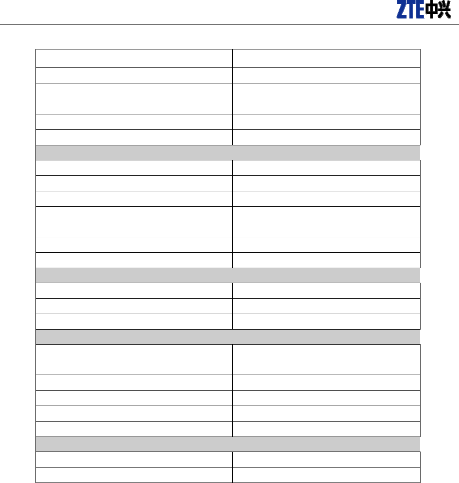
Table1‐1 Module’sfunctions
ParametersMW3736
Basicfeatures
Frequencyband WCDMA850/1900、
GSM850/900/1800/1900
Dimensions 39.50mm×31.00mm×2.65mm
Weight 10g
Worktemperature ‐25℃~+65℃
Storagetemperature ‐30℃~+85℃
Performance
Workvoltage 3.6V~4.2V
Standard:3.8V
Standardconsumption
Sleepcurrent(Min.):1mA
Idlecurrent(Ave.):5mA@‐75dBm
Talkcurrent:230mA@‐75dBm
Maximumcurrent(instantaneousvalue):
1800mA@‐102dBm
Maximumoutputpower 21dBm~32.5dBm@‐102dBm
Rx.signalsensitivity ‐108dBm
Interface
Intend to OEM Integrator Installation
第2页 © ZTE Corporation. All rights
reserved. It’s not allowed to spread without the
permission of ZTE Corporation
ParametersMW3736
Connectionmethod 36Pinstamp‐hole
Antenna U.FL‐R‐SMT50ohmantennaconnector
Integratedfullduplexport ATcommand,datatransmission
UIMcardsocketlevel 1.8V/2.85V
Dataservice
Mode WCDMA/GSM/EDGE
Max.downlinkdatarate 14.4Mbps
Max.uplinkdatarate 5.76Mbps
ProtocolInternalTCP/IPandUDP/IPprotocolstack
TCPserver
EmbeddedFTP
SMS
SupportTEXT/PDUmode
PTPMO/MT
SMSCellBroadcast
Audio(optional)
PCMaudio
Headset
AudioencoderEVRC&13KQCELP
Volumecontrol
SupportDTMF
ATcommandsettings
CommonATcommands
ZTEexclusiveATcommands
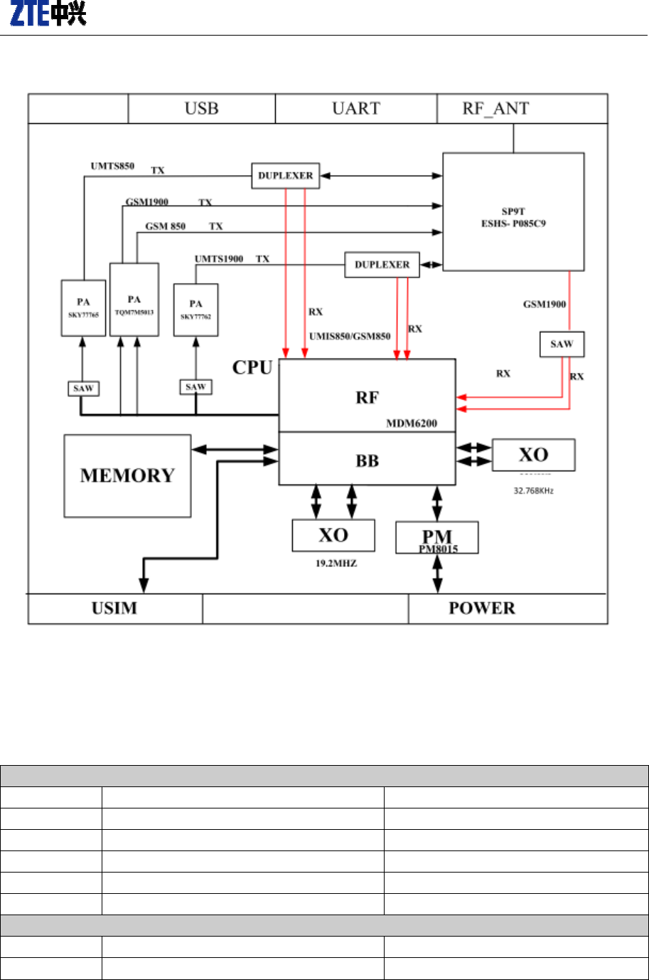
1.2 Module’sPrincipleBlockDiagram
SeeMW3736’smajorlogicfunctionsinthefollowingblockdiagram:
Figure1‐1Module’sprinciplediagram
Intend to OEM Integrator Installation
It’s not allowed to spread without the
permission of ZTE Corporation. © ZTE Corporation. All rights reserved. 第3页
MW3736_principlediagram:
1.3 Abbreviations
Table1‐2IntroductiontoAbbreviations
A
ADC Analog‐DigitalConverter
AFC AutomaticFrequencyControl
AGC AutomaticGainControl
ARFCN AbsoluteRadioFrequencyChannelNumber
ARP AntennaReferencePoint
ASIC ApplicationSpecificIntegratedCircuit
B
BER BitErrorRate
BTS BaseTransceiverStation
Intend to OEM Integrator Installation
第4页 © ZTE Corporation. All rights
reserved. It’s not allowed to spread without the
permission of ZTE Corporation
C
CDMA CodeDivisionMultipleAccess
CDG CDMADevelopmentGroup
CS CodingScheme
CSD CircuitSwitchedData
CPU CentralProcessingUnit
D
DAI DigitalAudiointerface
DAC Digital‐to‐AnalogConverter
DCE DataCommunicationEquipment
DSP DigitalSignalProcessor
DTE DataTerminalEquipment
DTMF DualToneMulti‐Frequency
DTR DataTerminalReady
E
EFR EnhancedFullRate
EGSM EnhancedGSM
EMC ElectromagneticCompatibility
EMI ElectroMagneticInterference
ESD ElectronicStaticDischarge
ETS EuropeanTelecommunicationStandard
F
FDMA FrequencyDivisionMultipleAccess
FR FullRate
G
GPRS GeneralPacketRadioService
GSM GlobalStandardforMobileCommunications
H
HR HalfRate
I
IC IntegratedCircuit
IMEI InternationalMobileEquipmentIdentity
ISO InternationalStandardsOrganization
ITU InternationalTelecommunicationsUnion
L
LCD LiquidCrystalDisplay
LED LightEmittingDiode
M
MCU MachineControlUnit
MMI ManMachineInterface
MS MobileStation
P
PCB PrintedCircuitBoard
Intend to OEM Integrator Installation
It’s not allowed to spread without the
permission of ZTE Corporation. © ZTE Corporation. All rights reserved. 第5页
PCL PowerControlLevel
PCS PersonalCommunicationSystem
PDU ProtocolDataUnit
PLL PhaseLockedLoop
PPP Point‐to‐pointprotocol
R
RAM RandomAccessMemory
RF RadioFrequency
ROM Read‐onlyMemory
RMS RootMeanSquare
RTC RealTimeClock
S
SIM SubscriberIdentificationModule
SMS ShortMessageService
SRAM StaticRandomAccessMemory
T
TA Terminaladapter
TDMA TimeDivisionMultipleAccess
TE TerminalEquipmentalsoreferreditasDTE
U
UART Universalasynchronousreceiver‐transmitter
UIM UserIdentifierManagement
USB UniversalSerialBus
V
VSWR VoltageStandingWave Rati o
Z
ZTE ZTECorporation
Intend to OEM Integrator Installation
第6页 © ZTE Corporation. All rights
reserved. It’s not allowed to spread without the
permission of ZTE Corporation
2 DescriptionofModule’sExternalInterfaces
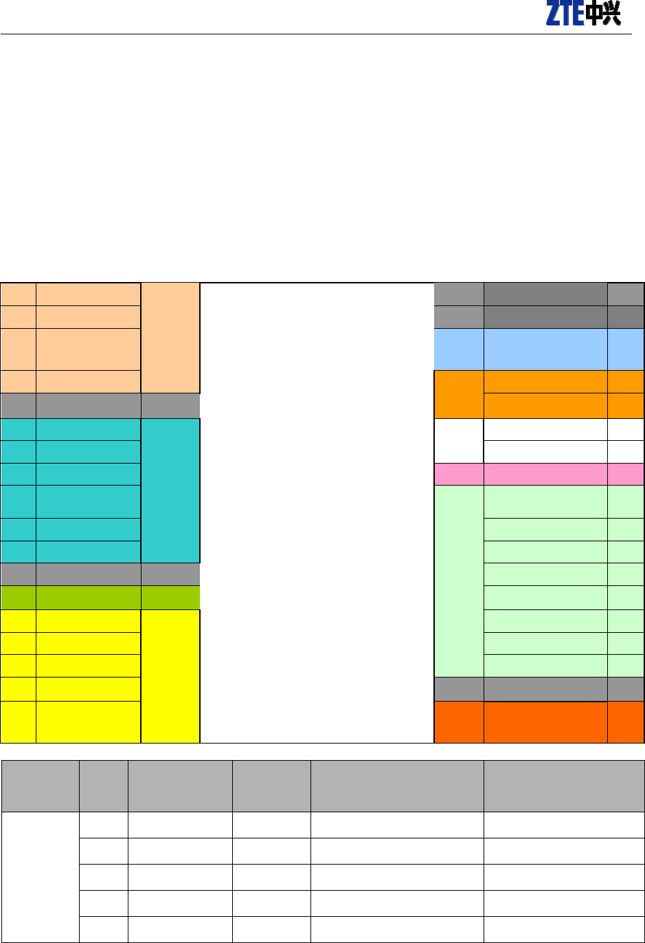
MW3736moduleadopts36pinstamp‐holeinterfacetoconnectexternally.
2.1 DefinitionsofModule’sInterfaces
Table2‐1Definitionsofmodule’sinterface
1VREG_USIM
UIM
MW3736
GND36
2USIM_RST
GND35
3USIM_CLK
LED
SIG_LED34
4USIM_DATA
PCM
(Opti
onal
)
PCM_DIN33
5GND
PCM_CLK32
6NC
USB
USB_DM31
7NCUSB_DP30
8NC
ON/OFF29
9NC
UART
PCM_SYNC(/DS
R
)28
10
NCPCM_DOUT(DCD)
27
11
NC/DTR26
12
GND
/RTS25
13
/PON_RESET
RI24
14
VBUS
POWER
TXD23
15
NCRXD22
16
VBAT/CTS21
17
V_MSME_1V8
GND20
18
VBAT
ANT
RF_ANT19
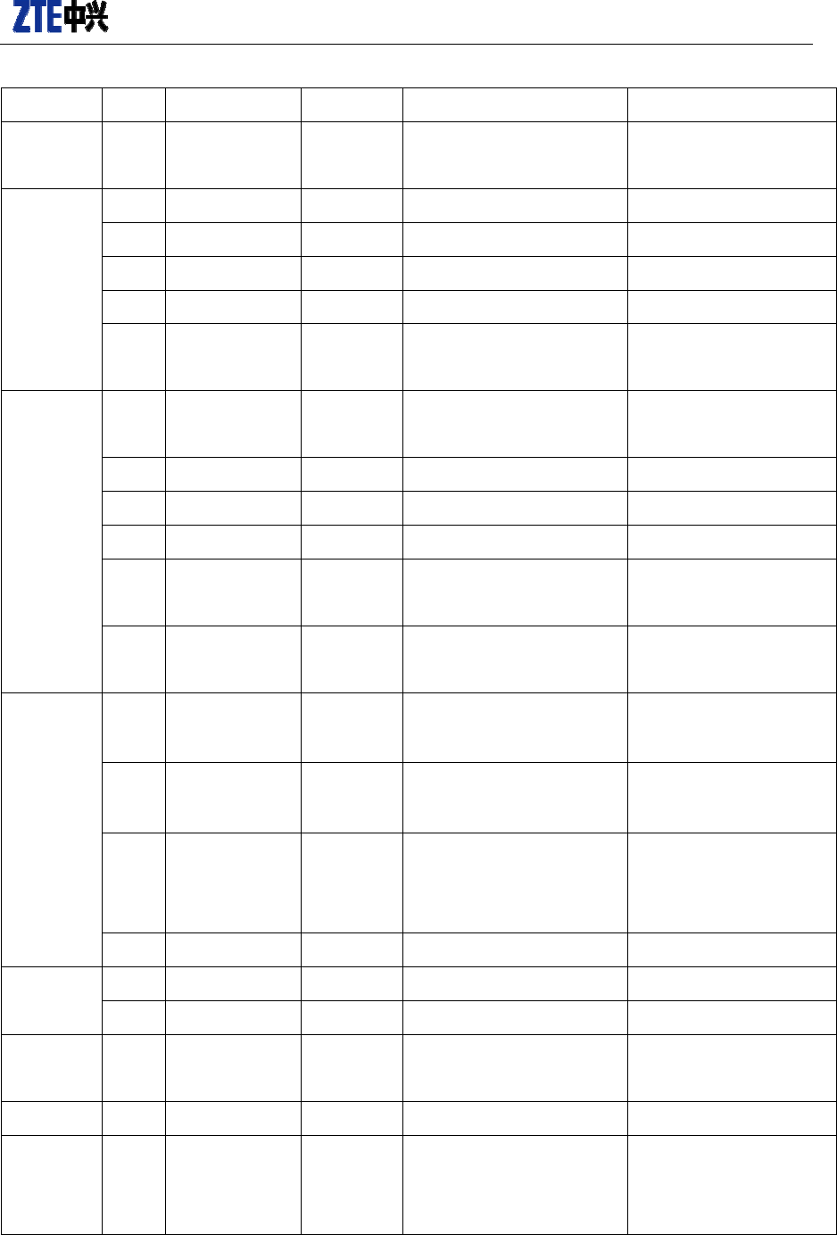
Functions Pin
No.
Signalname I/O Basicfunctions Remarks
SIMcard
interface
1 VREG_USIM O 2.85V/1.8Vpowersupply
2 USIM_RST O USIM cardresetsignal
3 USIM_CL
K
O USIM cardclockcable
4 USIM_DATA I/O USIM carddatacable
11 MIC1_N I Differential audio input
Intend to OEM Integrator Installation
It’s not allowed to spread without the
permission of ZTE Corporation. © ZTE Corporation. All rights reserved. 第7页
channel1‐
Reset 13 /PON_RESET I Resetsignal 1.8V, valid upon low
le ve l
Power
14 VBUS I USB power +5V
16 VBAT I Module’smainpower 3.3V‐4.2V
17 V_MSME_1V8 O Digitalpower Voltageoutput, 1.8V
18 VBAT I Module’smainpower 3.3V‐4.2V
29 ON/OFF I Poweron/offcontrol 1.8V, valid upon low
le ve l
UART
21 /CTS I Cleartosend 1.8V, valid upon low
le ve l
22 RXD I Receivedata 1.8V
23 TXD O Transmitdata 1.8V
24 RI O Ringtone 1.8V
25 RTS O Requesttosend 1.8V, valid upon low
le ve l
26 /DTR I Dataterminalready 1.8V, valid upon low
le ve l
PCM
(optional)
27
PCM_DOUT
(DCD)O
PCM dataoutpu
t
1.8V,duplexwithDCD
28
PCM_SYNC
(/DSR)O
PCMframeSYNCclock 1.8V,duplexwith/DSR
32
PCM_CLK
(WAKEUP)O
PCM dataclock 1.8V,duplexingpin.See
Note(1)fordetailed
functions.
33 PCM_DIN I PCM datainpu
t
1.8V
USB
interface
30 USB_DP I/O USB data+
31 USB_DM I/O USB data‐
LED 34 SIG_LED O Module’s working status
indicator
Antenna 19 RF_ANT I/O Antennainterface
GND
5
12
20
GND

Intend to OEM Integrator Installation
第8页 © ZTE Corporation. All rights
reserved. It’s not allowed to spread without the
permission of ZTE Corporation
35
36
Note:
(1) ThedefaultfunctionisWAKEUP,andgenerallyitisathighlevel.AfterenteringtheUSBsleep
mode,themoduleneedstowakeupthemaincontroller(orPC)totriggercertainevent(e.g.,
callortextmessage);inthiscase,itdisplaysthelevelvariationof“Low—High‐‐Low”,and
eachstatelastsfor1second;afterthat,thePINautomaticallybecomeshighlevel,andthe
maincontroller(orPC)needstosendUSBwakeupcommandtoawakenthemodule.
(2) AsthePCMfunctionisenabled,it’susedastheCLKpinofthePCM.Asthemoduleentersthe
sleepmode,thereishighlevelatWAKEUPpin;whenitneedstowakeupthemaincontroller
(orPC)ifthereisanincomingcallatthismoment,itdisplaysthelevelvariationof
“Low—High‐‐Low”,andeachstatelastsfor1second;subsequentlyitdisplaysthewaveform
ofthePCMCLKPIN.Whenitneedstowakeupthemaincontroller(orPC)ifthereisother
eventsuchastextmessage,itdisplaysthelevelvariationof“Low—High‐‐Low”,andeach
statelastsfor1second;subsequentlythePINautomaticallybecomeshighlevel
2.2 AntennaInterface
Propermeasuresshouldbetakentoreducetheaccesslossofeffectivebands,andgoodshielding
shouldbeestablishedbetweenexternalantennaandRFconnector.Besides,externalRFcablesshould
bekeptfarawayfromallinterferencesourcessuchashigh‐speeddigitalsignalorswitchpower
supply.
Accordingtomobilestationstandard,stationarywaveratioofantennashouldbebetween1.1and1.5,
and input impedance is 50 ohm. Different environments may have different requirements on the
antenna’s gain. Generally, the larger gain in the band and smaller outside the band, the better
performancetheantennahas.Isolationdegreeamongportsmustmorethan30dBwhenmulti‐ports
antennaisused.Forexample,betweentwodifferentpolarizedportsondual‐polarizedantenna,two
different frequency ports on dual‐frequency antenna, or among four ports on dual‐polarized
dual‐frequencyantenna,isolationdegreeshouldbemorethan30dB.
PrecautionsofusingPIN2andRFconnector:
Compatible design has been used on MW3736 RF external interface, therefore customers can
selectreasonablyaccordingtotheproductformduringthesecond‐timedevelopmentofthemodule
tooptimizethecostofBOM.
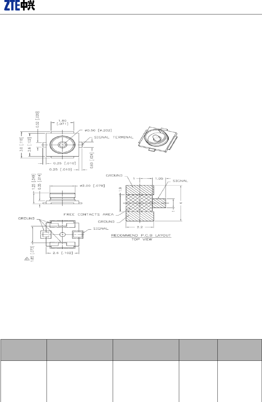
Program1:
PIN2isusedastheantennaPIN.Payattentiontothefollowing when using it as the antenna’s
feedPIN:
(1)ThefeedconnectedtoPIN2is50ohmmicro‐striporstripline.Toapproachthemodule,put
πshapeorFshapematchingnetworkforlatertuning.
(2)TheRFwiresmustbekeptawayfromtheGND,andgenerallythedistanceshouldbe3times
ofthewidthofRFwires.
(3)It’sforbiddentoputsomeinterferencesourcessuchasDCDC,WIFImodulearoundRFwires
Intend to OEM Integrator Installation
It’s not allowed to spread without the
permission of ZTE Corporation. © ZTE Corporation. All rights reserved. 第9页
orRFport
Program2:
WhenusingRFplugastheantennafeed,disconnectPIN2fromthemainboardandmakesure
therearesomecleanareasbeloworaroundPIN2.Keep2mmdistancebetweenthesurfaceofPIN2
andGND,anddrillholesbelowPIN2.It’snotsuggestedtousethecompatibledesignofPIN2atthe
sametimewhenusingtheRFconnector.
Figure2‐1Antennainterfacediagram
the maximum antenna gain is 3dBi for GSM850/WCDMA850 band and 5dBi for GSM1900/WCDMA1900
band.
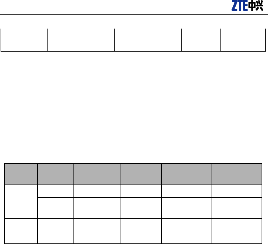
2.3 AntennaInterface’sRFPerformance
Seetheantennainterface’sRFperformanceintable2‐2:
Table2‐2AntennaInterface’sRFPerformance
MW3736_V1A:
Antenna
Interface’sRF
Performance
Module’suplink
(MS‐>BTS)
Module’sdownlink
(BTS‐>MS)
Power
(dBm)
Antenna
interfaceRx.
sensitivity
WCDMA850 824MHz‐849MHz 869MHz‐894MHz 23(+1/‐2) <‐110dBm
WCDMA1900 1850MHz‐1910MHz 1930MHz‐1990MHz 23(+1/‐2) <‐110dBm
GSM850 824MHz‐849MHz 869MHz‐894MHz 32+‐0.5 <‐108dBm
GSM1900 1850MHz‐1910MHz 1930MHz‐1990MHz 29+‐0.5 <‐108dBm
GPRS850 824MHz‐849MHz 869MHz‐894MHz 30+‐0.5 <‐108dBm
Intend to OEM Integrator Installation
第10 页 © ZTE Corporation. All rights
reserved. It’s not allowed to spread without the
permission of ZTE Corporation
GPRS1900 1850MHz‐1910MHz 1930MHz‐1990MHz 28.5±0.5 <‐108dBm
EDGE850
EDGE1900
824MHz‐849MHz
1850MHz‐1910MHz
869MHz‐894MHz
1930MHz‐1990MHz
32+‐0.5
30+‐0.5
<‐108dBm
<‐108dBm
3 Module’sElectricalCharacteristics
This chapter mainly introduces the module’s electrical characteristics, including module’s
interfacelevel,powerconsumption,reliability,etc.
3.1 Descriptionsofinterfacelevel
Table3‐1 Descriptionoflevelofmodule’smainexternalinterfaces
External
interfaces
High/low
level Min. Typical Max. Remarks
UART 0 0 0.3*V_UART
1 0.7*V_UART V_UART Internal voltage
conversion
UIM 0 0 0.3*VREG_RUIM
1 0.7*VREG_RUIM VREG_RUIM
Amongthem,V_UARTis1.8V,andVREG_RUIMis1.8V/2.85V.
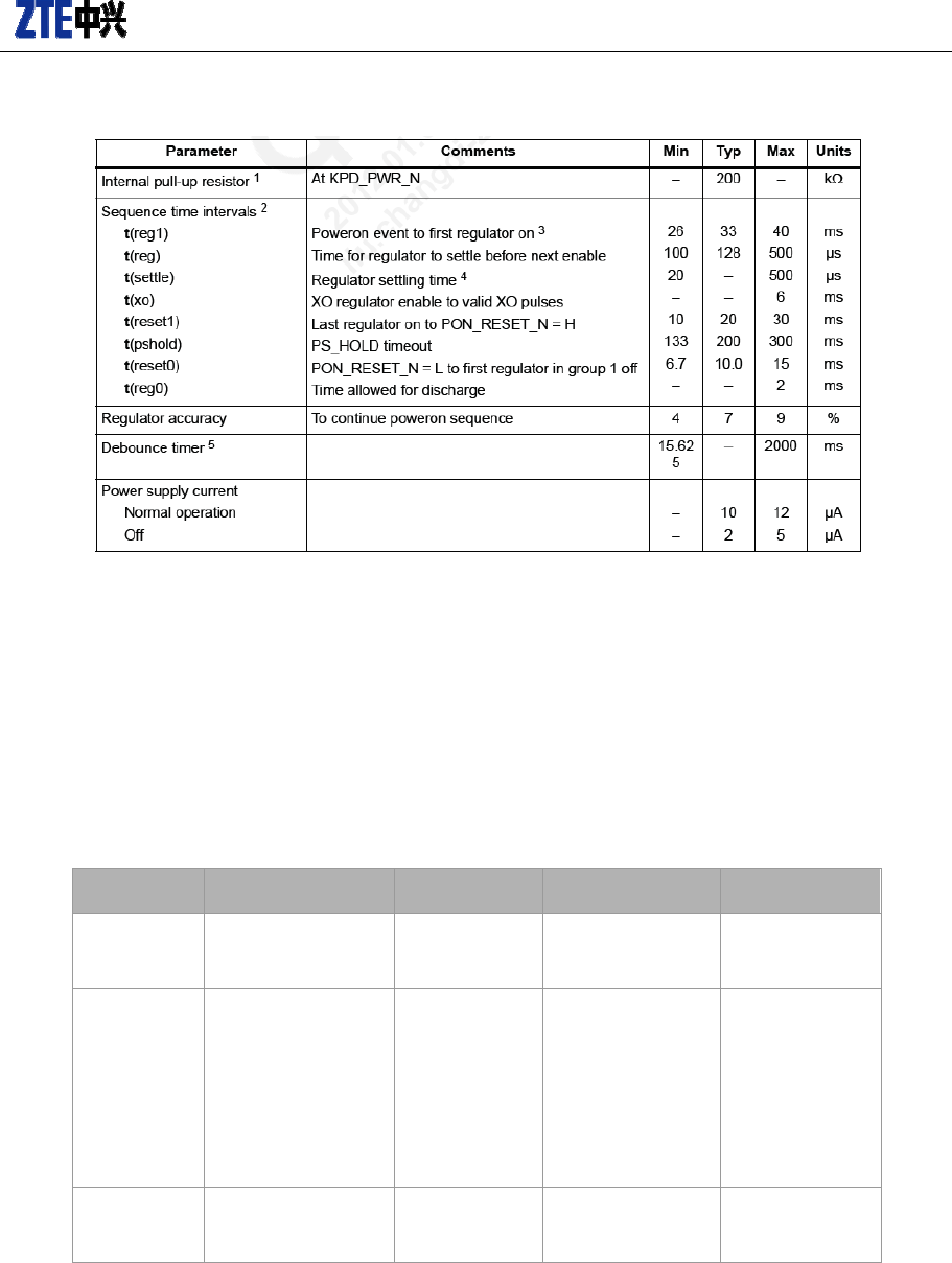
3.2 Poweron/offTimeSequence
Thetimesequencediagramindicatesthewholepoweron/offprocess.
Intend to OEM Integrator Installation
It’s not allowed to spread without the
permission of ZTE Corporation. © ZTE Corporation. All rights reserved. 第11 页
Table3‐1Poweron/offcircuittimecharacteristics
3.3 Reliability
Beforeleavingthefactory,themodulehasgonethroughaseries of reliability tests, such as:
high/low temperature operation, high/low temperature storage, thermal shock, alternating
temperature humidity, etc. The test results conform to the requirements in the industry. List the
module’sworktemperatureinthetablebelow:
Table3‐3Module’stemperaturecharacteristics
Parameters Descriptions Min. Max. Remarks
To Normal work
temperature
‐25℃+65℃
Ta Limited work
temperature ‐30℃ +75℃
Basic
functions are
normal, but
the RF
performance
slightlydrops.
Ts Module’s storage
temperature
‐40℃+85℃
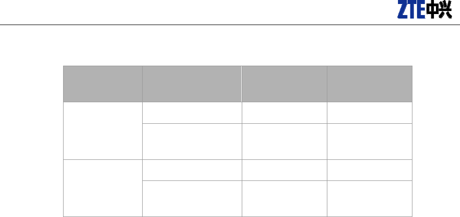
3.4 ESD
The module’s interface, antenna interface and UIM card interfaceallpassthestandardESD
performancetesting.
Intend to OEM Integrator Installation
第12 页 © ZTE Corporation. All rights
reserved. It’s not allowed to spread without the
permission of ZTE Corporation
Table3‐4Module’sESDcharacteristics
Interface Testitems Test
requirements Performance
Antenna
interface
Airdischarging ±8kV Nothingwrong
Contact
discharging ±6kV Nothingwrong
UIM card
interface
Airdischarging ±8kV Nothingwrong
Contact
discharging ±6kV Nothingwrong
Intend to OEM Integrator Installation
It’s not allowed to spread without the
permission of ZTE Corporation. © ZTE Corporation. All rights reserved. 第13 页
4 ReferenceDesignofInterfaceCircuits
Thischapterdescribesthereferencedesignofinterfacecircuitsandprecautionsaccordingtothe
module’sfunctions.
4.1 PowerandReset
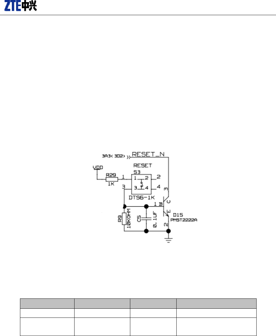
Seethereferencedesignofpowercircuitinfigure4‐1.
Figure4‐1Powerandresetcircuitreferencedesigndiagram
Powerdesign
ThemoduleispoweredbyVBAT.Seethevoltagecharacteristicsintable4‐1.
Table4‐1Voltagecharacteristics
Classification MIN TYPICAL MAX(instantaneous)
Inputvoltage 3.6V 3.7V 4.2V
Inputcurrent <3mA(average) ‐‐ 530mA(WCDMA)
1800mA(GSM)
Poweron
Themodulewillbenormallypoweredoffafterconnectedtothepowernormally.
Provideone4S~6Slowpulsetothemodule’sON/OFFpintoturnonthemodule.
The time required to power on at eachtimedependsonthemodule’s status. Usually, the low
levelmustlastforatleast4seconds.
Poweroff
Provideone4S~6Slowpulsetothemodule’sON/OFFpintoturnoffthemodule.

Intend to OEM Integrator Installation
第14 页 © ZTE Corporation. All rights
reserved. It’s not allowed to spread without the
permission of ZTE Corporation
Reset
Provideone3Slowpulsetothemodule’s/RESETpintoresetthemodule.
Afterreset,themodulewillenterthepower‐offstatus.Provideoneatleast4S lowpulsetothe
module’sON/OFFpintoturnonthemoduleagain.
V_MSME_1V8
ThereisavoltageoutputpinwithcurrentadjusteronMW3736module,whichcanbeusedtosupply
externalpowertotheboard.Thevoltageofthispinandthevoltageofbasebandprocessor/memory
comefromthesamevoltageadjuster.Thevoltageoutputisavailableonlywhenthemoduleison.The
normal output voltage is 1.8V, and the user should absorb the current from this pin as little as
possible(lessthan10mA).Generally,itisrecommendedtousethispinforpull‐upwhenmatchingthe
level.
OtherAdvice
Inordertomakesurethedataissavedsafely,pleasedon’tcutoffthepowerwhenthemoduleis
on. It’s strongly recommended to use the soft switch to turn off the mobile phone. If the interval
betweenthecut‐offandpower‐onislessthan2seconds,itwouldcausethemoduletoautomatically
poweron.
4.2 COMPort
The module provides a full duplex UART interface, whose maximal data rate is 230.4kbps and
typicaldatarateis115.2kbps.TheexternalI/Olevelis1.8VCMOSsignal.
Precautions:
1)Themodule’sI/Olevelis1.8VCMOS,andthelevel conversion is required whenconnected
withstandard3.3Vlogiccircuit.(e.g.,MCUorRS232driverchipMAX3238).Otherwise,itmightcause
unstablecomportsbecausethelevelisnotmatchedorcausedamagetothemodulebecauseitisat
highlevelforalongtime.
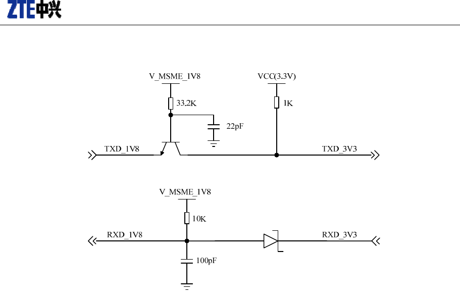
Fornon1.8VexternalUART,itneedstoconvertthelevel.Normallyadynatronisusedtorealize
the level conversion. As shown in figure 4‐2, the resistance is just for your information, please
calculateagainduringthedesign.ThediodeinthefigureisSchottky diode (forward voltage drop:
0.3V).Ifyouselectotherdiode,pleaseselectonewithsmallerforwardvoltagedroptoguaranteethat
RXD_1V8’slevelisbelowthethresholdwheninputtinglowlevel.
2)Portbaudrate115200(bydefault),canbeusedforATcommandsandMODEM.Thehardflow
controlisOFFbydefault.
Intend to OEM Integrator Installation
It’s not allowed to spread without the
permission of ZTE Corporation. © ZTE Corporation. All rights reserved. 第15 页
Figure4‐2 UARTinterfacelevelconversion
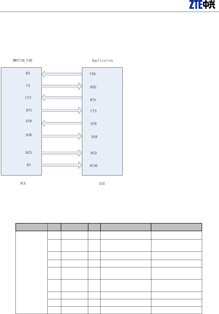
4)ConnecttoRXDandTXDonlywhenthereisnoflowcontrolinuse;
Whenusinghardwareflowcontroltoconnectotherprocessors,useRXD,TXD,/CTSand/RTS;
whenusedasModemtoconnecttothePC,connectallIOsignalcables(8wires).Besides,theringtone
signalwillproducelowlevelinterruptionupon anincomingcallortextmessage.SelecttheportIO
signalsforlevelconversionaccordingtothespecificconditions.
Intend to OEM Integrator Installation
第16 页 © ZTE Corporation. All rights
reserved. It’s not allowed to spread without the
permission of ZTE Corporation
DescriptionsofUARTinterface:
Figure4‐3UARTDCE-DTEconnectionrelationshipdiagram
SeethedefinitionsofUART1interfaceintable4‐2.
Table4‐2DefinitionsofUART1interface
Classification No. Definitions I/O Descriptions Remarks
UART
(1.8V)
22 UART_RX I Receivedata DTEtransmitsserialdata
25 UART_RTS O Readytosend DTEinformsDCEto
send
23 UART_TX O TransmitdataDTEreceivesserialdata
26 UART_DTR I Dataterminalready DTEisready
21 UART_CTS I Cleartosend DCEhasswitchedtoRx.
mode
24 UART_RI O Ringtoneindication InformDTEupona
remotecall
28 UART_DSR O Datasetready DCEisready
27 UART_DCD O Carrierwavedetection Datalinkconnected
GND GND
Intend to OEM Integrator Installation
It’s not allowed to spread without the
permission of ZTE Corporation. © ZTE Corporation. All rights reserved. 第17 页
4.3 UIMcardInterface
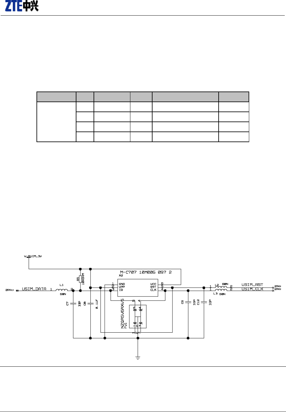
Themodulesupports1.8V/2.85VUIMcard.Seethedesigninfigure4‐3.It’srecommendedtoadd
ESDtoprotecttheUIMcard.
Table4‐3UIMcardinterfacedefinitions
Classification No. Definitions I/O Descriptions Remarks
UIM 1 V_RUIM O RUIMcardvoltage
2 UIM_RST O RUIMcardrest
3 UIM_CLK O RUIMcardclock
4 UIM_DATA I/O RUIMcarddata
ThetypicalratevalueofUIMcardinterfaceisabout3.25MHz,thereforetheUIMcardsocketshould
beputnearthemodule’sinterfacetoavoidseriouswaveformdeformationcausedbyoverlongwiring
(it’sadvisedthatthewiringshouldnotexceed100mm),otherwise,itwillaffectthesignal
communication.
ThewiringofUIM_CLKandUSIM_DATAshouldbeenvelopedbythegroundwires.Addone0.1uFor
0.22uFcapacitancetoV_RUIM,andadd33pFcapacitancetoUIM_CLK,UIM_DATA&UIM_RSTtofilter
theinterferenceofantennasignals.Besides,theanti‐staticperformanceofthesefoursignalscanbe
realizedthroughtheTVStubeorESDcomponent.Seethefigurebelowforthereferencedesign.
Figure4‐4UIMcardcircuitreferencedesign
Note:
The PCB wiring of UIM card should be laid closely around the module as possible as you can, and the
ESD component should be put near the UIM card socket.
Intend to OEM Integrator Installation
第18 页 © ZTE Corporation. All rights
reserved. It’s not allowed to spread without the
permission of ZTE Corporation
4.4 AudioInterface(optional)
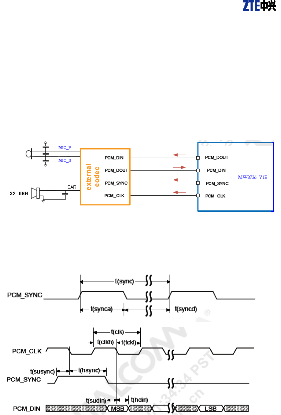
ThemoduleprovidesonePCMinterface,whichmustconnectoneCODECexternallytoinputand
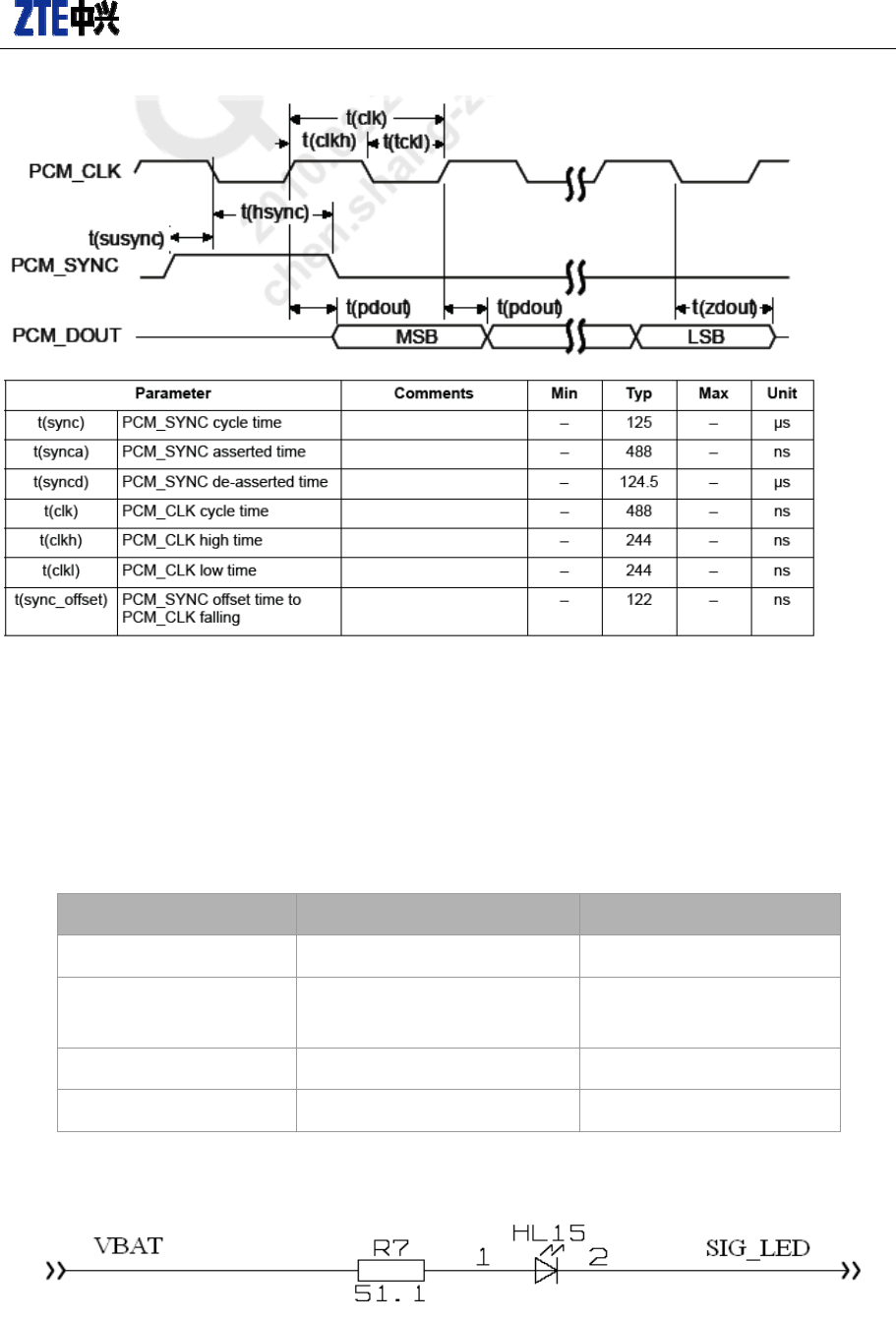
outputaudios.Themodule’sPCMinterfaceprovidesPCM_CLK,PCM_SYNC,PCM_DIN,PCM_DOUT,and
itsupports2.048MHzPCMclockdatarateand8Kframedatarate.PCMclockwillstoptheoutput
whenitentersthedormantmode.
Themodule’sPCMinterfacemustworkunderMastermode,andtheclockandSYNCsignalmust
besentbythemodule.ThedeviceconnectedwiththeinterfacecanworkunderSlavemodeonly.
Seetheaudiointerfacecircuitinfigure4‐4.
Figure4‐5Audiointerfacecircuitreferencedesignprinciplediagram
Codecaudiointerfacedesignontheheadset
ThetwomicrophoneinterfacesMIC_NandMIC_Parebothdifferential interfaces, which could
also be used for single‐end input. It’s recommended to use differential mode to reduce the noises.
RefertotheconnectionofEARleft/rightchannelinthefigure.
SeethetimesequenceofPCMinterfaceinfigure4‐5.
Intend to OEM Integrator Installation
It’s not allowed to spread without the
permission of ZTE Corporation. © ZTE Corporation. All rights reserved. 第19 页
4.5 WorkStatusIndicators
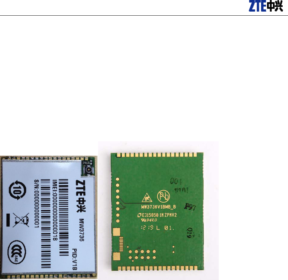
TheSIG_LEDPINoutputstatusisdefinedbythesoftware.TheSIG_LEDPINisMPPport,which
candrive20mAcurrent.Seethereferencedesignofindicatorsinfigure4‐5.
Table4‐4Descriptionofworkstatusindicators
Modulestatus Indicatorstatus Frequency
Power‐onstatus Slowflash 1Hz
Network searching
status Standardflash 3Hz
IDLEstatus Slowflash 1Hz
Trafficstatus Fastflash 5Hz
Figure4‐5Indicatorreferencedesignprinciplediagram
Intend to OEM Integrator Installation
第20 页 © ZTE Corporation. All rights
reserved. It’s not allowed to spread without the
permission of ZTE Corporation
5 MechanicalDesign
5.1 AppearanceDiagram
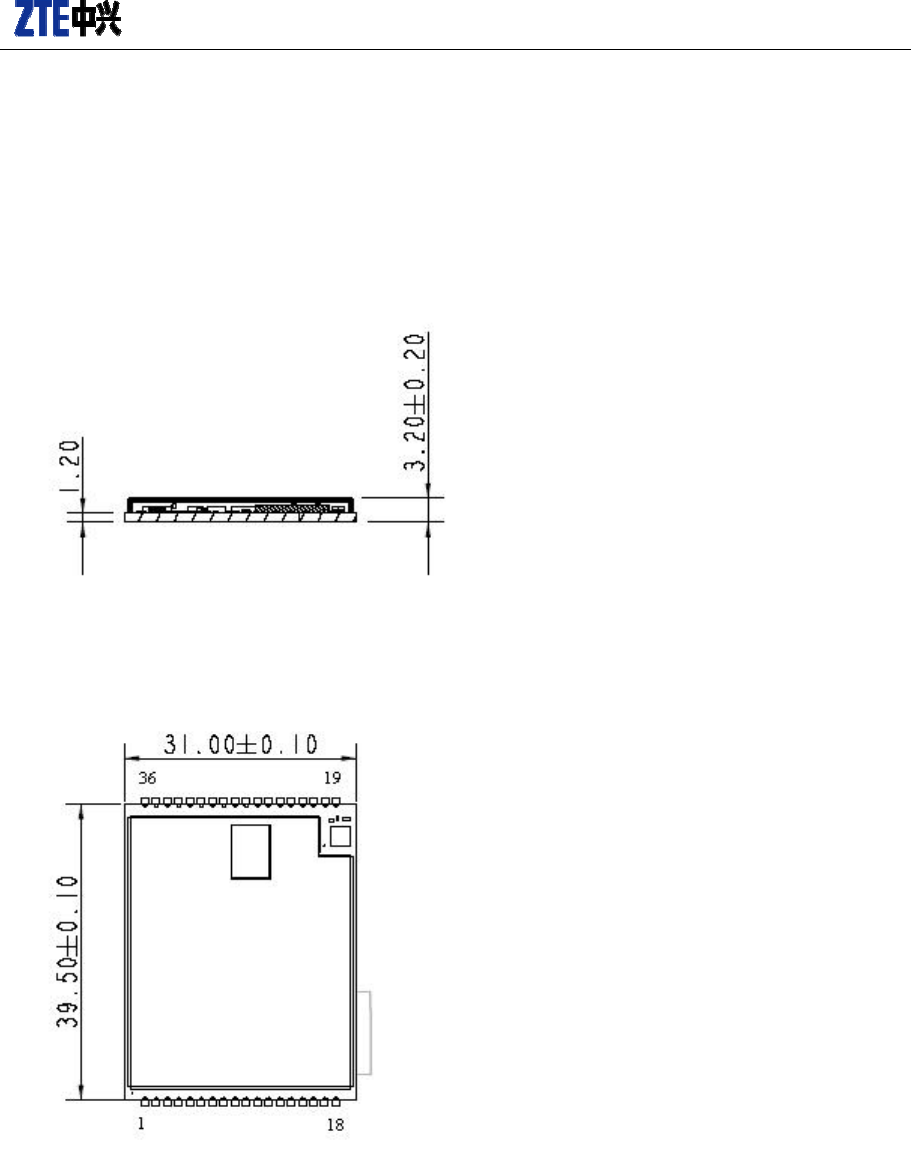
SeeMW3736module’sappearanceinfigure5‐1.
Figure5‐1MW3736module’sappearancediagram
Dimensions:39.50mm×31.00mm×2.65mm
Weight:10g
Intend to OEM Integrator Installation
It’s not allowed to spread without the
permission of ZTE Corporation. © ZTE Corporation. All rights reserved. 第21 页
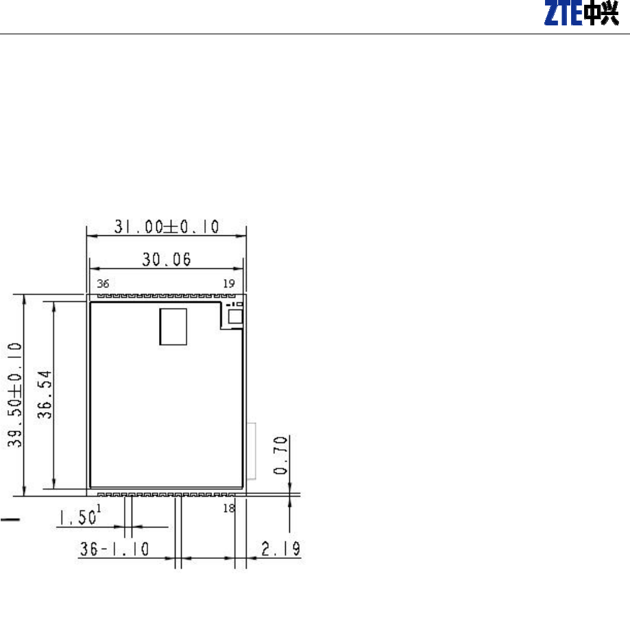
5.2 Module’sAssemblyDiagram
Seetheassemblydiagramofthemoduleinfigure5‐2.
Figure5‐1Module’sassemblydiagram
Intend to OEM Integrator Installation
第22 页 © ZTE Corporation. All rights
reserved. It’s not allowed to spread without the
permission of ZTE Corporation
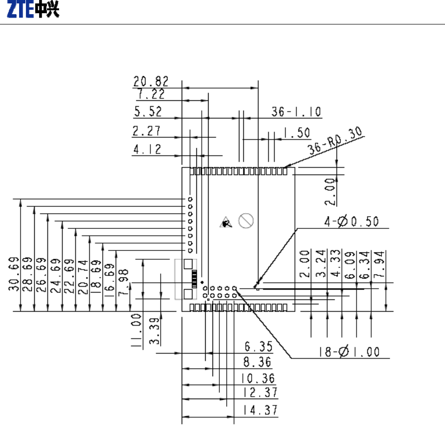
5.3 Module’sPCBEncapsulationDimensions
Seethemodule’sPCBencapsulationdimensionsinfigure5‐3.
Figure5‐2PCBencapsulationdiagramofrelevantfemalesocket(topview)
Intend to OEM Integrator Installation
It’s not allowed to spread without the
permission of ZTE Corporation. © ZTE Corporation. All rights reserved. 第23 页
Figure5‐4PCBencapsulationdiagramofrelevantfemalesocket(bottomview)
PrecautionswhiledesigningPCB:
1) Copper‐cladandwiringareforbiddenoneachlayerofthePCBattheareabelowtheRFtest
points.
2) Fortheconvenienceoftestingandmaintenance,itmightbenecessarytodrillholesonthe
PCBtoexposeJ‐TAGtestpoints.