ZTE ZTEWelink MF206A Module Specification V1.2
User Manual: ZTE ZTE MF206A - ZTE USA
Open the PDF directly: View PDF ![]() .
.
Page Count: 4

Version:1.2
Date:2013-05-31
Product Spec List
Product Name:MF206A

Version Date Revised by Reviewer Reason for Revision
V1.1 The initial version
V1.1.1 2013-2-27 increase the version history
2013-4-1
Change the logo of cover and
header,footer;Add the voltage of sleep
mode.Modify the approval of GCF to
optional;Add the support of Android
4.0; Add the notes of MMS.
2013-5-31 Release as Version 1.2
Version History
V1.2
ZTEWelink MF206A Module Specification
Item Feature
Complia
nce
Notes
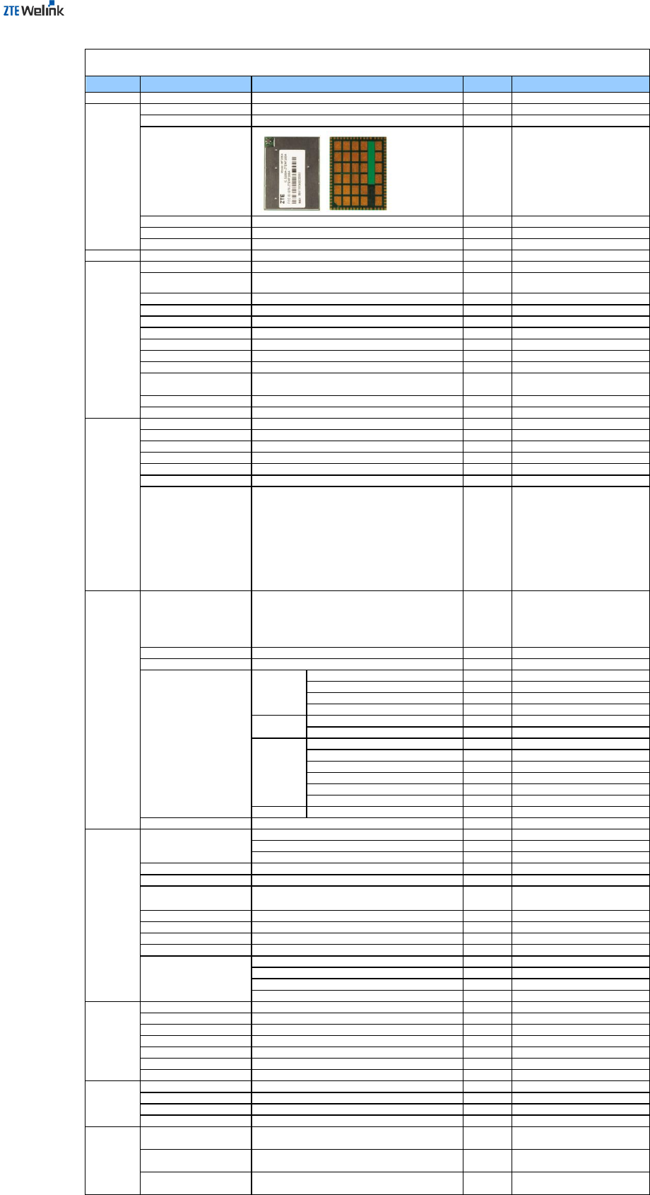
Product Name
Dimensions
Weight
Picture
Form Factor
USB Interface Type Provide USB Interface
Design guide Yes
Solution Chipset supplier
Processor
Processor speed (Apps)
USIM/SIM 3V SIM card and 1.8V SIM card
Memory(SDRAM/NAND) Cost Related
MICRO SD Card Optional
USB Version
Interface
Active power consumption W2100, Average Power 0dBm
Sleep Mode
Minimum power
consumption
-75db ,DRX =640
Power supply
LED control
Receive Diversity No
Main Antenna Provide Antenna Interface or pad
Receive Diversity Antenna
GSM Band Cost Related
UMTS Band Cost Related
RxDiv Band
Max. transmitter power
GSM/EDGE/WCDMA
HSDPA/HSUPA/HSPA+
3GPP Release
Windows XP (SP2 and later) Yes
Windows Vista (32bit) Yes
Windows Vista (64bit) Yes
Windows 7 Yes
WinCE 5.0 Yes CPU:X86、ARM
WinCE 6.0 Yes CPU:X86、ARM
1.6 Yes
2.0 Yes
2.1 Yes
2.2 Yes
2.3 Yes
4.0 Yes
Linux kernel 2.6.20 and later Yes
GPRS Class
Yes
Optional Windows
Optional Linux
GPS Yes
SMS Yes
MMS Yes
not support build-in MMS protocol
stack
STK Yes
USSD Yes
PHONEBOOK Yes
NETWORK LOCK Optional
Yes
Yes
Yes
Yes
CE Yes
GCF Optional
FCC Yes
ROHS Yes
PTCRB Yes
CCC Optional
Others Yes
Operating Temperature
Limited Temperature
Storage Temperature
Humidity
Engineering samples Date
(yyyy/mm/dd)
Final samples Date
(yyyy/mm/dd)
Product Market launch Date
(yyyy/mm/dd)
MF206A Spec List
Artwork
Baseband
RF
Hardware & Software Design guide
Qualcomm
ARM 9
MDM6270:High-performance ARM926EJ-S running at
up to 184 MHz for 3.6 Mbps HSDPA
Support Standard 6 PIN SIM card
about 170mA
Approvals
&Certification
Envionment
Commercial
Details
OS
Class B
≤75mA
N/A
-30 ~ 75° C
GSM CS: UL 9.6kbps/DL 9.6kbps
GPRS: Multi-slot Class 10
EDGE: Multi-slot Class 12
WCDMA CS: UL 64kbps/DL 64kbps
WCDMA PS: UL 384kbps/DL 384kbps
LGA package type II(108 Pin)
Other
WinCE
Technical
Standard
External
N/A
USB 2.0 HIGH SPEED
LGA
Android
EDGE/GPRS/GSM:1900/1800/900/850MHz
R99,R5
Window
About 5.2g
HSDPA: DL 3.6Mb/s(Category 6)
3.8V(3.4~4.2V)
WCDMA/HSDPA:2100/1900/850(900)MHz
3 LED pins
32MByte/128MByte
about 3.9mA
UMTS2100/1900/850(900): Power Class 3 (+24dBm
+1/-3dBm)
GSM/GPRS 850MHz/900MHz: Power Class 4
(+33dBm ±2dBm)
GSM/GPRS 1800MHz/1900MHz: Power Class 1
(+30dBm ±2dBm)
EDGE 850MHz/900MHz: Power Class E2 (+27dBm ±
3dBm)
EDGE 1800MHz/1900MHz: Power Class E2 (+26dBm
-4/+3dBm)
2011-5-20
Description
-40 ~ 85° C
-45 ~ 90° C
5%~ 95%
2011-1-20
MF206A
36mm * 26mm * (2.5+/-0.2)mm
IC、WEEE
2011-3-20
POWER SUPPLY
RF Switch
Standby & Hibernation
USB Selective Suspend
Remote Wake-up
Application
DATA
RAS
NDIS
ECM
© 2013 ZTEWelink Corporation. All rights reserved. 3/4
ZTEWelink MF206A Module Specification
Pin Pin Name Description I/O Remark
1 ANT_MAIN Main antenna pad AIO
2 GND Ground
3 JTAG_RESOUT_N JTAG reset signal DI Reserved for ZTEWelink debug
4 PON_RST_N Module reset DI 1.8V
5 POWER_ON Power on/off DI 1.8V
6 AP_READY Module query AP sleep status DI 1.8V; L: Active H: Sleep
7 I2C_SCL I2C clock DO
8 I2C_SDA I2C data DIO
9 MODULE_READY AP query module sleep status DO 1.8V; L: Active H: Sleep
10 AP_WAKEUP_MODULE AP wake up module DI 1.8V; L: valid H: invalid
11 MODULE _WAKEUP_AP Module wake up AP DO 1.8V; L: valid H: invalid
12 GND Ground
13 RESERVED
14 GND Ground
15 NC
16 NC
17 NC
18 NC
19 MODULE_POWERON Module status indicator DO 1.8V; L: Shut down H: Power on
20 LED_GREEN AI
21 LED_RED AI
22 LED_BLUE AI
23 VPH_PWR
24 VPH_PWR
25 VPH_PWR
26 VPH_PWR
27 UART_CTS UART Clear To Send signal DI
28 UART_RFR UART Request To Send signal DO
29 UART_TXD UART Transmit Data output DO
30 UART_RXD UART Receive Data input DI
31 GND Ground
32 RESERVED
33 RESERVED
34 RESERVED
35 RESERVED
36 GND Ground
37 ADC Anolog voltage detect AI 0~2.1V
38 GND Ground
39 SPI_CS_N
SPI chip-select; not mandatory in a
point-to-point connection
DIO
40 SPI_CLK SPI clock DIO
41 SPI_DATA_MI_SO SPI master out/slave in data DIO
42 SPI_DATA_MO_SI SPI master in/slave out data DIO
43 USB_VBUS Monitors the external USB supply voltage AI
44 GND Ground
45 USB_DP The postive USB differential signal AIO
46 USB_DM The negtive USB differential signal AIO
47 GND Ground
48 VREG_RUIM Power for SIM AO
49 UIM_DATA Data for SIM DIO
50 UIM_CLK Clock for SIM DO
51 UIM_RST Reset for SIM DO
52 UIM_DP Be used for UICC AIO
53 UIM_DM Be used for UICC AIO
54 GND Ground
55 VREG_SDCC SD CARD power supply AO
56 SDCC_CMD Command bit for SD device DIO
57 SDCC_CLK Output clock for SD device DO
58 SDCC_DATA3 SD device data bit3 DIO
59 SDCC_DATA2 SD device data bit2 DIO
60 SDCC_DATA1 SD device data bit1 DIO
61 SDCC_DATA0 SD device data bit0 DIO
62 SD_DET_N SD device detect DI 1.8V
63 GND Ground
64 RESERVED
65 RESERVED
66 GND Ground
67 RESERVED
68 RESERVED
69 GND Ground
70 GPS_ANT GPS antenna AI
71 GND Ground
72 JTAG_TRST_N JTAG reset
73 JTAG_RTCK JTAG return clock
74 JTAG_TCK JTAG clock input
75 JTAG_TDO JTAG test data output
76 JTAG_TDI JTAG test data input
77 JTAG_TMS Test mode select input
78 GND Ground
79~108 GND_PAD Thermal Pads Ground
Notes:
1. DI:Digital input, DO:Digital output,DIO:Digital output & Digital output
2. AI:Analog input, AO:Analog output,AIO:Analog output & Analog output
1.8V
Reserved for ZTEWelink debug
MF206A PIN Define
Valid Current:
5/10/15/20/25/30/35/40mA
3.8V(3.4~4.2V)
1.8V
USB slave
High-speed
SIM card type: 1.8/3.0V
Supprot UICC
1.8V
LED Indicator pins
Power supply
AI
© 2013 ZTEWelink Corporation. All rights reserved. 4/4
