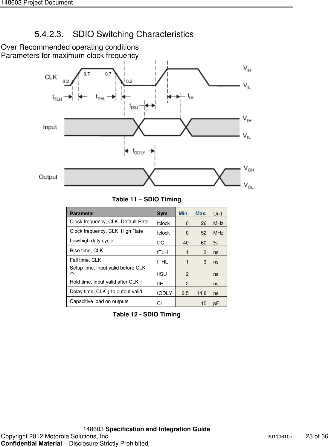
Zebra Technologies 211486030A 21-148603-0A User Manual
Zebra Technologies Corporation 21-148603-0A
UserManual.wiki
>
Zebra Technologies
>
211486030A User Manual
User Manual
Navigation menu
Upload a User Manual
Namespaces
Wiki Guide
HTML
PDF
Info
Views
User Manual
Discussion / Help
Navigation
![148603 Project Document Copyright 2012 Motorola Solutions, Inc. 20110610-i i Confidential Material – Disclosure Strictly Prohibited. "Ni ckel Leucochroic Puffin" Motorola Solutions Inc. Title: 148603 Specification and Integration Guide Description/Abstract/Synopsis: The purpose of this document is to provide an integration guide targeted for module integrators who have an NDA with Motorola Solutions. Document Status: In Progress A [ ] – Released Version MPA Document Number: [ ] – Next Release In Process NA Division: Sub-team: [ ] – Document Obsolete Working Revision: 20110610-i MCD RF-SYS Obsolete Document Replaced By: Last Updated: 01/18/2012 Document Type: SPEC / IG N/A Confidentiality Statement: Classification: N/A [] - Contains Motorola Solutions partner NDA related material (Disclosure requires a three-way NDA.) Partner Name Agreement Number USI Under NDA and Motorola Corporate Supply Agreement between Motorola Solutions and USI [] - For Motorola Solutions Internal Use Only [ x] - Disclosure allowed under Motorola Solutions NDA Only [x] - Does or may contain Motorola Solutions patentable property *** Direct this document‟s disclosure inquires to (Job Title): TNT Archive Location/Path: Agile Current Owner: Authors / Contributors: Revision History](https://usermanual.wiki/Zebra-Technologies/211486030A/User-Guide-1674497-Page-1.png)
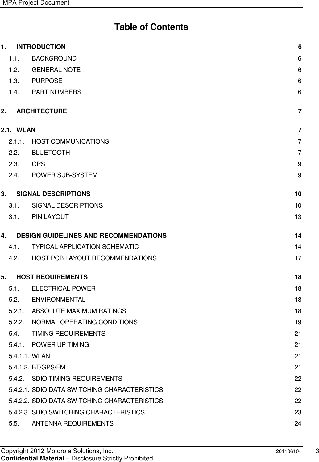
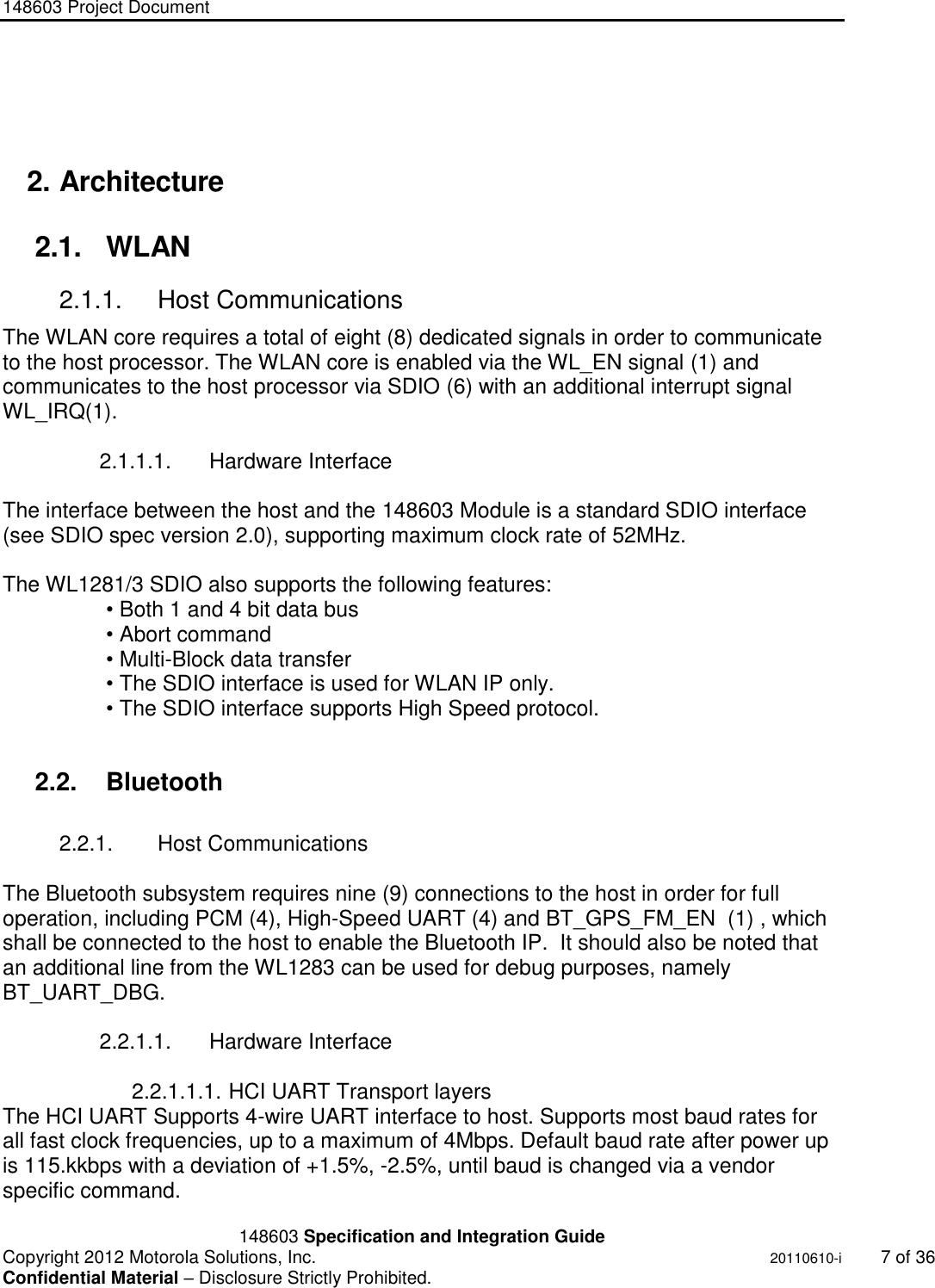
![148603 Project Document 148603 Specification and Integration Guide Copyright 2012 Motorola Solutions, Inc. 20110610-i 10 of 36 Confidential Material – Disclosure Strictly Prohibited. "Ni ckel Leucochroic Puffin" 3. Signal Descriptions 3.1. Signal Descriptions Listed below are the pin numbers and signals on the 148603 module. GEN = General (No specific function), PWR= Power Supply, ANA= Analog NOTE: FM is DISABLED in all revisions, and WLAN RF0 Path is not populated in the -01 and -02 versions. Table 2 – Signal Descriptions PIN DEFINE REV 0.02 Module Pin Name Pin # I/O Type Function Connects to SD State Default State (after POR) Buffer [mA] Description VBAT1 68 PWR GEN PWR VBAT 3.3V Input VBAT2 69 PWR GEN PWR VBAT 3.3V Input VBAT3 70 PWR GEN PWR VBAT 3.3V Input VBAT4 71 PWR GEN PWR VBAT 3.3V Input VIO1 16 PWR GEN PWR VIO 1.8V Digital Voltage VIO2 17 PWR GEN PWR VIO 1.8V Digital Voltage GND1 6 GND GEN GND Ground Pin GND3 8 GND GEN GND Ground Pin GND4 10 GND GEN GND Ground Pin GND5 11 GND GEN GND Ground Pin GND6 13 GND GEN GND Ground Pin GND7 14 GND GEN GND Ground Pin GND8 15 GND GEN GND Ground Pin GND9 18 GND GEN GND Ground Pin GND10 23 GND GEN GND Ground Pin GND11 30 GND GEN GND Ground Pin GND12 33 GND GEN GND Ground Pin GND13 36 GND GEN GND Ground Pin GND14 38 GND GEN GND Ground Pin GND15 41 GND GEN GND Ground Pin GND16 43 GND GEN GND Ground Pin GND17 46 GND GEN GND Ground Pin GND18 48 GND GEN GND Ground Pin GND19 50 GND GEN GND Ground Pin GND20 54 GND GEN GND Ground Pin GND21 60 GND GEN GND Ground Pin GND22 67 GND GEN GND Ground Pin](https://usermanual.wiki/Zebra-Technologies/211486030A/User-Guide-1674497-Page-10.png)