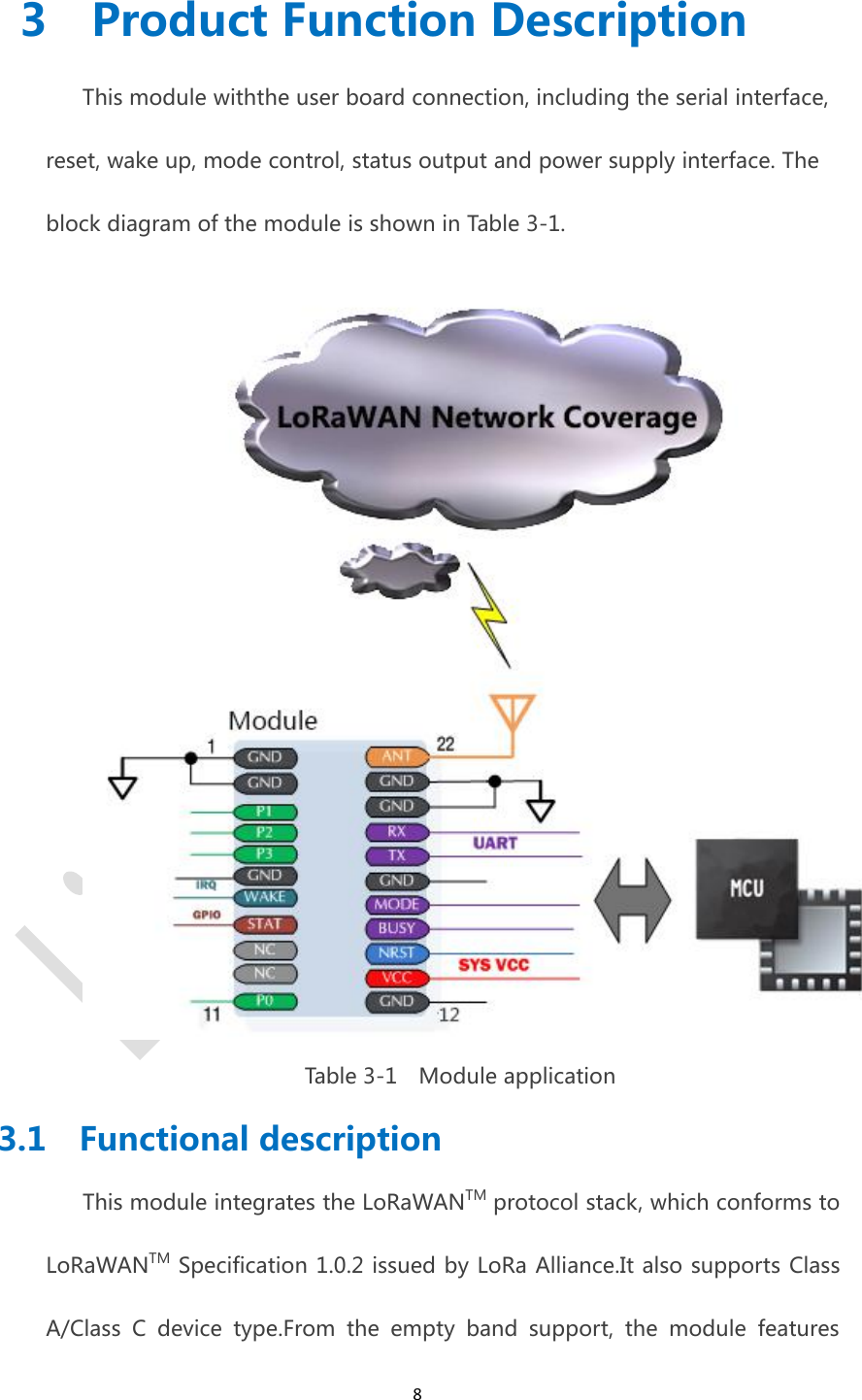
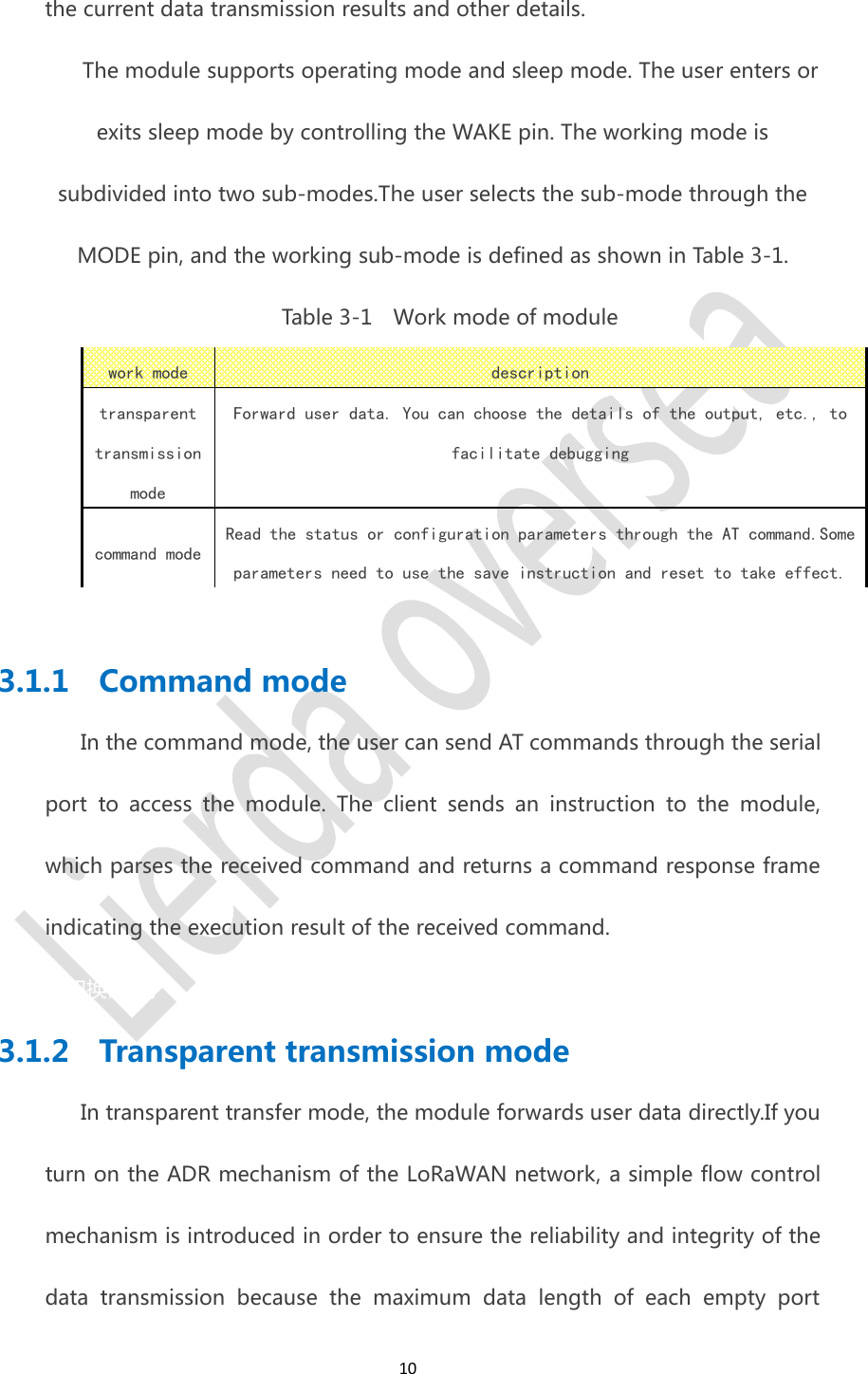
Zhejiang Lierda Internet of Things technology LSD4WN2L917M90 LoRaWAN System Node (US915) User Manual

Zhejiang Lierda Internet of Things technology Co.,Ltd LoRaWAN System Node (US915)

User Manual

1LSD4WN-2L917M90 User Manual  Documentation Edition:Rev02 Recently updated:March 15, 2017
2Document revision historyversion revision date revision note1.0.0 2017-10-30 Initial version
3Catalogue1 Summary............................................................................................................................42 Product technical parameters......................................................................................53 Product Function Description...................................................................................... 83.1 Functional description............................................................................................... 83.1.1 Command mode............................................................................................ 103.1.2 Transparent transmission mode.................................................................... 104 Mechanical properties................................................................................................. 134.1 Product appearance.................................................................................................134.1 Module assembly drawing.......................................................................................134.2 Module Board PCB Package Dimensions.................................................................145 Interface specification................................................................................................145.1 Pin definition............................................................................................................145.2 Hardware interface description............................................................................... 165.2.1 External power.............................................................................................. 165.2.2 Reset..............................................................................................................175.2.3 Mode control................................................................................................. 175.2.4 UART interface............................................................................................. 185.2.5 Module status indication...............................................................................195.2.6 Sleep control................................................................................................. 215.2.6 Extended GPIO............................................................................................. 215.3 Typical application circuit.........................................................................................225.3.1 Antenna design proposal...............................................................................23
41 SummaryLSD4WN-2L917M90 is a LoRaWAN End Node module developed by Lierda Technology Group.This module integrates the LoRaWANTM protocol stack, which conforms to LoRaWANTM Specification 1.0.2 standard issued by LoRa Alliance.Hardware support 902.3-926.8 MHz ultra-wide band.The module uses the serial interface to communicate with the user equipment data, instruction interaction.It can easily provide users with fast LoRaWAN network access and wireless data services.LSD4WN-2L917M90 module with low power consumption, transmission distance, anti-interference ability, suitable for a variety of applications: Internet of things low power applications (IoT), automatic meter reading, smart city, industrial automation, smart home.Product featuresworking voltage:DC 2.5-3.6V ;physical layer:NA915;Transmit power:17.0±1.5dBm(max);Ultra-high reception sensitivity:-135±1dBm(@SF=12);Far away from the effective communication distance:5Km(Urban roadenvironment,Non-wilderness environment);Meet LoRaWANTM Specification 1.0.2 standard;Internal integration LoRaWANTM protocol stack, support Class A \ Class Cdevice type;
5Low power consumption: standby current ≤ 2.0 uA;UART communication, external interface for the stamp hole, simplecommand configuration module parameters.2 Product technical parametersThe technical parameters of this module are described below, including theprotocol standard, interface characteristic, mechanical characteristic, DCcharacteristic parameter, RF characteristic parameter and environmentalcharacteristic parameter.Table 2-1 Module technical parametersparametercontentprotocolstandarddescribeRemarksprotocol versionLoRaWANTM Specification1.0.2Update time June 2017physical layerNA915net topologyStarAccess LoRaWAN gateway,the formation of star -star network topologydevice typeClass A\Class CDo not support Class BNetwork access modeOTAA\ABPSend addressing modebroadcastmodulation modeLoRadata rateSF12~SF7Interfacecharacteri-sticsSerial interface2 wire UARTcompatible3.3V TTL\CMOSSerial baud rate2400\4800\9600\38400\19200\115200bpsThe user can configurethe serial baud rate ofthe transparent mode,and the command mode is
6fixed to 9600 bps.Main antennainterfaceStamp hole 50Ω outputMechanicalpropertiesInterface packagetypeStamp hole(2×11pin×2.0mm)PCBA size25.5(L) ×22(W) ×3.5(H)mm(GB/T1804-c)Table 2-2 DC characteristic parameterMainparametertest conditionleastvaluerepresentative valuecrestvalueunitremarksworkingvoltage-2.53.33.6VGuaranteedmaximumoutputpower20dBmworkingcurrentaveragecurrentnormalwork,9600Bps-2.4-mARTC on-23uApeak pointcurrent;maximum output--135mATable 2-3 RF characteristic parametersMainparametertest conditionleastvaluerepresentative valuecrestvalueunitremarksWorking bandest voltage:3.3VTest temperature:room temperature902.3 914.5 926.8MHzemissioncharacterist-icCarrier output,PA_BOOST ON,25℃ambient temperature
7MaximumtransmitpowerPA_BOOSToutput,Power fullload,use 9020Aspectrometer totest18.09 17.33 16.41dBmsecondharmonic-40dBmemissioncurrent(RF part)RF maximumtransmit poweroutput,instrument load120mAthe currentis related tothe antennaenvironmentReceivingcharacterist-icsPER = 1%,CR = 4/6,CRC ON,Preamble Length = 12,Packet Length = 10receivingsensitivitySF12--136-dBmflatness<0.5dBSF7--123-dBmreceivecurrent(RF part)-13-mAfrequencycharacterist-icfrequency stability:15ppm@-40℃~85℃Table 2-4 Environmental characteristic parametersmainparametertest conditionleastvaluerepresentative valuecrestvalueunitremarksworkingtemperature--40-+85℃Storagetemperature--40-+125℃workinghumidity-5-95%ESD protect---TBDV
83 Product Function DescriptionThis module withthe user board connection, including the serial interface,reset, wake up, mode control, status output and power supply interface. Theblock diagram of the module is shown in Table 3-1.Table 3-1 Module application3.1 Functional descriptionThis module integrates the LoRaWANTM protocol stack, which conforms toLoRaWANTM Specification 1.0.2 issued by LoRa Alliance.It also supports ClassA/Class C device type.From the empty band support, the module features
9include:a)LoRaWAN NA915 applicationThis module interacts with the user through the serial port.The module operating mode is designed for transparent mode andcommand mode.The user configures the LoRaWAN network parameter in the commandmode via the AT command (if not configured, the default parameterconfiguration will be used).Module in the transparent mode, the user canconfigure the parameters by using serial data transceiver, requiring themodule to output detailed information (the remaining data, RSSI, packet size,the number of retransmission, etc.).After receiving a frame of data, the BUSYpin is pulled low (busy) until the data transfer is completed (success orfailure).If the transmission fails, the STAT pin is pulled low while the BUSY pin ishigh (not busy).The STAT pin returns to the high state when the user writes anew frame of data or reads the transmission failure message through thecommand mode.For the first time, you need to configure the necessary network parametersof the module and execute the save command. Then, reset the module (themodule initializes the network with the new parameters) and switch to thetransparent mode.The module will automatically join the set LoRaWAN network. The user candetermine the status of the STAT pin and enter the command mode to query
10the current data transmission results and other details.The module supports operating mode and sleep mode. The user enters orexits sleep mode by controlling the WAKE pin. The working mode issubdivided into two sub-modes.The user selects the sub-mode through theMODE pin, and the working sub-mode is defined as shown in Table 3-1.Table 3-1 Work mode of modulework modedescriptiontransparenttransmissionmodeForward user data. You can choose the details of the output, etc., tofacilitate debuggingcommand modeRead the status or configuration parameters through the AT command.Someparameters need to use the save instruction and reset to take effect.3.1.1 Command modeIn the command mode, the user can send AT commands through the serialport to access the module. The client sends an instruction to the module,which parses the received command and returns a command response frameindicating the execution result of the received command.2 完成后,再处理这个模式切换请求。3.1.2 Transparent transmission modeIn transparent transfer mode, the module forwards user data directly.If youturn on the ADR mechanism of the LoRaWAN network, a simple flow controlmechanism is introduced in order to ensure the reliability and integrity of thedata transmission because the maximum data length of each empty port
11packet may change dynamically.1)、Flow control mechanismThe user determines the length of a frame of data. When the serial portexceeds the 2-byte transmission time does not receive the new serial data dataor reaches the FIFO storage limit, it is judged that one frame of datatransmission is completed.It immediately pull down the BUSY pin (busy) andthe serial port is received and the sending operation is performed. After thetransmission is complete (successful or failed), the BUSY pin is re-pulled high,and if the WAKE pin is still high, re-enable the module's serial port reception.2)、Physical subcontracting mechanismThe actual physical packetization is determined by Network Server, and theuser can query the response parameters via the AT command or requestdetailed information to obtain the packet case.In general, the maximum load value N corresponding to different rates isshown in Table 3-2.Table 3-2 The maximum load value corresponding to the different ratesSFN(MAX)722282229115105111511251
123)、Server responseAccording to LoRaWAN network Class A operating characteristics, for anypacket of data, the user server can give a response. If the module receives theuser server data, it will immediately output through the serial port. Therefore,due to the reason for the data frame packet, the user's one frame of data mayreceive a number of response packets.
134 Mechanical properties4.1 Product appearanceProduct physical map as shown in 4-1 and 4-2, the EUI and S \ N, etc. inthe labelfor reference only and specific to the actual subject.The label of thesmall black spots identified as the module Pin1:Table 4-1 LSD4WN-2L917M90 TOP layoutTable 4-2 LSD4WN-2L917M90 BOT layout4.1 Module assembly drawingThe module assembly diagram is shown in Figure 4-3 (in mm) and the leftview is Top View.Pin22 Pin1Pin12 Pin11
14Figure 4-3 Module assembly drawing4.2 Module Board PCB Package DimensionsPlease design motherboard module PCB package according to Figure 4-2,our company can provide the module PCB packaging.5 Interface specification5.1 Pin definitionAll I \ O ports are CMOS compatible with TTL. The module pin functions areshown in Table 5-1:Table 5-1 Pin definitionPinfunctionaldefinitionPort typedefault value3describtion1GNDPower-Connect the system ground2GNDPower-Connect the system ground3P1I/OLowExtended functionality1, such as GPIO/ADC
154P2I/OLowExtended functionality1,such as GPIO/ADC5P3I/OLowExtended functionality1,such as GPIO/ADC6GNDPower-Connect the system ground7WAKEInputFloatWake up \ close the module8STATOuptutLowStatus indication9NCNC-Floating treatment10NCNC-Floating treatment11P0I/OLowExtended functionality1,such as GPIO/ADC12GNDPower-Connect the system ground13VCCPower-System power supply, power supply range of2.5 ~ 3.6V14NRSTResetPULL-UPReset module, internal weak pull-up, activelow.If the user does not use, can float it.15BUSYOutputLowModule busy signal output16MODEInputLowOperating mode control, according to theuser control level, the internal automaticpull\ down17GNDPower-Connect the system ground18TXDOutputHighThe port of transmission(TX)19RXDInputHigh-impendanceThe port of receiving(RX)20GNDPower-Connect the system ground21GNDPower-Connect the system ground22ANTRF-RF export. Note that the use of 50Ωimpedance lineNote 1:The extended function is used to open the IO operation.Note 2:Light blue is the smallest use of the client systemNote 3:The default value indicates that the user has not configured any ofthe modules after the first power-on.
165.2 Hardware interface descriptionWhen using the LSD4WN-2L917M90 module for hardware design,according to the practical application, it is necessary to select and design theinterface and its peripheral circuit.The LSD4WN-2L917M90 module application interface includes thefollowing:External powerResetMode controlUART interfaceModule status indicatorSleep controlExtended GPIO5.2.1 External powerUsers in the use of this module, the first need to ensure that the externalpower supply sufficient power supply capacity, and the power supply areaneeds to be strictly controlled between 2.5V ~ 3.6V. Higher than the modulepower supply range, will cause the module's main chip is damaged. Loweringthan the module power supply range will affect the RF circuit work,so it cannot guarantee the maximum output power.
175.2.2 ResetThe user supplies the module NRST pin with a low pulse of at least 1ms (ordirectly pulls down) and will reset the module. You need to wait for a resetdelay time of 150ms after module reset to ensure that the module systeminitialization is complete. The module reset pin function is shown in Table 5-2:Table 5-2 Reset pin functionInter-facePindefinitionI/Odescribtionremarksreset14NRSTInputhighlevelModule normaloperationlowlevelModule remains reset(reset MCU)After the module isreset, the user needsto wait for the resetdelay time to operatethe module.5.2.3 Mode controlThe module has two modes of operation in which the user selects themode through the MODE pin. If the user does not know the module's currentoperating mode, the user can read the status of the pin to get. Table 5-3 showsthe function of the module mode control pin.Table 5-3 Mode control pin functioninterfacePindefinitionI/ODescribtionremarkModecontrol16MODEInputIf the module detects a signal:HighlevelA high level pulse (rising edge & highlevel) is detected to enter andresides in command mode
18LowlevelA low level pulse (falling edge & lowlevel) is detected to enter andresides in the transparent mode5.2.4 UART interfaceModule provides a UART interface, combined with custom software flowcontrol to complete the serial communication. The default serial port is set to9600N81 and the external interface level is 3.3V TTL \ CMOS level.The userpulls the WAKE pin each time the data is sent. Wait 10ms after the wake-upmodule (so that the module is ready to serial port, etc.). The user pulls downthe WAKE pin, and the module goes into sleep mode. The serial interfacefunctions are shown in Table 5-4:Table 5-4 Serial interfaceinterfacepinDefinitionI/OdescribtionRemarkUART18TXDOutputThe port of transmission(TX)The TX signaldirection ofthe module19RXDInputThe port of receiving(RX)The RX signaldirection ofthe module15BUSYOutputModule busy signal outputModuleinitialization(resetor WAKEwakeup)HighlevelModule is free.Indicates that theuser MCU can continueto write data to themodule.LowModule busy.The maximumpacket sizespecified forthe port rateis shown inTable 3.2
19levelIndicates that theuser MCU pauseswriting data to themodule.DatacommunicationphaseHighlevelModule is free.Indicates that theuser MCU can continueto write data to themodule.LowlevelModule busy.Indicates that theuser MCU pauseswriting data to themodule.7WAKEInputModule wake up \ sleepHighlevelBefore sending data, the user mustpull the WAKE pin and wait 10ms towake up the modulelowlevelModule enters sleep mode5.2.5 Module status indicationThe STAT pin of the module currently defines two functions:(1) The module first joins the network operation when it first accessesthe LoRaWAN network. During the JOIN process, the STAT pin is always heldlow until the module successfully joins the network. STAT output at this time
20high, the module can normally handle the user's serial data. The user now canthrough a specific AT command to further obtain detailed status information.Note: In the search network process, the user at this time through a specificAT command to further obtain detailed status information. After the user queryis complete, the transparent mode is switched immediately.( 2 ) After the module accesses the LoRaWAN network, the moduledynamically updates the network status of the module. The status change isoutput via the STAT pin. If the module is operating abnormally, the STAT pin isoutput low. The user can now through a specific AT command to further obtaindetailed status information.Table 5-6 shows the status indication pin functions:Table 5-6 Status indicator pininterfacePindefinitionI/ODescribetionremarkStateoutput8STATOutputIf the module is inConnectNetworkstageSTAT pin indicates the networkstatusHighlevelModule networksuccesslowlevelModule is notnetwork, waiting forthe network successDatacommunicationphaseSTATpin indicates the networkstatusHighlevelThe network statusof the module isThespecificexceptionstatuscan beread by aspecificATcommand
21normalLowlevelThe network statusof the module isabnormal5.2.6 Sleep controlIn order to meet the low-power application scenarios, the user can makemodule enter the sleep state by pulling down the sleep pin WAKE and keepingit for at least 5ms when the user does not need to use it. In the sleep state, themodule will not carry out any data operations, but will still save the networkinformation. The user can wake up the module by pulling the WAKE pin highfor at least 5ms. Wake up after the normal data can be carried out.Sleepcontrol is shown in Table 5-7:Table 5-7 Sleep pininterfacePindenifitionI/ODescribetionRemarkSleeppin7WAKEInputIf the wake pin is inHighlevelWake up module and the module isin normal working conditionLow levelThe control module goes to sleep5.2.6 Extended GPIOModule provides P0-P3 extended GPIO port, the user can now AT + GPIOinstruction, control the designated GPIO port output high \ low. To extend the
22GPIO description, as shown in Table 5-8:Table 5-8 Extended GPIOinterfacepindefinitionI/ODescribetionRemarkGPIO11P0OutputControl the output high or low by the AT + GPIOinstructionGPIO3P1OutputControl the output high or low by the AT + GPIOinstructionGPIO4P2OutputControl the output high or low by the AT + GPIOinstructionGPIO5P3OutputControl the output high or low by the AT + GPIOinstruction5.3 Typical application circuitUser interface: serial port, GPIO, power and so onAntenna interface: 50Ω stamp hole outputTable 5-1 LSD4WN-2L917M90 Typical application circuitinstruction:1:Bold Trace is required for the system connection (recommended).2 : The green trace of the antenna exit (ANT <-> PIN22) requires 50 Ω
23impedance matching.3 : By default, R1 is 0 Ω . C1, C2 for the empty posted. C4 empty (onlyreserved).4、R1, C1, C2 parameters of the specific value, determined by the productafter the antenna match.5、Antenna layout design, please refer to our company "RF PCB LAYOUTdesign rules (for sub-1GHZ and Bluetooth module) _WSN_160824".5.3.1 Antenna design proposalAntenna design is directly related to the product's communicationperformance. Different terminals according to the antenna size, cost,performance will choose different types of antenna. Short-range antenna inthe more common PCB antenna, chip (ceramic) antenna, spring antenna, whipantenna and so on. When selecting an antenna, it is important to consider thefollowing important parameters: radiation changes in different directionsaround the antenna, antenna efficiency, bandwidth required for antennaoperation, and power to be supplied to the antenna. Among them, theantenna bandwidth is typically defined as a frequency range in which thereflected wave is below -10 dB or VSWR is less than 2, the antenna reflectionpower is less than 10%.Currently for LoRa table applications, our company mainly provides dipole antenna.
24Important Notes:1. Welcome to use the products of the Lierda Technology Co., Ltd.. Beforeusing the products of our company, please read this warning first. If you have alreadyused the product which indicates that you have read and accepted the warning.Using the product indicates that you have read and accepted this warning.2. The final interpretation and modification of all the information provided tothis tool are reserved. No more notification will be given if the information wereupdated.FCC Statement Any Changes or modifications not expressly approved by the party responsible for compliance could void the user’s authority to operate the equipment.This device complies with part 15 of the FCC Rules. Operation is subject to the following two conditions: (1)This device may not cause harmful interference, and(2) This device must accept any interference received, including interference that may cause undesired operation.FCC Radiation Exposure Statement:  This equipment complies with FCC radiation exposure limits set forth for an uncontrolled environment .This  equipment should be installed and operated with minimum distance 20cm between the radiator& your body.  FCC Label Instructions:  The outside of final products that contains this module device must display a label referring to the enclosed  module. This exterior label can use wording such as: "Contains Transmitter Module FCC ID: 2AOFDLSD4WN2L917M90 or Contains FCC ID: 2AOFDLSD4WN2L917M90" , Any similar wording that expresses the same meaning may be used.

Navigation menu