Zhejiang Lierda Internet of Things technology NB05-01 NB-IoT Module(LTE) User Manual NB05 01 rev2x
Zhejiang Lierda Internet of Things technology Co.,Ltd NB-IoT Module(LTE) NB05 01 rev2x
Users Manual

NB05-01Module Manual
第2页共17页
Record of Revision
Product name NB-IoT Module(LTE)
Product Model NB05-01
Compiled
by Date of Compiling 20170405
No. Revision Log Revised
by
Checked
by Version Revision
Date
1 Text Document Mark
Shen
Weifeng
V1.0.1704
25

第3页共17页
Contents
1. Overview.............................................................................................................................................4
2. The introduction of the Module.......................................................................................................4
3. The Main Features............................................................................................................................4
4. Functional Diagram...........................................................................................................................5
5. Functions.............................................................................................................................................5
5.1 Overview............................................................................................................................5
6. Pin definition.......................................................................................................................................6
6.1Description of pins.......................................................................................................6
6.2 Operating mode................................................................................................................8
6.3 Power supply & power saving technology....................................................................9
6.4 UART Joggle...................................................................................................................11
6.5USIM card interface..................................................................................................12
6.6RI time series state (under development)..............................................................13
6.7Network Status Indication(under development)....................................................13
6.8RF Circuit Design......................................................................................................14
6.9RF Output Power.......................................................................................................14
6.10Antenna Requirements.............................................................................................15
7. Electrical Characteristics, Reliability and Wireless Characteristics....................................15
8. Appearance and Structure...........................................................................................................16
9. Contact Us.......................................................................................................................................16
第4页共17页
1. Overview
This article defines the Lierda NB-IoT module, and describes its hardware interface, application
methods, etc.
This article can help you quickly understand the standard of module interface, as well as the
electrical and mechanical characteristics. Combined with other relevant documents, you can
quickly learn how to use the NB-IoT module.
This document NBXX-01 on behalf of NB05-01, NB08-01 collectively referred to these two
models.
2. The introduction of the Module
The purpose of the NBXX-01 module is to use the NB-IoT broadcast protocol (3GPP NB-IoT
Rel-13) with mobile network operator communications infrastructure equipment. The band used
by the NB-IoT module below.
NBXX-01 series modules used in the band:
Mode NB05-01 NB08-01
H-FDD B5(850MHZ) B8(900MHZ)
The NBXX-01 module dimensions of 20mm × 16mm × 2.2mm, the module can meet almost all
the requirements of the Internet of Things applications, including vehicles and personal tracking,
security systems, wireless POS, industrial PDA, smart metering, remote maintenance and
control, Smart city and more.
NBXX-01 module is LCC package, is a SMD type module, it can be easily embedded in the
application circuit.
NBXX-01 module is designed with energy-saving technology, ultra-low power consumption in
sleep mode.
This module is fully in line with the EU RoHS directive.
3. The Main Features
The following describes the detailed function and the key features of the Lierda NBXX-01
module:
Feature Implementation
Power Supply Supply voltage:3.1 V ~ 4.2 V Typical Supply voltage :3.6 V
Power Saving Sleep Current:<5uA
Transmitting Power 23dBm±2dBm
Sensitivity -128dBm±1dBm
Temperature Range Operation temperature range:-30°C ~ + 85°C
USIM/ESIM Interfaces USIM,3.0V
UART Interfaces Main Port :Used for command communication and data
transfer, currently supports a 9600 baud rate
Physical Characteristics Size:20±0.15×16±0.15×2.2±0.3mm
Fimware upgrade Fimware upgrade via UART Port
Antenna Interface 50 Ohm Impedance Control
第5页共17页
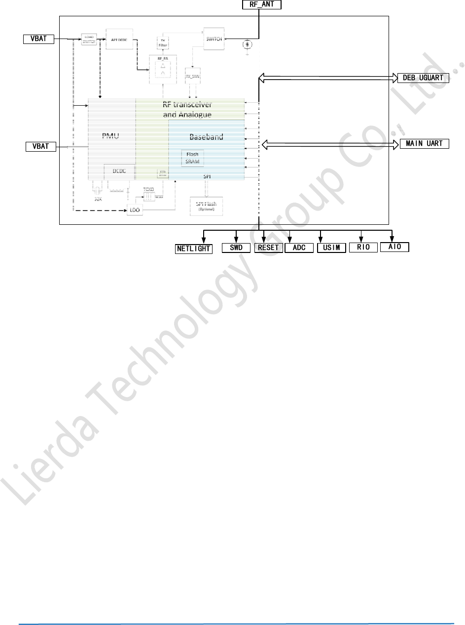
4. Functional Diagram
The block diagram below shows the main features of the NBXX-01: radio frequency, power
management, peripheral interface.
Figure 1 Module feature Illustration
5. Functions
5.1 Overview
The NB-IoT Module has 42 SMT pins in total, this chapter below will give more information:
Power Supply
Gate-Limit Interface
UART Interface
USIM Interface
ADC Interface
RFID Interface
NETLIGHT
第6页共17页
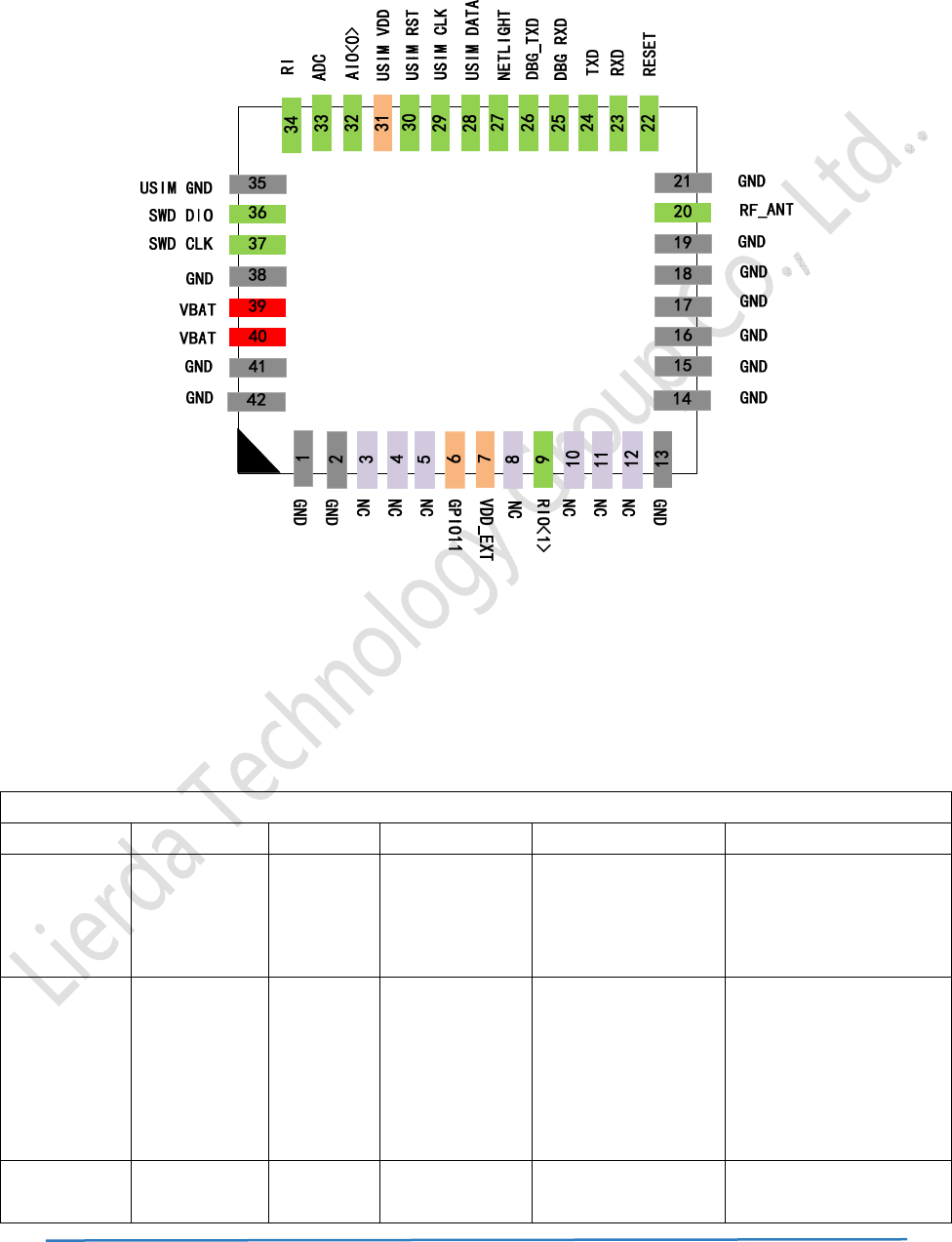
6. Pin definition
Figure 2 NBXX-01 Module Pins Illustration
6.1 Description of pins
The definition and description of Module NBXX-01`s pins is below:
Pin description:
Power Supply pins:
Name Number Attribute Description DC characteristics Remarks
VBAT 39,40 PI Main Power
Module
VBAT=3.1V~4
.2V
Vmax=4.2V
Vmin=3.1V
Vnorm=3.6V
VDD_EXT 7 PO Provide 3
Voltage for
external
circuit
Vnorm=3.0V
IOmax=20mA
If this will never be
needed, keep open. If
this will be used, we
recommend adding a
2.2 ~ 4.7 uF bypass
capacitor
GND 1,2,13~19,
21,38,41~42
Ground
第7页共17页
SWD Interface
SWD_IO 36 IO Serial line
data signal
VOLmax=0.4V
VOHmin=2.4V
VILmin=-0.3V
VILmax=0.6V
VIHmin=2.1V
VIHmax=3.3V
This interface is
designed to firmware
programming. Using
this interface to
program firmware will
reset the IEMI No. It
requires UART
Update Program to
protect IMEI No.
during program/
Update.
SWD_CLK 37 DI Serial line
clock signal
VOLmax=0.4V
VOHmin=2.4V
Reset Pin
RESET 22 DI Reset the
module
RPU≈78kΩ
VIHmax=3.3V
VIHmin=2.1V
VILmax=0.6V
Internal Up-adjust,low
voltage when active.
Simulate I/O Interface
RIO<1> 9 AIO Simulation Not Active yet. Keep
clear.
AIO<0> 32 AIO Simulation Not Active yet. Keep
clear.
Network status indicate port
NETLIGHT 27 DO Network
status
indicator
VOLmax=0.4V
VOHmin=2.4V
Not Active yet. Keep
clear.
ADC Interface
ADC 33 AI General
Simulation-Di
gital Signal
transform
Not Active yet. Keep
clear.
Main UART Communication Interface
RXD 23 DI Receive data. VILmax=0.6V
VIHmin=2.1V
VIHmax=3.3V
Keep Voltage under
3.0V, If not Active yet.
Keep clear.
TXD 24 DO Send data. VOLmax=0.4V
VOHmin=2.4V
Keep Voltage under
3.0V, If not Active yet.
Keep clear.
RI 34 DO Signal
Indicate
VOLmax=0.4V
VOHmin=2.4V
Keep Voltage under
3.0V, If not Active yet.
Keep clear.
Emulation Port
DBG_RXD 25 DI Receive data. VILmax=0.6V
VIHmin=2.1V
If not Active yet. Keep
clear.
第8页共17页
VIHmax=3.3V
DBG_TXD 26 DO Send data. VOLmax=0.4V
VOHmin=2.4V
If not Active yet. Keep
clear.
USIM Interface
USIM_VDD 31 DO Provide power
supply for
USIM Card
Vnorm=3.0V All signals go through
USIM Interface should
be ESD protected by
TSD diode.
USIM_RST 30 DO USIM Reset
terminal
VOLmax=0.4V
VOHmin=2.4V
USIM_DAT
A
28 IO USIM Data
terminal
VOLmax=0.4V
VOHmin=2.4V
VILmin=-0.3V
VILmax=0.6V
VIHmin=2.1V
VIHmax=3.3V
USIM_CLK 29 DO USIM clock
terminal
VOLmax=0.4V
VOHmin=2.4V
USIM_GND 35 USIM ground Share ground
RF Interface
RF_ANT 20 IO RF antenna
interface
Impedance is 50Ω
Reserved pins
GPIO11 6 IO If not Active yet. Keep
clear.
NC 3~5,8,
10~12
Reserved Not connect to any
other pins (Temp)
6.2 Operating mode
The NBXX-01 module has three modes of operation to determine the different levels of low
power consumption based on usage scenarios. Under normal operating conditions are divided
into:
Active mode The module is active; all functions are normally available for
data transmission and reception; the module can switch to Idle
mode or PSM mode in this mode.
Idle The module is in a light sleep state, the module is in a network
connection state and can accept paging messages. In this
mode, the module can be switched to active mode or PSM
mode.
PSM Module only RTC work, the module is in the network is not
connected, no longer accept paging messages. When DTE
(Data Terminal Equipment) actively send data or timer T3412
(periodic update) timeout, the module will be awakened.
6.
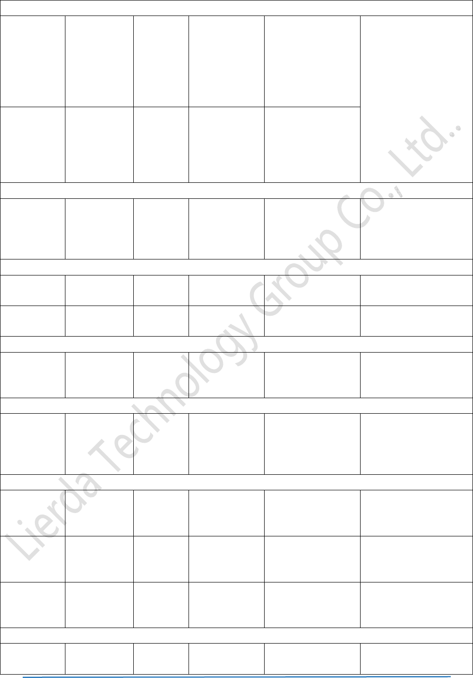
3
Th
e
doe
Th
e
po
w
For
cer
a
Th
e
mo
d
the
Th
e
upd
3
Powe
r
e
NBXX-01
m
s not drop
b
e
performan
c
w
er supply
m
better perf
o
a
mic capaci
t
e
maximum
c
d
ule power
c
power cons
模块
不
电
流
e
process
o
ate and ne
t
r
supply
m
odule's po
w
b
elow 3.1V. I
c
e of the
m
m
odule is ve
r
o
rmance, it
t
ors 100nf,
1
F
c
onsumptio
n
c
onsumptio
n
umption di
a
TX
RX
不
活动定时器
o
f module i
n
t
work (TAU
)
第
& pow
e
w
er supply
r
f the suppl
y
m
odule dep
e
r
y importan
t
is recomm
1
00pf and 2
2
igure 3 Ref
e
n
of module
s
n
and exten
a
gram of mo
Idle
T3324
n
to the PS
M
)
, module
w
第
9
页共17
e
r savin
g
r
ange is 3.1
y
voltage is l
o
e
nds largel
y
t
, in which t
h
ended to p
2
pf near V
B
e
rence desi
g
s
under PS
M
d battery p
o
dules in diff
e
M
as follo
w
w
ill apply to
页
g
techn
o
V to 4.2 V,
m
o
wer than 3
.
y
on the po
w
h
e power su
lace a 100
u
B
AT. The ref
e
g
n for powe
r
M
is 5uA.P
S
o
wer supply
e
rent mode
s
PSM
T3412
w
s: to mak
e
the reques
t
o
logy
m
aking sur
e
.
1 V, the mo
w
er supply,
pply curren
t
u
F tantalu
m
e
rence circ
u
r
supply
S
M, the mai
n
time. The
f
s
.
T
e
a connec
t
t
message,
e
that the in
p
dule will be
so the de
s
t
of at least
0
m
capacitor
u
it is shown
b
n
purpose is
f
ollowing fig
u
Idle
T
AU
t
ion or tra
c
the netwo
r
p
ut voltage
abnormal.
s
ign of the
0
.5A.
and three
b
elow。
to reduce
u
re shows
c
king a
r
ea
r
k terminal
res
p
tim
e
for
n
Wh
e
for
t
TA
U
Th
e
oth
e
Po
w
pin,
Po
w
sup
NB
X
rec
o
p
onse mess
e
r. When th
e
n
etworking
o
e
n the mod
u
t
he cell me
s
U
updates)
c
e
re are two
w
e
r is when t
h
w
er supply
m
and the se
q
w
er off mo
d
ply of the V
B
X
X-01 mod
u
o
mmended
c
age back t
o
e
T3324 tim
e
o
r public da
t
u
le is in the
P
s
sage, the c
c
ontinue to
w
w
ays for mo
d
h
e T3412 ti
m
m
ode: This
m
q
uence dia
g
d
e: This m
o
B
AT pin. Th
e
Fi
g
u
le reset: th
e
c
ircuit can
o
第
o
the config
u
e
r expires,
m
t
a network i
n
P
SM mode,
ell reelectio
w
ork.
d
ules to qui
t
m
er goes ou
m
odule can
g
ram is as f
o
Figur
e
o
dule can
a
e
se sequen
c
g
ure 5 Turn
e
module c
a
o
utput a low
第
10
页共
1
u
ration of th
e
m
odule will
e
n
itialization,
the networ
k
n, etc. But t
t
PSM mod
e
t, the TAU
s
automatical
o
llows:
e
4 power o
a
utomaticall
y
c
e diagram
off the po
w
a
n reset to
a
level throu
g
1
7页
e
T3324 nu
m
e
nter the PS
cannot app
k
activities
w
he T3412 ti
e
: one way i
s
s
tarts, the m
o
ly start wor
k
n sequenc
e
y
stop wor
k
is as follow
s
w
er supply
s
a
low level
o
g
h registers
o
m
erical time
r
M. module
f
ly for entry i
w
ill be close
d
mer will (as
s
DTE send
s
o
dule exits
P
k
ing by pow
e
e
k
ing by dis
c
s
:
s
equence
o
f reset pin
f
o
r mechani
c
r
module, a
n
f
or emergen
i
nto the PS
M
d
, including
t
sociated wi
t
s
the data a
c
P
SM.
e
r supply to
c
onnecting
t
f
or a certain
c
al switche
s
n
d start up
cy service
M
.
t
he search
t
h periodic
c
tively, the
the VBAT
t
he power
time. The
s
.
6.
4
Th
e
Mai
TX
D
RX
D
RI:
i
Th
e
960
De
b
DB
G
DB
G
Th
e
soft
w
4
UART
e
NBXX-01
m
n communi
c
D
: send the
d
D
: accept th
e
i
ndicate the
e
main com
m
0bps.
b
ug port:
G
_TXD: se
n
G
_RXD: rec
e
debug por
w
are, and t
h
Figure 6 R
Joggle
m
odule has
c
ation port:
d
ata and lin
k
e
the data, l
signal side,
m
unication
p
n
d data to th
eive data fr
o
t can be u
s
h
e baud rat
e
M
o
M
第
eset circuit
two UART
p
k
to the bot
t
ink with the
link to the
b
p
ort is tran
s
e COM por
t
o
m the CO
M
s
ed to view
e
is 921600
b
TXD
RXD
RI
GND
o
dule (DCE)
M
ain port
Figure7 S
e
第
11
页共
1
(left MCU I
p
orts: main
p
t
om MCU
bottom MC
b
ottom MC
U
s
mitted thro
t
of the host
M
port of the
the syste
m
b
ps.
e
rial circuit
r
1
7页
O driver, ri
g
p
ort and de
b
U
U
ugh the AT
compute
r
upper com
p
m
log throug
TXD
RXD
RI
GND
Mot
Ser
r
eference d
e
g
ht button
d
b
ug port.
command,
p
uter
h the PC s
o
herboar
d
(DTE)
ial port
e
sign
d
river)
and the b
a
o
ftware UE
a
ud rate is
Log View
Ser
i
6.
5
NB
X
app
sup
(1)
I
foll
o
(2)
T
mu
c
(3)
T
i
al port appl
5
USIM
X
X-01's ESI
lication too
l
ports 3 V U
S
I
n order to i
m
o
w the stan
d
T
he USIM
s
c
h less than
T
he USIM s
Mo
d
M
Figu
ication desi
g
M
o
Figure
9
card in
t
M and USI
M
l
s. On the
S
IM card. 6
F
m
prove the
d
ard design
s
lot is as cl
o
200mm as
ignal is far
a
第
DBG TXD
DBG RXD
GND
d
ule (DCE)
M
ain port
re 8 Debug
g
g
n: the desi
g
TXD
RXD
RI
GND
o
dule (DCE)
Main port
9
Referenc
e
t
erface
M
interface
s
module, th
e
pin USIM c
a
F
igure 10
U
reliability a
n
in the USI
M
o
se to the
m
possible.
a
way from t
h
第
12
页共
1
g
ing serial
c
g
n of 3.3V
s
1K
1K
1K
1K
e
design of
s
s
upports 3
G
e
re is a U
S
a
rd circuit i
s
U
SIM card c
n
d availabili
t
M
circuit desi
m
odule as p
o
h
e RF and
V
1
7页
TXD
RXD
GND
P
C
Se
r
c
ircuit refere
n
s
ystem is as
TXD
RXD
RI
GND
Mot
h
(
Ser
i
s
erial voltag
e
G
PP specific
S
IM interfa
c
s
designed
a
ircuit desig
n
t
y of the US
gn.
o
ssible, an
d
V
BAT circuit
s
C
(DTE)
r
ial por
t
n
ce design
follows:
h
erboar
d
(
DTE)
i
al por
t
e
matching
ation, whic
h
c
e monitori
n
a
s follows,
n
referenc
e
IM card in t
h
d
the length
s
.
circuit
h
is suitable
n
g circuit,
w
e
h
e applicati
o
of the wal
k
for routine
w
hich only
o
n. Please
k
line is as
(4)
wid
e
USI
cro
s
the
m
(5)
I
USI
USI
ES
D
(6)
sup
6.
6
stat
Sta
n
SM
S
UR
C
6.
7
Th
e
stat
e
Sta
t
LO
W
HI
G
Ensure tha
t
e
. The widt
h
M_VDD is
a
s
stalk betw
e
m
from the
e
I
n order to
o
M card slot,
M card slo
t
D
protection
The RF b
y
pression.
6
RI ti
m
us
n
dby
S
C
7
Net
w
e
network s
t
e
is listed in
t
us
M
W
T
G
H
T
The refer
e
t
the groun
d
h
of the grou
a
dded nea
r
e
en USIM_
D
e
ncircling gr
o
o
ffer good
E
ensure the
t
between
2
. Attention,
t
y
pass cap
a
m
e ser
RI respo
HIGH
When a
become
s
Some U
R
Figu
w
ork S
t
t
atus indica
t
the lower t
a
M
odule Fun
T
he module
T
he module
e
nce circuit
第
d
connectio
n
nd wire is n
r
the USIM
D
ATA and U
o
und.
E
SD protecti
o
USIM interf
a
2
2 series re
s
t
he USIM p
e
a
citor (33p
F
ies sta
t
nse
SMS signa
l
s
HIGH stat
e
R
C signals
c
re 11 RI st
a
t
atus In
t
ion signal
c
a
ble.
ction
does not w
synchroniz
e
is designe
d
第
13
页共
1
n
between
t
o less than
slot to add
SIM_CLK.
K
o
n, add a T
V
a
ce module
s
istor to re
s
e
ripheral cir
c
F
) is place
d
t
e (und
l
is receive
d
e
after abou
c
an start RI
a
tus when r
e
dicatio
c
an be indi
c
ork or sync
h
e
with the n
e
d
as follows
:
1
7页
t
he module
0.5mm, so
a
a less tha
n
K
eep them
a
V
S diode a
r
is not dam
a
s
train stray
c
uit should
c
d
near the
er dev
e
d
, RI becom
t 120ms
to keep the
e
ceiving U
R
n(und
e
c
ated by th
e
h
ronize with
e
twork
:
and USIM
c
a
s to maint
a
n
1uF deco
u
a
way from
e
r
ray. The T
V
a
ged by ES
D
EMI trans
m
c
lose to the
USIM slot
e
lopm
e
es LOW, a
n
120ms low
R
C or SMS
e
r deve
l
e
LED lamp
the networ
k
c
ard slot is
a
in the sam
e
u
pling capa
c
e
ach other
a
V
S pipe is cl
D
. In the
m
m
ission and
USIM card
c
to improv
e
e
nt)
n
d the state
level
l
opme
n
, and the p
i
k
short and
e
potential.
c
itor.Avoid
a
nd shield
ose to the
m
odule and
enhanced
c
onnector.
e
the EMI
of LOW
n
t)
i
n working
6.
8
RF
c
Th
e
bot
h
par
t
of t
h
atte
50
o
6.
9
RT
O
Fre
q
900
850
8
RF
C
c
ircuit desi
g
e
NBXX-01
m
h
sides of s
o
t
. In addition
h
e radio fre
q
ntion to the
o
hms in the
9
RF O
O
utput Po
w
q
uency
MHz
MHz
Figure
C
ircuit
D
g
n referenc
e
m
odule prov
o
me ground
,
, there is a
π
q
uency, it is
module RF
design of R
utput
P
w
e
r
第
12 Refere
n
D
esign
e
is as follo
w
Figur
e
ides an ant
e
,
and the pu
π
capacitor
t
better to p
u
pin and ch
a
F PCB.
P
ower
Max
23dB
m
23dB
m
第
14
页共
1
n
ce design
o
w
s:
e
13 RF Ci
r
e
nna conne
c
rpose is to
p
t
hat matche
u
t the capa
c
a
racteristic i
m
m
±2dB
m
±2dB
1
7页
o
f network
i
r
cuit Desig
n
c
ted with th
e
p
rovide a b
e
s the circuit
c
itor close t
o
m
pedance
o
i
ndicator la
m
n
e
RF pads i
n
e
tter ground
used to reg
u
o
RF_ANT
p
o
f RF anten
n
m
p
n
the anten
n
connection
ulate the pe
p
in of the m
o
n
a pin shoul
d
n
a pads on
for the RF
rformance
o
dule. Pay
d
be set at
第15页共17页
RF Sensitivity
Frequency Sensitivity
900MHz -128dBm
850MHz -128dBm
Service Frequency
Frequency Receiving Frequency Transmitting Frequency
900MHz 925~960MHz 880~915MHz
850MHz 869~894MHz 824~849MHz
6.10 Antenna Requirements
NB-IoT antenna requirements shows in the following table:
Parameter Type Requirement
Frequency Range 824-960MHz
VSWR ≤2
Gain(dBi) ≥1
Maximum Input Power(W) 5
Input matching impedance(Ω) 50
RHCP linear
7. Electrical Characteristics, Reliability
and Wireless Characteristics
The NBXX-01 module simulates the rated voltage parameters of the voltage and the digital
voltage as shown in the following table:
Parameter Min. Max. Unit
VBAT 3.1 +4.2 V
Maximum current of power supply 0 0.3 A
RMS Current 0 0.25 A
Digital pin voltage -0.3 +3.0 V
Analog pin voltage -0.3 +4.2 V
The voltage of analog / digital pins in the
state of power loss -0.25 +0.25 V
Working Temperature:
Parameter Min. Typ. Max. Unit
Operating Temperature Range (OTR) -30 +25 +85 ℃
Storage Temperature Range -40 +125 ℃
第16页共17页
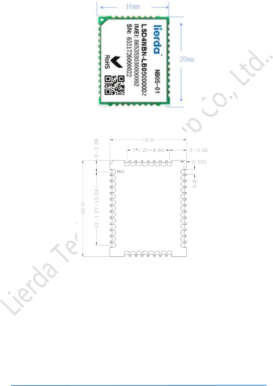
8. Appearance and Structure
Figure 14 Appearance Size
Figure 15 Encapsulation Dimension Figure and Unit (mm)
9. Contact Us
Company Address:Lierda IOT Technology Park, Wenyi West Road No. 1326, Hangzhou
Contact Number:0571-88800000;
Contact Email:NBIoT_support@lierda.com
Official Website:Http://www.lierda.com
The NB05-01 module is designed to comply with FCC statement.FCC ID is 2AOFDNB05-01.

第17页共17页
FCCRFExposureRequirements
ThisdevicecomplieswithFCCRFradiationexposurelimitssetforthforanuncontrolledenvironment.
Theantenna(s)usedforthistransmittermustnotbeco‐locatedoroperatinginconjunctionwithany
otherantennaortransmitterandmustbeinstalledtoprovideaseparationdistanceofatleast20cm
fromallpersons.
FCCRegulations
Thisdevicecomplieswithpart15oftheFCCRules.Operationissubjecttothefollowingtwoconditions:
(1)Thisdevicemaynotcauseharmfulinterference,and(2)thisdevicemustacceptanyinterference
received,includinginterferencethatmaycauseundesiredoperation.
ThisdevicehasbeentestedandfoundtocomplywiththelimitsforaClassBdigitaldevice,pursuantto
Part15oftheFCCRules.
Theselimitsaredesignedtoprovidereasonableprotectionagainstharmfulinterferenceinaresidential
installation.Thisequipmentgenerates,usesandcanradiateradiofrequencyenergyand,ifnotinstalled
andusedinaccordancewiththeinstructions,maycauseharmfulinterferencetoradio
communications.