dresden elektronik ingenieurtechnik ARM715A02 915MHz 802.15.4 radio module User Manual deRFarm7 V1 1
dresden elektronik ingenieurtechnik gmbh 915MHz 802.15.4 radio module User Manual deRFarm7 V1 1
Users Manual
User Manual
Radio Modules
deRFarm7-15A00 / 15A02
deRFarm7-25A00 / 25A02
deRFarm7-15C00 / 15C02
deRFarm7-25C00 / 25C02
Document Version V1.1
2011-10-21

User Manual
Version 1.1
2011-10-21
Radio modules deRFarm7
dresden elektronik
ingenieurtechnik gmbh
Enno-Heidebroek-Str. 12
01237 Dresden / Germany
Tel.: +49 351 – 31 85 00
Fax: +49 351 – 3 18 50 10
wireless@dresden-elektronik.de
www.dresden-elektronik.de
Page 2 of 31
Table of contents
1. Overview ......................................................................................................................... 5
2. Application ....................................................................................................................... 5
3. Features .......................................................................................................................... 6
4. Technical data ................................................................................................................. 8
5. Mechanical data ............................................................................................................ 10
5.1. Radio module (pluggable)..................................................................................... 10
5.2. Footprint receptacles ............................................................................................ 10
5.3. Radio module (solderable).................................................................................... 11
5.4. Footprint pads ...................................................................................................... 11
5.5. PCB design .......................................................................................................... 12
6. Soldering profile of deRFarm7 ....................................................................................... 13
7. Pin assignment .............................................................................................................. 14
8. Programming ................................................................................................................. 21
8.1. Required hardware ............................................................................................... 21
8.2. JTAG interface ..................................................................................................... 22
9. Debugging and tracing .................................................................................................. 22
10. RF components ............................................................................................................. 23
10.1. deRFarm7-15A02 / 15C02 .................................................................................... 23
10.2. deRFarm7-25A00 / 25C00 .................................................................................... 23
10.3. deRFarm7-25A02 / 25C02 .................................................................................... 24
11. Radio certification .......................................................................................................... 25
11.1. United States (FCC) ............................................................................................. 25
11.2. European Union (ETSI) ........................................................................................ 26
11.3. Approved antennas .............................................................................................. 26
12. Ordering information ...................................................................................................... 28
13. Revision notes ............................................................................................................... 30
User Manual
Version 1.1
2011-10-21
Radio modules deRFarm7
dresden elektronik
ingenieurtechnik gmbh
Enno-Heidebroek-Str. 12
01237 Dresden / Germany
Tel.: +49 351 – 31 85 00
Fax: +49 351 – 3 18 50 10
wireless@dresden-elektronik.de
www.dresden-elektronik.de
Page 3 of 31
Document history
Date Version Description
2011-02-10 1.0 Initial version
2011-10-21 1.1 Addition of PCB design
Mailing list
Firm Division / Name
DE Dev. / A.Palm
Author / Check / Release
Firm Division / Name
Author DE Dev. / A.Palm
Check
release
User Manual
Version 1.1
2011-10-21
Radio modules deRFarm7
dresden elektronik
ingenieurtechnik gmbh
Enno-Heidebroek-Str. 12
01237 Dresden / Germany
Tel.: +49 351 – 31 85 00
Fax: +49 351 – 3 18 50 10
wireless@dresden-elektronik.de
www.dresden-elektronik.de
Page 4 of 31
Abbreviations
Abbreviation Description
ADC
A
nalog to
D
igital
C
onverter
BOD
B
rown
o
ut-
D
etection
CE
C
onsumer
E
lectronics
DAC
D
igital to
A
nalog
C
onverter
DBGU
D
ebug
U
nit
ETH
Eth
ernet, family of frame-based computer networking technologies for local
area networks (LAN).
EMAC
E
thernet
M
edia
A
ccess
C
ontroller
ETSI
E
uropean
T
elecommunications
S
tandards
I
nstitute
FCC
F
ederal
C
ommunications
C
ommission
GPIO
G
enerals
P
urpose
I
nput
O
utput
ISM
I
ndustrial,
S
cientific and
M
edical frequency band
JTAG
J
oint
T
est
A
ction
G
roup
ISP
I
n-
S
ystem-
P
rogramming
MAC
M
edium (
M
edia)
A
ccess
C
ontrol
MCU, µC
M
icro
c
ontroller
U
nit
PCB
P
rinted
C
ircuit
B
oard
PCBA
P
rinted
C
ircuit
B
oard
A
ssembled
PWM
P
ulse
W
idth
M
odulation
RF
R
adio
F
requency
RMII
R
educed
M
edia
I
ndependent
I
nterface
SPI
S
erial
P
eripheral
I
nterface
TWI
T
wo-
W
ire Serial
I
nterface
U[S]ART
U
niversal [
S
ynchronuous/]
A
synchronous
R
eceiver
T
ransmitter
USB
U
niversal
S
erial
B
us

User Manual
Version 1.1
2011-10-21
Radio modules deRFarm7
dresden elektronik
ingenieurtechnik gmbh
Enno-Heidebroek-Str. 12
01237 Dresden / Germany
Tel.: +49 351 – 31 85 00
Fax: +49 351 – 3 18 50 10
wireless@dresden-elektronik.de
www.dresden-elektronik.de
Page 5 of 31
1. Overview
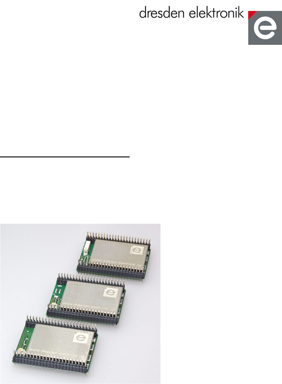
The compact designed radio modules contains a powerful ARM™7 microcontroller with 512
kBytes High-Speed Flash, On-chip USB 2.0 Full Speed Transceiver, Ethernet MAC 10/100
base-T in RMII-Mode and an onboard transceiver for 2.4 GHz or 868/915 MHz.
The 46 pin interface gives access to most hardware functions of the microcontroller.
A long radio transmission range can be achieved by using the coaxial jack (U.FL) version
with an external antenna attached. In the Sub-GHz band several hundred meters (100 m =
330 feet) can be reached without problems. The 2.4 GHz version is able to cover up to
200 m (650 feet) with a ceramic chip antenna. All versions have a 128-bit AES encryption
unit installed.
The 512 kB Flash and 128 kB RAM of the deRFarm7 modules provide enough resources to
be used for any tasks within a wireless sensor network.
2. Application
The main applications for the deRFarm7 radio modules are:
• 2.4GHz IEEE 802.15.4
• 868MHz / 915MHz IEEE 802.15.4
• ZigBee
®
Pro
• ZigBee
®
RF4CE
• ZigBee
®
IP
• 6LoWPAN
• Wireless Sensor Networks (WSN)
• industrial and home controlling and monitoring
• Gateway applications between IEEE 802.15.4 and other networks, e.g. Ethernet
User Manual
Version 1.1
2011-10-21
Radio modules deRFarm7
dresden elektronik
ingenieurtechnik gmbh
Enno-Heidebroek-Str. 12
01237 Dresden / Germany
Tel.: +49 351 – 31 85 00
Fax: +49 351 – 3 18 50 10
wireless@dresden-elektronik.de
www.dresden-elektronik.de
Page 6 of 31
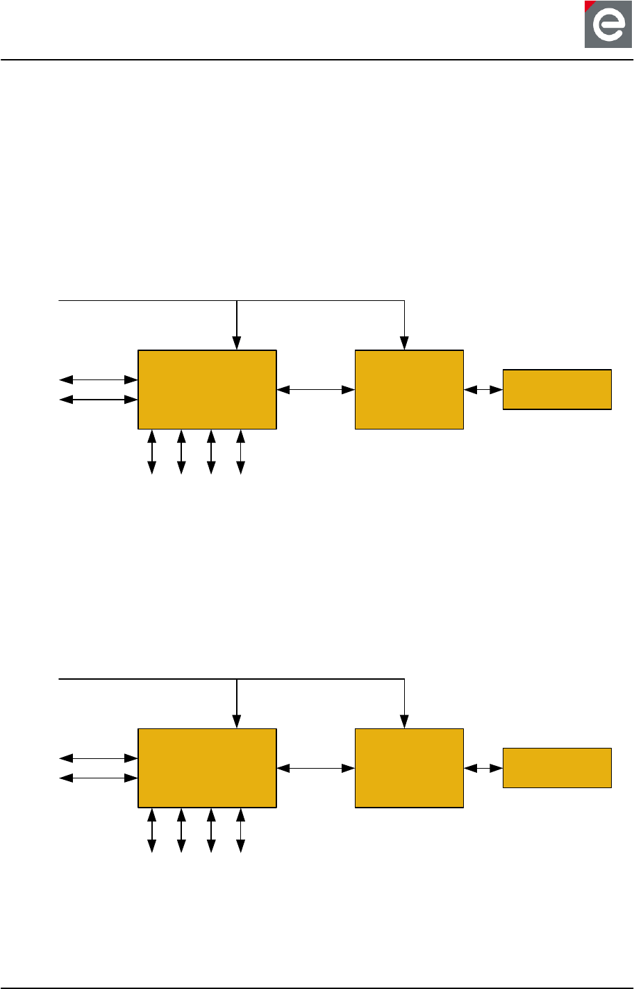
3. Features
The Sub-GHz radio modules deRFarm7-15A00 / 15C00 offer the following features:
• pluggable: 2 male connectors, 23 pins per row, 1.27mm pitch
• RF shielding
• usable signals: power supply, peripheral, programming, debugging, tracing, ADC,
GPIO, USB, Ethernet MAC
• application interfaces: 1 x UART, 1 x TWI, 1x USB, 1 x Ethernet-MAC
• Debug/Programming interfaces: 1 x SPI, 1 x JTAG
• Onboard chip-antenna and transceiver for 868/900 MHz
• Certification: FCC pending
• Compliant: CE, ETSI
AT91SAM7X512
JTAG
Chip
antenna
DBGU
3.0...3.6V
AT86RF212
SPI
VCC
UART
USB
ETH
TWI
Figure 1: block diagram deRFarm7-15A00 / 15C00
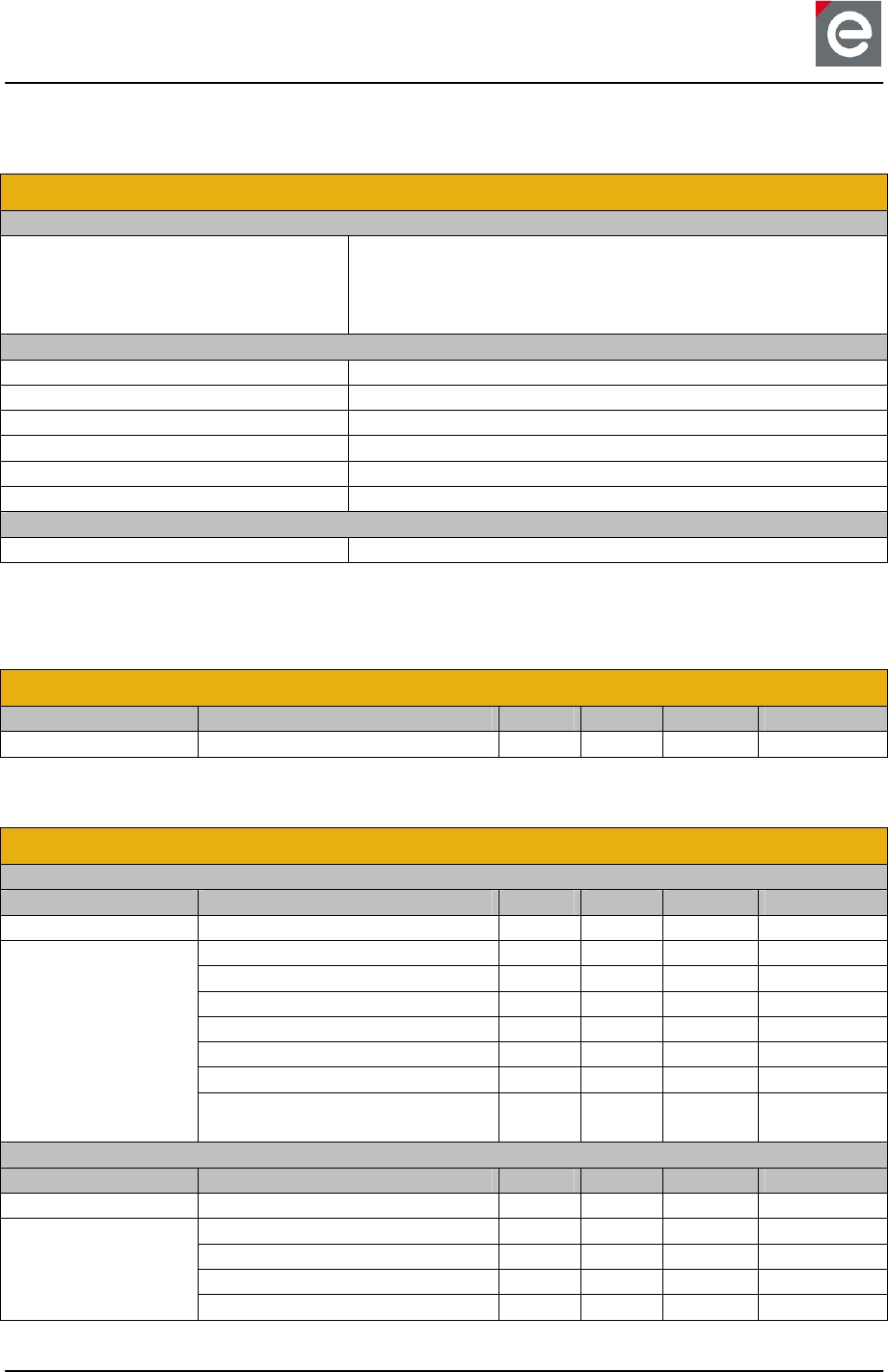
The radio modules deRFarm7-15A02 / 15C02 offer the same features like the
deRFarm7-15A00 / 15C00 except the onboard Sub-GHz chip antenna is replaced by an
U.FL coaxial receptacle for connecting an external antenna.
AT91SAM7X512
JTAG
Coaxial
Connector
DBGU
3.0...3.6V
AT86RF212
SPI
VCC
UART
USB
ETH
TWI
Figure 2: block diagram deRFarm7-15A02 / 15C02
User Manual
Version 1.1
2011-10-21
Radio modules deRFarm7
dresden elektronik
ingenieurtechnik gmbh
Enno-Heidebroek-Str. 12
01237 Dresden / Germany
Tel.: +49 351 – 31 85 00
Fax: +49 351 – 3 18 50 10
wireless@dresden-elektronik.de
www.dresden-elektronik.de
Page 7 of 31
The 2.4 GHz radio modules deRFarm7-25A00 / 25C00 offer the following features:
• compact size: 30 x 22.7 mm (for 25A00) and 30 x 20.4 mm (for 25C00)
• pluggable: 2 male connectors, 23 pins per row, 1.27mm pitch
• RF shielding
• usable signals: power supply, peripheral, programming, debugging, tracing, ADC,
GPIO, USB, Ethernet MAC
• application interfaces: 1 x UART, 1 x TWI, 1x USB, 1 x Eth-MAC
• Debug/Programming interfaces: 1 x SPI, 1 x JTAG
• Onboard chip-antenna and transceiver for 2.4 GHz
• Certification: FCC pending
• Compliant: CE, ETSI
AT91SAM7X512
JTAG
Chip
antenna
DBGU
3.0...3.6V
AT86RF231
SPI
VCC
UART
USB
ETH
TWI
Figure 3: block diagram deRFarm7-25A00 / 25C00
The radio modules deRFarm7-25A02 / 25C02 offer the same features like the
deRFarm7-25A00 / 25C00 except the onboard 2.4 GHz chip antenna is replaced by an U.FL
coaxial receptacle for connecting an external antenna.
AT91SAM7X512
JTAG
Coaxial
Connector
DBGU
3.0...3.6V
AT86RF231
SPI
VCC
UART
USB
ETH
TWI
Figure 4: block diagram deRFarm7-25A02 / 25C02
User Manual
Version 1.1
2011-10-21
Radio modules deRFarm7
dresden elektronik
ingenieurtechnik gmbh
Enno-Heidebroek-Str. 12
01237 Dresden / Germany
Tel.: +49 351 – 31 85 00
Fax: +49 351 – 3 18 50 10
wireless@dresden-elektronik.de
www.dresden-elektronik.de
Page 8 of 31
4. Technical data
Table 1: Mechanical data
Mechanical
Radio modules
Size (L x W x H) 30 x 22.7 x 8.2 mm
1
(for deRFarm7-15A02 / 25A00 / 25A02)
30 x 20.4 x 4.3 mm
(for deRFarm7-15C02 / 25C00 / 25C02)
Connectors
number of headers 2
pins per header 23
pitch 1.27 mm
pin length 3.05 mm
pin diameter 0.51 mm
Insulator (L x W x H) 29.2 x 2.5 x 2.5 mm
Pins
pitch 1.27 mm
1
unplugged radio module
Table 2: Temperature range
Temperature range
Min Typ Max Unit
Working range T_work -40 +85 °C
Table 3: Electrical data
Electrical (Vcc = 3.3VDC)
deRFarm7-15A02 / 15C02
Parameter Min Typ Max Unit
Supply Voltage VCC 3.0 3.3 3.6 VDC
Current
consumption
I_TXon (TX_PWR = +10 dBm)
52 mA
I_TXon (TX_PWR = +5 dBm) 46 mA
I_TXon (TX_PWR = 0 dBm) 43 mA
I_RXon 36 mA
I_Idle (Txoff, BOD on) TBD mA
I_BODon TBD µA
I_Sleep
(depends on Sleep Mode)
TBD TBD TBD µA
deRFarm7-25A00 / 25A02 / 25C00 / 25C02
Parameter Min Typ Max Unit
Supply Voltage VCC 3.0 3.3 3.6 VDC
Current
consumption
I_TXon (TX_PWR = +3 dBm) 13 mA
I_TXon (TX_PWR = +1 dBm) 12 mA
I_TXon (TX_PWR = -17 dBm) 7.5 mA
I_RXon TBD mA
User Manual
Version 1.1
2011-10-21
Radio modules deRFarm7
dresden elektronik
ingenieurtechnik gmbh
Enno-Heidebroek-Str. 12
01237 Dresden / Germany
Tel.: +49 351 – 31 85 00
Fax: +49 351 – 3 18 50 10
wireless@dresden-elektronik.de
www.dresden-elektronik.de
Page 9 of 31
I_Idle (Txoff, BOD on) TBD mA
I_BODon TBD µA
I_Sleep
(depends on Sleep Mode)
TBD TBD TBD µA
Table 4: Radio transmission data
Radio (Vcc = 3.3VDC)
deRFarm7-15A02 / 15C02
Parameter Value Unit
Frequency range Channel 0 (EU) 868.3 MHz
Frequency range Channel 1…10 (US) 906…924 MHz
Parameter Min Typ Max Unit
Transmitting
power conducted
Channel 0; 20kBit/sec
TX_PWR = +5dBm
5.0 dBm
Transmitting
power conducted
Channel 1…10; 40kBit/sec
TX_PWR = +10dBm
8.5 dBm
deRFarm7-25A00 / 25A02 / 25C00 / 25C02
Parameter Value Unit
Frequency range Channel 11…26 (EU) 2405…2480 MHz
Parameter Min Typ Max Unit
Transmitting
power conducted
Channel 11…26; 250kBit/sec
TX_PWR = +3dBm
3.0 dBm
User Manual
Version 1.1
2011-10-21
Radio modules deRFarm7
dresden elektronik
ingenieurtechnik gmbh
Enno-Heidebroek-Str. 12
01237 Dresden / Germany
Tel.: +49 351 – 31 85 00
Fax: +49 351 – 3 18 50 10
wireless@dresden-elektronik.de
www.dresden-elektronik.de
Page 10 of 31
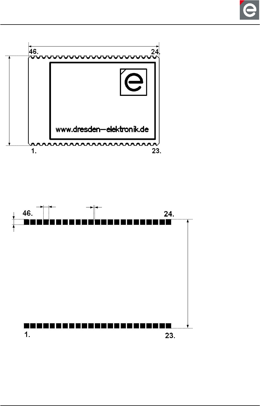
5. Mechanical data
5.1. Radio module (pluggable)
Used connectors: SAMTEC “TMS-123-02-L-S”
22,7mm
30,0mm
Figure 5: Size deRFarm7-15A02 / 25A00 / 25A02
5.2. Footprint receptacles
Used receptacles: SAMTEC “SLM-123-01-L-S”
20,4mm
0,65mm1,27mm
Figure 6: Footprint receptacles 1.27mm pitch
User Manual
Version 1.1
2011-10-21
Radio modules deRFarm7
dresden elektronik
ingenieurtechnik gmbh
Enno-Heidebroek-Str. 12
01237 Dresden / Germany
Tel.: +49 351 – 31 85 00
Fax: +49 351 – 3 18 50 10
wireless@dresden-elektronik.de
www.dresden-elektronik.de
Page 11 of 31
5.3. Radio module (solderable)
20.4mm
30,0mm
Figure 7: Size deRFarm7-15C02 / 25C00 / 25C02
5.4. Footprint pads
21.4mm
1.0mm
1.0mm
0.27mm
Figure 8: Footprint for deRFarm7-15C02 / 25C00 / 25C02
User Manual
Version 1.1
2011-10-21
Radio modules deRFarm7
dresden elektronik
ingenieurtechnik gmbh
Enno-Heidebroek-Str. 12
01237 Dresden / Germany
Tel.: +49 351 – 31 85 00
Fax: +49 351 – 3 18 50 10
wireless@dresden-elektronik.de
www.dresden-elektronik.de
Page 12 of 31
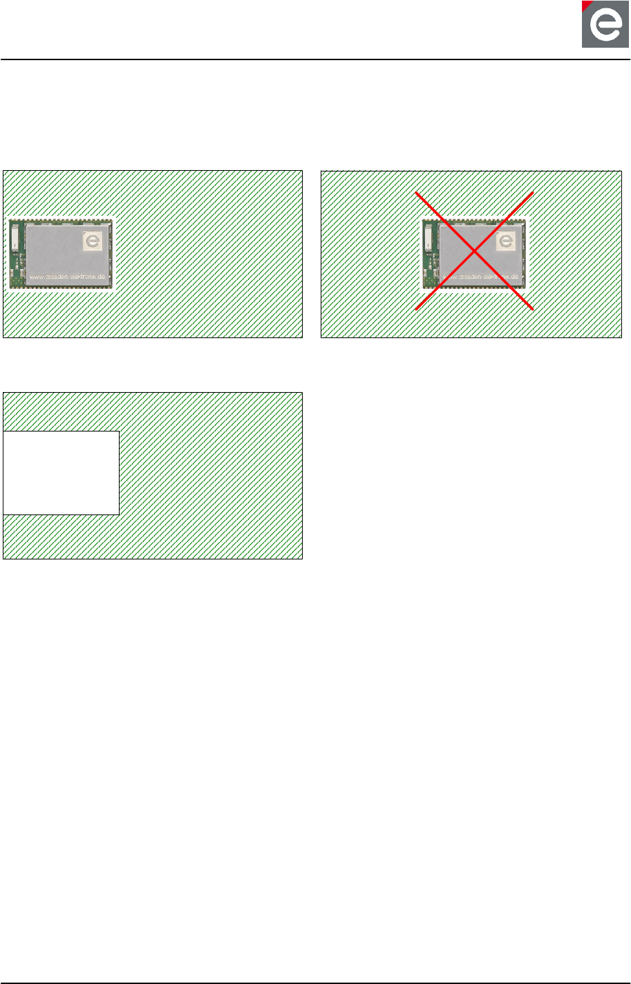
5.5. PCB design
The PCB design of the radio module base board and placement affects the radio characteris-
tic. The radio module should be placed at the edge or side of a base board. The chip anten-
na should be directed to PCB side.
PCB
OK
PCB
Do not place ground areas below the radio module and near the chip-antenna.
PCB
No Ground
Plane
If the base board with the radio module will be placed into a metal case, it is necessary to
use the radio module variant with coaxial connector and an external antenna.
User Manual
Version 1.1
2011-10-21
Radio modules deRFarm7
dresden elektronik
ingenieurtechnik gmbh
Enno-Heidebroek-Str. 12
01237 Dresden / Germany
Tel.: +49 351 – 31 85 00
Fax: +49 351 – 3 18 50 10
wireless@dresden-elektronik.de
www.dresden-elektronik.de
Page 13 of 31
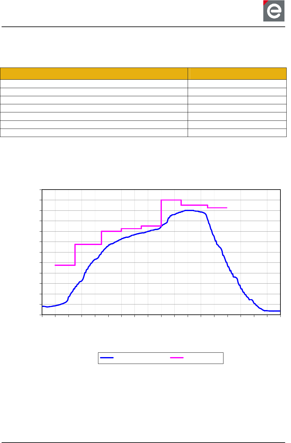
6. Soldering profile of deRFarm7
Table 5 gives the soldering profile for the radio modules.
Table 5: Soldering Profile
Profile Feature Values
Average-Ramp-up Rate (217°C to Peak) 3°C/sec max.
Preheat Temperature 175°C ±25°C 120 sec. max
Temperature Maintained Above 217°C 60 sec.
Time within 5°C of Actual Peak Temperature 20 sec. to 40 sec.
Peak Temperature Range 260°
Ramp-down Rate 6°C/sec max.
Time 25°C to Peak Temperature 8 min. max.
Figure 9 shows a recorded soldering profile for a radio module. The blue colored line illus-
trates a temperature sensor placed next to the soldering-contacts of the radio module. The
pink line shows the set temperatures depending on the zone within the reflow soldering ma-
chine.
40
60
80
100
120
140
160
180
200
220
240
260
280
0
20
40
60
80
100
120
140
160
180
200
220
240
260
280
300
320
340
360
t [s]
T [°C]
Measured Temp. Zone Temp.
Figure 9: Recorded soldering profile
A solder process without supply of nitrogen causes a discoloration of the metal RF-shielding.
User Manual
Version 1.1
2011-10-21
Radio modules deRFarm7
dresden elektronik
ingenieurtechnik gmbh
Enno-Heidebroek-Str. 12
01237 Dresden / Germany
Tel.: +49 351 – 31 85 00
Fax: +49 351 – 3 18 50 10
wireless@dresden-elektronik.de
www.dresden-elektronik.de
Page 14 of 31
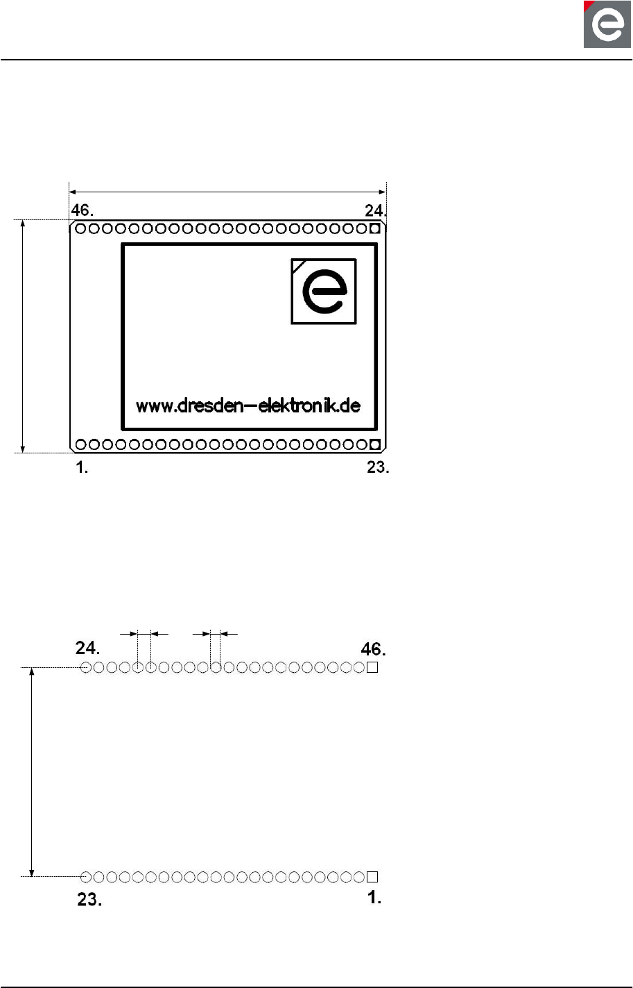
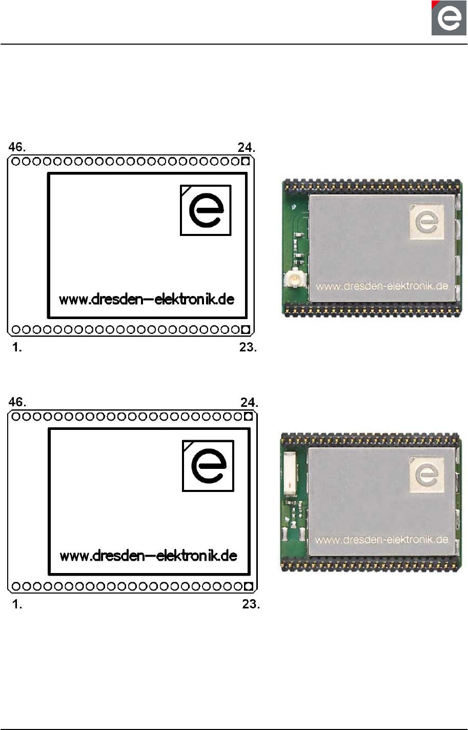
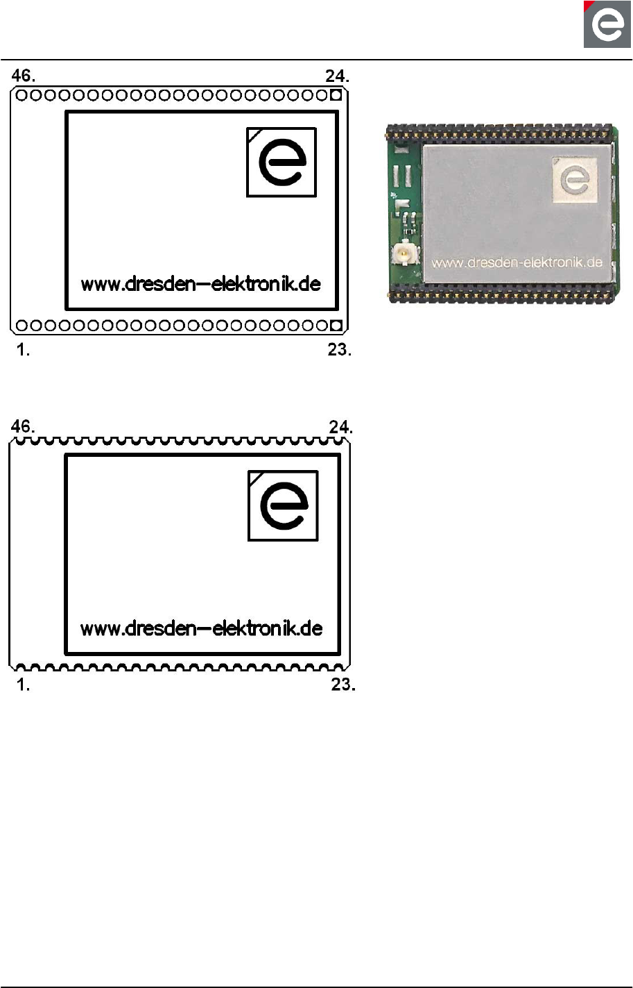
7. Pin assignment
Both pin headers respectively pin contacts provide the most important signals to the custom-
er: power supply, peripheral, programming, debugging, tracing, analog measurement and
free programmable ports. All provided signals except VCC, GND, RSTN, JTAGSEL, TDI,
TDO, TCK, TMS, USBDM, USBDP and ADVREF are free programmable port pins (GPIO).
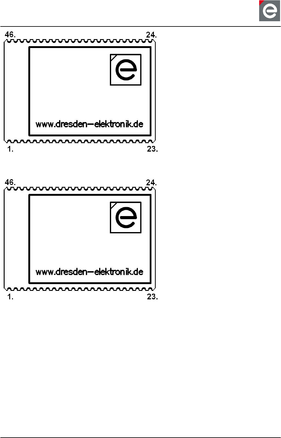
Figure 10: Top overlay deRFarm7-15A02
Figure 11: Top overlay deRFarm7-25A00
User Manual
Version 1.1
2011-10-21
Radio modules deRFarm7
dresden elektronik
ingenieurtechnik gmbh
Enno-Heidebroek-Str. 12
01237 Dresden / Germany
Tel.: +49 351 – 31 85 00
Fax: +49 351 – 3 18 50 10
wireless@dresden-elektronik.de
www.dresden-elektronik.de
Page 15 of 31
Figure 12: Top overlay deRFarm7-25A02
coming soon
Figure 13: Top overlay deRFarm7-15C02
User Manual
Version 1.1
2011-10-21
Radio modules deRFarm7
dresden elektronik
ingenieurtechnik gmbh
Enno-Heidebroek-Str. 12
01237 Dresden / Germany
Tel.: +49 351 – 31 85 00
Fax: +49 351 – 3 18 50 10
wireless@dresden-elektronik.de
www.dresden-elektronik.de
Page 16 of 31
coming soon
Figure 14: Top overlay deRFarm7-25C00
coming soon
Figure 15: Top overlay deRFarm7-25C02
User Manual
Version 1.1
2011-10-21
Radio modules deRFarm7
dresden elektronik
ingenieurtechnik gmbh
Enno-Heidebroek-Str. 12
01237 Dresden / Germany
Tel.: +49 351 – 31 85 00
Fax: +49 351 – 3 18 50 10
wireless@dresden-elektronik.de
www.dresden-elektronik.de
Page 17 of 31
Table 6: Pin assignment of deRFarm7 – radio module family
Pin assignment
Pin µC-Port Pin µC-Port
1 VCC 24 VCC
2 GND 25 GND
3 ADVREF 26 PA27/DRXD/PCK3
4 USBDM 27 PA0/RXD0
5 RSTN 28 PA28/DTXD
6 PB3/ETX1 29 PA4/CTS0
7 PA11/TWCK 30 PB9/EMDIO
8 PB26/TIOB1/RI1 31 PB21/PWM2/PCK1
9 PA10/TWD 32 USBDP
10 PA1/ TXD0 33 PB19/PWM0/TCLK1
11 PB25/TIOA1/DTR1 34 PB27/TIOA2/PWM0/AD0
12 PB2/ETX0 35 PA14/IRQ1
13 PA18/SPI0_SPCK 36 PB28/TIOB2/PWM1/AD1
14 PA3/RTS0 37 PB5/ERX0
15 PA17/SPI0_MOSI 38 TCK
16 PB0/ETXCK/EREFCK 39 PB7/ERXER
17 PA16/SPI0_MISO 40 TMS
18 PB8/EMDC 41 PB1/ETXEN
19 PB6/ERX1 42 TDO
20 PB18/EF100/ADTRG 43 JTAGSEL
21 PB15/ERXDV/ECRSDV 44 TDI
22 GND 45 GND
23 GND 46 GND
User Manual
Version 1.1
2011-10-21
Radio modules deRFarm7
dresden elektronik
ingenieurtechnik gmbh
Enno-Heidebroek-Str. 12
01237 Dresden / Germany
Tel.: +49 351 – 31 85 00
Fax: +49 351 – 3 18 50 10
wireless@dresden-elektronik.de
www.dresden-elektronik.de
Page 18 of 31
Table 7: Description of available I/O port pins
Description of available I/O port pins on header pins
I/O port pin Alternate function (signal name) Comments
PA0 RXD0
PA1 TXD0
PA3 RTS0
PA4 CTS0
PA10 TWD
PA11 TWCK
PA14 IRQ1
PA16 SPI0_MISO
PA17 SPI0_MOSI
PA18 SPI0_SPCK
PA27 DRXD PCK3
PA28 DTXD
PB0 ETXCK/EREFCK PCK0
PB1 ETXEN
PB2 ETX0
PB3 ETX1
PB5 ERX0
PB6 ERX1
PB7 ERXER
PB8 EMDC
PB9 EMDIO
PB15 ERXDV/ECRSDV
PB18 EF100 ADTRG
PB19 PWM0 TCLK1
PB21 PWM2 PCK1
PB25 TIOA1 DTR1
PB26 TIOB1 RI1
PB27 TIOA2 PWM0 AD0
PB28 TIOB2 PWM1 AD1
User Manual
Version 1.1
2011-10-21
Radio modules deRFarm7
dresden elektronik
ingenieurtechnik gmbh
Enno-Heidebroek-Str. 12
01237 Dresden / Germany
Tel.: +49 351 – 31 85 00
Fax: +49 351 – 3 18 50 10
wireless@dresden-elektronik.de
www.dresden-elektronik.de
Page 19 of 31
Table 8: Signal description list
Signal name Function Type Active
Level
Comments
Power
VCC
Voltage Regulator Power Supply
Input
Power 3.0V to 3.6V
GND Ground
JTAG
TCK Test Clock Input On-board Pull-up
TDI Test Data In Input On-board Pull-up
TDO Test Data Out Output
TMS Test Mode Select Input On-board Pull-up
JTAGSEL JTAG Selection Input On-Board Pull-down
Debug Unit
DRXD Debug Receive Data Input
DTXD Debug Transmit Data Output
Reset
RSTN Microcontroller Reset I/O Low Pull-Up resistor
Clocks, Oscillators
PCK0 - PCK3 Programmable Clock Output Output
U[S]ART
TXD0 Transmit Data I/O
RXD0 Receive Data Input
RTS0 Request To Send Output
CTS0 Clear To Send Input
DTR1 Data Terminal Ready Output
RI1 Ring Indicator Input
Timer/Counter and PWM Controller
TIOA1 – 2 I/O Line A I/O
TIOB1 – 2 I/O Line B I/O
TCLK1 External Clock Inputs Input
PWM Controller
PWM0 - 2 PWM Channels Output
Interrupt
IRQ1 External Interrupt Inputs Input
SPI
SPI0_MISO Master In / Slave Out I/O
SPI0_MOSI Master Out / Slave In I/O
SPI0_SPCK SPI Serial Clock I/O
Two-Wire-Interface
TWD Two-Wire Serial Interface Data I/O
TWCK Two-Wire Serial Interface Clock I/O
USB Device Port
USBDM USB Device Port Data - Analog
USBDP USB Device Port Data + Analog
Analog-to-Digital Converter
AD0 – AD1 Analog Inputs Analog
Digital pulled-up in-
puts at reset
User Manual
Version 1.1
2011-10-21
Radio modules deRFarm7
dresden elektronik
ingenieurtechnik gmbh
Enno-Heidebroek-Str. 12
01237 Dresden / Germany
Tel.: +49 351 – 31 85 00
Fax: +49 351 – 3 18 50 10
wireless@dresden-elektronik.de
www.dresden-elektronik.de
Page 20 of 31
Signal name Function Type Active
Level
Comments
ADTRG ADC Trigger Input
ADVREF ADC Reference Analog
Ethernet MAC 10/100 (RMII Mode)
ETXCK/
EREFCK
Reference Clock Input RMII only
ETXEN Transmit Enable Output
ETX0 – ETX1 Transmit Data Output
ERX0 – ERX1 Receive Data Input
ERXER Receive Error Input
EMDC Management Data Clock Output
EMDIO Management Data Input/Output I/O
ERXDV/
ECRSDV
Carrier Sense and Data Valid Input RMII only
EF100 Force 100 Mbits/sec. Output High RMII only
User Manual
Version 1.1
2011-10-21
Radio modules deRFarm7
dresden elektronik
ingenieurtechnik gmbh
Enno-Heidebroek-Str. 12
01237 Dresden / Germany
Tel.: +49 351 – 31 85 00
Fax: +49 351 – 3 18 50 10
wireless@dresden-elektronik.de
www.dresden-elektronik.de
Page 21 of 31
8. Programming
8.1. Required hardware
Dresden elektronik ingenieurtechnik gmbh offers the hardware components for a fast startup.
The following hardware setups are possible:
• deRFarm7 radio module
• deRFgateway or deRFnode (baseboard)
• SEGGER SAM-ICE similar programmer
For example, to exchange the firmware of an ARM-based radio module, use the Atmel SAM-
ICE JTAG Emulator and the SAM-Prog firmware updater. The programmer has to be
plugged to the baseboard which is DC- or USB-powered.
Figure 16: SAM-ICE connected with baseboard plus plugged radio module
User Manual
Version 1.1
2011-10-21
Radio modules deRFarm7
dresden elektronik
ingenieurtechnik gmbh
Enno-Heidebroek-Str. 12
01237 Dresden / Germany
Tel.: +49 351 – 31 85 00
Fax: +49 351 – 3 18 50 10
wireless@dresden-elektronik.de
www.dresden-elektronik.de
Page 22 of 31
8.2. JTAG interface
All deRFarm7 variants are programmable over JTAG interface (TDI, TDO, TCK, TMS). The
radio module contains all necessary pull-up resistors onboard. Use the pin configuration
shown in Figure 17 to connect the radio module to a suitable ARM™ programmer like the
SEGGER SAM-ICE.
Figure 17: ARM JTAG interface
9. Debugging and tracing
Debugging and tracing of the radio module is possible with the RS232-Level-Shifter. This
component is offered by dresden elektronik ingenieurtechnik gmbh. The used pin connection
to connect the radio module to a suitable debug and trace hardware is shown in Figure 18.
Figure 18: Debug interface
User Manual
Version 1.1
2011-10-21
Radio modules deRFarm7
dresden elektronik
ingenieurtechnik gmbh
Enno-Heidebroek-Str. 12
01237 Dresden / Germany
Tel.: +49 351 – 31 85 00
Fax: +49 351 – 3 18 50 10
wireless@dresden-elektronik.de
www.dresden-elektronik.de
Page 23 of 31
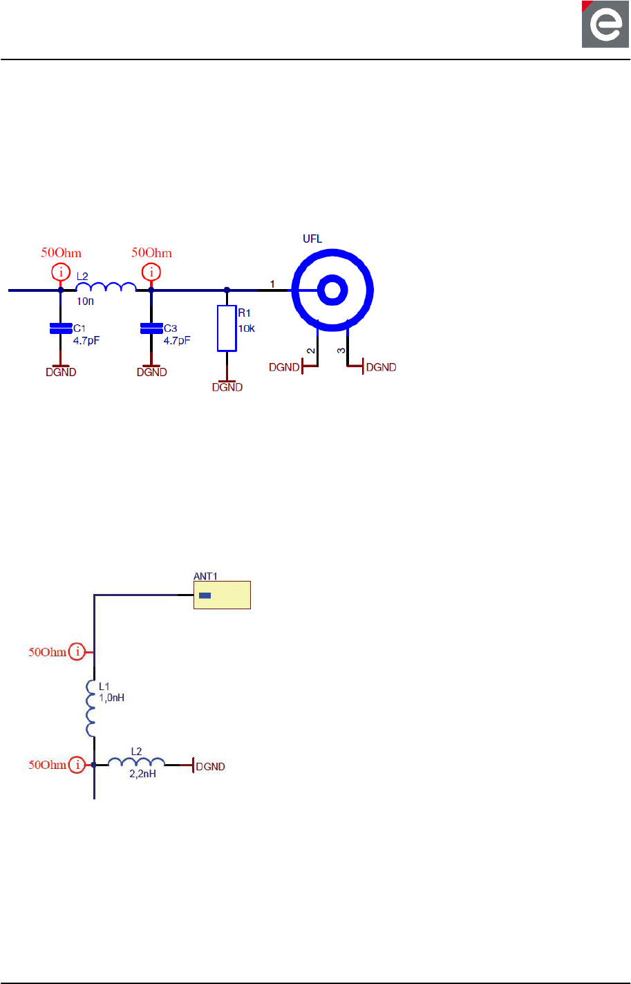
10. RF components
10.1. deRFarm7-15A02 / 15C02
The U.FL coaxial connector contains a filter network:
• L2 = 10nH (0402)
• C1 = 4.7pF (0402)
• C3 = 4.7pF (0402)
Figure 19: Filter network of deRFarm7-15A02
10.2. deRFarm7-25A00 / 25C00
The chip antenna on the deRFarm7-25A00 is matched with:
• L1 = 1.0nH (0402)
• L2 = 2.2nH (0402)
Figure 20: Matching network of deRFarm7-25A00
User Manual
Version 1.1
2011-10-21
Radio modules deRFarm7
dresden elektronik
ingenieurtechnik gmbh
Enno-Heidebroek-Str. 12
01237 Dresden / Germany
Tel.: +49 351 – 31 85 00
Fax: +49 351 – 3 18 50 10
wireless@dresden-elektronik.de
www.dresden-elektronik.de
Page 24 of 31
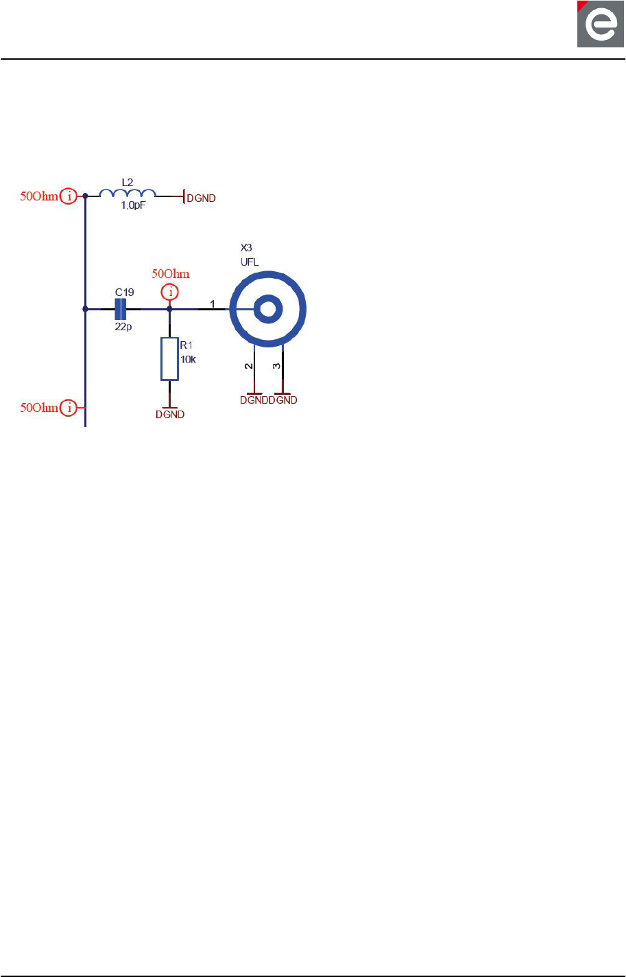
10.3. deRFarm7-25A02 / 25C02
The U.FL coaxial connector contains a filter network:
• L2 = 1.0pF (0402) (assembly variant of deRFarm7-25A00)
• C19 = 22pF (0402)
Figure 21: Matching network of deRFarm7-25A02

User Manual
Version 1.1
2011-10-21
Radio modules deRFarm7
dresden elektronik
ingenieurtechnik gmbh
Enno-Heidebroek-Str. 12
01237 Dresden / Germany
Tel.: +49 351 – 31 85 00
Fax: +49 351 – 3 18 50 10
wireless@dresden-elektronik.de
www.dresden-elektronik.de
Page 25 of 31
11. Radio certification
11.1. United States (FCC)
The deRFarm7-15A02, deRFarm7-25A00, deRFarm7-25A02, deRFarm7-15C02, deRFarm7-
25C00, deRFarm7-25C02 radio modules comply with the requirements of FCC part 15.
The FCC certification of deRFarm7-25A00, deRFarm7-25A02, deRFarm7-15C02, deR-
Farm7-25C00, deRFarm7-25C02 radio modules is pending.
To fulfill FCC Certification requirements, an OEM manufacturer must comply with the follow-
ing regulations:
The modular transmitter must be labeled with its own FCC ID number, and, if the FCC ID is
not visible when the module is installed inside another device, then the outside of the device
into which the module is installed must also display a label referring to the enclosed module.
This exterior label can use wording such as the following. Any similar wording that expresses
the same meaning may be used.
Sample label for radio module deRFarm7-15A02:
FCC
-
ID: XVV
-
ARM715A02
This device complies with Part 15 of the FCC Rules. Operation is subject to the following two
conditions: (1) this device may not cause harmful interference, and (2) this device must ac-
cept any interference received, including interference that may cause undesired operation.
To be used with the deRFarm7-15A02 modules, the external antenna have been tested and
approved which is specified in here below. The deRFarm7-15A02 modules may be integrat-
ed with other custom design antennas which OEM installer must authorize following the FCC
15.21 requirements.
The Original Equipment Manufacturer (OEM) must ensure that the OEM modular transmitter
is labeled with its own FCC ID number. This includes a clearly visible label on the outside of
the final product enclosure that displays the contents shown below. If the FCC ID is not visi-
ble when the equipment is installed inside another device, then the outside of the device into
which the equipment is installed must also display a label referring to the enclosed equip-
ment.
This equipment complies with Part 15 of the FCC Rules. Operation is subject to the following
two conditions: (1) this device may not cause harmful interference, and (2) this device must
accept any interference received, including interference that may cause undesired operation
(FCC 15.19). The internal / external antenna(s) used for this mobile transmitter must provide
a separation distance of at least 20 cm from all persons and must not be co-located or oper-
ated in conjunction with any other antenna or transmitter.
Installers must be provided with antenna installation instructions and transmitter operating
conditions for satisfying RF exposure compliance. This device is approved as a mobile de-
vice with respect to RF exposure compliance, and may only be marketed to OEM installers.
Use in portable exposure conditions (FCC 2.1093) requires separate equipment authoriza-
tion.

User Manual
Version 1.1
2011-10-21
Radio modules deRFarm7
dresden elektronik
ingenieurtechnik gmbh
Enno-Heidebroek-Str. 12
01237 Dresden / Germany
Tel.: +49 351 – 31 85 00
Fax: +49 351 – 3 18 50 10
wireless@dresden-elektronik.de
www.dresden-elektronik.de
Page 26 of 31
Modifications not expressly approved by this company could void the user's authority to
operate this equipment (FCC section 15.21).
This equipment has been tested and found to comply with the limits for a Class A digital
device, pursuant to Part 15 of the FCC Rules. These limits are designed to provide reasona-
ble protection against harmful interference when the equipment is operated in a commercial
environment. This equipment generates, uses, and can radiate radio frequency energy and,
if not installed and used in accordance with the instruction manual, may cause harmful inter-
ference to radio communications. Operation of this equipment in a residential area is likely to
cause harmful interference in which case the user will be required to correct the interference
at his own expense (FCC section 15.105).
11.2. European Union (ETSI)
The deRFarm7-15A02, deRFarm7-25A00, and deRFarm7-25A02 modules have been tested
compliant for use in European Union countries.
If the deRFarm7-15A02, deRFarm7-25A00 and deRFarm7-25A02 modules are incorporated
into a product, the manufacturer must ensure compliance of the final product to the European
harmonized EMC and low-voltage/safety standards. A Declaration of Conformity must be is-
sued for each of these standards and kept on file as described in Annex II of the R&TTE Di-
rective.
The manufacturer must maintain a copy of the deRFarm7-15A02, deRFarm7-25A00 and
deRFarm7-25A02 modules documentation and ensure the final product does not exceed the
specified power ratings, antenna specifications, and/or installation requirements as specified
in the user manual. If any of these specifications are exceeded in the final product, a submis-
sion must be made to a notified body for compliance testing to all required standards.
The “CE“ marking must be affixed to a visible location on the OEM product. The CE mark
shall consist of the initials "CE" taking the following form:
• If the CE marking is reduced or enlarged, the proportions given in the above graduat-
ed drawing must be respected.
• The CE marking must have a height of at least 5mm except where this is not possible
on account of the nature of the apparatus
• The CE marking must be affixed visibly, legibly, and indelibly.
More detailed information about CE marking requirements you can find at "DIRECTIVE
1999/5/EC OF THE EUROPEAN PARLIAMENT AND OF THE COUNCIL" on 9 March 1999
at section 12.
11.3. Approved antennas
The deRFarm7-25A00 has an integrated chip antenna. The design is fully compliant with all
regulations.
The deRFarm7-15A02 has been tested and approved for use with the antenna listed below.
The module may be integrated with other custom design antennas which OEM installer must
authorize with respective regulatory agencies. The used antenna was connected to the radio
module with a 15cm “U.FL-to-SMA pigtail”.

User Manual
Version 1.1
2011-10-21
Radio modules deRFarm7
dresden elektronik
ingenieurtechnik gmbh
Enno-Heidebroek-Str. 12
01237 Dresden / Germany
Tel.: +49 351 – 31 85 00
Fax: +49 351 – 3 18 50 10
wireless@dresden-elektronik.de
www.dresden-elektronik.de
Page 27 of 31
Table 9: Approved antenna(s) and accessory
Approved antenna(s) and accessory
Part
number
Description Manufacturer Gain
[dBi]
Min. Separation
[cm]
ANT-916-
CW-HWR-
RPS
½ wave whip antenna (915
MHz) with RP-SMA-Connector,
Antenna Factor 0 20
BN-032125 U.FL to RP-SMA pigtail,
15 cm
Hirose /
Profineon
-0,35
User Manual
Version 1.1
2011-10-21
Radio modules deRFarm7
dresden elektronik
ingenieurtechnik gmbh
Enno-Heidebroek-Str. 12
01237 Dresden / Germany
Tel.: +49 351 – 31 85 00
Fax: +49 351 – 3 18 50 10
wireless@dresden-elektronik.de
www.dresden-elektronik.de
Page 28 of 31
12. Ordering information
The product name includes the following information:
deRF xxxx - x x x xx x
Revision
Features
Size
Flash Memory
Frequency Range
Product / Chipset
Table 10: product name code
Product name code
Information Code Explanation Comments
Product / Chipset arm7 AT91SAM7X radio module
Frequency range 1 780/868/915 MHz
2 2.4 GHz
Flash memory 5 512 kByte
Size A 30 x 22.7 mm pluggable
C 30 x 20.4 mm solderable
Features
00 chip antenna onboard
02 coaxial connector onboard U.FL
Revision <blank> Rev 0
1 Rev 1
User Manual
Version 1.1
2011-10-21
Radio modules deRFarm7
dresden elektronik
ingenieurtechnik gmbh
Enno-Heidebroek-Str. 12
01237 Dresden / Germany
Tel.: +49 351 – 31 85 00
Fax: +49 351 – 3 18 50 10
wireless@dresden-elektronik.de
www.dresden-elektronik.de
Page 29 of 31
Table 11: ordering information
Ordering information
Part number Product name Comments
coming soon deRFarm7-15A00 pluggable Sub-GHz radio module with
onboard chip antenna
coming soon deRFarm7-15C00 solderable Sub-GHz radio module with
onboard chip antenna
BN-030974 deRFarm7-15A02 pluggable Sub-GHz radio module with
onboard U.FL coaxial connector
coming soon deRFarm7-15C02 solderable Sub-GHz radio module with
onboard U.FL coaxial connector
BN-027264 deRFarm7-25A00 pluggable 2.4-GHz radio module with
onboard chip antenna
coming soon deRFarm7-25C00 solderable 2.4-GHz radio module with
onboard chip antenna
BN-027265 deRFarm7-25A02 pluggable 2.4-GHz radio module with
onboard U.FL coaxial connector
coming soon deRFarm7-25C02 solderable 2.4-GHz radio module with
onboard U.FL coaxial connector

User Manual
Version 1.1
2011-10-21
Radio modules deRFarm7
dresden elektronik
ingenieurtechnik gmbh
Enno-Heidebroek-Str. 12
01237 Dresden / Germany
Tel.: +49 351 – 31 85 00
Fax: +49 351 – 3 18 50 10
wireless@dresden-elektronik.de
www.dresden-elektronik.de
Page 30 of 31
13. Revision notes
Up to now for the deRFarm7-15A02, deRFarm7-25A00, deRFarm7-25A02, deRFarm7-
15C02, deRFarm7-25C00 and deRFarm7-25C02 radio modules technical problems, mal-
functions or any other critical issues are not known.

User Manual
Version 1.1
2011-10-21
Radio modules deRFarm7
dresden elektronik
ingenieurtechnik gmbh
Enno-Heidebroek-Str. 12
01237 Dresden / Germany
Tel.: +49 351 – 31 85 00
Fax: +49 351 – 3 18 50 10
wireless@dresden-elektronik.de
www.dresden-elektronik.de
Page 31 of 31
dresden elektronik ingenieurtechnik gmbh
Enno-Heidebroek-Straße 12
D-01237 Dresden
Tel. +49 351 - 31 85 00 | Fax +49 351 - 318 50 10
E-Mail wireless@dresden-elektronik.de
General manager: Dipl.-Ing. L. Pietschmann
Commercial Registry: HRB 749 Dresden Municipal Court
Tax number: 201/107/00726
Sales tax identification number: DE 140125678
Trademarks and acknowledgements
• ZigBee
®
is a registered trademark of the ZigBee Alliance.
• 802.15.4™ is a trademark of the Institute of Electrical and Electronics Engineers (IEEE).
These trademarks are registered by their respective owners in certain countries only. Other
brands and their products are trademarks or registered trademarks of their respective hold-
ers and should be noted as such.
Disclaimer
This note is provided as-is and is subject to change without notice. Except to the extent pro-
hibited by law, dresden elektronik ingenieurtechnik gmbh makes no express or implied war-
ranty of any kind with regard to this guide, and specifically disclaims the implied warranties
and conditions of merchantability and fitness for a particular purpose. dresden elektronik in-
genieurtechnik gmbh shall not be liable for any errors or incidental or consequential damage
in connection with the furnishing, performance or use of this guide.
No part of this publication may be reproduced, stored in a retrieval system, or transmitted in
any form or any means electronic or mechanical, including photocopying and recording, for
any purpose other than the purchaser’s personal use, without the written permission of dres-
den elektronik ingenieurtechnik gmbh.
Copyright © 2011, dresden elektronik ingenieurtechnik gmbh All rights reserved