dresden elektronik ingenieurtechnik MEGA22M00 2.4GHz IEEE 802.15.4 compliant radio module User Manual users manual
dresden elektronik ingenieurtechnik gmbh 2.4GHz IEEE 802.15.4 compliant radio module users manual
users manual
User Manual
Radio Modules
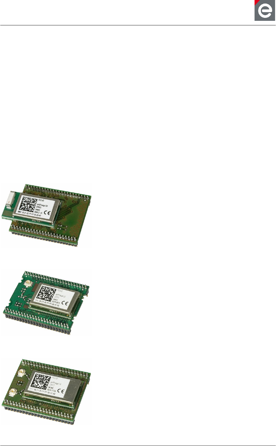
deRFmega128-22M00
deRFmega128-22M10
deRFmega128-22M12
Document Version V1.1c
2013-07-01

User Manual
Version 1.1c
2013-07-01
OEM radio modules deRFmega
www.dresden-elektronik.de
Page 2 of 52
Table of contents
1. Overview ......................................................................................................................... 6
2. Applications ..................................................................................................................... 6
3. Features .......................................................................................................................... 7
3.1. deRFmega128-22M00 ............................................................................................ 7
3.2. deRFmega128-22M10 ............................................................................................ 8
3.3. deRFmega128-22M12 ............................................................................................ 9
4. Technical data ............................................................................................................... 10
4.1. TX Power register settings for deRFmega128-22M00 and 22M10 ........................ 13
4.2. TX Power register settings for deRFmega128-22M12 .......................................... 14
4.3. Output power and duty cycle settings for deRFmega128-22M00 .......................... 15
4.4. Output power and duty cycle settings for deRFmega128-22M12 .......................... 16
5. Mechanical size ............................................................................................................. 17
5.1. deRFmega128-22M00 .......................................................................................... 17
5.2. deRFmega128-22M10 .......................................................................................... 18
5.3. deRFmega128-22M12 .......................................................................................... 19
6. Soldering profile............................................................................................................. 20
7. Pin assignment .............................................................................................................. 21
7.1. Signals of deRFmega128-22M00 ......................................................................... 21
7.2. Signals of deRFmega128-22M10 ......................................................................... 24
7.2.1. External front-end and antenna diversity control ....................................... 27
7.3. Signals of deRFmega128-22M12 ......................................................................... 28
7.3.1. Internal front-end control ........................................................................... 31
7.4. Signal description ................................................................................................. 32
8. PCB design ................................................................................................................... 34
8.1. Technology ........................................................................................................... 34
8.2. Base board footprint ............................................................................................. 34
8.2.1. Footprint of deRFmega128-22M00 ........................................................... 35
8.2.2. Footprint of deRFmega128-22M10 ........................................................... 36
8.2.3. Footprint of deRFmega128-22M12 ........................................................... 37
8.3. Ground plane........................................................................................................ 37
8.4. Layers .................................................................................................................. 38
8.5. Traces .................................................................................................................. 39
8.6. Placement on the PCB ......................................................................................... 40
9. Clock ............................................................................................................................. 41
10. Application circuits ......................................................................................................... 42
10.1. UART ................................................................................................................... 42
10.2. ISP ....................................................................................................................... 42
10.3. JTAG .................................................................................................................... 42
10.4. TWI ...................................................................................................................... 43
10.5. External front-end and antenna diversity .............................................................. 44
11. Programming ................................................................................................................. 46

User Manual
Version 1.1c
2013-07-01
OEM radio modules deRFmega
www.dresden-elektronik.de
Page 3 of 52
12. Pre-flashed firmware ..................................................................................................... 46
13. Adapter boards .............................................................................................................. 46
14. Radio certification .......................................................................................................... 47
14.1. United States (FCC) ............................................................................................. 47
14.2. European Union (ETSI) ........................................................................................ 48
14.3. Approved antennas .............................................................................................. 48
15. Ordering information ...................................................................................................... 49
16. Packaging dimension .................................................................................................... 50
17. Revision notes ............................................................................................................... 50
18. References .................................................................................................................... 51

User Manual
Version 1.1c
2013-07-01
OEM radio modules deRFmega
www.dresden-elektronik.de
Page 4 of 52
Document history
Date
Version
Description
2012-10-15
1.0
Initial version
2012-11-30
1.1
Update technical data
TX_PWR register settings
Sensitivity
Update signal description
2013-02-25
1.1a
RFOUT pin description on deRFmega128-22M12
more precisely specified
Update FCC section
2013-07-01
1.1c
Update Duty Cycle

User Manual
Version 1.1c
2013-07-01
OEM radio modules deRFmega
www.dresden-elektronik.de
Page 5 of 52
Abbreviations
Abbreviation
Description
IEEE 802.15.4
IEEE 802.15.4 standard, applicable to low-rate Wireless Personal Area
Networks (WPAN)
6LoWPAN
IPv6 over Low Power Wireless Personal Area Networks
ADC
Analog to Digital Converter
CE
Consumer Electronics
EMI
Electromagnetic Interference
ETSI
European Telecommunications Standards Institute
FCC
Federal Communications Commission
GPIO
Generals Purpose Input Output
JTAG
Joint Test Action Group, digital interface for debugging of embedded
devices, also known as IEEE 1149.1 standard interface
ISA SP100
International Society of Automation, the Committee establishes standards
and related technical information for implementing wireless systems.
ISP
In-System-Programming
LGA
Land Grid Array, a type of surface-mount packaging for integrated circuits
LNA
Low Noise Amplifier
MAC
Medium (Media) Access Control
MCU, µC
Microcontroller Unit
PA
Power Amplifier
PCB
Printed Circuit Board
PWM
Pulse Width Modulation
RF
Radio Frequency
R&TTE
Radio and Telecommunications Terminal Equipment
(Directive of the European Union)
SPI
Serial Peripheral Interface
TWI
Two-Wire Serial Interface
U[S]ART
Universal [Synchronous/]Asynchronous Receiver Transmitter
USB
Universal Serial Bus
ZigBee
Low-cost, low-power wireless mesh network standard. The ZigBee Alliance
is a group of companies that maintain and publish the ZigBee standard.

User Manual
Version 1.1c
2013-07-01
OEM radio modules deRFmega
www.dresden-elektronik.de
Page 6 of 52
1. Overview
The tiny radio module series by dresden elektronik combines Atmel’s 8-bit AVR single chip
ATmega128RFA1 with a small footprint. Three different module types are available providing
different features for the custom application.
The deRFmega22M00 has an onboard chip antenna to establish a ready-to-use device. No
additional and expensive RF designs are necessary. This module is full compliant to all EU
and US regulatory requirements.
The deRFmega128-22M10 has the smallest form factor of all module types. The customer is
free to design his own antenna, coaxial output or front-end; but it is also possible to use one
of the dresden elektronik’s certified and documented RF designs.
The deRFmega128-22M12 has an onboard front-end feature including LNA and PA with
20 dB gain. Furthermore it supports antenna diversity by a direct connection of two antennas
or coaxial connectors. All necessary RF parts and switches are integrated. This module type
combined with the small form factor is the optimal solution between range extension and
space for mounting on PCB.
2. Applications
The main applications for the radio modules are:
2.4 GHz IEEE 802.15.4
ZigBee PRO
ZigBee RF4CE
ZigBee IP
6LoWPAN
ISA SP100
Wireless Sensor Networks
Industrial and home controlling/monitoring
Smart Metering
User Manual
Version 1.1c
2013-07-01
OEM radio modules deRFmega
www.dresden-elektronik.de
Page 7 of 52
3. Features
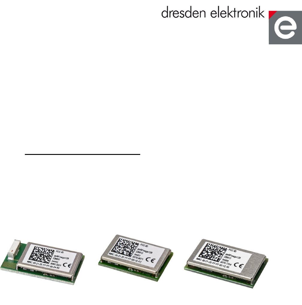
3.1. deRFmega128-22M00
The radio module deRFmega128-22M00 offers the following features:
Tiny size: 23.6 x 13.2 x 3.0 mm
51 LGA pads 0.6 x 0.6 mm
Supply voltage 1.8 V to 3.6 V
RF shielding
Onboard 32.768 kHz crystal
(Deep-Sleep clock) and
16 MHz crystal
Application interfaces:
2x UART, 1x TWI, 1x ADC
GPIO interface
Debug/Programming interfaces:
1x SPI, 1x JTAG, 1x ISP
Onboard 2.4 GHz chip antenna
Certification: CE, FCC
Figure 1 shows the block diagram of the radio module deRFmega128-22M00.
ATmega128RFA1
Transceiver crystal
16MHz [+/-10ppm]
JTAG
UART
VCC
1.8V to 3.6V
Watch crystal
32.768kHz
SPI
TWI
ADC
GPIO
2.4GHz antenna
Figure 1: Block diagram deRFmega128-22M00
User Manual
Version 1.1c
2013-07-01
OEM radio modules deRFmega
www.dresden-elektronik.de
Page 8 of 52
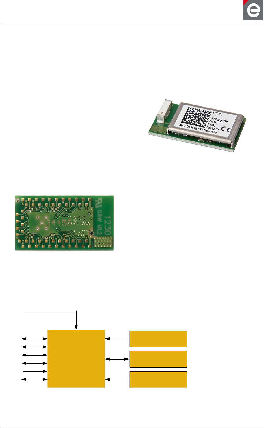
3.2. deRFmega128-22M10
The radio module deRFmega128-22M10 offers the following features:
Tiny size: 19.0 x 13.2 x 3.0 mm
55 LGA pads 0.6 x 0.6 mm
Supply voltage 1.8 V to 3.6 V
RF shielding
Onboard 32.768 kHz crystal
(Deep-Sleep clock) and
16 MHz crystal
Application interfaces:
2x UART, 1x TWI, 1x ADC
GPIO interface
Debug/Programming interfaces:
1x SPI, 1x JTAG, 1x ISP
Solderable 2.4 GHz RF output pads
(1x RFOUT, 3x RFGND)
Certification: CE, FCC pending
Figure 2 shows the block diagram of the radio module deRFmega128-22M10.
ATmega128RFA1
Transceiver crystal
16MHz [+/-10ppm]
JTAG
UART
VCC
1.8V to 3.6V
Watch crystal
32.768kHz
SPI
TWI
ADC
GPIO
RFout
Figure 2: Block diagram deRFmega128-22M10
User Manual
Version 1.1c
2013-07-01
OEM radio modules deRFmega
www.dresden-elektronik.de
Page 9 of 52
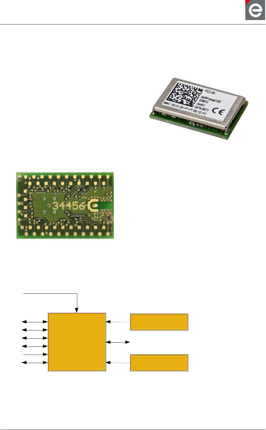
3.3. deRFmega128-22M12
The radio module deRFmega128-22M12 offers the following features:
Tiny size: 21.5 x 13.2 x 3.0 mm
59 LGA pads 0.6 x 0.6 mm
Supply voltage 2.0 V to 3.6 V
Antenna diversity support
RF shielding
Onboard 32.768 kHz crystal
(Deep-Sleep clock) and
16 MHz crystal
Application interfaces:
2x UART, 1x TWI
GPIO interface
Debug/Programming interfaces:
1x SPI, 1x JTAG, 1x ISP
2.4 GHz front-end module with
internal 20 dB PA and LNA
Solderable 2.4 GHz RF output pad
(2x RFOUT, 6x RFGND)
Certification: CE, FCC pending
Figure 3 shows the block diagram of the radio module deRFmega128-22M12.
ATmega128RFA1
Transceiver crystal
16MHz [+/-10ppm]
JTAG
UART
VCC
2.0V to 3.6V
Watch crystal
32.768kHz
SPI
TWI
ADC
GPIO
2.4GHz Front-End RFout 1
RFout 2
RF
Control
Figure 3: Block diagram deRFmega128-22M12
User Manual
Version 1.1c
2013-07-01
OEM radio modules deRFmega
www.dresden-elektronik.de
Page 10 of 52
4. Technical data
Table 4-1: Mechanical data
Mechanical
Radio modules
Size (L x W x H)
23.6 x 13.2 x 3.0 mm (for 22M00)
19.0 x 13.2 x 3.0 mm (for 22M10)
21.5 x 13.2 x 3.0 mm (for 22M12)
Pads
Type
LGA
Pitch
1.60 mm
Pad size
0.6 x 0.6 mm
Table 4-2: Temperature range
Temperature range
Parameter
Min
Typ
Max
Unit
Operating
temperature range
Twork
-40
+85
°C
Humidity
25
80
% r.H.
Storage
temperature range
Tstorage
-40
+125
°C
Table 4-3: Electrical data
Electrical
deRFmega128-22M00 and deRFmega128-22M10
Parameter
Min
Typ
Max
Unit
Supply Voltage
VCC
1.8
3.3
3.6
V
Current
consumption
ITXon (TX_PWR = +3 dBm)
17.8
18.1
18.2
mA
ITXon (TX_PWR = 0 dBm)
16.2
16.4
16.5
mA
ITXon (TX_PWR = -17 dBm)
12.5
12.7
12.7
mA
IRXon
17.5
17.6
17.7
mA
IIdle (Txoff, MCK = 8MHz)
4.7
4.8
4.8
mA
ISleep
(depends on Sleep Mode)
<1
µA
deRFmega128-22M12
Parameter
Min
Typ
Max
Unit
Supply Voltage
VCC
2.0
3.3
3.6
V
User Manual
Version 1.1c
2013-07-01
OEM radio modules deRFmega
www.dresden-elektronik.de
Page 11 of 52
Current
consumption
ITXon (TX_PWR = +20 dBm)
119.4
197.7
205.2
mA
ITXon (TX_PWR = +4 dBm)
27.0
46.1
46.7
mA
IRXon
19.8
22.5
22.8
mA
IIdle (Txoff, MCK = 8 MHz)
5.2
5.4
5.6
mA
ISleep
(depends on Sleep Mode)
<1
µA
Table 4-4: Quartz crystal properties
Quartz crystal
Parameter
Min
Typ
Max
Unit
Watch crystal
Frequency
32.768
kHz
Frequency tolerance
+/-20
ppm
Transceiver crystal
Frequency
16.000
MHz
Frequency tolerance
+/-10
ppm
Table 4-5: Radio data of deRFmega128-22M00 and deRFmega128-22M10
Radio 2.4 GHz (Supply voltage VCC = 3.3V)
Parameter / feature
Min
Typ
Max
Unit
Antenna
Type
Chip ceramic
Gain
-0.7
dBi
Diversity
No
RF Pad
Impedance
50
Ω
Range
Line of sight
TBD
m
Frequency range1
PHY_CC_CCA = 0x0B...0x1A
2405
2480
MHz
Channels
PHY_CC_CCA = 0x0B...0x1A
16
Transmitting
power conducted
TX_PWR = 0x00
VCC = 3.3V
2.3
2.9
dBm
Receiver sensitivity
Data Rate = 250 kBit/s
Data Rate = 500 kBit/s
Data Rate = 1000 kBit/s
Data Rate = 2000 kBit/s
-98
-94
-91
>-80
dBm
dBm
dBm
dBm
1
Operating the transmitter at channel 11 to 25 requires a duty cycle ≤35% and channel 26 requires a
duty cycle ≤15% to fulfil all requirements according to FCC Part 15 Subpart C § 15.209. See chapter
4.3 for further information.
User Manual
Version 1.1c
2013-07-01
OEM radio modules deRFmega
www.dresden-elektronik.de
Page 12 of 52
Data rate (gross)
TRX_CTRL_2 = 0x00
TRX_CTRL_2 = 0x01
TRX_CTRL_2 = 0x02
TRX_CTRL_2 = 0x03
250
500
1000
2000
kBit/s
kBit/s
kBit/s
kBit/s
EVM
conducted
6.5
7.5
10.5
%
Table 4-6: Radio data of deRFmega128-22M12
Radio (Supply voltage VCC = 3.3V)
Parameter / feature
Min
Typ
Max
Unit
RF pad
Impedance
50
Ω
Diversity
Yes
Range
TBD
m
Frequency range
2405
2480
MHz
Channels
16
Transmitting
power conducted2,3
TX_PWR = 0x00
VCC = 3.3V
21.4
21.9
22.4
dBm
Receiver sensitivity
Data Rate = 250 kBit/s
Data Rate = 500 kBit/s
Data Rate = 1000 kBit/s
Data Rate = 2000 kBit/s
-105
-100
-98
-91
dBm
dBm
dBm
dBm
Data rate (gross)
TRX_CTRL_2 = 0x00
TRX_CTRL_2 = 0x01
TRX_CTRL_2 = 0x02
TRX_CTRL_2 = 0x03
250
500
1000
2000
kBit/s
kBit/s
kBit/s
kBit/s
EVM
conducted
6.5
7.5
9.5
%
2
Only applicable for EU: The maximum allowed TX_PWR register setting of deRFmega128-22M12 is
TX_PWR = 0x0E. According to EN 300 328 clause 4.3.1 the maximum transmit power is restricted to
a limit of +10dBm.
3
Only applicable for US: Operating the transmitter at channel 11, 12, 13, 23, 24, 25 and 26 requires to
ensure a reduced output power and/or duty cycle limit to fulfil all requirements according to FCC Part
15 Subpart C § 15.209. See chapter 4.3.
User Manual
Version 1.1c
2013-07-01
OEM radio modules deRFmega
www.dresden-elektronik.de
Page 13 of 52
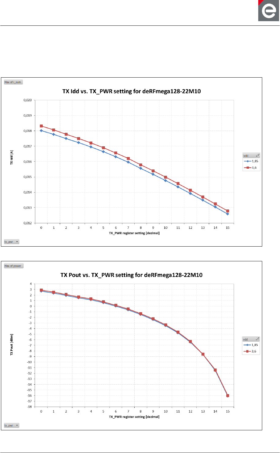
4.1. TX Power register settings for deRFmega128-22M00 and 22M10
The diagrams in Figure 4 and Figure 5 are showing the current consumption and conducted
output power during transmission depending on the TX_PWR register setting. The values are
valid for deRFmega128-22M00 and 22M10.
Figure 4: TX Idd vs. TX_PWR for deRFmega128-22M00 / 22M10
Figure 5: TX Pout vs. TX_PWR for deRFmega128-22M00 / 22M10
User Manual
Version 1.1c
2013-07-01
OEM radio modules deRFmega
www.dresden-elektronik.de
Page 14 of 52
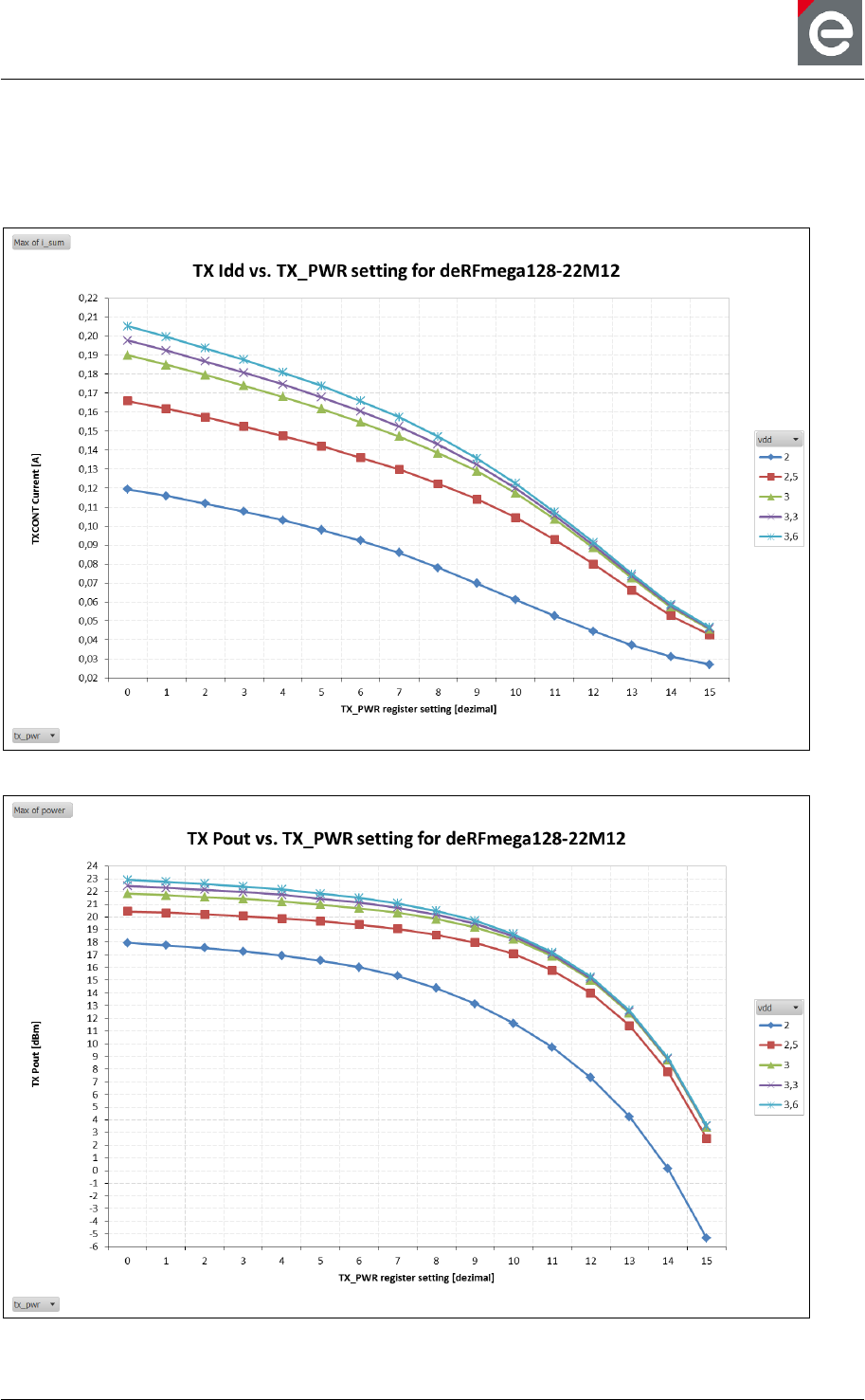
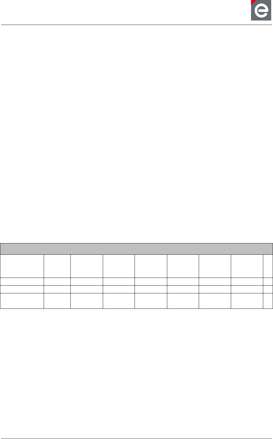
4.2. TX Power register settings for deRFmega128-22M12
The diagrams in Figure 6 and Figure 7 showing the current consumption and conducted
output power during transmission depending on the TX_PWR register setting. The values are
valid for deRFmega128-22M12.
Figure 6: TX Idd vs. TX_PWR for deRFmega128-22M12
Figure 7: TX Pout vs. TX_PWR for deRFmega128-22M12
User Manual
Version 1.1c
2013-07-01
OEM radio modules deRFmega
www.dresden-elektronik.de
Page 15 of 52
4.3. Output power and duty cycle settings for deRFmega128-22M00
The radio module deRFmega128-22M00 must observe the duty cycle settings to be
compliant with all FCC regulatory requirements.
The requirements are a duty cycle which is ≤15% for channel 26 operation and ≤36% for the
remaining channels. The duty cycle is related to a period of 100ms, where the given value
defines the TX-ON time. That means, the maximum allowed TX-ON time is 15ms within a
period of 100ms for channel 26 and 36ms for all other channels respectively.
The available default firmware for the radio modules is a ‘Wireless UART’ (WUART) that
transmits wireless data inputs from one node to another. The WUART packets length
including overhead ranges between of 12 and 127 bytes. All radio protective systems like
automated acknowledgement, CSMA-CA and frame-retry are activated. Therefore sending a
packet with maximum length takes approximately 4ms to from start to end of transmission.
Before each transmission, a fixed delay time of 30ms is defined, to ensure that the available
maximum packet length is used. This optimizes the energy performance of the radio module,
because not every single data input will be transmitted separately. The fixed delay time
cannot be changed by software. By default, the WUART firmware operates at channel 20
which also cannot be changed by the user.
Table 4-7 shows a worst case scenario of data transmission with maximum packet length of
127 bytes. The data input will be buffered within the 30ms delay and then transmitted. The
CSMA-CA wait time is assumed to be zero. Here, the RX-ON time of receiving the
automated acknowledgement after each transmission is ignored. The transition will be
continued until all data inputs are successfully transmitted. Therefore, the resulting duty cycle
is ≤ 12% and fulfills the FCC requirements for all channels.
Table 4-7: Timeline
Data transmission timeline
Operation
State
buffer
input
data
transmit
data
buffer
input
data
transmit
data
buffer
input
data
transmit
data
buffer
input
data
TX State
OFF
ON
OFF
ON
OFF
ON
OFF
…
Duration [ms]
30
4
30
4
30
4
30
…
Time [ms]
0..
30
30..
34
34..
64
64..
68
68..
98
98..
102
102..
132
…
User Manual
Version 1.1c
2013-07-01
OEM radio modules deRFmega
www.dresden-elektronik.de
Page 16 of 52
4.4. Output power and duty cycle settings for deRFmega128-22M12
The radio module deRFmega128-22M12 is able to provide an output power greater than
20dBm. Table 4-8 defines the necessary power settings of the TX_PWR register [1], which
must be set to fulfill all national requirements of Europe (EN 300 328) and USA (CFR 47
Ch. I FCC Part 15). The duty cycle defines the relationship between the radio-on time and
the period of 100ms.
Channel
ETSI
FCC
TX_PWR
[hex]
Duty Cycle
[%]
TX_PWR
[hex]
Duty Cycle
[%]
11
0x0E
100
0x0B
100
12
0x0E
100
0x02
100
13
0x0E
100
0x01
100
14
0x0E
100
0x00
100
15
0x0E
100
0x00
100
16
0x0E
100
0x00
100
17
0x0E
100
0x00
100
18
0x0E
100
0x00
100
19
0x0E
100
0x00
100
20
0x0E
100
0x00
100
21
0x0E
100
0x00
100
22
0x0E
100
0x00
100
23
0x0E
100
0x06
100
24
0x0E
100
0x0D
100
25
0x0E
100
0x0F
100
26
0x0E
100
0x0F
30
Table 4-8: power table for deRFmega128-22M12
User Manual
Version 1.1c
2013-07-01
OEM radio modules deRFmega
www.dresden-elektronik.de
Page 17 of 52
5. Mechanical size
The following section show the mechanical dimensions of the different radio modules. All
distances are given in millimeters.
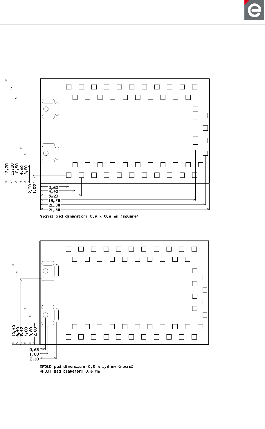
5.1. deRFmega128-22M00
The module has a size of 23.6 x 13.2 mm and a height of 3.0 mm. The LGA pads are
arranged in a double row design. Figure 8 shows the details from top view.
Figure 8: Module dimension and signal pads geometry deRFmega128-22M00 (top view)
User Manual
Version 1.1c
2013-07-01
OEM radio modules deRFmega
www.dresden-elektronik.de
Page 18 of 52
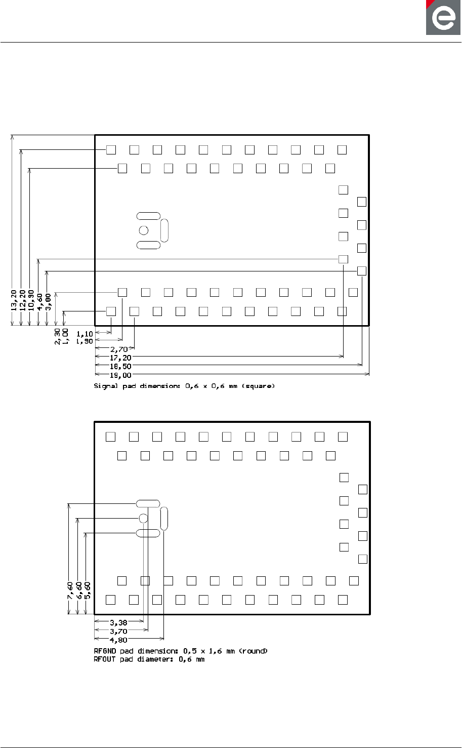
5.2. deRFmega128-22M10
The module has a size of 19.0 x 13.2 mm and a height of 3.0 mm. The LGA pads are
arranged in a double row design. The RF pads consist of three ground pads and one signal
pad. Figure 9 and Figure 10 shows the details from top view.
Figure 9: Module dimension and signal pad geometry deRFmega128-22M10 (top view)
Figure 10: RF pad geometry deRFmega128-22M10 (top view)
User Manual
Version 1.1c
2013-07-01
OEM radio modules deRFmega
www.dresden-elektronik.de
Page 19 of 52
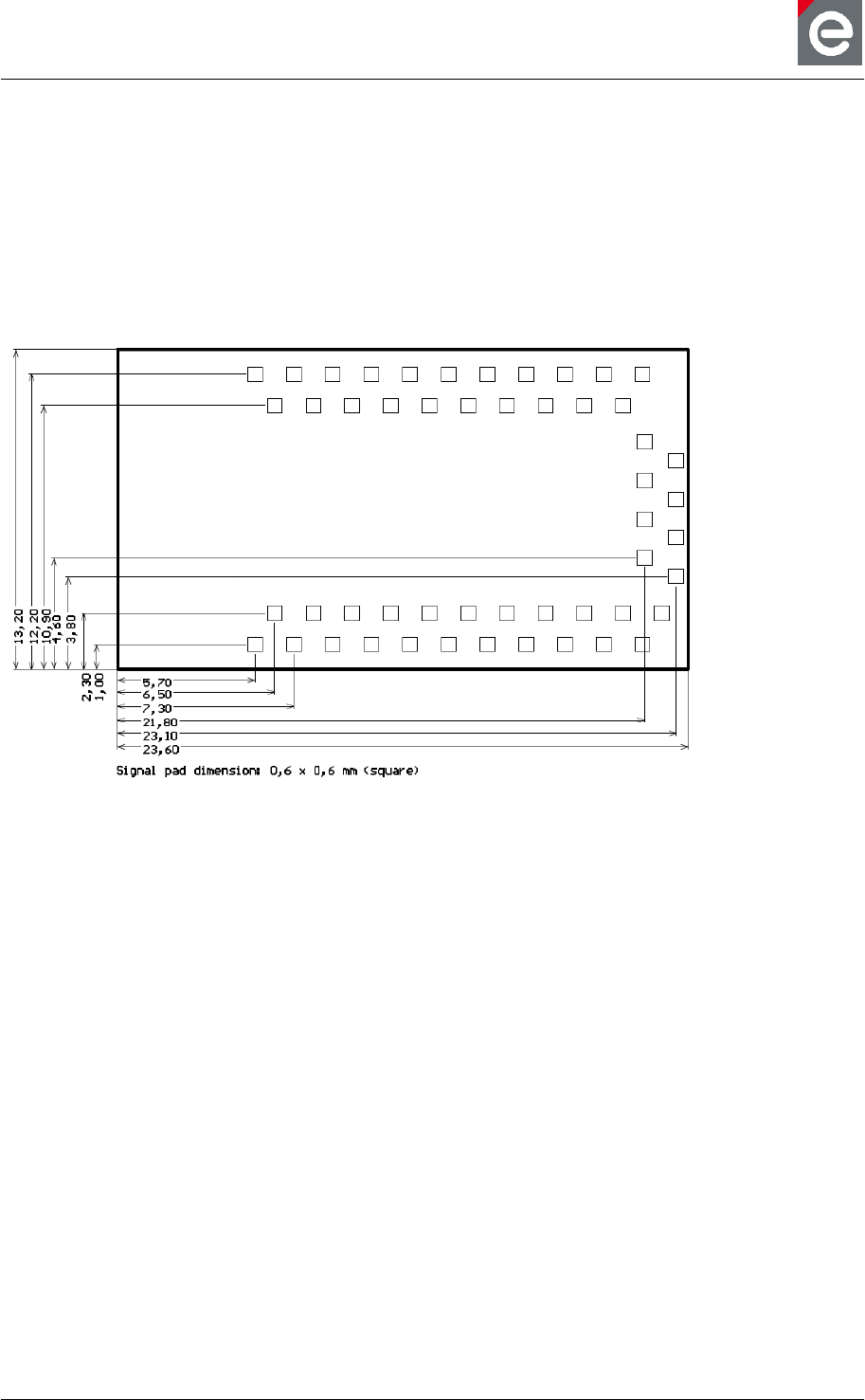
5.3. deRFmega128-22M12
The module has a size of 21.5 x 13.2 mm and a height of 3.0 mm. The LGA pads are
designed in a zigzag structure. The RF pads consist of six ground pads and two signal pads.
Figure 11 and Figure 12 show the details from top view.
Figure 11: Module dimension and signal pad geometry deRFmega128-22M12 (top view)
Figure 12: RF pad geometry deRFmega128-22M12 (top view)
User Manual
Version 1.1c
2013-07-01
OEM radio modules deRFmega
www.dresden-elektronik.de
Page 20 of 52
6. Soldering profile
Table 6-1 shows the recommended soldering profile for the radio modules.
Table 6-1: Soldering Profile
Profile Feature
Values
Average-Ramp-up Rate (217°C to Peak)
3°C/s max
Preheat Temperature 175°C ±25°C
180 s max
Temperature Maintained Above 217°C
60 s to 150 s
Time within 5°C of Actual Peak Temperature
20 s to 40 s
Peak Temperature Range
260°C
Ramp-down Rate
6°C/s max
Time 25°C to Peak Temperature
8 min max
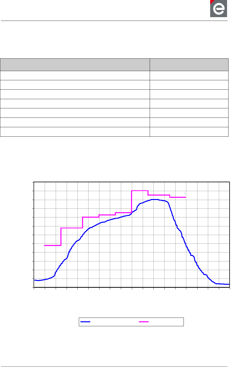
Figure 13 shows a recorded soldering profile for a radio module. The blue colored line
illustrates a temperature sensor placed next to the soldering contacts of the radio module.
The pink line shows the set temperatures depending on the zone within the reflow soldering
machine.
40
60
80
100
120
140
160
180
200
220
240
260
280
0
20
40
60
80
100
120
140
160
180
200
220
240
260
280
300
320
340
360
t [s]
T [°C]
Measured Temp. Zone Temp.
Figure 13: Recorded soldering profile
A solder process without supply of nitrogen causes a discoloration of the metal RF-shielding.
User Manual
Version 1.1c
2013-07-01
OEM radio modules deRFmega
www.dresden-elektronik.de
Page 21 of 52
7. Pin assignment
The LGA pads provide all signals to the customer: power supply, peripheral, programming,
debugging, tracing, analog measurement, external front-end control, antenna diversity
control and free programmable ports. All provided signals except VCC, DGND, RSTN,
RSTON, AREF, AVDD and CLKI are free programmable port pins (GPIO).
7.1. Signals of deRFmega128-22M00
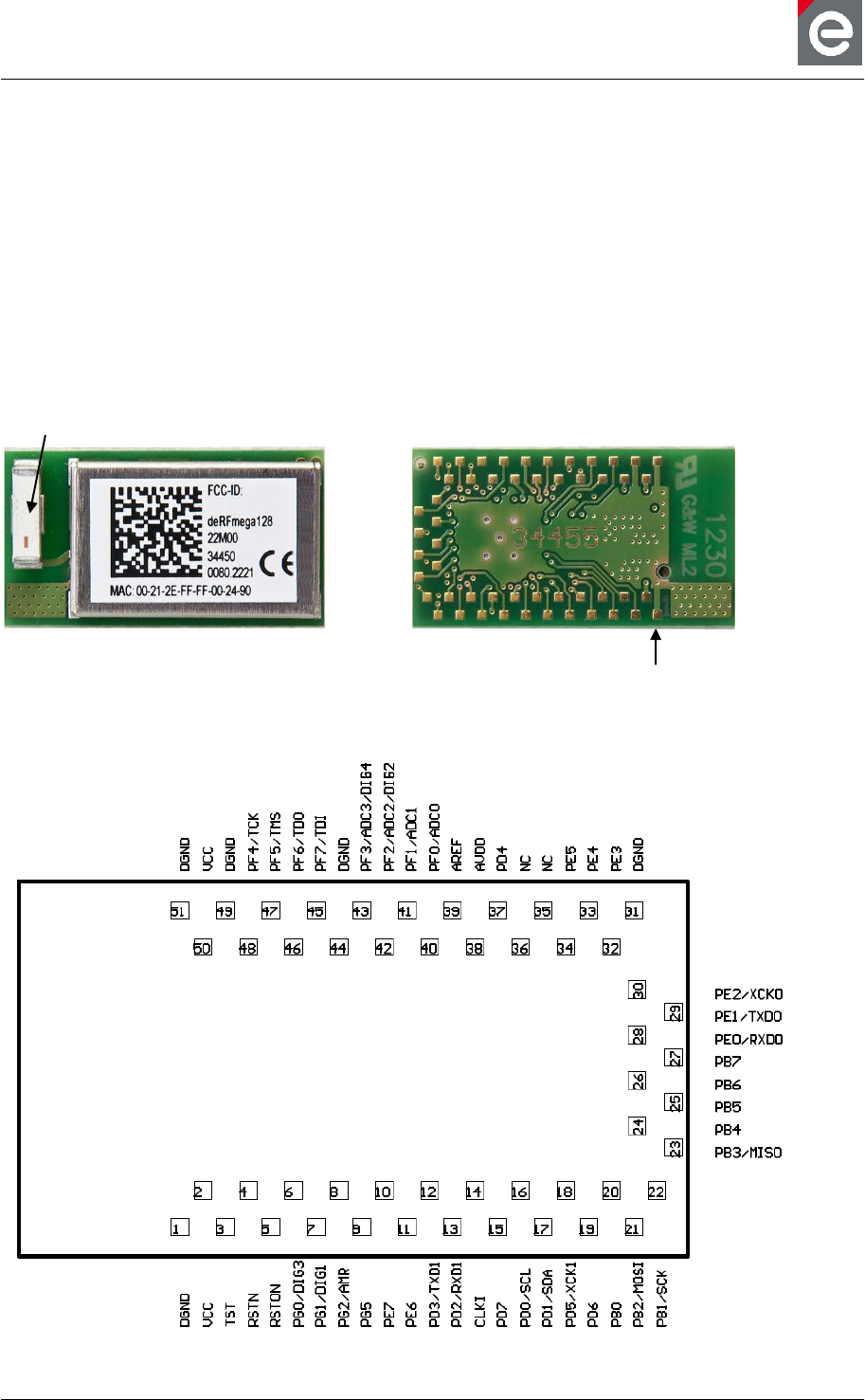
The radio module deRFmega128-22M00 has 51 LGA pads. The ‘1’ marking is shown in
Figure 15. Consider that the pin numbering in Figure 16 is shown from top view. All
available LGA pads are listed in Table 7-1.
Figure 14: deRFmega128-22M00 (top view)
Figure 15: deRFmega128-22M00 (bottom view)
Figure 16: Pad numbering and signal names of deRFmega128-22M00 (top view)
pad 1
Antenna

User Manual
Version 1.1c
2013-07-01
OEM radio modules deRFmega
www.dresden-elektronik.de
Page 22 of 52
Table 7-1: I/O port pin to LGA pad mapping for deRFmega128-22M10
I/O port pin mapping
LGA
Pad
MCU
Pin
Primary
function
Alternate functions
Comments
GND
2
-
VCC
1.8 V to 3.6 V
3
11
TST
Must be connected to GND!
4
12
RSTN
Reset
5
13
RSTON
Reset output
6
14
PG0
DIG3
7
15
PG1
DIG1
8
16
PG2
AMR
9
19
PG5
OC0B
10
53
PE7
ICP3
INT7
CLKO
11
52
PE6
T3
INT6
Timer3
12
28
PD3
TXD1
INT3
UART1
13
27
PD2
RXD1
INT2
UART1
14
33
CLKI
External clock input
15
32
PD7
T0
16
25
PD0
SCL
INT0
TWI
17
26
PD1
SDA
INT1
TWI
18
30
PD5
XCK1
19
31
PD6
T1
Timer1
20
36
PB0
SS
PCINT0
SPI
21
38
PB2
MOSI
PDI
PCINT2
SPI, ISP
22
37
PB1
SCK
PCINT1
SPI
23
39
PB3
MISO
PDO
PCINT3
SPI, ISP
24
40
PB4
OC2A
PCINT4
25
41
PB5
OC1A
PCINT5
26
42
PB6
OC1B
PCINT6
27
43
PB7
OC0A
OC1C
PCINT7
28
46
PE0
RXD0
PCINT8
UART0
29
47
PE1
TXD0
UART0
30
48
PE2
XCK0
AIN0
UART0
31
-
GND
User Manual
Version 1.1c
2013-07-01
OEM radio modules deRFmega
www.dresden-elektronik.de
Page 23 of 52
32
49
PE3
OC3A
AIN1
33
5
PE4
OC3B
INT4
34
51
PE5
OC3C
INT5
35
-
NC
Leave unconnected
36
-
NC
Leave unconnected
37
29
PD4
ICP1
38
60
AVDD
Leave unconnected if unused
(1.8V TRX Voltage Output)
39
62
AREF
40
63
PF0
ADC0
ADC
41
64
PF1
ADC1
ADC
42
1
PF2
ADC2
DIG2
ADC
43
2
PF3
ADC3
DIG4
44
-
GND
45
6
PF7
ADC7
TDI
JTAG
46
5
PF6
ADC6
TDO
JTAG
47
4
PF5
ADC5
TMS
JTAG
48
3
PF4
ADC4
TCK
JTAG
49
-
GND
50
-
VCC
1.8 V to 3.6 V
51
-
GND
Note: PG4/TOSC1 and PG3/TOSC2 are connected to a 32.768 kHz crystal internally.
User Manual
Version 1.1c
2013-07-01
OEM radio modules deRFmega
www.dresden-elektronik.de
Page 24 of 52
7.2. Signals of deRFmega128-22M10
The radio module deRFmega128-22M10 has 55 LGA pads. The ‘1’ marking is shown in
Figure 18. Consider that the pin numbering in Figure 19 is shown from top view. All LGA
pads are listed in Table 7-2.
Figure 17: deRFmega128-22M10 (top view)
Figure 18: deRFmega128-22M10 (bottom view)
Figure 19: Pad numbering and signal names of deRFmega128-22M10 (top view)
pad 1
RFOUT

User Manual
Version 1.1c
2013-07-01
OEM radio modules deRFmega
www.dresden-elektronik.de
Page 25 of 52
Table 7-2: I/O port pin to LGA pad mapping for deRFmega128-22M10
I/O port pin mapping
LGA
Pad
MCU
Pin
Primary
function
Alternate functions
Comments
1
-
GND
2
-
VCC
1.8 V to 3.6 V
3
11
TST
Must be connected to GND!
4
12
RSTN
Reset
5
13
RSTON
Reset output
6
14
PG0
DIG3
External Front-End control
7
15
PG1
DIG1
External diversity control
8
16
PG2
AMR
9
19
PG5
OC0B
10
53
PE7
ICP3
INT7
CLKO
11
52
PE6
T3
INT6
Timer3
12
28
PD3
TXD1
INT3
UART1
13
27
PD2
RXD1
INT2
UART1
14
33
CLKI
External clock input
15
32
PD7
T0
16
25
PD0
SCL
INT0
TWI
17
26
PD1
SDA
INT1
TWI
18
30
PD5
XCK1
19
31
PD6
T1
Timer1
20
36
PB0
SS
PCINT0
SPI
21
38
PB2
MOSI
PDI
PCINT2
SPI, ISP
22
37
PB1
SCK
PCINT1
SPI
23
39
PB3
MISO
PDO
PCINT3
SPI, ISP
24
40
PB4
OC2A
PCINT4
25
41
PB5
OC1A
PCINT5
26
42
PB6
OC1B
PCINT6
27
43
PB7
OC0A
OC1C
PCINT7
28
46
PE0
RXD0
PCINT8
UART0
29
47
PE1
TXD0
UART0
30
48
PE2
XCK0
AIN0
UART0
31
-
GND
User Manual
Version 1.1c
2013-07-01
OEM radio modules deRFmega
www.dresden-elektronik.de
Page 26 of 52
32
49
PE3
OC3A
AIN1
33
5
PE4
OC3B
INT4
34
51
PE5
OC3C
INT5
35
-
NC
Leave unconnected
36
-
NC
Leave unconnected
37
29
PD4
ICP1
38
60
AVDD
Leave unconnected if unused
(1.8V TRX Voltage Output)
39
62
AREF
40
63
PF0
ADC0
ADC
41
64
PF1
ADC1
ADC
42
1
PF2
ADC2
DIG2
ADC
43
2
PF3
ADC3
DIG4
External Front-End control
44
-
GND
45
6
PF7
ADC7
TDI
JTAG
46
5
PF6
ADC6
TDO
JTAG
47
4
PF5
ADC5
TMS
JTAG
48
3
PF4
ADC4
TCK
JTAG
49
-
GND
50
-
VCC
1.8 V to 3.6 V
51
-
GND
52
-
RFGND
53
-
RFOUT
50 Ω impedance
54
-
RFGND
55
-
RFGND
Note: PG4/TOSC1 and PG3/TOSC2 are internally connected to a 32.768 kHz crystal.
User Manual
Version 1.1c
2013-07-01
OEM radio modules deRFmega
www.dresden-elektronik.de
Page 27 of 52
7.2.1. External front-end and antenna diversity control
The radio module deRFmega128-22M10 offers the possibility to control external front-end
components and to support antenna diversity. Table 7-3 and Table 7-4 show the logic values
of the control signals. A logic ‘0’ is specified with a voltage level of 0 V to 0.3 V. A logic ‘1’ is
specified with a value of VCC - 0.3 V to 3.6 V.
An application circuit is shown in Section 10.5.
Antenna Diversity
The antenna diversity algorithm is enabled with setting bit ANT_DIV_EN=1 in the ANT_DIV
register. The external control of RF switches must be enabled by bit ANT_EXT_SW_EN of
the same register. This action will configure the pins DIG1 and DIG2 as outputs. Both pins
are used to feed the RF switch signal and its inverse to the differential inputs of the RF
switch. Please refer to ATmega128RFA1 datasheet [1] to get information to all register
settings.
Table 7-3: Antenna diversity control
Mode description
PG1/DIG1
PF2/DIG2
TRX off
Sleep mode
Disable register bit ANT_EXT_SW_EN and set port
pins DIG1 and DIG2 to output low via I/O port control
registers. This action could reduce the power
consumption of an external RF switch.
ANT0
1
0
ANT1
0
1
Front-End
The control of front-end components can be realized with the signals DIG3 and DIG4. The
function will be enabled with bit PA_EXT_EN of register TRX_CTRL_1 which configures both
pins as outputs. While transmission is turned off DIG3 is set to ‘0’ and DIG4 is set to ‘1’.
When the transceiver starts transmission the polarity will be changed. Both pins can be used
to control PA, LNA and RF switches. Please refer to ATmega128RFA1 datasheet [1] to get
information to all register settings.
Table 7-4: Front-end control
PG0/DIG3
PF3/DIG4
TRX off
Sleep mode
Disable register bit PA_EXT_EN and set port pins
DIG3 and DIG4 to output low via I/O port control
registers. This action may reduce the power
consumption of external front-end devices.
TRX off
0
1
TRX on
1
0
Sleep mode
To optimize the power consumption of external front-end components, it is possible to use a
dedicated GPIO to set the PA into sleep mode, if applicable or to switch an additionally
MOSFET, which supplies the PA.
User Manual
Version 1.1c
2013-07-01
OEM radio modules deRFmega
www.dresden-elektronik.de
Page 28 of 52
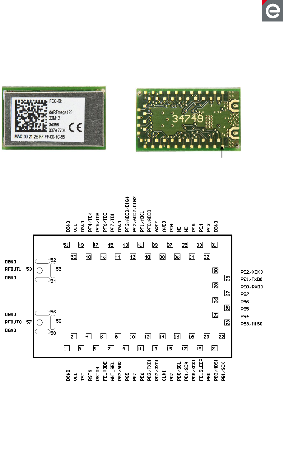
7.3. Signals of deRFmega128-22M12
The radio module deRFmega128-22M10 has 59 LGA pads. The ‘1’ marking is shown in
Figure 21. Consider that the pin numbering in Figure 22 is shown from top view. All LGA
pads are listed in Table 7-5.
Figure 20: deRFmega128-22M12 (top view)
Figure 21: deRFmega128-22M12 (bottom view)
Figure 22: Pad numbering and signal names of deRFmega128-22M12 (top view)
pad 1
RFOUT1
0
RFOUT2
User Manual
Version 1.1c
2013-07-01
OEM radio modules deRFmega
www.dresden-elektronik.de
Page 29 of 52
Table 7-5: I/O port pin to LGA pad mapping for deRFmega128-22M12
I/O port pin mapping
LGA
Pad
MCU
Pin
Primary
function
Alternate functions
Comments
1
-
GND
2
-
VCC
2.0 V to 3.6 V
3
11
TST
Must be connected to GND!
4
12
RSTN
Reset
5
13
RSTON
Reset output
6
14
PG0
DIG3
Internal connected to PA-CTX4
7
15
PG1
DIG1
Internal connected to PA-ANTSEL4
8
16
PG2
AMR
9
19
PG5
OC0B
10
53
PE7
ICP3
INT7
CLKO
11
52
PE6
T3
INT6
Timer3
12
28
PD3
TXD1
INT3
UART1
13
27
PD2
RXD1
INT2
UART1
14
33
CLKI
External clock input
15
32
PD7
T0
16
25
PD0
SCL
INT0
TWI
17
26
PD1
SDA
INT1
TWI
18
30
PD5
XCK1
19
31
PD6
T1
Internal connected to PA-CSD4
20
36
PB0
SS
PCINT0
SPI
21
38
PB2
MOSI
PDI
PCINT2
SPI, ISP
22
37
PB1
SCK
PCINT1
SPI
23
39
PB3
MISO
PDO
PCINT3
SPI, ISP
24
40
PB4
OC2A
PCINT4
25
41
PB5
OC1A
PCINT5
26
42
PB6
OC1B
PCINT6
27
43
PB7
OC0A
OC1C
PCINT7
28
46
PE0
RXD0
PCINT8
UART0
29
47
PE1
TXD0
UART0
30
48
PE2
XCK0
AIN0
UART0
4
See Section 7.3.1
User Manual
Version 1.1c
2013-07-01
OEM radio modules deRFmega
www.dresden-elektronik.de
Page 30 of 52
31
-
GND
32
49
PE3
OC3A
AIN1
33
5
PE4
OC3B
INT4
34
51
PE5
OC3C
INT5
35
-
NC
Leave unconnected
36
-
NC
Leave unconnected
37
29
PD4
ICP1
38
60
AVDD
Leave unconnected if unused
(1.8V TRX Voltage Output)
39
62
AREF
40
63
PF0
ADC0
ADC
41
64
PF1
ADC1
ADC
42
1
PF2
ADC2
DIG2
ADC
43
2
PF3
ADC3
DIG4
44
-
GND
45
6
PF7
ADC7
TDI
JTAG
46
5
PF6
ADC6
TDO
JTAG
47
4
PF5
ADC5
TMS
JTAG
48
3
PF4
ADC4
TCK
JTAG
49
-
GND
50
-
VCC
2.0 V to 3.6 V
51
-
GND
52
-
RFGND
53
-
RFOUT2
50 Ω impedance*
54
-
RFGND
55
-
RFGND
56
-
RFGND
57
-
RFOUT1
50 Ω impedance*
58
-
RFGND
59
-
RFGND
Note: PG4/TOSC1 and PG3/TOSC2 are internally connected to a 32.768 kHz crystal.
*) If one of both RFOUT pads of the radio module deRFmega128-22M12 is unused, it
must be terminated with 50 ohms to ground. This action ensures the proper function
of the internal power amplifier and will reduce the power consumption.
User Manual
Version 1.1c
2013-07-01
OEM radio modules deRFmega
www.dresden-elektronik.de
Page 31 of 52
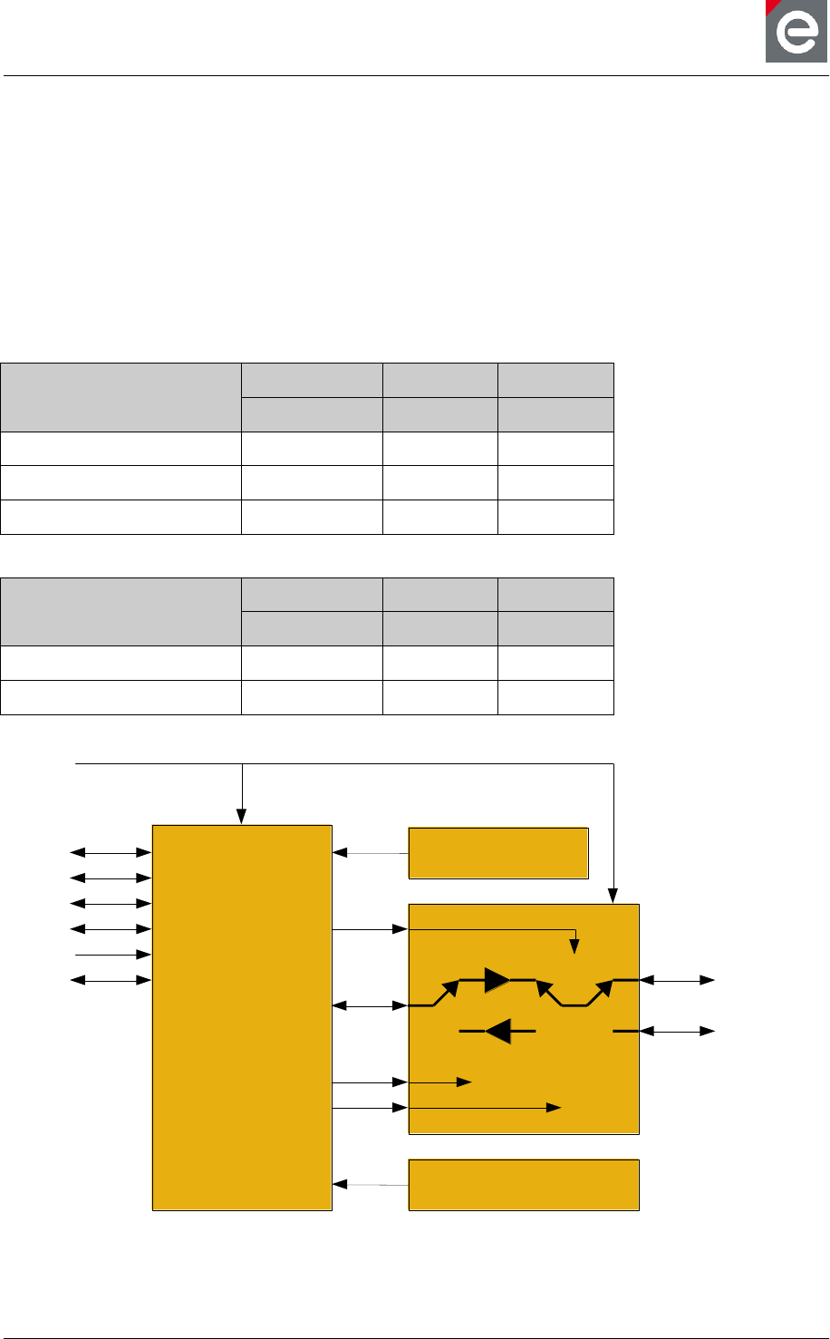
7.3.1. Internal front-end control
The front-end of deRFmega128-22M12 has an internal PA for transmit and a LNA for receive
mode. An additionally antenna diversity feature is usable to select the antenna with the best
link budget. The front-end control includes three MCU port pins (Figure 23). They are used
to choose the TX/RX antenna, de-/activate transmit and receive mode and de-/activate the
sleep mode. Table 7-6 and Table 7-7 show the logic values. A logic ‘0’ is specified with a
voltage level of 0 V to 0.3 V. A logic ‘1’ is specified with a value of VCC - 0.3 V to 3.6 V. The
control signals DIG1, DIG3 and PD6 are available on the LGA pins.
Table 7-6: Front-end control of TX/RX and sleep mode
Mode description
PG1/DIG1
PD6/T1
PG0/DIG3
PA_ANT SEL
PA_CSD
PA_CTX
All off (sleep mode)
X
0
0
RX LNA mode
X
1
0
TX mode
X
1
1
Table 7-7: Front-end control of TX/RX antenna
Mode description
PG1/DIG1
PD6/T1
PG0/DIG3
PA_ANT SEL
PA_CSD
PA_CTX
RFOUT1 port enabled
0
X
X
RFOUT2 port enabled
1
X
X
ATmega128RFA1
Transceiver crystal
16MHz [+/-10ppm]
JTAG
UART
VCC
2.0V to 3.6V
Watch crystal
32.768kHz
SPI
TWI
ADC
GPIO RFout 1
RFout 2
RF
DIG1
PD6
DIG3
ANT SEL
PA
LNA
TX/RX
Sleep
Figure 23: Block diagram of front-end functionality and control
Note: Do not leave any unused RFOUT pad unterminated.
User Manual
Version 1.1c
2013-07-01
OEM radio modules deRFmega
www.dresden-elektronik.de
Page 32 of 52
7.4. Signal description
The available signals are described in Table 7-8. Please refer to ATmega128RFA1
datasheet [1] for more information of all dedicated signals.
Table 7-8: Signal description list
Signal name
Function
Type
Active
Level
Comments
Power
VCC
Voltage Regulator Power Supply
Input
Power
GND
Ground
Clocks and Oscillators
CLKI
External Clock Input
Input
CLKO
Divided System Clock Output
Output
JTAG
TCK
Test Clock
Input
No pull-up resistor
on module
TDI
Test Data In
Input
No pull-up resistor
on module
TDO
Test Data Out
Output
TDM
Test Mode Select
Input
No pull-up resistor
on module
Serial Programming
PDI
Data Input
Input
PDO
Data Output
Output
SCK
Serial Clock
Input
Reset
RSTN
Microcontroller Reset
I/O
Low
Pull-Up resistor5
USART
TXD0 – TXD1
Transmit Data
RXD0 – RXD1
Receive Data
XCK0 – XCK1
Serial Clock
Timer/Counter and PWM Controller
OC0A-OC3A
Output Compare and PWM Output
A for Timer/Counter 0 to 3
OC0B-OC3B
Output Compare and PWM Output
B for Timer/Counter 0 to 3
5
Internal MCU Pull-up resistor
User Manual
Version 1.1c
2013-07-01
OEM radio modules deRFmega
www.dresden-elektronik.de
Page 33 of 52
OC0C-OC3C
Output Compare and PWM Output
C for Timer/Counter 0 to 3
T0, T1, T3
Timer/Counter 0,1,3 Clock Input
Input
ICP1
ICP3
Timer/Counter Input Capture
Trigger 1 and 3
Input
Interrupt
PCINT0 -
PCINT7
Pin Change Interrupt Source 0 to 7
Output
INT0 – INT7
External Interrupt Input 0 to7
Input
SPI
MISO
SPI Master In/Slave Out
I/O
MOSI
SPI Master Out/Slave In
I/O
SCK
SPI Bus Serial Clock
I/O
SSN
SPI Slave Port Select
I/O
Two-Wire-Interface
SDA
Two-Wire Serial Interface Data
I/O
No pull-up resistor6
SCL
Two-Wire Serial Interface Clock
I/O
No pull-up resistor6
Analog-to-Digital Converter
ADC0 – ADC7
Analog to Digital Converter
Channel 0 to 7
Analog
AREF
Analog Reference
Analog
AVDD
1.8V Regulated Analog Supply
Voltage Output from Transceiver
Analog
Analog Comparator
AIN0
Analog Comparator Positive Input
Analog
AIN1
Analog Comparator Negative Input
Analog
Radio Transceiver
DIG1/DIG2
Antenna Diversity Control Output
Output
Set to output by
register command
DIG3/DIG4
External Front-End control
Output
6
External 4k7 pull-up resistors necessary for proper Two-Wire-Interface functionality
User Manual
Version 1.1c
2013-07-01
OEM radio modules deRFmega
www.dresden-elektronik.de
Page 34 of 52
8. PCB design
The PCB design of a radio module base board is important for a proper performance of
peripherals and the radio. The next subsections give design hints to create a custom base
board.
8.1. Technology
The described design has the main goal to use standard PCB technology to reduce the costs
and cover a wider application range.
Design parameters
150 µm manufacturing process
4 layer PCB with FR4 Prepreg
No via plugging
Via hole size: 0.2 mm
Via diameter: 0.6 mm
8.2. Base board footprint
The footprint for a custom base board depends on the radio module used. The mechanical
dimensions are shown in Section 5. The following part describes an example to design a
base board.
Properties of stencil and solder paste
Stencil = 130 µm thickness
Lead free solder paste (particle size from 20 to 38 µm)
Properties of signal pads
Signal pad dimension = 0.6 x 0.6 mm (rectangular, red)
Signal pad cut-out on stencil = 0.6 x 0.6 mm (rectangular, grey)
Clearance to solder stop = 0.1 mm (purple)
Figure 24: Signal pad footprint design
Properties of RF pads
RF ground pad dimension = 1.6 x 0.5 mm (round, red)
RF ground pad cut-out on stencil = 1.3 x 0.2 mm (round, grey)
RF signal-out pad dimension = 0.6 x 0.6 mm (round, red)
RF signal-out pad cut-out on stencil = 0.6 x 0.6 mm (round, grey)
Clearance to solder stop = 0.1 mm (purple)
User Manual
Version 1.1c
2013-07-01
OEM radio modules deRFmega
www.dresden-elektronik.de
Page 35 of 52
Figure 25: RF pad footprint design (top view)
8.2.1. Footprint of deRFmega128-22M00
Figure 26 shows an exemplary base board footprint for deRFmega128-22M00. Only the top
layer (red) is visible. The mid and bottom layers are hidden. The rectangular signal pad
copper area (red, not visible) and the paste dimension (grey) have the same size of 0.6 x
0.6 mm. The solder stop clearance (purple) has a value of 0.1 mm. Do not place copper on
any other area among the entire module. Solder stop could be used everywhere.
Figure 26: Exemplary base board footprint for 22M00 (top view)
User Manual
Version 1.1c
2013-07-01
OEM radio modules deRFmega
www.dresden-elektronik.de
Page 36 of 52
8.2.2. Footprint of deRFmega128-22M10
The exemplary base board footprint for deRFmega128-22M10 is shown in Figure 27. The
top layer (red) is visible, the mid and bottom layers are hidden. The rectangular signal pad
copper area (red, not visible) and the paste dimension (grey) have the same size of 0.6 x
0.6 mm. The solder stop clearance (purple) has a value of 0.1 mm.
The RF ground pads are connected to each other and to the board ground to ensure a
proper ground area. For the most applications it is not necessary to separate the RF ground
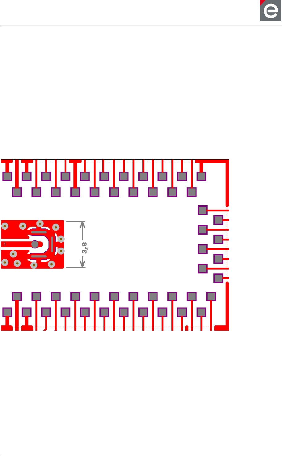
from system ground. The RF ground area in Figure 27 has a vertical dimension of 3.8 mm.
The ground vias are not plugged. In this area are no other radio module signals. An
unintentional short-circuit is therefore accepted. Do not place copper on any other area
among the entire module. Solder stop could be used everywhere.
The RF trace design depends on the used base board and is described detailed in Section
8.5.
Figure 27: Exemplary base board footprint for 22M10 (top view)
User Manual
Version 1.1c
2013-07-01
OEM radio modules deRFmega
www.dresden-elektronik.de
Page 37 of 52
8.2.3. Footprint of deRFmega128-22M12
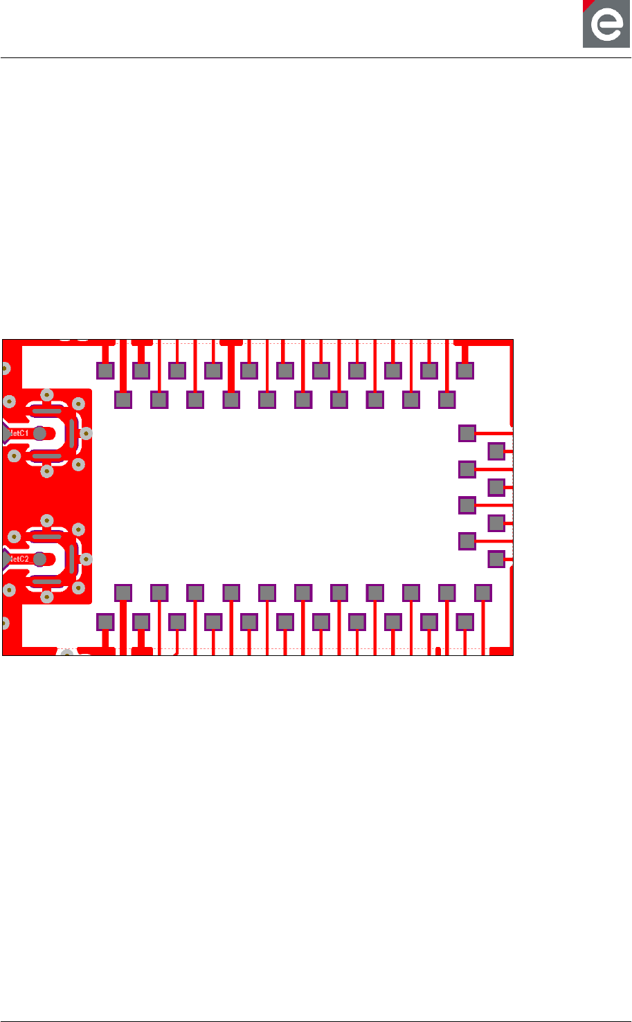
Figure 28 shows an exemplary base board footprint for deRFmega128-22M12. Only the top
layer (red) is visible. The mid and bottom layers are hidden. The pad copper area (red, not
visible) and the paste dimension (grey) have the same size of 0.6 x 0.6 mm. The solder stop
clearance (purple) has a value of 0.1 mm.
The RF ground pads are connected to each other and to the board ground to ensure a
proper ground area. For the most applications it is not necessary to separate the RF ground
from system ground. The RF ground area in Figure 28 has a vertical dimension of 9.4 mm.
The ground vias are not plugged. In this area are no other radio module signals. An
unintentional short-circuit is therefore accepted. Do not place copper on any other area
among the entire module. Solder stop could be used everywhere.
The RF trace design depends on the used base board and is described detailed Section 8.5.
Figure 28: Exemplary base board footprint for 22M12 (top view)
8.3. Ground plane
The performance of RF applications mainly depends on the ground plane design. The often
used chip ceramic antennas are very tiny, but they need a proper ground plane to establish a
good radiation pattern. Every board design is different and cannot easily be compared to
each other. Some practical notes for the ground plane design are described below:
Regard to the design guideline of the antenna manufacturer
Use closed ground planes on the PCB edges on top and bottom layer
Connect the ground planes with lots of vias. Place it inside the PCB like a chessboard
and on the edges very closely.
User Manual
Version 1.1c
2013-07-01
OEM radio modules deRFmega
www.dresden-elektronik.de
Page 38 of 52
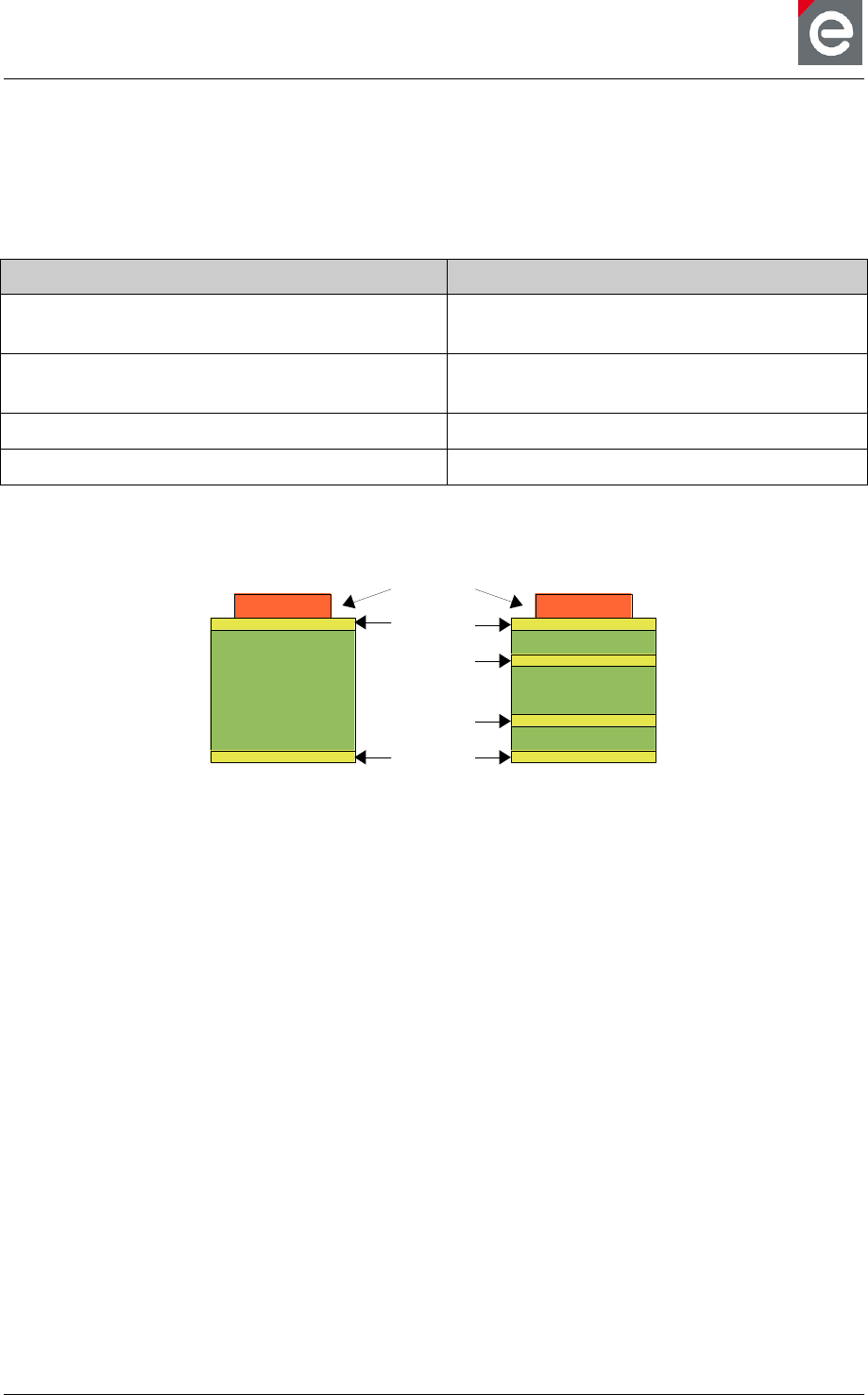
8.4. Layers
The use of 2 or 4 layer boards have advantages and disadvantages for the design of a
custom base board.
Table 8-1: 2 and 4 layer board properties in comparison
2 Layer board
4 Layer board
(-) only 2 layers available for routing the traces
and design a proper ground area
(+) 4 layers available for routing the traces
and design a proper ground area
(-) only 1 layer available for routing the traces
under the module
(+) 3 layers available for routing the traces
under the module
(-) no separate VCC plane usable
(+) separate VCC plane usable
(+) cheaper than 4 layers
(-) more expensive than 2 layers
Top
Bottom
Mid 1
Mid 2
2 Layer 4 Layer
Module
4 Layer Traces under
module:
Not allowed
allowed
allowed
allowed
Traces under
module:
Not allowed
allowed
Figure 29: Layer design of 2 and 4 layer boards
User Manual
Version 1.1c
2013-07-01
OEM radio modules deRFmega
www.dresden-elektronik.de
Page 39 of 52
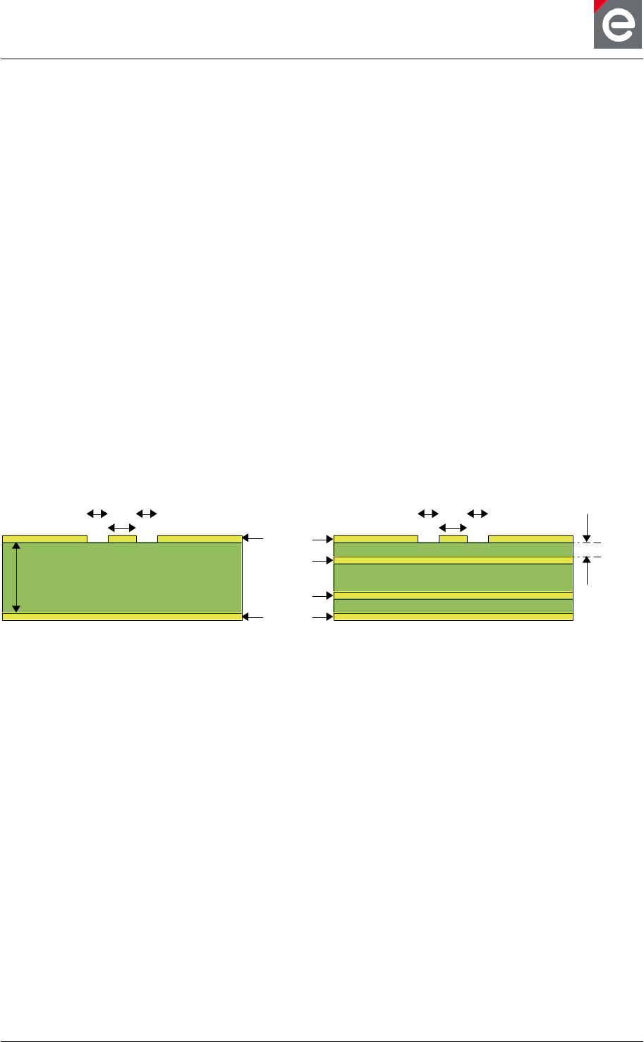
8.5. Traces
Common signal traces should be designed with these guidelines:
Traces on top layer are not allowed under the module (see Figure 29)
Traces on mid layers and bottom layers are allowed (see Figure 29)
Route traces straight away from module (see Figure 26)
Do not use heat traps of components directly on the RF trace
Do not use 90 degree corners. Better is 45 degree or rounded corners.
The trace design for RF signals has a lot of more important points to regard. It defines the
trace impedance and therefore the signal reflection and transmission. The most commonly
used RF trace designs are Microstrip and Grounded Coplanar Wave Guide (GCPW). The
dimension of the trace is depending on the used PCB material, the height of the material to
the next ground plane, a PCB with or without a ground plane, the trace width and for GCPW
the gap to the top ground plane. The calculation is not trivial, therefore specific literature and
web content is available (see [2])
The reference plane to the GCPW should always be a ground area, that means the bottom
layer for a 2 layer design and mid layer 1 for a 4 layer design (see Figure 30). Furthermore,
it is important to use a PCB material with a known layer stack and relative permittivity. Small
differences in the material thickness have a great influence on the trace impedance,
especially on 4 layer designs.
Top
Bottom
Mid 1
Mid 2
2 Layer 4 Layer
h
g g
w
g g
w
h
FR4 ≈ 4.3 FR4 ≈ 4.3
Figure 30: GCPW trace design
User Manual
Version 1.1c
2013-07-01
OEM radio modules deRFmega
www.dresden-elektronik.de
Page 40 of 52
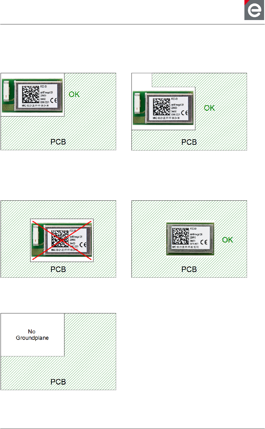
8.6. Placement on the PCB
The PCB design of the radio module base board and placement affects the radio
characteristic. The radio module with chip antenna should be placed at the edge or side of a
base board. The chip antenna should be directed to PCB side.
Figure 31: Placing at the edge
Figure 32: Placing at the center edge
Do not place the chip antenna radio module within the base board. This will effect a very
poor radio performance. Instead radio modules with RF pads could be placed everywhere on
the PCB. But it should be enough space for routing a RF trace to a coaxial connector or to an
onboard antenna.
Figure 33: Placing in the center with antenna
Figure 34: Placing in the center with RF pad
Do not place ground areas below the radio module (see Section 8.4) and near the chip
antenna.
Figure 35: No ground plane under the module

User Manual
Version 1.1c
2013-07-01
OEM radio modules deRFmega
www.dresden-elektronik.de
Page 41 of 52
9. Clock
The radio module contains an onboard 32.768 kHz 20 ppm quartz crystal for the MCU and a
16.000 MHz 10 ppm quartz crystal for the internal transceiver. For optimum RF timing
characteristics it is necessary to use a low tolerance crystal. The watch crystal clocks a timer,
not the processor. The timer is intended to wake-up the processor periodically.
User Manual
Version 1.1c
2013-07-01
OEM radio modules deRFmega
www.dresden-elektronik.de
Page 42 of 52
10. Application circuits
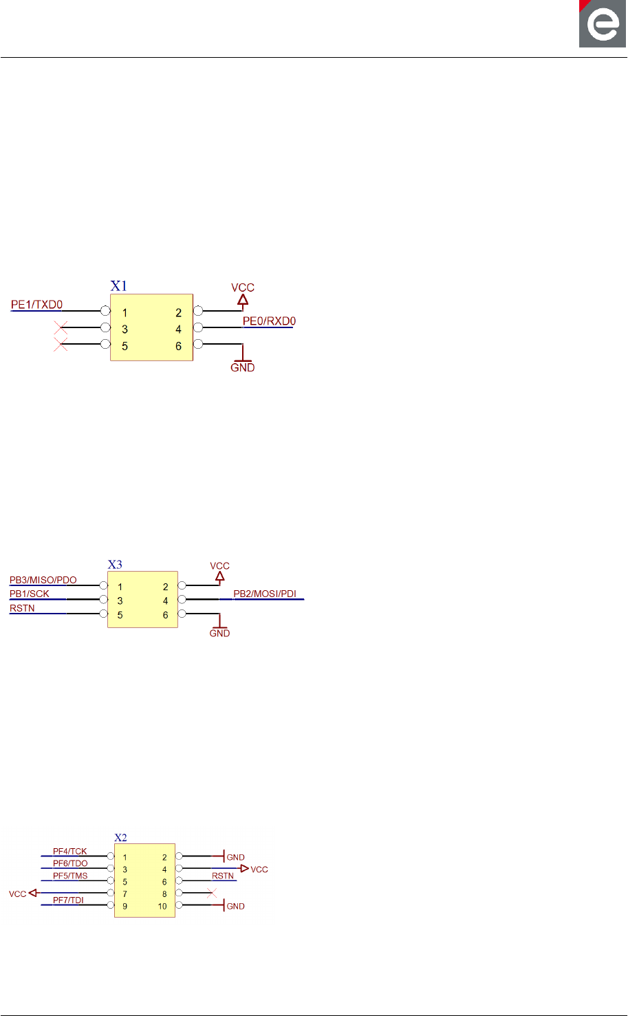
10.1. UART
Two U(S)ART interfaces are available on the radio modules. For communication to a host
with a different supply voltage domain it is necessary to use a level-shifter. We recommend
the USB level shifter by dresden elektronik. The level-shifter can be connected to the custom
base board via 100 mil 2 x 3 pin header. The pin assignment should be designed as below in
Figure 36. For an UART connection it is sufficient to use only TXD, RXD and GROUND
signals.
1. PE1/TXD0
2. VCC
3. Not connected
4. PE0/RXD0
5. Not connected
6. GND
Figure 36: 100 mil 2 x 3 pin header for UART0
10.2. ISP
The AVR based radio modules can be programmed via JTAG and ISP interface. For ISP
connections a 100 mil 2 x 3 pin header should be used. The pin assignment is given in
Figure 37. The MCU ATmega128RFA1 uses the ISP signals PDO and PDI on the same pins
like the SPI with MISO and MOSI. We recommend the use of an ‘AVR ISP programmer’.
1. PB3/MISO/PDO
2. VCC
3. PB1/SCK
4. PB2/MOSI/PDI
5. RSTN
6. GND
Figure 37: 100 mil 2x3 pin header for ISP
10.3. JTAG
The AVR based radio modules can be programmed via JTAG and ISP interface. For JTAG
connections a 100 mil 2 x 5 pin header should be used. The pin assignment is given in
Figure 38. We recommend the use of ‘Atmel AVR Dragon’ or ‘Atmel JTAG ICE mkII’
programmer.
1. PF4/TCK
2. GND
3. PF6/TDO
4. VCC
5. PF5/TMS
6. RSTN
7. VCC
8. Not connected
9. PF7/TDI
10. GND
Figure 38: 100 mil 2x5 pin header for JTAG
User Manual
Version 1.1c
2013-07-01
OEM radio modules deRFmega
www.dresden-elektronik.de
Page 43 of 52
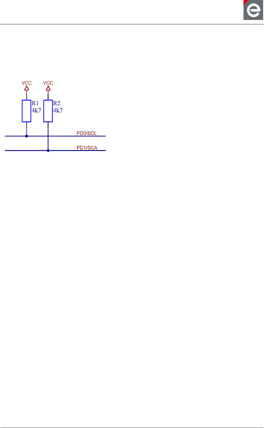
10.4. TWI
The connection of external peripherals or sensors via Two-Wire-Interface is possible by
using the TWI clock signal PD0/SCL and TWI data signal PD1/SCA. The necessary pull-up
resistors must be placed externally on the base board. We recommend the use of 4.7 kΩ
resistors as shown in Figure 39.
Figure 39: Two-Wire-Interface
User Manual
Version 1.1c
2013-07-01
OEM radio modules deRFmega
www.dresden-elektronik.de
Page 44 of 52
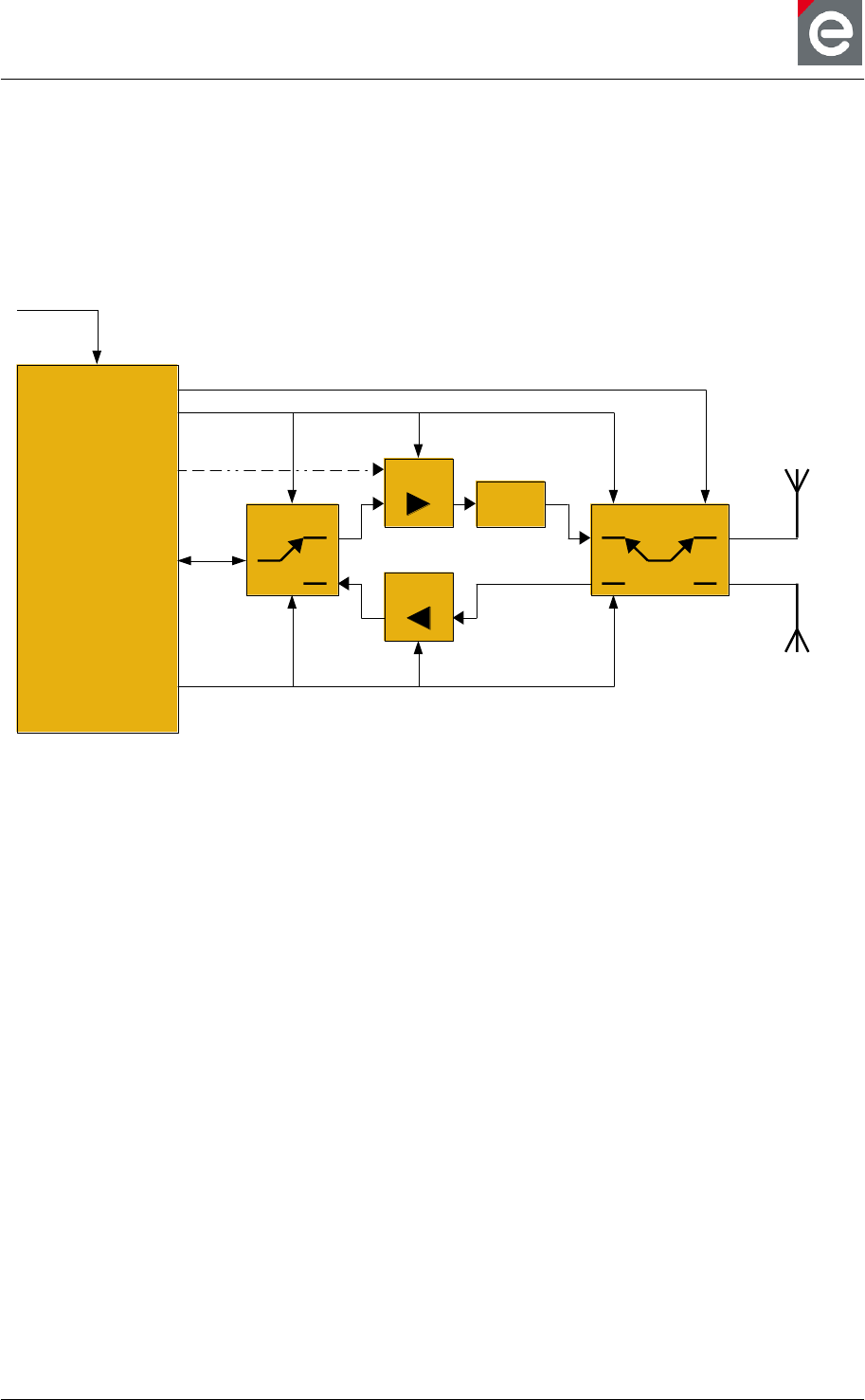
10.5. External front-end and antenna diversity
The radio module deRFmega128-22M10 can be connected with an external front-end
including power amplifier (PA) for transmission and low noise block (LNA) for receiving.
Figure 40 shows a possible design as block diagram. A custom design can contain a single
PA or single LNA or a complete integrated front-end chip. It depends mainly on the
application. Furthermore, it is possible to include a RF switch for driving the antenna diversity
feature.
deRFmega128
22M10
VCC
1.8V to 3.6V
GPIO
for PA on/off PA
LNA
RF switch RF switch
BPF
RFout
ANT0
ANT1
DIG3
DIG4
DIG1
Figure 40: block diagram for external PA/LNA and antenna diversity control
Unbalanced RF output
The radio module 22M10 has a 50 Ω unbalanced RF output. For designs with external RF
power amplifier a RF switch is required to separate the TX and RX path.
RF switches to PA, LNA and antenna
The switch must have 50 Ω inputs and outputs for the RF signal. The switch control could be
realized with the DIG3 and DIG4 signal of the radio module. Refer to Section 7.2.1 for
detailed information.
PA
The PA has to be placed on the TX path after the RF switch. It is important to regard the
PA’s manufacturer datasheet and application notes, especially for designing the power
supply and ground areas. A poor design could cause a very poor RF performance. For
energy efficiency it is useful to activate the PA only during TX signal transmission. In this
case the DIG3 signal can be used as switch for (de-)activating the PA. Some PAs have the
possibility to set them into sleep state. This application can be realized via a dedicated GPIO
pin. Refer to Section 7.2.1 for more information.
BPF
The use of a band-pass filter is optional. It depends on the PA properties. Some PAs have an
internal BPF and other do not have. The BPF is necessary to suppress spurious emissions of
the harmonics and to be compliant with national EMI limits. It is possible to use an integrated
BPF part or discrete parts. The advantage of the first variant is that the BPF characteristic is
known and published in the manufacturer’s datasheet.

User Manual
Version 1.1c
2013-07-01
OEM radio modules deRFmega
www.dresden-elektronik.de
Page 45 of 52
LNA
The LNA could be used to amplify the received signal. Please regard the manufacturer’s
datasheet for a proper design. The control could be done by DIG4 signal. Refer to
Section 7.2.1 for more information.
RF switch for antenna diversity
The switch must have 50 Ω inputs and outputs for the RF signal. It is possible to use a
separate switch with 2 inputs and 2 outputs or use another (third) switch following the switch
required for the PA/LNA. Antenna diversity switching could be controlled via DIG1. Refer to
Section 7.2.1 for more information.
Certification
The customer has to ensure, that custom front-end and antenna diversity designs based on
the radio module deRFmega128-22M10 will meet all national regulatory requirements of the
assignment location and to have all necessary certifications, device registration or
identification numbers.
For long range applications we recommend the use of the deRF-mega128-22M12 radio
module which already includes PA, LNA, BPF, RF switches and antenna diversity. This
module will be provided by dresden elektronik with certified reference designs for EU and US
applications that meet all regulatory requirements and reduce custom design costs.
User Manual
Version 1.1c
2013-07-01
OEM radio modules deRFmega
www.dresden-elektronik.de
Page 46 of 52
11. Programming
The programming procedures are described in the user manual [3], which is online available
on dresden elektronik webpage. It describes the update process of the radio module, the
required software and hardware for programming via JTAG and the driver installation on
different operating systems.
12. Pre-flashed firmware
Actually, the radio modules will be delivered without pre-flashed firmware.
13. Adapter boards
dresden elektronik offers these radio modules soldered on suitable adapter boards
(deRFholder). These boards can be plugged into dresden elektronik's development hardware
platforms deRFbreakout Board, deRFnode or deRFgateway. For detailed information please
refer to the deRFholder datasheets [4] and [5].
Figure 41: deRFmega128-22T00 with radio module deRFmega128-22M00
Figure 42: deRFmega128-22T02 with radio module deRFmega128-22M10
Figure 43: deRFmega128-22T13 with radio module deRFmega128-22M12

User Manual
Version 1.1c
2013-07-01
OEM radio modules deRFmega
www.dresden-elektronik.de
Page 47 of 52
14. Radio certification
14.1. United States (FCC)
The deRFmega128-22M00, deRFmega128-22M10 and deRFmega128-22M12 comply with
the requirements of FCC part 15. The certification process for deRFmega128-22M10 and
deRFmega128-22M12 is pending.
To fulfill FCC Certification requirements, an OEM manufacturer must comply with the
following regulations:
The modular transmitter must be labeled with its own FCC ID number, and, if the FCC ID is
not visible when the module is installed inside another device, then the outside of the device
into which the module is installed must also display a label referring to the enclosed module.
This exterior label can use wording such as the following. Any similar wording that expresses
the same meaning may be used.
Sample label for radio module deRFmega128-22M00:
FCC-ID: XVV-MEGA22M00
This device complies with Part 15 of the FCC Rules. Operation is subject to the following two
conditions: (1) this device may not cause harmful interference, and (2) this device must
accept any interference received, including interference that may cause undesired operation.
The Original Equipment Manufacturer (OEM) must ensure that the OEM modular transmitter
must be labeled with its own FCC ID number. This includes a clearly visible label on the
outside of the final product enclosure that displays the contents shown below. If the FCC ID
is not visible when the equipment is installed inside another device, then the outside of the
device into which the equipment is installed must also display a label referring to the
enclosed equipment.
This equipment complies with Part 15 of the FCC Rules. Operation is subject to the following
two conditions: (1) this device may not cause harmful interference, and (2) this device must
accept any interference received, including interference that may cause undesired operation
(FCC 15.19). The internal / external antenna(s) used for this mobile transmitter must provide
a separation distance of at least 20 cm from all persons and must not be co-located or
operating in conjunction with any other antenna or transmitter.
Installers must be provided with antenna installation instructions and transmitter operating
conditions for satisfying RF exposure compliance. This device is approved as a mobile
device with respect to RF exposure compliance, and may only be marketed to OEM
installers. Use in portable exposure conditions (FCC 2.1093) requires separate equipment
authorization.
Modifications not expressly approved by this company could void the user's authority to
operate this equipment (FCC section 15.21).
This equipment has been tested and found to comply with the limits for a Class A digital
device, pursuant to Part 15 of the FCC Rules. These limits are designed to provide
reasonable protection against harmful interference when the equipment is operated in a
commercial environment. This equipment generates, uses, and can radiate radio frequency
energy and, if not installed and used in accordance with the instruction manual, may cause

User Manual
Version 1.1c
2013-07-01
OEM radio modules deRFmega
www.dresden-elektronik.de
Page 48 of 52
harmful interference to radio communications. Operation of this equipment in a residential
area is likely to cause harmful interference in which case the user will be required to correct
the interference at his own expense (FCC section 15.105).
14.2. European Union (ETSI)
The deRFmega128-22M00, deRFmega128-22M10 and deRFmega128-22M12 are conform
for use in European Union countries.
If the deRFmega128-22M00, deRFmega128-22M10 and deRFmega128-22M12 modules are
incorporated into a product, the manufacturer must ensure compliance of the final product to
the European harmonized EMC and low-voltage/safety standards. A Declaration of
Conformity must be issued for each of these standards and kept on file as described in
Annex II of the R&TTE Directive.
The manufacturer must maintain a copy of the deRFmega128-22M00, deRFmega128-
22M10 and deRFmega128-22M12 modules documentation and ensure the final product
does not exceed the specified power ratings, antenna specifications, and/or installation
requirements as specified in the user manual. If any of these specifications are exceeded in
the final product, a submission must be made to a notified body for compliance testing to all
required standards.
The CE marking must be affixed to a visible location on the OEM product. The CE mark shall
consist of the initials "CE" taking the following form:
If the CE marking is reduced or enlarged, the proportions must be respected.
The CE marking must have a height of at least 5 mm except where this is not
possible on account of the nature of the apparatus.
The CE marking must be affixed visibly, legibly, and indelibly.
More detailed information about CE marking requirements can be found in [6].
14.3. Approved antennas
The deRFmega128-22M00 has an integrated chip antenna. The design is fully compliant with
all regulations.
The deRFmega128-22M10 and deRFmega128-22M12 will be tested with external antennas.
The approved antenna list will be updated after certification process has finished.
User Manual
Version 1.1c
2013-07-01
OEM radio modules deRFmega
www.dresden-elektronik.de
Page 49 of 52
15. Ordering information
The product name includes the following information:
deRF xxxx - x x x xx
Features
Form Factor
Flash Memory
Frequency Range
Product / Chipset
Table 15-1: Product name code
Product name code
Information
Code
Explanation
Comments
Product / Chipset
mega128
ATmega128RFA1
MCU
Frequency Range
2
2.4 GHz
Flash memory
2
128 kByte
Size
M
Mini module
solderable
Features
00
chip antenna
onboard
10
RFOUT pad
12
Internal front-end,
Antenna diversity,
2x RFOUT pads
Table 15-2: Ordering information
Ordering information
Part number
Product name
Comments
BN-034491
deRFmega128-22M00 NO FW
solderable radio module with onboard chip
antenna, no pre-flashed firmware
BN-034492
deRFmega128-22M10 NO FW
solderable radio module with RFOUT pad,
no pre-flashed firmware
BN-034368
deRFmega128-22M12 NO FW
solderable radio module with onboard
front-end, antenna diversity RFOUT pads,
no pre-flashed firmware

User Manual
Version 1.1c
2013-07-01
OEM radio modules deRFmega
www.dresden-elektronik.de
Page 50 of 52
16. Packaging dimension
The radio modules will be delivered in Tape & Reel packing.
Further information will be described in this section soon.
17. Revision notes
Actually, no design issues of the radio modules are known.
All errata of the AVR MCU ATmega128RFA1 are described in the datasheet [1].

User Manual
Version 1.1c
2013-07-01
OEM radio modules deRFmega
www.dresden-elektronik.de
Page 51 of 52
18. References
[1] ATmega128RFA1: 8-bit AVR Microcontroller with Low Power 2.4 GHz Transceiver
for ZigBee and IEEE802.15.4; Datasheet, URL: http://www.atmel.com
[2] AppCAD Version 3.0.2, RF & Microwave design software, Agilent Technologies;
URL: http://www.hp.woodshot.com
[3] User Manual deRFusb Firmware Update, URL: http://www.dresden-elektronik.de/
funktechnik/uploads/media/deRFusb_Firmware_Update-BHB-en.pdf
[4] Datasheet deRFholder 22T00 | 22T02, URL: http://www.dresden-elektronik.de/
funktechnik/uploads/media/deRFholder-22T00_22T02-DBT-en.pdf
[5] Datasheet deRFholder 22T13, URL: http://www.dresden-elektronik.de/
funktechnik/uploads/media/deRFholder-22T13-DBT-en.pdf
[6] Directive 1999/5/EC, European Parliament and the Council, 9 March 1999, section 12

User Manual
Version 1.1c
2013-07-01
OEM radio modules deRFmega
www.dresden-elektronik.de
Page 52 of 52
dresden elektronik ingenieurtechnik gmbh
Enno-Heidebroek-Straße 12
01237 Dresden
GERMANY
Phone +49 351 - 31850 0
Fax +49 351 - 31850 10
Email wireless@dresden-elektronik.de
Trademarks and acknowledgements
IEEE 802.15.4™ is a trademark of the Institute of Electrical and Electronics Engineers (IEEE).
ZigBee® is a registered trademark of the ZigBee Alliance.
All trademarks are registered by their respective owners in certain countries only. Other brands and
their products are trademarks or registered trademarks of their respective holders and should be noted
as such.
Disclaimer
This note is provided as-is and is subject to change without notice. Except to the extent prohibited by
law, dresden elektronik ingenieurtechnik gmbh makes no express or implied warranty of any kind with
regard to this guide, and specifically disclaims the implied warranties and conditions of merchantability
and fitness for a particular purpose. dresden elektronik ingenieurtechnik gmbh shall not be liable for
any errors or incidental or consequential damage in connection with the furnishing, performance or
use of this guide.
No part of this publication may be reproduced, stored in a retrieval system, or transmitted in any form
or any means electronic or mechanical, including photocopying and recording, for any purpose other
than the purchaser’s personal use, without the written permission of dresden elektronik
ingenieurtechnik gmbh.
Copyright © 2013 dresden elektronik ingenieurtechnik gmbh. All rights reserved.